1
SINGLE
BOARD
4U
SYSTEMS
Little Board lPC
lM
Technical Manual
PIN: A74081
Revision:
A
Ampro Computers, Incorporated
990 Almanor Avenue. Sunnyvale, CA 94086
Tel (408) 522-2100 • FAX (408) 720-1305
.
NOTICE
DISCLAIMER
Ampro Computers, Incorporated makes no representations or wan'anties with respect to the
contents 01 this manual and specifically disclaims any implkd warranties 01 merchantability or
fitness lor any particuJar purpose. Ampro shall under no circumstances ·be liable lor incidental
or consequential damages or related expenses resulting from the use 01 this product, even il it has
been notifkdol the possibility 01 such damages. Ampro reserves the right to revise this publication from time to time without obligation to notify any person 01 such revisions. II e"ors are
lound, please contact Ampro at the address listed on the tiIJe page 01 this document.
TRADEMARKS
Little Board, StackPlane, MiniModule, MiniBac/cplane: Ampro Computers, Inc.
dBASE: Ashton-Tate
Hercules: Hercules Computer Technology
IBM, XT, AT: International Business Machines Corporation
LOTUS 1-2-3: Lotus Development Corp.
MS-Dos, Flight Simulator: Microsoft Corp.
DR DOS: Digital Research, Inc.
COPYRIGHT 1990 AMPRO COMPUTERS INCORPORATED
No part 01 this document may be reproduced, transmitted, transcribed, stored in a retrieval
system, or translated into any language or computer language, in any lorm or by any means,
electronic, mechanical, magnetic, optica~ chemical, manual, or otherwise, without the prior
written permission 01 Ampro Computers, Incorporated.
iii
PREFACE
... This manual is for ·integrators and..programme.uof ~ystems-based entbe-Ampr.a--bittle
Board/PC single board computer. It contains information on hardware requirements and
interconnection, and details of how to program the system. There are five chapters, organized as follows:
•
Chapter 1 Introduction -- General information pertaining to the Little Board/PC, its
major features, and a brief functional description.
•
Chapter 2 Hardware Configuration - Descriptions of the external components necessaxy to construct systems based on the Little Board/PC with floppy and hard disk drives.
Included are tables listing the pin outs of each of the board's connectors, board jumper
conftgUI'ation, and considerations and specifications concerning peripheral devices.
•
Chapter 3 - Software Configuration An overview of the system features, conftgUI'ation
options, and utilities that are available under the "DOS" (PC-DOS, MS-DOS, or DRDOS) operating system, including system setup guidelines.
•
Chapter 4 1beory of Operation -- Detailed technical information on Little Board/PC
hardware.
•
Chapter 5 Programmers' Reference -- Port addresses and other programming considerations for custom programming of the Little Board/PC, including information pertaining to use of the Ampro SCSI/BIOS.
iv
CONTENTS
CHAPTER 1 -INTRODUCTION
1.1 General Description .......................................................................................................1-1
1.2 Little BoardlPC Feaqu-es ..............................................................................................1-2
1.3 Little BoardlPC S~cifications ..................................................................................... 1-2
CHAPTER 2 - HARDWARE CONFIGURATION
2.1 Introduction .....................................................................................................................2-1
2.1.1
Interface Connectors......................................................................................2-1
2.1.2
Jumper Options ..............................................................................................2-3
2.2 DC Power Input - Jl .......................................................................................................2-4
2.3 Onboard Options ............................................................................................................2-5
2.3.1
DRAM Memory .............................................................................................2-5
2.3.2
Math Coprocessor (JI0) ................................................................................2-6
2.3.3
Byte-Wide Memory Sockets..........................................................................2-7
2.3.4
Battery-Backed Clock Module......................................................................2-9
2.3.5
Video Display Mode Jumpering...................................................................2-9
2.3.6
I/O Wait State Option ...................................................................................2-10
2.4 Peripheral Interface ConfJgUration and Connections ................................................2-10
2.4.1
Utility Connector - J4.....................................................................................2-10
2.4.2
Keyboard - J5 ..................................................................................................2-12
2.4.3
Parallel Printer Port - J6................................................................................2-12
2.4.4
PC Compatible Serial Port - J3 ....................................................................2-14
2.4.5
V40 Serial Port - J2 ........................................................................................2-15
2.4.6
Floppy Disk Interface - J8 .............................................................................2-16
2.5 SCSI Interface - 17 ..........................................................................................................2-21
2.5.1
Normal Use of SCSI.......................................................................................2-22
2.5.2
The Ampro SCSI/BIOS ................................................................................2-22
2.5.3
Simple Bidirectional 1/0 ...............................................................................2-23
2.5.4
SCSI Interface ConfJgUration. .......................................................................2-23
2.6 PC Expansion Bus - J9 ...................................................................................................2-26
2.6.1
Onboard MiniModule Header and Bus Expansion ...................................2-26
2.6.2
Using Standard PC and AT Bus Cards .......................................................2-27
2.6.3
Expansion Bus Cable Considerations .....................................;....................2-27
2.6.4
Expansion Bus Connector Pinouts ...............................................................2-28
CHAPTER 3 - SOFTWARE CONFIGURATION
3.1 Introduction ............................................................................;........................................3-1
3.1.1
Conventions .....................................................................................................3-1
3.2 Operation with DOS .......................................................................................................3-2
3.2.1
ConfJgUration Options ...................................................................................3-3
3.2.2
Little Board/PC Utilities Overview .............................................................3-3
3.3 Wait State (CPU Speed) Initialization.........................................................................3-4
3.4 Using a Parallel Printer ..................................................................................................3-4
3.5 Using the PC Compauble Serial Port ..........................................................................3-5
3.5.1
Serial Port Initialization.................................................................................3-5
3.5.2
Using a Serial Printer.....................................................................................3-6
3.5.3
Using a Serial Modem ...................................................................................3-6
3.6 Using the Non-standard V40 Serial Port .....................................................................3-7
3.6.1
Serial Console Option ....................................................................................3-7
3.6.2
Serial Printer Option......................................................................................3-7
v
3.7
3.8
Using Floppy Drl\ies .......................................................................................................3-8
Using SCSI Hard Disk Drl\ies .......................................................................................3-8
3.8~1
Hardware Preparation ...................................................................................3-8
3.8.2
Preparation for DOS Use ..............................................................................3-9
CHAPTER .. - THEORY OF OPERATION
4.1 Introduction .....................................................................................................................4-1
4.2 Technical References .....................................................................................................4-1
4.3 CPU and General Architecture ....................................................................................2-4
4.4 V40 Internal Peripherals ................................................................................................4-4
4.4.1
Interrupt Controller .......................................................................................4-5
4.4.2
COuntertrimers..............................................................................................4-5
DMA Controller .............................................................................................4-6
4.4.3
4.4.4
Wait State Control..........................................................................................4-7
4.5 Onboard Memory ...........................................................................................................4-8
4.5.1
DRAM Sockets ...............................................................................................4-8
4.5.2
EPROM Socket ..............................................................................................4-9
4.5.3
Byte·Wide Sockets (U15 and U26) ..............................................................4-9
4.6 Onboard I/O Interfaces ...............................................................................-..................4-10
4.6.1
V40 Serial Port................................................................................................4-10
4.6.2
Parallel Printer Port .......................................................................................4-11
Keyboard Interfaces .......................................................................................4-11
4.6.3
4.6.4
Speaker Interface............................................................................................4-12
4.6.5
PC COnfJgUration Switches............................................................................4-12
PC Serial Port .................................................................................................4-12
4.6.6
4.6.7
Floppy Disk Controller ..................................................................................4-13
SCSI Bus Interface ...........................................:.............................................4-13
4.6.8
4.7 PC Bus Interface .............................................................................................................4-14
CHAPTER 5 - PROGRAMMING INFORMATION
5.1 Introduction .....................................................................................................................5-1
5.2 System Memory Map......................................................................................................5-1
5.3 I/O Address Map............................................................................................................5-1
5.4 V40 Internal Registers....................................................................................................5-4
5.5 V40 Initialization ............................................................................................................ .5-4
5.6 SCSI Interface .................................................................................................................5-7
5.6.1
SCSI Programming.........................................................................................5-7
5.6.2
Simple Bidirectional I/O ...............................................................................5-8
5.6.3
Jumper Input Port ..........................................................................................5-8
5.6.4
Ampro SCSI/BIOS ........................................................................................5-9
APPENDIX A - UTTLE BOARD/PC UTiUTIES SOFTWARE
CONDRVR.syS
PRNDRVR.syS
SCSI·ID
SCSICOMP
SCSICOPY
SCSIFMT
SCSIPARK
SCSITOOL
SETWAIT
FIGURES
Figure 1-1
Figure 2-1
Figure 2-2
Figure 4-1
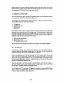
Little Board/PC Mechanical Dimensions ................................................... 1-4
Connector and Jumper Locations ................................................................2-2
Power Connector Wiring ...............................................................................2-4
Little Board/PC Block Diagram ..................................................................4-1
TABLES
Table 2-1
Table 2-2
Table 2-3
Table 2-4
Table 2-5
Table 2-6
Table 2-7
Table 2-8
Table 2-9
Table 2-10
Table 2-11
Table 2-U
Table 2-13
Table 2-14
Table 2-15
Table 2-16
Table 2-17
Table 2-18
Table 2-19
Table 2-20
Table 2-21
Table 2-22
Table 2-23
Table 2-24
Table 2-25A
Table 2-25B
Summary of Connector Usage ...................................................................... 2-3
Power Connector Usage (J1) ........................................................................2-4
Power Consumption vs. Configuration ........................................................ 2-5
Onboard DRAM Memory Size Jumpering.................................................2-6
U26 Device Jumpering ..................................................................................2-8
U15 Device Jumpering ..................................................................................2-9
Video Display Mode ...................................................................................... 2-9
I/O Wait States...............................................................................................2-10
Utility Connector (J4) ....................................................................................2-11
Keyboard Connector (J5) ..............................................................................2-U
Parallel Printer Connector (J6) ....................................................................2-13
Parallel Printer Configuration ......................................................................2-13
PC Serial Port Connections...........................................................................2-14
PC Serial Port Configurations ......................................................................2-15
V40 Serial Port Connections .........................................................................2-16
Supported Floppy Formats ............................................................................ 2-17
Floppy Disk Interface Connector (J8) .........................................................2-18
Floppy Drive Quantity ...................................................................................2-19
Drive A Type Selection..................................................................................2-19
Drive B Type Selection ..................................................................................2-19
Floppy Interface Options ...............................................................................2-20
SCSI Interface Connector (J7) .....................................................................2-21
SCSI Initiator ID Jumpering .........................................................................2-24
SCSI Interface Option Jumpers ....................................................................2-25
PC Expansion Bus Connector, AI-A32 (J9) ............................................... 2-29
PC Expansion Bus Connector, B1-B32 (J9) ...............................................2-30
Table 4-1
DMA Channel Remapping ...........................................................................4-7
Table 5-1
Table 5-2
Table 5-3
Table 5-4
Table 5-5
Table 5-6
Little Board/PC Memory Map.....................................................................5-2
Little Board/PC I/O Map.............................................................................5-3
V40 Internal Peripheral Control Registers .................................................5-5
ROM-BIOS Default V40 Initialization .......................................................5-6
53C8O Internal Registers ...............................................................................5-7
Jumper Input Port ..........................................................................................5-9
CHAPTER 1
INTRODUCTION
1.1 GENERAL DESCRIPTION
The Little Board/PC provides system designers with a highly compact, self-contained,low
power, PC-compatible single board system that requires no more space than a half height 51/4" disk drive. This unique single board system is functionally equivalent to a PC/XT
motherboard and three or four expansion cards.
The Little Board/PC is ideally suited for embedded microcomputer applications where PC
software and bus compatibility are required, and where low power consumption (4 watts),
small size (5.75" x 8" x 1.1", wide temperature range (0-700 C), and high reliability are critical.
In addition, its ability to use rugged media like EPROM and nonvolatile RAM instead of disk
drives makes the Little Board/PC especially well suited for use in rugged or harsh operating
environments.
Typical applications for the Little Board/PC include:
•
•
•
•
•
•
•
Data acquisition
Portable instruments
Protocol conversion
Telecommunications
Security systems
Vending machines
Robot and machine control
•
•
•
•
•
•
Diskless workstations
Remote data logging
Point-of-sale terminals
Network servers
Distributed processing
Medical instruments
The Little Board/PC includes a CMOS NEC V40 enhanced 8088-compatible microprocessor,
up to 768Kbytes of on-board RAM, and a full complement of PC compatible controllers.
Peripheral controllers are included for serial, printer, keyboard, speaker, and floppy interfacing. In addition, two industry standard system expansion buses -- a PC Expansion Bus and a
Small Computer System Interface (SCSI) -- offer system expansion flexibility.
An expansion connector is provided onboard for Ampro MiniModule expansion boards which
attach directly to the Little Board/PC. When installed, a MiniModule fits entirely within the
Little Board/PC's outline dimensions.
Standard PC bus plug-in cards can be connected to the Little Board/PC using a ribbon cable
from the PC bus expansion connector. The innovative Ampro StackPlane™ expansion option
permits a PC bus card to be mounted parallel to the Little Board/PC without additional
hardware. Also available is a compact 2-s10t passive backplane, which accommodates two PC
bus cards.
Support for SCSI direct access devices as boot or data devices is included directly in the
board's ROM-BIOS. This SCSI/BIOS feature allows a wide variety of hard disks, floppy
drives, bubble memory drives, tape drives, and other SCSI devices to be used interchangeably,
greatly enhancing the ease and flexibility of system integration, maintenance, and upgrades.
Sockets on the Little Board/PC allow onboard EPROM (up to 256K bytes) or battery backed
RAM (up to64K bytes) to function as a bootable PC-DOS compatible "Solid State Disk"
(SSD) drive. SSD operation offers several key advantages, including improved speed, reliability, and ruggedness, and reduced power consumption. Ampro's optional SSD support soft-
1-1
ware converts DOS based applications into EPROM format automatically, without the need
for special programming techniques. In addition, Ampro's SSD Expansion board, which
matches the 5.75" x 8" form factor of the Little Board/PC, can be used to add sixteen additional byte-wide devices (EPROM or battery-backed RAM) for larger SSDs.
A key advantage of the PC compatibility of the Little Board/PC is that it runs the thousands
of software applications and utility packages developed for the IBM PC. Language compilers,
debugging aids, and software support packages for graphics, windowing, multi-tasking, user
interfaces, etc., are readily available. In addition there is a large and growing selection of
DOS programs targeted at industrial and commercial applications such as communications,
data acquisition and control, terminal emulation, protocol conversion, etc.
The Little BoardlPC is a member of Ampro's growing family of mM compatible single board
systems. These products offer a broad range of price, performance, and feature alternatives in
a consistent physical and functional format.
1.2 UTTLE BOARD/PC FEATURES
•
•
•
•
•
•
•
•
All the functions of a PC/XT motherboard and 4 expansion cards in the space of a halfheight 5-1/4" disk drive
Up to 768K bytes RAM, 256K bytes EPROM
Two serial ports and a parallel printer port
Mini/Micro floppy controller (360K, 720K, 1.2M, l.44M byte formats)
SCSI controller for hard disks, tape, other SCSI devices, or general purpose digital I/O
Diskless operation using onboard byte-wide sockets for Solid State Disk
Small size, + 5V only operation, and low power consumption; ideal for embedded applications
Expandable with Ampro MiniModules or standard PC bus cards
1.3 UTTLE BOARD/PC SPECIFICATIONS
CPU And Onboard Memory
• NEC V40 CPU (8088 superset), 7.16 MHz
• 256K, S12K, or 768K bytes DRAM with parity
• PC-compatible ROM-BIOS with Ampro extensions
• Two spare 28-pin byte-wide memory sockets at EOOOOh to EFFFFh and FOOOOh to
F7FFFh. Used with:
27256 32K byte EPROMs
27512 64K byte EPROMs
27011128K byte page mode EPROMs
62256 32K byte static RAMs
32K byte nonvolatile RAMs
PC-Compatible Controllers
• Standard DMA/Interrupt/Timer support
7 interrupt channels
-- 3 DMA channels
-- 3 programmable counter/timers
• Two RS232C ports with software controlled baud rates
PC-compatible COM port (8250) with full handshaking
Nonstandard OEM serial port with two active handshake lines
-- Onboard + 1- 9VDC generation
1-2
•
•
•
•
•
Parallel printer port
Standard PC keyboard port
Speaker port with 0.1 watt drive
Optional battery-backed time-of-day clock with 10 year internal lithium battery
PC-compatible mini (5-1/4") and micro (3-1/2") floppy controller
-- 2 drive selects, 1-2 sided, l5O/SOOK bps data rates
-- ROM-BIOS supports all standard formats (320K/720K/1.2M/1.4M)
-- Reliable all-digital phase-locked loop and write precompensation
-- Disk change sense line supported
SCSI Interface
•
•
•
•
Ansi X3.131 (SCSI) compatible
Based on popular 53C80 SCSI bus controller
Usable as 16 (9 bidirectional, 7 input only) general purpose programmed digital I/O
lines (48 rnA sink)
Up to BOOK byte/sec data throughput
Physical
• Size: 8.0" x 5.75" x 1.1" (5-1/4" disk drive form factor)
• Provision for one onboard Ampro MiniModule
• Power requirements: +5V + /- 5% at 800 rnA (typical)
• 4-layer PCB, with full ground and power planes for low noise
• Operating temperature: 0-700 C, 5-95% relative humidity (non-condensing)
• Storage temperature: _55 0 to + 850 C
• Weight: 8.90z. (includes 3 SIMM RAM modules)
1-3
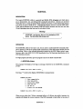
.1~W
2.700
5.750
5.520 -.-.-.--.-..-.--.-.-.-.--.-.-.-.--.-.-.-.--.-.-.-.--.-.-.-
4.900
6.475
-+- --------------------',-----''''--------'----'------------------"----"'---'''''.,,'----- -tooi
I
7.225
iJ7.------------.....-....+-----------..-.......... --.----" 5.420
I
)
,./
///
(
;
!;
J1
1
!
;
.1~5p[A· '_"_"''''
I
-- ..........-..... ..
........
_- ..
-1------1-----1---
I
:,:
........
.~
I
4.015
..--......-........-........-....------·~~l::.::::¢
3.315
..-........-........-........-........-........--1"....-........-........-........-........-........-........-........------'®.
;
,
!
1
J.B
-------~---------------~~if =-.:::~:
I
J5
t]----....- ....-1.900
I
J 6 - ..-.... ----..... 1.500
.900 "'"
.!i=========J,,9========-====_
.800 ......,.: =::==:::::::==:::::::==:::::::::::::::::::::::::: .:::::::::::::::::::::~:.:::::::.::::.:...: .
I
230 ......_--_ .. _. __ ._._._. __ .... _.... __._....... _--_._._. __._._.- ;-- ._.__ ._._-_.__ ._...._. __ ._ .......__._.... _. __ .......... __ .... -_.. _-_ ......_.. _-_...._._. __.-;- -;o- - . f - - - - - - - - - - - - . . J i
i i
i
o
1.800
//' I
5.080
4.920
NOTES: • Shows Pin 1 Location
Values are in inches, +/- .01 in.
Figure 1-1. Mechanical Dimensions
i
5.425
CHAPTER 2
HARDWARE CONFIGURATION
2.1 INTRODUCTION
This chapter describes what is required to integrate the Little Board/PC with a wide variety
of external devices, including keyboards, printers, modems, floppy and hard disk drives, and
monitors. Information is provided regarding the board's connector signals and pinouts,
external device requirements, interconnection cable wiring, and board configuration.
Also covered in this chapter is the configuration and initialization requirements of standard
and optional onboard devices. These include both the standard items such as the DRAM
memory, battery-backed real time clock, and CPU speed control functions, as well as several
optional additions such as EPROM and NOVRAM Solid State Disk drives, and a variety of
onboard expansion modules including the Ampro MiniModule video controllers.
It is important to note, however, that many of the board's functions are software rather than
hardware controlled. Therefore, many of the features and functions '"fescribed in this manual
assume the presence of the board's standard ROM-BIOS for their operation. Refer to
Chapter 3 for typical software configuration information, and to Chapters 4 and S' for technical details regarding the board's hardware and software functions.
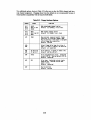
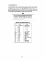
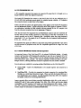
2.1.1 Interface Connectors
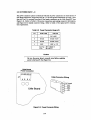
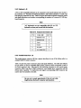
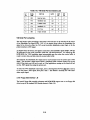
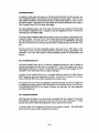
Figure 2-1 shows the board's interface connectors (11-110). Table 2-1 summarizes the board's
connectors interface assignments. Connector pinouts and signal definitions are provided in
the sections of this chapter that cover each connector interface.
All of the board's peripheralI/O interface connectors (J2-J8) are dual row male header
connectors, of varying sizes. Each of these headers can be mated with either flat ribbon
(IDC) or discretely wired connectors. J2, 13, J4, J5, and J6 have been placed together at one
end of the board so that a single 64-position header plug can mate with the entire group.
In some applications it is preferable to plug a specialized PC board assembly onto several or
all of the I/O connectors (J2-J8). This allows you to eliminate cables, meet packaging requirements, add EMI ftltering, or in other ways customize the installation of the Little
Board/PC in your application. In addition, one dual-row male header provides the PC
expansion bus for onboard MiniModule expansion.
2-1
1ST 256K DRAM
2ND 256K DRAM
----------------------1
f-
3RD 256K DRAM
~~
...
V
J7
<-
18~.,. I:~~ ,,0 I~~
O
1
f
~ il··
..
Co>
8s
a0
~
'-----------------------'..
,- 001
l~
W5
.-----v-S----I
W39
W6
i Il7Nr I
IUiI V'~
_
J2~
.....
J3
IUiIW40
J8
~
W48'_ool
I\)
"0
Vlq
I
I\)
-,O ..........
-a. .......... ......
r -________~~~Co>~.~m..... ~
V I
~L_I_ _---'
1 2
J5t]
12
W46~
W21~
lJ
z
--:-==_--'
W36 I-
J6
::~~
"I. . ______
001
U
W10
0
W31
o~
W191Ui1
Figure 2-1. Connector and Jumper locations
~W32
L_______--'
~ W33
W35
,-,-,-,
000
W36
W37
Table 2-1. Summary of Connector Usage
SEGMENT
FUNCTION
SIZE
J1
Power Input
4-pin
J2 (*)
V40 Serial
6-pin
J3 (*)
PC Serial
10-pin
J4
Util ity
10-pin
JS
Keyboard
6-pin
J6
Printer
26-pin
J7
SCSI
50-pin
J8
Floppy
34-pin
J9
PC Bus
64-pin
J10
Math Option
40-pin
(*) J2 and J3 are combi ned on a
single 16-pin connector.
2.1.2 Jumper Options
For normal PC compatible operation, no special jumpering of the Little Board/PC is required. As shipped from the factory, the board can be connected to appropriate peripherals
and operated immediately. Typically, the only jumpers you need be concerned with are the
following:
•
Floppy drive quantity. See Table 2-16; default = 2 drives.
•
Floppy drive type. See Table 2-17 and 2-18; default = 360K drives.
•
Video mode. See Table 2-21; default = color.
•
SCSI bus disable. See Section 2.5; default = enabled.
Note
If you do not use SCSI, be sure to use the disable jumper
as discussed in Section 2.5, as it eliminates system boot
delay.
Each of the board's jumper options is referred to by a "W' number (i.e. W1-W47). In nearly
every case, the jumper option consists of a pair of pins which is either shorted or unshorted by
installing or removing a shorting block. Several jumper options consist of three pins. For
these jumper options, there are three choices: shorting pin 1 to pin 2; shorting pin 2 to pin 3;
or shorting neither. One exception is W45, which has 6 pins -- labeled on the board.
The pin numbering convention for all jumper options (except W45) is as follows: assuming
the orientation of the Little Board/PC shown in Figure 2-1, pin 1 is either the one on the left
or the one on the top, depending on which axis the jumper group occupies.
2-3
2.2 DC POWER INPUT - J1
The power connector pinout is identical with that of power connectors on nearly allS-1/4
inch floppy disk drives, except that only the + 5 volt and ground connections are used. Note
that pin 1 on 11 is reversed from that of the header connectors on the Little Board/PC (see
Figure 2-1). Refer to Table 2-2 for power connections and mating connector information,
and Figure 2-2 for typical connector wiring. Refer to Table 2-3 for typical power consumption requirements.
Table 2-2. Power Connector Usage (J1)
PIN
SIGNAL NAME
---
1
FUNCTION
(not used)
2
Gr~
Gr~
return
3
Gr~
Gr~
return
4
+5VDC
+5VDC +/- 5%
Housing: AMP 1-480424-0
Pins:
AMP 60619-1
Caution
Be sure the power plug is correctly wired before applying
power to the board! (See Figure 2·2.)
UttleBoard
Power Connector
+5V OND OND Nle
J1
~
Cable Connector Wiring
00
No Connect
OND
OND
little Board
+5V
Figure 2-2. Power Connector Wiring
2-4
The precise power requirements of the Little Board/PC depend on a number of factors,
including what functions are present on the board, whether the SCSI bus is terminated, and
what peripherals are connected to the board's I/O ports. For example, PC keyboards draw·
their power from the keyboard connector on the board, thus add to the total power drawn by
the board from its power supply. Similarly, boards connected to the PC Expansion Bus may
draw their power through the Little Board/PC.
Table 2-3 gives the typical power consumption of the standard configurations of the Little
Board/PC. All versions shown in the table include both serial ports, the printer, speaker, and
keyboard ports, the floppy disk controller, and the PC Expansion Bus.
Note that the SCSI bus terminators consume approximately .8 watts of power by themselves;
the power values shown in Table 2-3 include the SCSI terminators when the configuration
includes the SCSI interface logic.
Table 2-3. Power Consumption vs. Configuration
WITH SCSI LOGIC
WITHOUT SCSI
RAM
CURRENT
POWER
CURRENT
POWER
256K
649 rnA
3.3 W
449 rnA
2.3 W
512K
691 rnA
3.5 W
491 rnA
2.5 W
768K
734 rnA
3.7 W
534 rnA
2.7 W
(*)
(*)
Assunes 113-chipll SIMMs
2.3 ONBOARD OPTIONS
This section includes the onboard device options which can be added to the Little Board/PC.
These include DRAM and byte-wide memory devices, nonvolatile RAM cartridges, a real
time clock module, and a variety of onboard expansion MinModules including the Ampro
MiniModule video controllers.
2.3.1 DRAM Memory
Jumper pairs W42-W44 must be set to correctly indicate the amount of onboard SIMM
DRAM memory which is to be utilized.
Note that the configurations which utilize onboard memory above 640K are only usable under
special circumstances. These are the restrictions which govern the use of memory above
640K:
•
Do not jumper for more than 640K if a CGA, EGA, or VGA-compatible video
controller is in use.
•
Do not jumper for more than 704K if an MDA or Hercules-compatible, video controller
is in use. This includes the Ampro MiniModule/CGA in monochrome mode.
Generally speaking, the 768K memory configuration is only usable when the DOS display
device is rerouted to a serial port, as discussed in Chapter 3. Also observe the following note
if you plan to use 768K:
2-5
Note
1be 768K option also requires that the video mode jumpers be set to the EGA/VGA option; i.e. jumpers-Wl~~
W31 must be.!U).
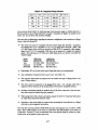
Table 2-4 provides the jumper information for the eight possible onboard DRAM memory
configurations.
Table 2-4 Onboard DRAM Memory Size Jumpering
AMOONT
SI1II1
SI1II2
SIMM3
W42
W43
W44
OK
no
no
no
open
open
open
64K
yes
no
no
short
open
open
1281(
yes
no
no
open
short
open
256K
yes
no
no
short
short
open
512K
yes
yes
no
open
open
short
640K
yes
yes
yes
short
open
short
704K(*)
yes
yes
yes
open
short
short
7681(**)
yes
yes
yes
short
short
short
Default: ei ther 256K, 512K, or 640K, depending on whether
1, 2, or 3 SIMM DRAM modules are installed.
(*) NOTE:
(**)
Do not use with EGA/VGA video controller.
NOTE:
7681( option also requires the EGA/VGA video
i .e. j~rs 1119 and 1131 RlJSt be on. Also, no
video controller can be present.
mode,
2.3.2 Math Coprocessor (J10)
The Little Board/PC does not support the use of a math coprocessor. The connector at no
was originally intended for direct connection to an NEC uPD72191. but this device was
canc~led by NEC.
Caution
Do not connect an 8087 at
Ie may result.
no. as damage to both the
board and the
Jumper option.l£JQ. corresponds to "switch 2" of a standard PC motherboard. and indicates
whether an 8087 math coprocessor is present in the system. This jumper is shorted by a trace
on the board. which indicates that a coprocessor is not present.
2-6
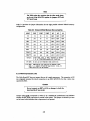
2.3.3 Byte-Wide Memory Sockets
The Little Board/PC has two onboard byte-wide memory device sockets that can accommodate a variety of EPROM and nonvolatile RAM (NOVRAM) devices, used for simple program storage or as "Solid State Disk" (SSD) drives.
Some of the byte-wide devices that can be used in these sockets are shown in Table 2-5 and 26, along with the jumpering required to support each type of device. The NOVRAM cartridges described in the table connect with a short ribbon cable (Dallas P /N DS9000) to a
byte-wide socket: UI5 or U26. Devices used in these sockets must be 300 oS (or faster).
Direct Program Access
The memory devices installed in UI5 and U26 can be accessed directly by your application
software, provided the program knows about them.
The byte-wide memory sockets reside at the following memory addresses:
•
•
U15 is at FOOOOh
U26 can start at any of the following addresses, depending on the type of device installed
and the setting of the socket configuration jumpers (see Table 2-5):
. EOOOOh
E8000h
ECOOOh
EEOOOh
Through a technique known as a "ROM-BIOS extension", it is possible to have the system run
its entire application from byte-wide socket memory devices, instead of from disk drives. This
is discussed in Ampro application note AAN-8702.
Solid State Disk (SSD) Drives
The optional Ampro Solid State Disk (SSD) Support Software, allows you to configure a
Little Board/PC system to boot, operate, and even store data using one or two EPROM
and/or NOVRAM solid-state "drives" under control of the DOS (version 3.3 or later) operating system. No custom programming is required, other than use of the development tools
provided in the SSD Support Software. Using the Ampro SSD software, the byte-wide sockets can serve as individual SSD drives, or they can be combined into one larger drive. SSD
drives can be used along with normal (floppy and hard disk) drives. Ampro's SSD Expansion
Board provides additional SSD sockets.
Based on these devices, some of the configurations possible using the Ampro SSD support
are:
•
Single EPROM Drive: -- U15 alone, or U15 combined with U26, as a bootable EPROM
drive. Up to I28K bytes capacity results from one socket, or 256K bytes if the two are
combined.
•
One EPROM drive, and one NOVRAM drive: -- UI5 as a boot able EPROM drive
(I28K bytes capacity), and U26 as a NOVRAM cartridge drive (up to 5I2K bytes capacity).
2-7
•
Two Independent NOVRAM drives: -- U15 as a bootable NOVRAM cartridge drive,
and U26 as a second NOVRAM cartridge drive (each drive up to 512K bytes).
•
One COIDbined NOVRAM drive: -- U15 plus U26 combined to form a single boatable
NOVIt.A..M Gartridge drive (up to 1 megabyte in eapacity).
Byt.Wlde Socket Configuration
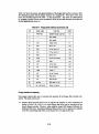
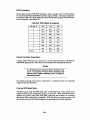
If the U15 or U26 memory sockets are used, they must be confIgured by means of jumpers
for device type, size, and the starting memory address desired. The supported memory devices and corresponding jumper settings are shown in Tables 2-5 and Table 2-6. The starting
address for U15 is FOOOOh, regardless of device type or size, while U26 can be set to start at
several addresses.
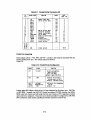
Table H. U26 Device Jumperlng
SIZE
DEVICE TYPE
(BYTES)
TYPICAL
DEVICE
ADDRESS
W35
W36
W37
W38
W45
8K
Norma l EPROM
2764
EOOOOh
open
short
short
open
open
8K
Normal EPROM
2764
ESOOOh
short
short
open
open
1/3
8K
Norma l EPROM
2764
EEOOOh
open
short
open
open
1/3
16K
Normal EPROM
27128
ECOOOh
short
open
open
1/2
113
321C
Norma l EPROM
27256
EOOOOh
open
short
short
1/2
1/3
321C
Norma l EPROM
27256
ESOOOh
short
open
short
1/2
113
64K
Norma l EPROM
27512
EOOOOh
short
short
short
1/2
3/5
128K
Page-8Cildr EPROM
27011
EOOOOh
open
short
short
2/3
2/4
8K
28-Pin SRAM
6264
EEOOOh
open
short
open
2/3
open
32K
28-Pin SRAM
62256
EOOOOh
open
short
short
2/3
4/6
32K
28-Pin SRAM
62256
ESOOOh
short
open
short
2/3
4/6
32K
to
512K
NOVRAM cartridge
DS1217x
EOOOOh
open
short
short
213
4/6
None
-----
... ----
open
open
open
open
open
OK
Note
When a byte-wide memory device is enabled, its memory
address space is unavailable for use by other devices on
the PC bus. A byte-wide socket must be marked as "disabled" (jumpers W3S-W38, w4f "open") before its memory
space can be used for other purposes.
2-8
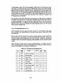
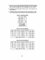
Table H. U15 Device Jumpering
SIZE
DEVICE TYPE
(BYTES)
TYPICAL
DEVICE
W12
W13
W14
W15
W16
W41
W8
81(
No....' EPRat
2764
short
open
short
open
open
2/3
short
32K
No.... l EPRCJII
27256
short
open
short
short
open
2/3
open
1281(
Page-acidr EPRCJII
27011
short
open
short
open
short
2/3
open
81(
28-Pin SRAM
6264
short
open
open
open
short
open
short
32K
28-Pin SRAM
62256
short
open
short
open
short
1/2
open
2.3.4 Battery-Backed Clock Module
An Ampro SmartClock battery-backed real time clock module can be plugged into any of the
board's three 28-pin memory option sockets (U15, U21, or U26).
If a memory device is also required in the socket used for the clock option, it can be plugged
directly into the 28-pin socket on the clock module. When this is done, the memory device is
accessed as though the clock option is not present.
A software utility is provided with the SmartOock option which can be used to initialize the
clock module for correct ~te and time, as well as to automatically set the DOS system clock
from the hardware real time clock on system powerup.
2.3.5 Video Display Mode Jumperlng
No matter what type of video display controller is used, two jumper options (W19 and W31)
on the board must be properly confIgured to indicate the desired video mode to the ROMBIOS. Table 2-7 shows the video display mode jumper settings.
Table 2-7. Video Display Mode
VIDEO MODE
W31
W19
EGA/VGA
short
short
640 X 200 CGA
short
open
320 X 200 CGA
open
short
Monochrome (SO X 25)
open
open
W19 and W31 correspond to switches 5 and 6 of a standard PC motherboard, and are used to
specify the powerup default of the video display controller. Not that the EGA/VGA video
mode (W19, W31 both on) must be set when a memory conftguration of 768K is to be used,
as described. elsewhere in this chapter.
Refer to the video controller's technical manual for its proper jumper settings.
2-9
2.3.6 I/O Wait State Option
A timing limitation in the original NEC V 40 microprocessors used in the Little Board/PC
required several wait states to be inserted on all I/O cycles. The NEC V40 microprocessors
now shipping no longel lequire the wait states. A jumper, W48, controlS whether the walt
states are enabled or disabled, as shown in Table 2-8.
Table 2-1. I/O Wait States
WAIT STATE
PINS
Disables Automatic 1/0 Wait Stetes.
Actual nunber of I/O wait
stetes is detef'llli ned by the
internel wait state generator
(use Ampro's SETWAIT utility)
1/2
Enables Automatic I/O Wait States.
Weit states are autalBtically
inserted on ell 1/0 cycles.
2/3
To ensure compatibility with older version of the Little Board/PC, the board is shipped with
automatic wait states enabled.
Note
If possible, you should reeonfigure jumper W48 to distIbk
the automatic wait states. With automatic wait states
disabled, they can be set to the desired value under software control using the SE1WAIT utility.
2.4 PERIPHERAL INTERFACE CONFIGURATION AND CONNECTIONS
This section discusses the interface requirements of the board's external device interface
connectors. Connector pinouts, signal definitions, device characteristics, and jumpering
information is included.
2.4.1 Utility Connector - J4
A single 10 pin connector (J4) provides four functions: Speaker, System Reset, Power Indicator LED, and auxiliary power to the PC Expansion Bus connector (J9). The pinout and signal
defmitions of the Utility Connector are shown in Table 2-9. Note that the power connections
indicated are not required for operation of the Little Board/PC, and are only used to supply
power to the pins indicated on the PC Expansion Bus connector.
2-10
Table 2-9. Utility Connector (J4)
PIN
SIGNAL NAME
FUNCTION
1
2
Audio return
Audio
+5 volts through 33 ohms
Speaker signel
3
GrOU'ld
RESET
To one side of Reset switch
To other side of Reset switch
LED Cathode
LED Anode
GrOU'ld return
Current source
GrOU'ld
+12V
·5V
·12V
Grcxnf return
To J9 pin 19
To J9 pin 15
To J9 pin 17
4
5
6
7
8
9
10
Speak..
The board provides a PC compatible speaker output on two pins of the Utility Connector.
The speaker signal is buffered by a transistor amplifier to provide approximately .1 watt of
audio power to an external speaker. Typically a small general purpose 2 or 3 inch diameter
permanent magnet speaker with an 8 ohm voice coll is used.
Speaker tones can be generated either by directly "bit~banging" the speaker control port or by
setting timer 2 to a desired frequency tone and enabling the tone with an enable port. See
Chapter 4, or a PC technical reference manual, for additional programming detaUs.
System Reset
Two pins of the Utility Connector provide for the connection of an external
momentary switch to manually ~ert a system reset signal.
normally~open
Power Indicator LED
Two pins of the. Utility Connector provide for the connection of an external power indicator
LED device. 15 rnA of sourced current is available ( + 5V through 330 ohms).
PC Bus Power Option
Five pins of the Utility Connector allow the sourcing of + 12VDC, ~5VDC, and ~12VDC for
use by devices connected to the board's PC Expansion Bus connector (J9). The Little
Board/PC does not itself require these voltages.
2~11
2.4.2 Keyboard - J5
A PC (or XT) compatible keyboard can be connected to the board's keyboard port via the 6pin connector, J5. Normally, PC keyboards include a cable which terminates in a male 5-pin
DIN plug for connectiOU-to a PC. Table 2 10--gives-the--baartl's-keyboard connector-pinourand signal definitions, and includes corresponding pin numbers of a normal PC DIN keyboard connector.
Note
"Ar keyboards are not compatible with PC (or XT)
keyboards, and may not be used with this interface.
Table 2-10. Keyboard Connector (J5)
J5 PIN
SIGNAL NAME
DIN PIN
1
Keyboard Clock
1
2
Keyboard Data
2
3
-Reset
3
4
GrCUlCl
4
5
+5V power
5
6
(no connection)
---
2.4.3 Parallel Printer Port - J6
The parallel printer connector (J6) has a pinout that allows the use of flat ribbon cable to a
standard DB25 PC printer connector.
Table 2-11 gives the printer connector's pinout and signal defInitions. The table also indicates
the pin number on the PC compatible DB25 printer connector which corresponds to each of
the board connector's pins. Note that the pin numbering convention for the board's header
connector differs from that of DB25 connectors, even though direct connection with flat
ribbon cable is possible. To clarify this, each signal's corresponding DB25 connector pin
number has been included in the table.
Note
Be sure not to exceed approximately 10 feet of total cable
length between the board's connector and the printer.
Table 2-11. Parallel Printer Connector (J6)
J6
PIN
1
3
5
7
9
11
13
15
17
19
21
23
25
2
4
6
8
10,12,
14,16,
18,20,
22,24
SIGNAL NAME
FUNCTION
Sample input data
LSB of printer data
IN/ruT
DB25
CONN. PIN
1
2
3
4
5
6
7
8
9
10
11
12
13
14
15
16
17
18-25
-DS
Data 0
Data 1
Data 2
Data 3
Data 4
Data 5
Data 6
Data 7
-ACK
BUSY
PAPER END
SELECT
AUTOFD
-ERROR
-INIT
SELECT
MSB of printer data
Character accepted
Cannot receive data
Out of paper
Ready to receive data
Autofeed
Printer error
Initialize printer
Select printer
out
out
out
out
out
out
out
out
out
in
in
in
in
out
in
out
out
GND
Signal ground
---
:
:
:
:
:
:
Printer Port Jumpering
Three jumper options -- Wll, W46, and W47 -- pertain to the functions associated with the
board's parallel printer port. The various options are shown in
Table 2-12.
Table 2-12. Parallel Printer Configuration
JUMPER
SIGNAL
FUNCTION
W11
To ASIC1
Selects 1/0 address.
open: 378-37Fh
short: 3BC-3BFh
default: open (378-37Fh)
W46
1447-1
1447-2
1447-3
IRQ7
Connects the on-board
printer port to IRQ 7
Default: shorted (trace)
V40 SRDY
Handshake Out
-INIT
V40 Serial Port handshake
option.
Default: 1/2
Jumper option Wll allows a choice of two I/O port addresses for the printer port: 378-37Fh,
or 3BC-3BFh. Normally, the DOS LPT1 device has address 378-37Fh; however, the ROMBIOS scans both choices and will install the flrst one it flnds as LPT1 regardless of which
option has been conflgured. The printer port should normally be conflgured for 378-37Fh
(Wll unshorted), unless another parallel port interface is present on the PC bus.
2-13
A second jumper option, W46, has been provided to allow the use of the printer port interrupt (IRQ 7) as an extra interrupt on the PC Expansion Bus if you do not require interruptbased operation of the board's parallel printer port. The print functions in the board's ROMBIOS do not use the interrupt. However, some PC applications (e.g. spoolers) might require
printer interrupts, SO-it-is-recommetKled--that you leave this interrupt connected wdess you aJ e
certain it is will not be needed. To free IRQ 7 for use on the PC Expansion Bus, cut the trace
shorting W46 (on the non-component side of the board). IRQ 7 will now be available on the
PC Expansion Bus, at J9 pin B21.
The third jumper option, W47, allows the use of the printer port -INIT signal as a Handshake
Out signal for the V40 serial port. If that option is employed, the printer port must either not
be used for anything else, or must be used in a manner that does not result in erroneous
handshake signal usage. As indicated in the table, shorting pin 1 to pin 2 is the normal confIguration, which results in the Handshake Out signal being generated by the V40's internal
serial controller handshake logic.
2.4.4 PC Compatible Serial Port - J3
The PC compatible serial port appears at header connector J3. Three RS232C output signals
and fIve RS232C input signals facilitate connecting a broad range of serial devices to the
Little Board/PC.
This port can be used for connection of a printer, modem, terminal, or other serial device.
The main interface consideration is that the device be RS232C compatible. Printers and
modems generally require handshaking in one or both directions. Consult the serial device's
installation manual for information regarding possible handshake and other interface considerations.
Table 2-13 gives the board's connector pinout and signal dermitions. In addition, the pins to
which each signal should be wired for compatibility with the COM port external serial connectors of PC's (DB25) and ATs (DB9) are also indicated.
Table 2-13. PC Serial Port Connections (J3)
IN/aJT
DB25
PIN
DB9
PIN
Data Carrier Detect
in
8
1
DSR
Data Set Ready
in
6
6
3
RXD
Receive Data
in
3
2
4
RTS
Request To Send
out
4
7
5
TXD
Data OUtput
out
2
3
6
CTS
Clear to Send
in
5
8
7
DTR
Data Terminal Ready
out
2D
4
8
RI
Ring Indicator
in
22
9
9
GND
Signal Gr<l'.Wld
.-
7
5
10
---
(no connection)
--
--
--
PIN
SIGNAL
NAME
1
DCD
2
J3
FUNCTION
2-14
PC Serial Port Jumperlng
Three jumpers (W17, W18, and W20) can be used to modify the I/O port address (3F8-3FFh
or 2F8-2Ffb) and interrupt usage ORQ3 or IRQ4) of the PC Serial Port. Jumper W20 selects the port's I/O port address, while interrupt channel selection is made using either W17
or W18. Refer to Table 2-14 when making serial channel selection.
Nota
Normally, the DOS COMt device bas address 3F8-3FFh
and interrupt IRQ4; however, the ROM-BIOS scans both
choices and will install the first one it finds as COMt
regardless of which option has been configured.
Tabla 2-14. PC Serial Port Configuration
I/O ADDRESSING
INTERRUPT
W17
W18
W20
3F8h thru 3FFh
IRQ4
short
open
open
2F8h thru 2FFh
IRQ3
open
short
short
short
open
open
Default:
2.4.5 V40 Serial Port - J2
A non-standard RS232C serial port, based on the V40's internal serial controller function,
appears at connector J2. This port can be used for connection of many types of RS232C
serial devices. However, because this port is not compatible with the serial ports normally
used in PC's, off-the-shelf communications programs cannot be used without modification.
This port requires the use of customized or modified software, unless it is to be used as a
serial console device (see Chapter 3). One additional limitation of the V40 serial port is that
it cannot be used in an interrupt driven mode, unless the board's keyboard interrupt is not
required (see Chapter 4).
A single active handshaking signal in each direction is available, for use with printers,
modems, and other devices, to control the flow of data. Consult the external serial device's
installation manual for information regarding appropriate handshake protocols, and other
interface considerations.
Table 2-15 gives the board's connector pinout and signal dermitions. In addition, the pins to
which each signal should be wired for compatibility with a subset of the COM port external
serial connectors of PC's (DB2S) and ATs (DB9) is also indicated. One output signal (12-5,
DTR) provides a means of sending an EIA TRUE to the attached device, if needed. In some
applications it may be necessary to connect either the input handshake signal (CTS), output
handshake signal (RTS), or output EIA True signal level (DTR) to different pins of either
the DB2S or DB9 connectors than those shown in the table.
2-15
Table 2-15. V40 Serial Port Connections (J2)
J2
Pin
SIGNAL
FUNCTION
IN/OUT
OB2S
PIN
OB9
PIN
NAME
1
RXD
Receive Data
in
3
2
2
RTS
Henclshake OUt
out
4
7
3
TXD
Transmit Data
out
2
3
4
CTS
Henclshake In
in
5
8
5
OTR
EIA True
out
20
4
6
GND
Si 11M l GrOWlCi
---
7
5
V40 Serial Port Jumperlng
The only jumper option pertaining to the board's V40 serial port is the selection of the source
of the Handshake Out signal (RTS). W47. a 3 pin jumper group. allows the Handshake Out
signal to be driven by either the V40's serial controller handshake output logic. or by the
printer interface's -INIT signal.
As shipped from the factory. this signal is connected to the handshake signal. (SRDY; V40 pin
36) generated by the serial controller within the V40 microprocessor. As utilized by the
ROM-BIOS. the V40's handshake signal automatically goes true when the receive buffer is
ready to receive data. and false when the receive buffer is full.
Alternatively. the Handshake Out signal source can be jumpered to the printer port -INIT
signal. This provides a signal source which is completely under software control. but is only
useful if the printer port will not be used. or if the applications running on the board will not
.
use the -INIT signal when using the printer port.
To select the V40's handshake output logic. insert a shorting block between W47 pins 1 and 2;
to use the printer -INIT signal. short pins 2 and 3. The default is normall""Yi'ii V4O's handshake output signal.
2.4.6 Floppy Disk Interface - J8
The board's floppy disk controller subsystem and ROM-BIOS support one or two floppy disk
drives in any of the standard DOS formats shown in Table 2-16.
2-16
Table 2-16. Supported Floppy Formats
Capacity
Tracks
Drive Size
Data Rate
DOS Version
360K
40
5-1/4"
250 KHz
2.1+
1.2M
80
5-1/4"
500 KHz
3.0+
720K
80
3-1/2"
250 KHz
3.2+
1.44M
80
3-1/2"
500 KHz
3.3+
~ you can see from Table 2-16, nearly any type of soft-sectored, single or double-sided, 40 or
80 track, mini or micro floppy disk drive is usable. Naturally, the higher the quality of the
drives you use, the better your system's reliability.
Here are some considerations regarding the selection, conftgUfation, and connection of floppy
.
drives to the Little Board/PC:
•
The drives used must be compatible with the board's floppy disk interface. In general,
any standard PC or AT compatible 5-1/4" or 3-1/2" floppy drive will work. 7201(, 1.2M
or 1.44M floppy drives used must provide an IBM PC/AT compatible "disk change"
signal. Any 5-1/4" AT compatible 1.2M drive can be expected to supply the required
signal. The following 3-1/2" 720K and 1.44M floppy drives are known to provide the
required signal:
Brand
Fujitsu
Teac
Panasonic
Mitsubishi
720KDrive
M532K-19A
FD-235-F-l00U
JU-253-09P
MF353C-12UJ
1.44MDrive
M2537K-19A
FD-235-HF-I0I-U
JU-257-14PF
MF-355C-12UJ
•
High quality, DC servo direct drive motor floppy disk drives are recommended.
•
Any combination of supported drives can be used. See Table 2-14.
•
The computer board must be jumpered for the number and type of floppy drives to be
used. (Details follow.)
•
The drives must be jumpered to the second drive select. Use a floppy cable with a
segment of wires twisted, as is the usual practice in PC and AT compatible systems.
•
Resistive terminations should be installed only on the drive connected to the last interface cable connector (farthest from the computer).
•
When using drives with a Head Load option, jumper the drive for "head load with motor
on" rather than "head load with drive select."
•
Sometimes a thin metal shield is required when mounting the board directly to a floppy
drive due to electromagnetic interactions.
Note that the Little Board/PC's ROM-BIOS provides dual-capacity use of 1.2M or 1.44M
drive: that is, 360K floppies can be read in a 1.2M drive, and 720K floppies can be read in a
1.44M drive. However, it is not recommended that a low-density floppy be written in a highdensity drive, as incomplete erasure may occur.
2-17
Table 2-17 shows the pinout and signal defmitions of the floppy disk interface connector (J8).
J8 is identical in pinout with the floppy connector of a standard PC. Note that in a PC, both
drives are normally jumpered the same -- as the second drive. The drives are differentiated
by swappina a group of seven wires (conductors 10-16) in the cable-between the board andthe fIrst physical drive (drive A).
Table 2-17. Floppy Disk Interface Connector (J8)
PIN
2
SIGNAL NAME
-RPM/-RWC
IN/ClJT
FUNCTION
Speed/Prec~
(option)
out
(Not used)
--
(Not used)
--
6
-----
8
-lOX
Index Pulse
in
10
-M01
Motor
out
12
-DS2
Drive Select 2
out
14
-DS1
Drive Select 1
out
16
-M02
Motor
out
18
-DIRC
Direction Select
out
20
-STEP
Step
out
22
-w
Write Data
out
24
-WE
Write Enable
out
26
-TRKO
Track 0
in
28
-WP
Write Protect
in
30
-ROD
Read Data
in
32
-HS
Head Select
out
34
pull up
330 ohms to +5V
---
4
1-33
(all odd pins)
On
On
1
2
Signa l grOl.llds
Floppy Interface Jumpering
Nme jumper options allow you to customize the operation of the floppy disk controller subsystem. The main concerns are:
•
Jumpers W32 and W33 must be set to indicate the quantity of drives connected, as
shown in Table 2-18. Only 1 or 2 actual floppy disk drives can be interfaced by the
board's floppy controller. However, when using the Ampro SSD Support Software, two
additional SSD drives (emulating additional floppy drives) can be supported in addition
to the two actual floppy disk drives, so the choices of 3 or 4 apply in this case.
2-18
•
Be sure to also set the four drive type jumpers (W26-W29) to specify what kind of floppy
disk drives to be used, as indicated in Table 2-19 and Table 2-20. Table 2-19 applies to
Drive A. and Table 2-20 applies to Drive B. Any combination of two drives is allowed.
•
On boards that currently ship, jumper W49 must be shorted. (This configuration is the
default as shipped.)
•
If nothing is connected to the SCSI connector (J7) insert a shorting block on J7 pins 1
and 2 to disable attempted system boot from SCSI. This speeds up booting from floppy.
Table 2-18. Floppy Drive Quantity
W33
W32
DRIVES
short
short
1
open
short
2
short
open
3 (*)
open
open
4 (*)
Default: 2 drives
(*) Not supported,
except with Ampro's
SSD Support Software.
Table 2-19. Drive A Type Selection
CAPACITY
TRACKS
DRIVE SIZE
DATA RATE
DOS VERSION
W26
W28
360K
40
5-1/4"
250 KHz
2.1+
open
open
1.2M
80
5-1/4"
500 KHz
3.0+
open
short
nOK
80
3-1/2"
250 KHz
3.2+
short
open
1.44M
80
3-1/2"
500 KHz
3.3+
short
short
open
open
Default: 36OK, 5-1/4" drive
Table 2-20. Drive B Type Selection
CAPACITY
TRACKS
DRIVE SIZE
DATA RATE
DOS VERSION
W27
W29
360K
40
5-1/4"
250 KHz
2.1+
open
open
102M
80
5-1/4"
500 KHz
3.0+
open
short
nOK
80
3-1/2"
250 KHz
3.2+
short
open
1.44M
80
3-1/2"
500 KHz
3.3+
short
short
open
open
Default: 36OK, 5-1/4" drive
2-19
Two additional options, shown in Table 2-21, allow you to alter the DMA channel and interrupt channel assignment. Changing these from the defaults is not recommended because it
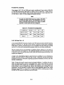
would sacrifice compatibility with the board's ROM-BIOS.
Table 2-21. Floppy Interface Options
JUMPER
SIGNAL
WS-1
WS-2
WS·3
DACK1
DACK to FDC
DACK2
DNA acknowledge chamel option.
Default: 2/3 (DACK2), via a trace.
W7-1
W7-2
W7-3
DR01
ORO from FDC
DR02
DNA request chamel option.
Default: 2/3 (DR02), via a trace
W10
IRQ6
When shorted, connects board's floppy
controller to interrupt request IRQ6.
Must be shorted if the board is equipped
with a floppy disk controller.
Default: shorted
W26W29
FUNCTION
Select floppy drive type for drives A
and B, as shown in Tables 2-19 and 2-20.
Default: all unshorted
W32
W33
PC Switch 8
PC Switch 7
Drive quantity, as shown in Table 2-18.
Default: W32 on, W33 off.
W39
PCVAL
Write precClq)enSation value. Unshorted
selects 125 nS. Shorted selects 187 nS.
Defaul t: unshorted
W40
DRV
Drive type. Unshorted selects single
speed drives. Shorted selects dual
speed drives.
Default: unshorted
W49
Must be shorted.
Default: shorted
2-20
2.5 SCSI INTERFACE - J7
The SCSI interface (17) uses a 5O-pin male header connector to interface with SCSI compatible peripherals. Table 2-22 shows the pinout and signal defmitions of this interface. Refer to
your SCSI device documentation, or the ANSI X3.131 SCSI specification (referred to in
Chapter 4) for detailed information on the signal functions. Be sure that the maximum total
SCSI bus cable length, from the board's connector to the most distant SCSI peripheral, does
not exceed 18 feet, and that the SCSI bus is properly terminated at both ends.
Note
If the SCSI interface is not needed, you should disable it
by placing a shorting block on pins 1 and 2 of the SCSI
connector (J7). When the shorting block is in place. the
system bypasses any attempt to boot from the SCSI device.
which can speed up the boot process.
Table 2-22. SCSI Interface Connector (J7)
PIN
1 • 49
2
4
6
8
10
12
14
16
18
20,22,24
25
26
28,30
32
34
36
38
40
42
44
46
48
50
SIGNAL
FUNCTION
(All odd pins)
-DBO
-DB1
-DB2
-DB3
-DB4
-DB5
-DB6
-DB7
-DBP
GrOl.l'ld
---
TERMPWR
GrOl.l'ld
-ATN
GrOl.l'ld
-BSY
-AtK
-RST
-MSG
-SEL
-C/O
REQ
-I/O
2-21
Signal grounds
ta B·t 0 (LSB)
1
2
3
4
5
6
I
I
7 (MSB)
Data Parity
Signal Ground
(Not used)
Termination +5VDC
Signal Ground
Attention
Signa l GrOl.l'ld
Busy
Transfer Acknowledge
Reset
Message
Select
Control/Data
Transfer Request
Data direction
o
2.5.1 Normal Use of SCSI
The board's SCSI bus interface can serve a variety of purposes, including connection of hard
disk controllers, tape controllers, text scanners, and printer and communications servers.
Support is provided by the board's ROM-BIOS for booting of DOS from a SCSI de'Ace such
as a hard disk. Virtually any device compatible with the SCSI Common Command Set for
direct access devices can be used through the ROM-BIOS support. Some examples of direct
access SCSI devices that can be accessed as DOS drives are hard disk drives, magnetic bubble
drives, high density floppy drives, and some tape drives.
The Little Board/PC comes with a diskette containing software utilities for normal DOS
operation using hard disks and other SCSI direct access devices. A powerful SCSI formatting
utility is included that allows low-level formatting, changing the interleave, and mapping out
bad sectors. Refer to Chapter 4 for information on software ~tup and drive preparation.
PC-DOS version 3.x requires that drives larger than 32 megabytes be partitioned into more
than one "partition", while DR-DOS, MS-DOS 4.x, and PC-DOS 4.x allow such drives to be
used without partitioning. Under PC-DOS or MS-DOS 3.x, each drive can be logically partitioned into as many as four partitions, 32 megabytes or smaller, allowing the use of physical
drives as large as 128 megabytes. DR-DOS, MS-DOS 4.x, and PC-DOS 4.x support a
maximum drive size of 512M bytes.
There are several other types of SCSI devices besides direct access devices. SCSfs additional
device types include sequentk1l access devices (e.g. tape), printer devices, read-only devices (e.g.
CD-ROM), and processor devices (e.g. CPU's). In general, these other device types require
special application programs, utilities, or driver software for use.
Hard disk support for operating systems other than DOS mayor may not be automatically
available through the board's ROM-BIOS resident hard disk driver. This depends on whether the operating system in question uses BIOS calls exclusively for the hard disk function, and
whether the operating system has any special ROM-BIOS constraints (such as re-entrancy).
Some operating systems -- multitasking ones in particular such as Unix -- interface directly
with the hardware (e.g. attempt to directly program a bus hard disk controller) and bypass
BIOS. In those situations, the operating system must be modified to add an appropriate SCSI
hard disk driver to use the to take advantage of the board's SCSI interface.
2.5.2 The Ampro SCSI/BIOS
Through the universal bus interface and command protocols offered by SCSI, it is possible to
connect a wide variety of mass storage devices to a computer system with virtually no changes
to system software. To this, Ampro has added a further layer of universality: the
SCSI/BIOS.
As its name implies, the SCSI/BIOS consists of a set of low level functions which have been
incorporated into the ROM-BIOS to provide a hardware independent interface between
system software and peripheral devices connected to the SCSI bus. The advantage of the
Ampro SCSI/BIOS is that programmers can write software that uses devices connected to
the SCSI bus without having to be concerned with the details of operating the board's SCSI
bus interface. Also, software can be ported to the Little Board/PC from other hardware
environments much faster due to the presence of the SCSIIBIOS, and with less difficulty and
risk.
2-22
The board's SCSI interface, and the Ampro SCSIIBIOS within the board's ROM-BIOS are
discussed in greater detail in Chapters 4 and 5. In addition application note AAN-8804, available from Ampro, provides details of the SCSIIBIOS functions available to programmers.
2.5.3 Simple Bidirectional If0
When the board's SCSI bus is not needed for interfacing to standard SCSI devices, it can be
used instead as a general purpose digital input/output port. The SCSI bus then becomes a
set of programmable I/O signals, with TIL signal levels and open collector output drivers
capable of sinking 48 mAo In this case, sixteen SCSI bus signals can be used; of these, nine
are capable of bidirectional use, and seven are input-only.
The available SCSI port output signals can be "hit-banged" (i.e. software activated) to generate a wide variety of signal timings and operations. For example. it is even possible to interface with optically isolated AC and DC input and output modules, and to a number of off-theshelf data acquisition and control interfaces.
Ampro application note AAN~1 discusses a typical non-SCSI application. Refer also to
Chapters 4 and 5 for typical system configuration information, and for technical information
about the board's SCSI bus interface.
2.5.4 SCSI Interface Configuration
Several items associated with the board's SCSI interface should be conftgUl'ed according to
your system needs:
SCSI Bus Termination
Three 8-pin 220/330 ohm SIP resistor networks (RP4, RP5, and RP6) provide bus termination. The termination networks should be present on two, and only two, SCSI bus devices.
An improperly terminated SCSI bus may interfere with normal system operation due to
indeterminate signal levels.
Note
Be sure that the SCSI termination networks are oriented
in their sockets so that pin 1 of each SIP network, generally marked with a dot, is at the top end of the board as
shown in Figure 2-1.
Internally, pins 2-7 of the SIP networks have 220 ohm resistors connected to + 5 volts (pin 8),
and 330 ohm resistors connected to ground (pin 1).
Note that the SCSI Bus terminatiOn networks consume significant power (.8 watt). If power
consumption is critical, consider having the bus termination external to the board, and externally powered.
2-23
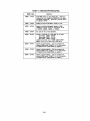
SCSIID Jumperlng
Three jumper pin pairs (W23-W25) normally are used to provide a three bit SCSI Initiator
10, for use by the board's ROM-BIOS and other support software. The jumper assignments
are shown in-Table 2-23. These jumper pins can be used for other purposes if tbe SCSI interface is not required. (See Chapter 5).
Table 2-23. SCSI Initiator ID Jumpering
SCSI Bus ID
W25
W24
W23
0
short
short
short
1
short
short
open
2
short
open
short
3
short
open
open
4
open
short
short
5
open
short
open
6
open
open
short
7
open
open
open
open
open
open
.
Default:
7
External Termination Power Option
A jumper option (W4) allows the connection of +5 volts termination power to the SCSI bus
TERMPWR signal (pin 26). Please observe the following caution regarding this function:
Caution
No termination power protection diode is provided on the
board. Consequently, W4 IIIIUt NOT be installed if any
other bllS devke suppliu terminatioII power, or damage to
1M boanllflay tesrdL
The default jumpering of this option is unshorted; i.e., termination power is not normally
supplied by the Little Board/PC.
Enhanced SCSI Speed Option
The SCSI support within the ROM-BIOS offers a "SCSI Halt Mode" option, which can be
enabled by shorting two configuration jumpers on the board. When SCSI Halt Mode is
enabled, the processor halts while SCSI DMA read/write data transfers are occurring,
allowing the DMA channel full bus bandwidth. SCSI Halt Mode can provide as much as 25
percent improvement in SCSI data throughput rate, depending on the specific application.
2-24
To enable the SCSI halt mode, install shorting jumpers at WI and W6 on the Little
Board/PC. WI is located between Ul and SIMM2; W6 is located between U2 and U6 (refer
back to FtgUl'e 2-1). When these two jumpers are left off, SCSI Halt Mode is disabled. The
default configuration, as shipped, is SCSI Halt Mode disabled.
Alternate DMA Channel Option
The SCSI interface can be configured to use either DMA channel 1 or 3 for data transfer
control. DMA Channel 3 corresponds to a standard PC's fixed disk adapter, and is used as
the default by the board's SCSI/BIOS. You can alter these assignments relative to the defaults, but this will sacrifice SCSI/BIOS and SCSI utilities compatibility. These SCSI interface conftgUl'ation options are shown in Table 2-24.
Table 2-24. SCSI Interface Option Jumpers
JUMPER
W1
SIGNAL
FUNCTION
PCTC
Connects DNA END (TC) signal to
53C80's -EOP input.
Default: unshorted.
W2-1
W2-2
W2-3
DRQ3
DRQ from 53C80
DRQ1
DNA request chamel option.
Default: 1/2 (DRQ3), via a trace.
(W2-1 is at top.)
W3-1
W3-2
W3-3
DACa
DACK to 53C80
DACK1
DNA acknowledge chamel option.
Default: 1/2 (DACa), via a trace_
(W3-1 is at top.)
W4
Term Power
Provides +5 volts termination power
to pin 26 of the SCSI Bus.
Default: unshorted.
W6
53C80 IRQ
Connects 53C80's interrupt output
to PC bus IRQ5.
Default: unshorted
No termination power protection diode is provided on the board.
W4 nust NOT be installed if any other bus device supplies
termination power, or board damage may result!
2-25
2.6 PC EXPANSION BUS - J8
A PC compatible expansion bus appears at connector J9, except that it is brought out to a
healkr COMeCtor, rather than edgecard connectors.
The board's PC Expansion Bus connects to the ftrst 62 pins of J9; the two additional pins of
J9 (A32, B32) offer additional ground signals, for enhanced system reliability. PC Expansion
Bus connector pinouts are given later in this chapter.
Table 2-25 shows the pinout and signal functions of the signals on the board's PC Expansion
Bus and MiniModule headers. Further information about these signals is available in numerous pUblications, including the IBM technical reference manuals for the PC computer, and
from the reference documents listed in the beginning of Chapter 4.
Note that the board's PC Expansion Bus and MiniModule connector pins are numbered differently from the other header connectors on the board, so that they correspond to the
scheme normally used on the PC Expansion Bus. Speciftcally, rather than being designated
numerically (1, 2, 3, etc.) the signals of the PC Expansion Bus are designated aJp/ul-numericaJ{y (A!, A2, "'J Bl, B2, ..., etc).
PC Expansion Bus signals are buffered on the board and provide approximately 4 mA source
and sink currents for peripheral cards, with TIL compatible signal levels at a logic 'ow" level
of 0.4 Volts.
2.6.1 Onboard MiniModule Header and Bus Expansion
An important feature· of the Little Board/PC is its onboard MiniModule header. A header
connector at 19 provides a PC Expansion Bus interface for use with one of Ampro's 3.6" x 3.8"
expansion MiniModules. When installed on J9, the onboard expansion module ftts within the
Little Board/PC's space envelope. The onboard expansion module provides a bus passthrough connector, allowing additional external bus expansion when the module is installed.
Several options are available for mounting multiple MiniModules on the Little Board/PC:
•
Stacker/MM -- Allows two MiniModules to be stacked together and mounted as a
single unit.
•
StackPIane/MM -- Provides two expansion bus header connectors for mounting MiniModules on a Little Board form-factor board. When used with the Stacker/MM, up to
four MiniModules can be attached. The SSD Expansion board also offers two expansion
bus header connectors for mounting MiniModules.
Ampro currently offers several display coQtroUer MiniModules which offer a wide variety of
standard PC and AT video modes, including VGA, EGA, CGA, MDA, and Hercules display
compatibility, on CRT monitors, LCD panels, and electroluminescent (EL) panels. Ampro
also offers additional MiniModules, including serial/parallel interfaces, modems, etc.
Contact Ampro for information on additional MiniModules.
2-26
2.6.2 Using Standard PC Bus Cards
There are several options available from Ampro which allow you to add expansion cards to
the Little Board/pC system:
•
StackPlane/PC Expansion Adapter -- a board having the identical dimensions and
mounting points as the Little Board/PC. This adapter converts a single short (8 inches
or less) PC add-on card to the Little Board form factor. The StackPlane/PC adapter
piggy-backs above or below the Little Board/PC and connects to the PC Expansion Bus
by means of a short ribbon cable. Several StackPlane/PC adapter assemblies can be
stacked.
•
MiniBackplane/PC -- two-slot PC bus passive backplane with PC bus header for cable
connection to the PC Expansion Bus header on the Little Board/PC.
•
PC Backplane Adapter -- small circuit card which plugs into one edgecard connector on
any PC bus passive backplane, and provides a PC bus header for cable connection to the
PC Expansion Bus header on the Little Board/PC.
•
Cable-Mount Edgecard Sockets -- 62-pin edgecard connectors can be used to construct
a ribbon cable which can connect the Little Board/PC's PC Expansion Bus directly to a
PC plug-in expansion card using ribbon cable only. The edgecard sockets are available
from
PCD Connectors
Winchester, MA
(617) 721-1280
RF31-2582-5 (62-conductor edgecard socket)
Contact an Ampro sales representative for further information on these optional bus expansion products.
2.6.3 Expansion Bus Cable Considerations
Here are· several points regarding the use of the board's AT Expansion Bus:
•
Cable Length -- Keep the ribbon cable used as short as possible. Expansion bus cables in
excess of six inches can result in reduced system reliability. We recommend:
-- For cable lengths up to 6 inches, use a high quality ribbon cable, such as 3M part
number 3365/64 (64 conductor).
-- For cable lengths between 6 and U inches, use a high quality ribbon cable with ground
plane, such as 3M part number 3353/64 (64 conductor).
-- Cable lengths in excess of U inches are not recommended.
2-27
•
Backplane Quality -- Be sure to use a high quality backplane having minimal signal
crosstalk. Use of power and ground planes, and ground guard traces between bus signals is recommended
•
Reset DegUtGhing Some PC bus expansion cards have asynchronous I I L inputs that
are .especially wlnerable to cable noise and crosstalk. In particular, the active high
RESET line is one to watch out for. If this signal is found to be susceptible, a 200pf to
SOOpf capacitor connected between the RESET signal and ground can be used to prevent false expansion card resets. This RESET deglitching capacitor is included on the
Ampro MiniBackplanes.
2.6.4 Exparislon Bus Connector Pinouts
Tables 2-25A and 2-25B indicate the pinout and signal functions of the signals on the board's
PC Expansion Bus connectors. Further information about these signals is available in
numerous publications, including the mM technical reference manuals for the PC computer,
and from the reference documents listed in the beginning of Chapter 4.
The board's PC Expansion Bus header connector (J9) pins have been numbered differently
from the other header connectors on the board, so that they correspond to the scheme
normally used on PC bus edgecard connectors. The even numbered pins correspond to the
"B" row of the PC bus; and the odd numbered pins correspond to the "A" row (e.g., J9 pin I is
labeled "BI"). The fll'St 62 pins of J9 (beginning at Al and BI) are the ones which correspond
to the 62 conductors-of the PC Expansion Bus of the PC backplane. The last two pins are
spare grounds.
Note that the Little BoardlPC does not generate + / - 12VDC or -SVDC for the PC Expansion Bus. If devices on the PC Expansion Bus require these voltages, they can be supplied to
the PC Expansion Bus connector from the board's utility connector (J4).
2-28
Table 2-25A. PC Expansion Bus Connector, A1-A32 (J9)
PIN
SIGNAL NAME
A1
A2
-I/O CH CK
D7
D6
D5
D4
D3
D2
D1
DO
I/O CH RDY
AEN
A19
A18
A17
A16
A15
A14
A13
A12
A11
A10
A9
A8
A7
A3
A4
AS
A6
A7
A8
A9
A10
A11
A12
A13
A14
A15
A16
A17
A18
A19
A20
A21
A22
A23
A24
A25
A26
A27
A28
A29
A30
A31
A32
A6.
AS
A4
A3
A2
A1
AO
GND
FUNCTION
Memory parity error
Data bit 7
Data bit 6
Data bit 5
Data bit 4
Data bit 3
Data bit 2
Data bit 1
Data bit 0
Processor Ready Ctrl
Address Enable
Address bit 19
Address bit 18
Address bi t 17
Address bit 16
Address bi t 15
Address bit 14
Address bit 13
Address bit 12
Address bit 11
Address bit 10
Address bi t 9
Address bi t 8
Address bi t 7
Address bi t 6
Address bi t 5
Address bi t 4
Address bi t 3
Address bit 2
Address bit 1
Address bi t 0
Ground
2-29
IN/OUT
in
i/o
i/o
i/o
i/o
i/o
i/o
i/o
i/o
in
out
out
out
out
out
out
out
out
out
out
out
out
out
out
out
out
out
out
out
out
out
---
Table 2-25B. PC expansion Bus Connector, B1-B32 (J9)
PIN
...
11
i3
B4
15
B6
17
B8
19
110
111
112
113
114
115
116
117
118
119
120
121
122
123
124
125
126
127
128
129
830
831
832
SIGNAL NAME
GNO
+5y.... •
IRQ2
-5V
DRQ2
-12V
NIC
+12V
GND
-MEMW
-MEMR
-row
-lOR
-DACa
DRQ3
-DACK1
DRQ1
-DACKO
CLOCK
IRQ7
IRQ6
IRgs
IRQ4
IRQ3
-OACK2
TIC
ALE
+$V
OSC
GNO
GND
FUNCTION
GrOlnS
;Jr-~-
r . . . ~ SIgna,
+5 vol ts power
Interrupt request 2
Fro. J4 pin 9
DNA request 2
Fra. J4 pin 10
(no connection)
Fro. J4 pin 8
GrOlnS
Memory Write
Memory Read
I/O Write
I/O Read
DNA Acknowledge 3
DNA Request 3
DNA Acknowledge 1
DNA Request 1
Memory Refresh
7.16 MHz clock.
Interrupt Request 7
Interrupt Request 6
Interrupt Request 5
Interrupt Request 4
Interrupt Request 3
DNA Acknowledge 2
DNA Te,..inal Count
Address Latch Enable
+5 vol ts power
14.31818 MHz clock
GrCUld
GrCUld
2-30
INIOUT
---
OUt
--in
in
---
out
out
out
out
in
out
out
in
out
out
in
in
in
in
in
out
out
out
---
out
out
out
CHAPTER 3
SOFTWARE CONFIGURATION
3.1 INTRODUCTION
This chapter provides an overview of the system features, confIgUl'ation options, and utilities
that are available under the DOS operating system. A combination of standard DOS and
Ampro-supplied utilities and drivers allows you to create a highly customized system based on
the Little Board/PC.
Assuming you have connected the Little Board/PC to a monitor, keyboard, and floppy drive
as described in Chapter 2, you should have no difficulty booting the system under DOS. You
will probably want to take advantage of the flexibility designed into the Little Board/PC
ROM-BIOS and utilities software to create a customized DOS-based installation. You can
tailor your software confIgUl'ation to a wide variety of hardware configurations, as indicated in
Chapter 2. This chapter provides a discussion of how to confIgUl'e the operating system and
utility software for many typical installations.
Some familiarity with DOS (pC-DOS, MS-DOS, or DR-DOS) is assumed. Please refer to
the appropriate IBM, Microsoft, or Digital Research DOS reference manuals for further
information on the use of the DOS operating system and its drivers and utilities. In addition,
Appendix A of this manual contains detailed descriptions of each of the Ampro Little
Board/PC driver and utility programs.
3.1.1 Conventions
In the descriptions of the use of software utilities, keyboard inputs which you will make to the
system are shown underlined. This has been done to make it easy for you to distinguish
between the computer's prompts and the operator's keystrokes. For example,
A> DIR < Enter >
means that you type "DIR" and then press the <Enter> key on your keyboard. (On some
keyboards this key may also be labeled <Return>.)
In most cases, upper and lower case letters can be used interchangeably when you supply
parameters to a program. For example:
A>SCSIPARK <Enter>
has the same effect as:
A> scsipark < Enter>
3-1
3.2 OPERATION WITH DOS
The Little Board/PC and its ROM-BIOS have been designed to allow the use of IBM PCDOS, Microsoft MS-DOS, or Digital Research DR-DOS, versions 2.x or 3.x, and PC-DOS or
MS-DOS version 4.01, as the board's operating system. Throughout this chapter, the term
"DOS" will be used to refer to any of these operating systems, except in cases where a difference in operation exists.
Caution
Many variations of MS-DOS exist which have been customized for operation on specific computer systems.
These cannot be expected to function properly on the
Little Board/PC. and should not be used. Use "IBM PCDOS". or use the "generic IBM compatible" version of MSDOS supplUddirectly by Microsoft 011 an OEM basis. if you
do not choose to use the DR-DOS operating system supplied by Ampro.
In addition to supporting the standard DOS functions, the board's ROM-BIOS internal functions are highly compatible with those of the "standard PC", allowing software which makes
direct ROM-BIOS calls to function properly, without modification.
Nearly all of the hardware ports and controllers on the Little Board/PC are identical in function with those of the "standard PC". This includes the floppy controller, keyboard port,
speaker port, PC serial port, parallel printer port, counter/timers, and interrupt controller.
In addition, the optional Ampro MinModule/VGA, MiniModule/EGA, MinModule/CGA,
and MiniModule/LCD onboard display controller modules offer the most popular PCcompatible video modes: VGA, EGA, CGA, MDA, and Hercules monochrome graphics on
either CRT or LCD displays.
Although the board's DMA controller is not totally compatible, special logic in the board's
ASIC devices in combination with support within the board's ROM-BIOS result in software
compatibility.
The board's 8250-based "PC Serial Port" can be jumpered as either the DOS "COM!" or
"COM2" port. The Parallel Printer port can be jumpered as either "LPTl" or "LPT2". These
devices, as well as the keyboard and speaker ports, are supported by the ROM-BIOS in a PCcompatible manner.
The board's non-compatible "V40 Serial Port" can be substituted as a system console port
(using the Ampro CONDRVR device driver) command, for applications which can use a
serial device for keyboard and display. Refer to the discussion of "Serial Console Option,"
presented later in this chapter.
The DOS and ROM-BIOS time-of-day clocks are supported in the usual manner. They can
be initialized automatically by a utility to the value stored in the optional battery-backed clock
module on system reset or powerup. Refer to the documentation supplied with the batterybacked clock for further details.
3-2
DOS version 3.2 (or later) is required for operation with SO-track (720K) mini- or microfloppy drives. DOS version 3.3 (or later) is needed for use with 1.44 megabyte microfloppies,
and with the optional Ampro Solid State Disk support utilities. DOS version 3 or later is
required for SCSI bard disk usage under the board's ROM-BIOS and SCSI support software.
In addition, support for hard disks larger than 32 megabytes is available under DR-DOS
version 3.4 (or later), or under MS-DOS or PC-DOS versions 4.0 (or later).
3.2.1 Configuration Options
A wide degree of system configurability is available through options provided by: (1) the
DOS operating system and its drivers and utilities; (2) the Ampro Little BoardlPC Utilities;
and (3) the Ampro SCSI Utilities.
The conftgUfation options include:
•
•
•
•
•
Console selection and setup
Parallel and Serial port selection and setup
Modem interface
A variety of floppy disk drives
A SCSI bard disk drive
Examples of how a typical system can be configured for many of these options are given in
later in this chapter.
The following section briefly summarizes the features of the software included in the Ampro
Little Board/PC utilities and drivers. Appendix A contains detailed program descriptions.
3.2.2 Uttle Board/PC Utilities OvervIew
The following drivers and utilities are contained on the Little Board/PC Utilities diskette at
this time. Actual utility names and descriptions may vary. in which case appropriate "DOC"
flies are included on the diskettes. Each of these programs are described in Appendix A of
this manual (alphabetically arranged).
•
CONDRVR.SYS -- Allows serial display/keyboard devices connected to the non-standard V 40 serial port to be used as the DOS console device.
•
PRNDRVR.SYS -- Remaps the DOS parallel printer function to the non-standard V40
serial port.
•
SElWAIT -- Sets CPU wait states for memory (three regions) and I/O access cycles,
and for DMA and refresh operations. Two batch flies, SLOW.BAT and TURBO.BAT,
are provided as a convenient means of switching between the 4.77 MHz CPU emulation
mode and the 7.14 MHz CPU speed.
•
SCSI-ID -- SCSI Initiator ID test. Allows testing of the SCSI Initiator ID of the board
on which the utility runs. Results testable from within batch flies.
•
SCSICOMP -- SCSI device block compare utility.
•
SCSICOP¥ -- SCSI device block copy utility.
3-3
•
SCSITOOL -- SCSI device exerciser and debugger.
•
SCSIFORMAT -- Formats SCSI hard disk drives.
•
SCSIPARK -- Hard disk park.
3.3 WAIT STATE (CPU SPEED) INITIAUZATION
One of the most important system parameters to configure is the number of wait states for
the various types of CPU operations. The ROM-BIOS assumes the slowest types of devices,
so that the system can boot successfully regardless of what is present in the system. Consequently, to obtain maximum performance from your system, you should set the wait state
values to the minimum needed for reliable operation. This is easily accomplished with the
Ampro SETWAIT utility, which is described in detail in Appendix A.
Assuming you are using the Little Board/PC in the normal manner, system RAM is all onboard and requires a single wait state. In general, PC Expansion Bus plug-in cards can run in
fast PC's (like the Little Board/PC), and also only require a single wait state. The turbo
configuration can be set using the SETWAIT utility, with the following long command line:
A>SETWAIT UMB32 LMB5l2 UMWO MMWl LMWl IOWl RFWl DMAWl<Enter>
A batch fIle,TURBO.BAT, is included on the Little Board/PC Utilities diskette containing
the preceding SETWAIT command line. Use the following command:
A> TURBO < Enter>
A corresponding batch fIle, SLOW.BAT, sets your system wait states to emulate the speed of
a standard 4.77 MHz PC. You can easily switch your system between "standard" PC and
"turbo" PC modes by using the SLOW and TURBO commands. (The corresponding .BAT
fIles must be present in the system.)
You can include the SETWAIT command (from the TURBO.BAT) fIle as the fIrst command
in your AUTOEXEC.BAT fIle if you wish your system to boot in the turbo mode.
3.4 USING A PARALLEL PRINTER
No special confIguration is required for using the system with a Centronics type parallel
printer. Simply refer to the parallel printer as the DOS LPTl device, and be sure the parallel
printer port is properly confIgured as described in Chapter 2. Most application software uses
LPTI as the default printer port, so printing to the parallel printer interface is automatic if
the port is jumpered that way.
For example, the following DOS commands will result in printing to the parallel printer:
A>COPY CONFIG.SYS LPTl<Enter>
...... prints contents of CONFIG.syS
A>DIR >LPTl<Enter>
...... prints the directory
3-4
In addition, the < PrtSc > ("Print Screen") key will print the contents of the video screen to
the LPTl device. Also, the "Printer Echo" function can be used to cause all characters written
to the console to also be written to the LPTl device. The Printer Echo function is enabled
with <Ctrl-P>. Printer Echo remains enabled until another <Ctrl-P> is entered.
3.5 USING THE PC COMPATIBLE SERIAL PORT
This section discusses several uses of the board's PC compatible serial port, and provides
some examples of typical installations. Use of the board's non-standard V40 serial port is
discussed in Section 3.6.
3.5.1 Serial Port Initialization
In general, before the board's PC compatible serial port can be used, it must be properly
configured and initialized. This is sometimes done directly by the application program which
will access the port's hardware, but is usually done as part of the system configuration and
boot process.
The PC compatible serial port must be jumper configured as either the primary or secondary
device, as described in Chapter 2.
Note
The "COMn" (n=I,2) designation is a logical value, not a
physical value. During the system boot sequence, the
ROM-BIOS scans both sets of serial port addresses, and
installs the first serial port it locates as the COMI device,
and the second, if found, as COM2. Therefore, if you
configure the board's PC serial posrt as a secondary port,
it will be installed as "COMl", not ·COM2"! There must
be a COMI (primary serial port) device elsewhere in the
system for an onboard secondary serial port to be accessed as COM2.
Prior to operation, the port's baud rate and data characteristics must be initialized to match
the requirements of the external devices that will be connected. One way to set (and alter)
the PC compatible serial port's baud rate and data characteristics is by means of the DOS
MODE command. Here is how you might use the MODE command to initialize the primary
port (COMl) port to 9600 baud, no parity, 8 data bits, and 1 stop bit:
MODE COMl:9600,n,8,l
In many cases it is not necessary to use a mode command, because the software which will
operate the serial port will initialize the port when it loads.
3-5
3.5.2 Using a Serial Printer
Serial printers can be connected to the board's PC compatible serial port as well.
You can instruct DOS to print to the appropriate serial port (COMl or COM2) instead of to
the Parallel Printer port (LPTl or LPT2) with the DOS MODE utility. For example, the
following command makes the COMl serial device become the system's default printer device:
A>MODE LPTl = COMl <Enter>
Now you can print to the serial printer as though it is connected to the system's parallel printer port.
You can return the printer device to the Parallel Printer port with the following command:
A> MODE LPTl < Enter >
If desired, MODE commands can be included in your system's AUTOEXEC.BAT startup me
to assign the printer function to a serial port. Also, additional MODE commands can be used
in other batch files to dynamically reassign the DOS printer device function as often as required during system operation.
Printer Cabling and Setup
The printer must be set for a suitable baud rate, and appropriate data and handshake signals
must be connected between the computer's and the Printer's serial connectors. In particular,
be sure to connect the serial port's "Ready to Receive Data" handshake output signal to the
serial port's Clear to Send (crS) input handshake input signal. In addition, the board's Data
Set Ready (DSR) input handshake signal must be true, for the ROM-BIOS to send output
data, so connect that signal to an appropriate handshake output signal from the printer, or
loop it to the board's DTR output signal.
3.5.3 Using a Serial Modem
Most PC communications programs control the serial port hardware directly, rather than
using DOS or ROM-BIOS functions. When configured as described in Chapter 2. the board's
PC compatible serial port is fully compatible with those of standard AT's and pes, so all such
software should work properly.
When connecting a serial modem, be sure to connect appropriate input and output handshake
signals, depending on what is required by the communications software you use. Most
communications programs take care of initializing the serial port baud rate and data characteristics; if not, be sure to use the DOS MODE command to initialize the port.
A number of powerful communications programs are available which can be used to control
communications applications via a modem. Several of these programs offer powerful "script"
languages which allow you to generate complex automatically functioning applications with
very little programming effort. Examples are: PCTALK, PROCOMM, XTALK, and
MIRROR.
3.6 USING THE NON-STANDARD V40 SERIAL PORT
As discussed previously, the non-standard V40 serial port generally requires custom or modified software for its use. Chapters 4 and 5 provide technical information for use by engineers
and programmers regarding use of this port.
Two Ampro device drivers simplify the use of this port as either a serial console port or as a
serial printer port. These applications are discussed briefly in the following paragraphs, and
are described in detail in Appendix A.
3.6.1 SerIal Console Option
In many embedded applications it is desirable to substitute an RS232C serial device (terminal,
remote computer, or other serial device) for the video controller, monitor, and keyboard
normally used as the PC console device. The serial console device can be connected to the
board's non-standard V40 serial port. The Ampro CONDRVR.syS device driver contains
the required support for serial console input and serial console output. Serial console support
parameters are specified in the CONFIG.syS fIle, using the CONDRVR.syS device driver
as described in Appendix A.
Note
Many DOS programs use ROM-BIOS display control
func:tions, or write direcdy to video RAM. Such software
cannot be used on a serial console device (e.g. ASCII
terminal), with the exception of programs intended to be
used with the DOS ANSI.SYS driver if the terminal is
ANSI compatible. On the other hand, programs which
output appropriate terminal control strings to the console,
or which are specifically installed for the particular serial
display device, can be used.
3.6.2 Serial Printer Option
By using the Ampro PRMDRVR.SYS device driver supplied with the Little BoardlPC, you
can use the board's non-standard V 40 serial port as a DOS LPTl printer device. This is
useful in installations where use of a serial printer is required.
For additional information, refer to the description of the PRNDRVR.SYS device driver in
Appendix A.
3-7
3.7 USING FLOPPY DRIVES
DOS compatible floppy disk functions are provided within the ROM-BIOS. Diskettes may be
copied, formatted, verified, etc. using the standard DOS commands. This includes all of the
DOS mini (5-1/4") and micro (3-1/2") floppy formats -- 1601(, 1801(,3201(,3601(, 7201(, 1.2M,
and l.44M -- provided the appropriate version of DOS is used (see Chapter 2). In addition,
dual capacity use of high density floppy drives is supported, which means· that 360K floppies
can be read in a 1.2M 5-1/4" drive, and 720K floppies can be read in a l.44M 3-1/2" drive.
The Little Board/PC has a number of configuration jumpers which must be set according to
the number and type of floppy drives connected to the system. Be sure to set the jumpers as
described in Chapter 2.
One handy feature of DOS is its built-in support for single-drive systems. If you jumper the
board for only one floppy drive, the operating system will automatically assign drive letters
"A" and "B" to the single floppy drive. With this configuration, you can copy mes between two
diskettes on one drive, as though your system has two drives; DOS will prompt you to change
diskettes when needed.
3.8 USING SCSI HARD DISK DRIVES
One unique feature of the Little Board/PC is that its ROM-BIOS contains PC/XT
compatible hard disk support functions which map to the board's Small Computer System
Interface, rather than to a standard PC bus hard disk controller. This has the advantage of
offering the added flexibility of SCSI device support, with its benefits of interchangeability of
peripherals, flexibility of configuration, and ease of system upgrading and support.
A hard disk device accessed via the board's SCSI interface is available to DOS through standard ROM-BIOS functions (INT 13), supplied by the Ampro SCSI/BIOS contained within the
board's ROM-BIOS. The ROM-BIOS hard disk support allows direct system booting from a
SCSI Common Command Set direct access device. In addition to hard disks, other types of
SCSI direct access devices can be used interchangeably to provide a fully compatible hard disk
function. These include bubble memory drives, RAM disks, optical disks, and tape drives.
Virtually all DOS applications run normally in this SCSI-based hard disk environment, because programs nearly always use either DOS or ROM-BIOS functions for disk drive access.
It is extremely rare for DOS environment software to attempt to access hard disk controller
hardware directly. If a program does require disk controller hardware access, it will need to
be modified to use the board's SCSI hardware or SCSI/BIOS functions. In this case, low
level SCSI functions available within the board's ROM-BIOS can be used to simplify the task.
In most cases, a SCSI hard disk drive can be used without the need for custom programming.
The board's ROM-BIOS and SCSI support software allow the use of one hard disk drive
under PC-DOS, MS-DOS, DR-DOS.
3-8
A combination of Ampro and DOS utilities are used in the formatting and preparation of
SCSI hard disk drives. Included on the Ampro utilities diskette are utilities for SCSI drive
formatting, parking, and other SCSI functions.
3.8.1 Hardware Preparation
Both the Little Board/PC and the SCSI device must be configured prior to use. The following information describes points to consider when configuring the board and the SCSI device ..
•
SCSI Initiator ID -- The Ampro Little Board/PC is the SCSI Initiator in its transactions
with SCSI Target devices such as hard disk drives. Every SCSI device (Target or Initiator) must have a unique ID, between 0 and 7. Usually, the Ampro Little Board/PC is
set for "7", because this is the highest priority ID, and because the Ampro SCSI/BIOS
performs a SCSI bus Reset function on system powerup or reset when the CPU board's
ID is 7. Set the Little Board/PC's ID to 7, as described in Chapter 2.
•
SCSI Target Device ID and LUN -- Every SCSI Target device must have a SCSI ID,
between 0 and 7, normally set by jumpers or switches on the device. For use as a DOS
boot device, the SCSI drive must be configured as Target ID 0, LUN 0, as dermed in the
SCSI device's technical documentation.
3.8.2 Preparation for DOS Use
Before you can use a hard disk drive connected to the board's SCSI port, it must be properly
connected and jumpered, as indicated above. In most cases, formatting and other preparation for use with DOS is a simple process, and can be accomplished as indicated in this section. For additional details on the installation and preparation of SCSI disk drives, refer to
the detailed program descriptions in the Appendix of this manual.
The following is a brief procedure you can use to prepare a SCSI hard disk drive for use with
DOS:
1. "Low Level" Formatting -- The low level format erases all data from the drive and
prepares it for use. In many cases, the low level format function eliminates bad blocks
from the usable area of the drive, by using spare blocks to replace bad ones. Most
embedded SCSI drives are factory formatted. However, it is best to perform a low level
format prior to using a drive for the first time. Use the Ampro SCSIFMT utility (see
Appendix A) to perform the low level format of the drive. The drive must be SCSI
Common Command Set ("CCS") compatible, to be formatted by the SCSIFMT utility.
2. Drive Partitioning -- Reboot the system from a floppy diskette in drive A containing the
operating system, and run the DOS FDISK utility in the manner described in your DOS
documentation. You may be creating one or multiple partitions, depending on the size
of the drive and the partition limitations of the particular DOS you are using.
3. Final Preparation for System Access -- Again, reboot the system from a floppy diskette
in drive A. What you do next varies, depending on what operating system you are using.
DR-DOS: Run the DOS "SYS" command, to copy the operating system to the hard disk
drive that you have created in the above steps. Finally, copy anything else you need to
the drive, and then reboot the system without the floppy diskette in drive A, to verify that
everything has been installed properly.
3-9
PC-DOS or MS-DOS: Use the "FORMAT IS" command. to copy the operating system
to the DOS boot drive ("drive CM); or the "FORMAT" command. in case of drive partitions other than the DOS boot partition. Finally, copy anything else you need to the
drive, and then reboot the system without the floppy diskeUe in drive A, to verify that
everything has been installed properly.
3-10
CHAPTER 4
THEORY OF OPERATION
4.1 INTRODUCTION
This chapter is intended to provide a basic technical understanding of the Little Board/PC for
hardware engineers, programmers, and system integrators.
The functioning of many of the board's devices is dependent on a variety of programming
options. Therefore, to explain the normal functions performed by these devices as used on
the Little Board/PC, some reference is made to the board's ROM-BIOS default device conftgurations and programming.
Figure 4-1 shows a block diagram of the Little Board/PC's onboard functions.
4.2 TECHNICAL REFERENCES
To fully understand the capabilities and functioning of the board, refer to the following
technical documents:
Technical data on the V40 CPU:
uPD70208/70216 User's Manual
NEC Electronics Inc.
Corporate Headquarters
401 Ellis Street
P.O. Box 7241
Mountain View, CA 94039
Phone: (415) 965-6158
Technical data on the 37C65B Floppy Controller:
37C65B Technical Specification
Western Digital Corporation
2445 McCabe Way
Irvine, CA 92714
Technical data on the 53C80 SCSI Controller:
53C80 SCSI Interface Chip Design Manual
NCR Microelectronics Division
1635 Aeroplaza Drive
Logic Products Marketing
Colorado Springs, CO 80916
Phone: (800)525-2252
4-1
I
J
PC MOTHERBOARD LOGIC
,--------1------------------ ---------------------------------------------------------------------1
:
:
:
Keyboard VF
1
I
I
r-------,:
I
7.16 MHz
V40 CPU
Speaker VF
rl
256.512.:
or 768 KB
:
DRAM Memory
1
I
I
I
I
I
I
I
I
I
I
I
I
I
I
I
I
1
:
:
DMA
Controller
Interrupt
ConIroIIer
~
Timing
ConIroIIer
RTC
Option
I
I
I1_ _ _ _ _ . _ _ _ _ _ _ _ _ _ _ _ _ _ _ _ _ _ _ _ _ _ _ _ _ _ _ _ _ _ _ _ _ _ _ _ _ _ _ _ _ _ _ _ _ _ _ _ _ _ _ _ _ _ _ _ _ _ _ _ _ _ _ _ _ _ _ _ _ _ _ _
I
I
I
I
r--
EPROM Sockets:
ROM-BIOS.
SSD Option
1
:
:
I
I
I
_ ____________________ J
PC COMPATIBLE EXPANSION BUS
DUAL SERIAL I PARALLEL CONTROLLER
:----------------------------------------------- -------1
:
I
:
::
PC Compatible
Non Standard
:
Parallel:
:
Serial
Serial
Printer:
:
Port
Port
:
Port:
I
Floppy Disk
ConIroIIer
SCSI
ConIroIIer
Option
I
L________
__________________ __________________ ________ lI
Figure 4 - 1. Little Board I PC Block Diagram
Mini-Module
Option
(Video. etc.)
+5VDC
Technical data on the 8250 Serial Controller:
8250 Technical Specification
National Semiconductor Corporation
2900 Semiconductor Drive
Santa Clara, CA 95051
Technical data on the RS223C buffers:
MAX232 Data Sheet
Maxim Integrated Products, Inc.
510 N. PastoriaAvenue
Sunnyvale, CA 94086
The specification on the Small Computer System Interface (SCSI) can be obtained from:
ANSI X3.131 Specification
American National Standards Institute
1430 Broadway
New York, NY 10018
In addition, the following general references are recommended:
The Peter Norton Programmer's Guide to the IBM PC
Microsoft Press
A Division of Microsoft Corporation
10700 Northrup Way
Box 97200
Bellevue, Washington 98009
Interfacing to the IBM Personal Computer
Lewis C. Eggebrecht
Howard W. Sams & Co., Inc.
A Subsidiary of Macmillan, Inc.
4300 West 62nd Street
Indianapolis, IN 46268 USA
4-3
4.3 CPU AND GENERAL ARCHITECTURE
The V40 CPU, operating at a 7.16 MHz clock frequency, is the central element in the Little
Board/PC. It supports a superset of the Intel 8088/8086 microprocessor instructions, including compatibility with the 80188/80186 extensions. The V40 also provides an 8080 emulation
mode which allows it to execute 8-bit 8080 programs.
The V40 CPU can directly address 1 megabyte of memory via 20 address lines. The V40's
address, data, and control signals are demultiplexed by a set of latches, buffers, and part of an
application specific IC, "ASIC!'" The demultiplexed addresses form the internal system
address bus, and are also brought out directly to the PC bus as the system address lines. The
demultiplexed data lines are distributed as an internal system data bus. On this internal
system bus are the three byte-wide memory sockets, three SIMM DRAM modules, and the
printer, keyboard, and speaker interfaces.
Buffers and control logic, including a second application specific IC ("ASIC2"), generate the
board's "PC Expansion Bus" interface. In addition to its function as a system expansion bus,
the PC Expansion Bus is also utilized as an onboard bus, for access to three key onboard
peripheral interface subsystems: the floppy disk interface; the SCSI bus interface and ID
port; and the PC serial port.
4.4 V40 INTERNAL PERIPHERALS
In addition to its function as an 8088/8086/8080 compatible CPU, the V40 provides a substantial portion of the CPU peripheral functions needed to make up the PC architecture.
These include:
•
•
•
•
•
•
Interrupt controller
Counter/timers
DMA controller
DRAM refresh controller
Programmable wait state generator
Full duplex asynchronous serial port
All of these peripheral devices are completely internal to the V40. They are configured and
accessed by reading and writing a set of reserved I/O ports. These internal V40 devices
(except the serial port) are described further in the following paragraphs. The serial port is
described later in this chapter.
4-4
4.4.1 Interrupt Controller
The interrupt controller within the V40 provides a superset of the functionality of the 8259A
interrupt controller normally used in a standard PC. and is software compatible with that
device. Six of the seven interrupt sources are connected directly to the corresponding signals
on the board's PC Expansion Bus. In addition, they are normally assigned to the board's
onboard I/O interfaces in the following manner, which maintains compatibility with the PC:
•
•
•
•
•
•
•
•
IRQ7 -- Parallel printer
IRQ6 --Floppy disk controller
IRQ5 -- Available (SCSI controller option)
IRQ4 -- PC serial port
IRQ3 -- Available (PC serial port option)
IRQ2 -- Available
IRQ1-- Keyboard
IRQO -- Hard-wired (within the V40) to counter/timer channel 0
As indicated, interrupt input IRQO is hard-wired internally to counter/timer channel 0, which
corresponds to the PC's real-time clock interrupt. IRQ5, though available for the on-board
SCSI bus controller, is not currently used.
4.4.2 Countermmers
The counter/timer controller (CTC) within the V40 provides the same functionality as the
8253 CTC device normally used in a standard PC, and is software compatible with that device.
The 7.16 MHz master system clock is divided by6 withinASIC1, resulting in a 1.193 MHz
timebase clock which is provided to the V40's "TCLK" input for use by the CTC. This provides a PC-compatible timebase for use by each CTC channel.
The V40's three counter/timers are normally utilized by the board's ROM-BIOS as follows:
•
CTCO -- Generates 18.2 ·interrupts per second via IRQO. Used by DOS to maintain the
system's real time clock.
•
CTC1-- Used for baud rate generation to support the V40's internal serial port. (On a
PC this channel is used for DRAM refresh ~)
•
CTC2 -- Generates tones for the speaker. The output of timer channel 2 is connected to
ASIC2 and acts as the basic tone source for the Little Board/PC's sound circuits.
In a standard PC, timer channel 1 is used to trigger DMA channel 0 for DRAM refresh
cycles. Since the Little Board/PC has its own refresh control unit, this timer channel is available for the internal serial port's baud rate generator.
4-5
4.4.3 DMA Controller
The V40 CPU has four independent DMA channels. They provide full 2O-bit address registers and 16-bit byte count registers. In addition the V40's DMA controller features:
•
•
•
•
Three types of transfer modes: single byte, demand, and block.
Two types of bus access priority modes: release and hold.
Two types of channel access priority: fIXed and rotating
Automatic channel reinitializing.
The modes and methods used to program the V40's DMA controller are described in detail in
the V40's User's Manual.
Although the V40 DMA controller's 2O-bit address registers are useful in directly accessing
the system's full memory space, this and other slight differences from a standard PC's 8237A
DMA controller would tend to result in incompatibilities with PC software that attempts to
directly access the DMA controller's internal registers.
To make the Little Board/PC's DMA "compatible", special hardware (in ASICl) has been
included, which masks the differences between the V40's DMA controller and the 8237A
DMA controller used on a standard PC. This "8237A emulation" is completely transparent to
software, with the result that software that runs on PC's and compatibles can run without
modification on the Little Board/PC.
8237A EmulatiOn
To accommodate the board's 8237A emulation. the V40's DMA controller registers are actually located at unique I/O port addresses, rather than at the I/O addresses normally occupied
by the PC's 8237A DMA controller (see Chapter 5). The 8237A emulation logic recognizes
CPU accesses to the DMA controller and issues an NMI (non-maskable interrupt). The
board's PC compatible ROM-BIOS detects when NMI's are generated by access to the DMA
controller (as opposed to other NMI sources) and converts the 8237A-like DMA controller
software sequences into proper V40 DMA controller accesses.
DMA Channel Mapping
Because the V40's DMA Channel 4 shares several pins with its internal serial port, the two
functions cannot both be used simultaneously. On the Little Board/PC, the serial port option
rather than the DMA Channel 4 option is implemented. Therefore only channels 0, I, and 2
of the V40's DMA controller are available for use in system I/O. Similarly, the standard PC's
8237A DMA controller provides four DMA channels, but only three of these are available for
use in system I/O because DMA channel 0 is used for DRAM refresh.
Consequently, to provide PC DMA channel compatibility, the Little Board/PC's 8237A
emulation logic and software perform a second function. which is to remap the three available
V40 DMA channels (0,1, and 2) into the three required PC DMA channel assignments (I, 2,
and 3). This is illustrated in Table 4-1.
4.£
Table 4-1. DMA Channel Remapping
STANDARD PC
DNA CHANNEL
ACTUAL V40
DNA CHANNEL
ASSIGNMENT
1
0
Available to user
2
1
Floppy disk controller
3
2
SCSI controller (fixed disk)
Since DMA channel 0 in a PC is used for DRAM refresh, the PC Expansion Bus does not
provide a pin for "DRQO." "DACKO" does appear on the PC Expansion bus, to let expansion
cards know when a DRAM refresh cycle is taking place. The Little Board/PC also provides a
DACKO signal, based on the V4O's DRAM refresh signal.
One unique characteristic of the V40'S DRAM refresh logic is that it will often do "burst"
refreshes in which several refreshes occur back-to-back with no other CPU cycles intervening.
Be sure not to use PC bus expansion cards whose proper functioning depends on regular 15
microsecond refresh pulses.
Emulation Performance
Although the board's 8237A emulation logic allows the board's DMA controller to be accessed like a PC DMA controller in the "normal" manner, the board's DMA controller can
actually be accessed in two ways:
(1) Indirectly (via the 8237A emulation logic and BIOS routines), as an 8237A, using the
standard PC channel assignments and I/O addresses.
(2) Directly, as a V40 DMA controller (which it is!), using the actual channel assignments (see Table 4-1) and I/O addresses (see Chapter 5).
Since the DMA controller's internal registers are only accessed once for each block of DMA
data transferred, the overall system performance is not significantly affected by using indirect
access via the 8237A emulation function. However, to obtain maximum performance, the
V40 DMA controller's internal registers can be directly accessed instead.
4.4.4 Wait State Control
The number of wait states for memory, I/O, refresh, and DMA are all independently controlled by the programming of a group of internal registers within the V40. As a set, these
are called the WCU or Wait Control Unit. Up to three wait states can be inserted. In the
case of memory, the address space can be divided into three regions, and each region can be
independently specified. The default programming of the V40's WCU is shown in Chapter 5.
The requirements for on-board memory wait states are discussed in the sections on onboard
memory options, below. If memory devices are to be added via a plug-in card on the PC bus,
it may be necessary to increase the number of wait states.
In general, two memory wait states are required to approximate the timing of a standard 4.77
MHz PC's expansion bus memory access cycle. This is calculated as follows:
4-7
At 4.77 MHz (a standard PC clock rate), a clock period is approximately 210
nsec. Memory accesses on a PC are four cycles long, or 840 nanoseconds.
At 7.16 MHz (the clock rate of the Little Board/PC), a clock period is
approximately 140 nsec. Therefore, to calculate the factor needed to emulate the standard PC's timing on the Little Board/PC, divide 840 by 140,
which results in a requirement for six 7.16 MHz cycles per memory access. .
This means that two wait states should be added to each memory access
cycle.
It is also possible to approximate the I/O timing of a standard PC by adding wait states. In
the standard 4.77 MHz PC, all I/O cycles have one wait state and therefore take five clock
cycles. A calculation similar to that shown above for PC expansion bus memory accesses
results in a requirement for three wait states, to simulate standard PC I/O accesses on the PC
Expansion Bus.
Onboard DRAM memory timing requires that refresh cycles have a single wait state. If
slower DRAM memory is added to the system via the PC expansion bus, the number of refresh wait states may have to be increased, up to the available maximum of three.
Little Board/PC DMA transfers require either 9 or 5 cycles, depending on the setting of
W48. Regardless of the setting of W48, 4 cycles for the DMA transfer occur. If W48 is
jumpered to 2/3, 5 additional wait states are automatically added by the board's hardware. If
W48 is jumpered to 1/2, one or more additional wait states are added by the V4O's wait state
logic. The Ampro SETWAIT utility is typically used to initialize the V4O's wait state logic. A
single additional wait state is usually sufficient unless there are slow devices present on the
PC expansion bus.
Check the specifications of any expansion cards you will be using, to see if additional wait
states are actually required. Most expansion boards are now designed to be used with "turbo"
PC's and ATs, and should handle the Little Board/PC's fast bus access without the requirig
additional wait states.
4.5 ONBOARD MEMORY
The Little Board/PC provides sockets for four categories of onboard memory, including
dynamic RAM (DRAM), EPROM, and byte-wide volatile and nonvolatile static RAM.
These are now discussed further.
4.5.1 DRAM Sockets
The board has three positions for "SIMM" DRAM modules each of which consist of nine
256K x 1 bit DRAM IC's (or two 256 x 4 bit and one 256K x 1 bit IC's) and provide eight bits
of RAM plus parity.
Control timing for the three SIMM DRAM modules is generated by ASIC!. It multiplexes
the address lines into row and column addresses, and generates the required RAS and CAS
signal timing. A single RAS signal and three CAS signals (one for each SIMM module) are
provided.
4-8
DRAM refresh in a standard PC is accomplished by using erc channell, DMA channel 0,
and several additional external devices. On the Little BoardIPC, these are not required due
to the availability of a dedicated refresh controller within the V 40 CPU. In addition, the
V40's refresh request (REFRQ) signal is used to generate the DACKO signal on the PC
Expansion Bus, providing a refresh signal for expansion cards plugged into the bus.
Like the standard PC, the Little Board/PC includes a parity bit for each byte of DRAM
storage. The parity bit is set or reset when a byte is written to the DRAM, and tested when
the byte is read. (The parity bit is set true if there is an odd number of 1's in the memory
byte, and set false if there is an even number.) The parity control logic is contained within
ASIC2. When a parity fault is detected, ASIC2 generates an NMI to the CPU, whereupon
PC-DOS displays an error message and halts the computer.
Jumper W21 on the board allows you to use 8-bit SIMM DRAM strips (without the parity
bit) when it is shorted.
The SIMM DRAM requires at least one wait state for 150 nanoseconds access time DRAM's.
It is not possible to use faster DRAM's to eliminate this wait state.
4.5.2 EPROM Socket (U21)
The socket at U21 normally contains a 27256 (32K byte) EPROM, programmed with a PC
compatible ROM-BIOS and Ampro SCSI/BIOS. This socket is enabled with a strobe generated by ASIC1 for system memory reads in the address interval F8000h through FFFFFh.
Note that the Little Board/PC must have an EPROM installed in this socket to provide the
V4O's startup jump vector. At startup (following reset), the V40 executes the instruction at
memory location FFFFOh, which is usually a jump to the beginning of the system initialization
code.
Devices with an access time of 250 nanoseconds or less can be used without wait states.
4.5.3 Byte-Wide Sockets (U15 and U26)
The two 28-pin byte-wide memory sockets at U15 and U26 support a variety of 28-pin
JEDEC pinout memory devices, including EPROM, static RAM, EEPROM, page-addressed
EPROM, and nonvolatile RAM (NOVRAM) modules and cartridges. Chapter 2 includes a
table indicating the types and capacities of the memory devices each socket will hold.
Ampro's solid state disk (SSD) support within the ROM-BIOS and optional SSD support
software treats these sockets as one or two DOS disk devices, containing as much as 1
megabyte of SSD storage (both sockets combined).
U15 is enabled with a strobe generated by ASIC1, conditioned by the board's memory control
logic, for system meinory reads or writes in the memory address interval FOOOOh through
F7FFFh. The confIguration of a set of jumpers determines whether the strobe for this socket
decodes a 32K or 8K address block, and whether the device is read-only or read/write, and
what type of device is installed.
U26 is enabled with a strobe generated by the board's memory control logic, for system reads
within the address interval EOOOOh through EFFFFh. A number of board jumper options are
provided to confIgure the starting memory address (eight choices) and installed device type.
4-9
Devices with an access time of 200 nanoseconds or less can be used in either U15 or U26
without wait states. When using wait states, add 140 nanoseconds of access time for each wait
state programmed. The default on power-up is two wait states.
4.6 ONBOARD 1/0 INTERFACES
The Little Board/PC has seven on-board I/O interfaces, which can be architecturally divided
into two sections: "internal" and "external" (see FtgIlfe 4-1).
The internal section includes four I/O interfaces which are accessed by means of the system's
internal address, data, and control buses. They are:
•
•
•
•
V40 serial port
Parallel printer port
Keyboard port
Speaker port
The external section includes three I/O interfaces that are connected to the board's PC
Expansion Bus ~ though they were PC bus plug-in cards. They are designed to mimic entire
individual peripheral expansion cards normally present on a PC bus. Due to advances in
component technology, each functional element is essentially contained within a single VISI
integrated circuit. The three external I/O interfaces are:
•
•
•
SCSI controller (and ID port)
Floppy disk controller
PC compatible serial controller
The internal and external peripheral controllers are described in the following paragraphs.
4.6.1 V40 Serial Port
As mentioned previously, the Little Board/PC implements the V40's internal serial port
controller rather than the 4th DMA channel option. In this mode, the V40's "DACKJ" and
"DRQ3" pins become serial data out and serial data in, respectively.
Because of limitations in the V40's interrupt logic, the V40 serial port cannot be interrupt
driven unless the interrupt (IRQ1) normally used for keyboard interrupt is not required.
IRQ1 is internally multiplexed within the V40, and the ROM-BIOS initialization routines
select the external IRQ1 input (driven by the keyboard logic) ~ the source of IRQ1 rather
than the V40 internal serial controller logic.
Baud rate generation for the V40 serial port is entirely internal to the V4O, and is based on
the V40's internal counter/timer channel CTC!. Standard baud rates up to 19.2K
bits/second are supported (limited by the RS232C drivers).
The V40 serial port's ITL-Ievel serial I/O signals are converted to and from RS232C signal
levels by unique + 5-volt-only RS232C interface Ie's which internally generate the + /-9 volts
needed to support the RS232C output signal levels.
4-10
Handshake Signals
In addition to data input and output, the V40 Serial Port's RS232C interface includes one
active handshake signal in each direction and one always-true output signal. These are typically utilized as Request to Send (RTS) and Clear to Send (CTS) signals, but can be used in
any desired manner. The always-true output signal can be used by peripherals that require a
Data Terminal Ready (DTR) or similar static signal.
The input handshake signal is part of the same I/O input port that contains the board's SCSI
ID and Ooppy configuration bits. It appears as the most significant bit (bit 7) of the 8-bit
read-only port at I/O address 338h.
The active output handshake signal can be driven by one of two sources, determined by the
setting of a jumper. One source is the V40's internal serial controller handshake output signal, which appears on pin 36 of the V40. As programmed by the ROM-BIOS, this signal
becomes true whenever the V40 serial input function is enabled and the input buffer is not
full.
The other source for the output handshake signal is the printer port's -INIT signal. If the
-INIT option is used, it must be controlled directly by software in a manner appropriate to the
application. Use of the -INIT signal for output handshake precludes its normal printer port
function.
4.6.2 Parallel Printer Port
The board's parallel printer port is a Centronics compatible parallel port, and is identical in
function and interface with that found in a standard PC. It has a data transfer rate of up to
approximately 1000 bytes per second. Output data and all interface control signals are TIL
compatIble. Note that this port does not support data input.
The logic for the parallel printer port is contained within the board's two ASIC devices.
IRQ7,the printer interrupt, is generated by ASIC2. As in the PC, a choice of two I/O addresses (278h and 3BCh) is provided, programmed by a jumper option.
If the printer port is not used in an application requiring interrupts from the port, IRQ7 can
be disabled by a jumper option (W46), allowing its use by external devices on the PC bus.
The ROM-BIOS and DOS do not require the printer port interrupts, but some application
and utility programs do.
4.6.3 Keyboard Interface
ASIC2 provides the logic for a serial interface compatible with the standard PC keyboard.
The keyboard is generally connected by means of a five-wire cable consisting of + 5 volts,
ground, reset, and two bidirectional signal lines, one for data and one for clock.
A keyboard need not be connected to this port for the system to operate. The ROM-BIOS
power on self test does not halt if a keyboard is not found.
4-11
4.6.4 Speaker Interface
ASIC2 provides the logic for a PC compatible speaker port. The speaker logic signal is
amplified by a Darlington transistor circuit which provides approximately .1 watt of audio
power to an external 8 ohm speaker. As in the standard PC, the speaker circuit's output
frequency is based on one of two sources: The V4O's CTC Channel 2; and the programming
of two bits, 0 and I, in I/O port 61h.
The system's 7.16 MHz master clock is divided down to 1.193 MHz by a divide by six counter
in ASIC 1, which is used as the input time base for the V4O'sCTC channel 2. Bit 0 of I/O
port 61h is used to enable CTC Channel 2, so that a logic 1 on this bit causes CTC channel 2's
programmed frequency to appear on the V4O's output pin, and at the input of ASIC2. A logic
ocauses CTC channel 2's output pin to stay at a logic 1.
In addition, Bit 1 of I/O port 61h is one term of a 2-input AND gate in ASIC2, the other term
being the output from CTC Channel 2 Thus, setting bit 1 to a logic 1 enables the output of
CTC Channel 2 to the speaker, and a logic 0 disables it.
If the V40's CTC Channel 2 is disabled (by setting bit 0 of port 61h to a 0), then bit 1 of port
61h can be used to directly control the speaker.
4.6.5 PC. Configuration Switches
The configuration switches normally used in a PC system to inform the BIOS and operating
system of hardware setup information is supported by a set of jumpers connected to ASIC2.
The use of these switches is discussed in Chapter 2, under the jumper configuration sections
of the appropriate board devices.
4.6.6 PC Serial Port
An 8250 serial controller device provides a full duplex asynchronous communications channel
having compatibility with the COMI or COM2 serial port on a standard PC. As in the PC,
the device contains an internal oscillator and baud rate generator, supporting asynchronous
data transfer rates of up to 19.2K baud, based on a 1.8432 MHz crystal (limited by the RS232
drivers).
As in the PC, this serial port offers a choice of two I/O port address blocks (2F8-2FFh and
3F8-3FFh) and two system interrupts (IRQ3 and IRQ4), programmable via jumpers on the
board. These selections determine whether the port is the primary or secondary serial device.
The serial controller's TTL level serial I/O signals are converted to and from RS232C signal
levels by unique +5-volt-only RS232C interface IC's which internally generate the + /-9 volts
needed for the RS232C output signal levels.
4-12
4.6.7 Floppy Disk Controll..
A 37C65B floppy disk subsystem controller provides the equivalent of an entire PC compatible floppy disk controller plug-in card, within a single LSI device. This "superchip" integrates:
•
•
•
•
•
•
•
•
Formatter/controller
Digital data separation
Digital write precompensation
Data rate selection
Clock generation
Drive interface drivers and receivers
Drive motor control
PC (and AT) compatible coptrol registers
The 37C65B and associated intemallogic are completely compatible with the industry standard NEC765 floppy controller, and associated external devices, as implemented in a standard
PC. The 37C65B floppy controller offers data rates of 125, 250, 300, and SOOK bits/second.
However, the board's ROM-BIOS does not support the 300K bits/second option, and a crystal must be added in a specified position on the board to allow use of that data rate.
The 37C65B's internal data separator contains a highly reliable all-digital 2nd order, "type 2"
phase locked loop. Its internal high current drive outputs can sink up to 48 mA current on
the floppy disk drive interface. Write precompensation is also generated within the 37C65B,
with a choice of two values, 125 oS and 187 oS, set via a jumper on the board.
The board's ROM-BIOS reads four bits of floppy subsystem configuration data through a
read-only input port, located at I/O address 338h. These bits are used to determine the type
of floppy drives installed as drives A and B (four choices for each drive). The remaining four
bits of this 8-bit input are used for other purposes (serial handshake input and SCSI 10). The
four floppy type bits reflect the state of four jumpers on the board, W'1fj-W29. They appear
in bits 4-6 of the input I/O port. When a jumper is on, the corresponding bit will be read as a
0; when a jumper is off, the bit will be read as a logic 1. If no floppy subsystem is used
(onboard or off), the four floppy type bits, as programmed by their respective jumpers, are
available for other purposes.
4.6.8 SCSI Bus Interface
A Small Computer System Interface replaces the hard disk controller normally found in a
standard "XT" computer. The SCSI bus interface is completely controlled by a 53C8O SCSI
protocol controller device. The 53C8O provides an interface which meets the ANSI X3.131
specification for SCSI, includIDg Initiator role, Target role, Arbitration, and the DisconnectReselect function. The Ampro SCSIIBIOS automatically maps ROM-BIOS hard disk related functions to this interface, usmg the SCSI direct access device "Common Command Set"
for compatibility with a wide variety of SCSI disk drives.
The 53C80 SCSI controller contains eight internal read/write ports (beginnipg at 330h),
allows full programmable control of 17 bidirectional bus signals, and provides both buffered
(low leakage) bus. inputs and high current (48 mA) bus output drive capacity. Chapter 5
provides a list of the internal registers and their I/O port addresses as implemented on the
Little Board/PC. Please refer 'to the 53C80 technical manual referenced earlier in this chapter for complete technical and functional information on the 53C80. .
4-13
The interrupt output of the 53C80 can optionally be connected to the IRQ5 system interrupt
via a jumper (W6), as this is optionally supported by the Ampro SCSI/BIOS. The 53C80's
DMA request output signal normally connects to DMA channel DRQ3 via a jumper (W2),
but can alternatively be connected to DRQ1 if necessary. See Chapter 2 for jumpering
information.
Socketed 220/330 ohm bus termination is provided on the board, as well as a jumper for
optionally powering the SCSI "TERMPWR" external termination option. Note that no onboard diode protection is provided between the board's + 5V power and the SCSI
TERMPWR line, so the option should be used with caution.
The 4-bit SCSI Initiator ID, used by the ROM-BIOS, is read in the least significant three bits
of a read-only input port, at I/O address 338h. The remaining five bits in this 8-bit input port
are used for other purposes (serial handshake input and floppy drive configuration). The
three SCSI 10 bits reflect the state of three jumpers on the board, W23-W25. When a
jumper is on, the corresponding bit will be read as a 0; when a jumper is off, the bit will be
read as a logic 1. If the SCSI subsystem is not used, the three 10 bits, as programmed by
their respective jumpers, are available for other purposes.
4.7 PC BUS INTERFACE
An I/O channel compatible with the PC bus found on standard PC's is provided on a 64-pin
dual-row header connector labeled "J9" on the board. This I/O channel contains an 8-bit
bidirectional data bus, 20 address lines, 6 levels of interrupt, three DMA channel handshake
lines, a number of other control lines, and power and ground for expansion cards.
To a great degree, the signals on this interface match their PC counterparts. However, since
the Little Board/PC uses a 7.16 MHz clock and the standard PC uses a 4.77 MHz clock, there
are some timing differences. By choosing the number of memory and I/O wait states, the
board's PC Expansion Bus can be made to approximate the timing of the bus of a standard
4.77 MHz PC. See the section on wait states, earlier in this chapter, and Chapter 5 for additional programming information.
The V40's 7.16 MHz clock is brought out to the PC Expansion Bus as the "CLOCK" signal
(pin B20). Specifications on the standard PC indicate that this signal can be used for "synchronization," but the actual signal frequency is not specified. Most standard PC's provide
4.77 MHz, "ATs" provide 8 MHz, and "turbo" PC's often provide 7.16 MHz or 8 MHz. The
duty cycle of this signal is also unspecified; the Little Board/PC supplies approximately 50%
duty cycle.
Another bus clock signal, "OSC" (pin B3O), is generally specified to have a frequency of
14.31818 MHz, a frequency chosen because it is a useful timebase for video controllers. The
mM "AT" computer provides this signal, even though it serves no specific purpose on the AT
motherboard. The synchronization of this clock signal is not specified, and expansion card
designers generally do not count on its being synchronous with any other PC bus signal. In
the Little Board/PC this signal is 14.31818 MHz, with a duty cycle of approximately 50%.
In standard PC's, DMA channel 0 is used to refresh DRAM. The request line for DMA 0,
"DACKO," is used by some expansion cards to detect when refresh is occurring. The Little
Board/PC provides its onboard refresh signal, generated by the refresh controller within the
V40, on this same PC bus pin, providing the necessary DACKO signal.
4-14
Although the function of DACKO refresh signal is the same as that in a PC, its timing is
somewhat different in one respect: the V40 CPU occasionally does a rapid "burst" of refresh
cycles, as close as 200 nS apart. with no other intervening CPU cycles. This is in contrast to
the nearly constant refresh rate -- one every 15 microseconds -- found in most PC's. This
should pose no problem with PC expansion add-in cards, unless they use the expected refresh
frequency for fUllctionai timing, or cannot accept the rapid refresh bursts.
In the mM ·XT" computer, an input signal, ·CARD SLCTD," is provided on pin B8 of the 8th
expansion slot. This signal is intended to support an IBM bus expansion subsystem. This
signal is not provided by the Little Board/PC's PC Expansion Bus, but should not cause
problems, as it is seldom used.
All the other signals on the bus conform to what is found on a standard PC's expansion bus,
but with slightly less drive current. For details, consult the technical references listed in the
beginning of this chapter.
The + 12VDC, -12VDC, and -5VDC voltages of the PC bus are not generated by the Little
Board/PC for the PC Expansion Bus (J9) connector. If those voltages are required, they can
be connected via the board's Utility Connector (J4).
4-15
CHAPTERS
PROGRAMMING INFORMATION
5.1 INTRODUCTION
This chapter provides information useful to programmers who intend to program Little
Board/PC hardware directly. Normally the operating system, or the application software
program itself, handles the hardware for you, so that you need not be concerned with direct
programming of the board's hardware. In addition, the Little Board/PC's ROM-BIOS provides a high degree of compatibility with the IBM PC ROM-BIOS. Consequently, there
should be little need for custom programming.
Be sure to read Chapter 4 (Theory of Operation) before attempting to program the board's
hardware. In addition, the references listed in the beginning of Chapter 4 are highly recommended, and in some cases contain information which will be essential to your direct programming of the board's controllers.
5.2 SYSTEM MEMORY MAP
The V40's memory address space is specified by 20 address bits. Therefore, it can address 1
megabyte of memory. The board's 1 megabyte of memory space is decoded as indicated in
Table 5-1.
5.3 I/O ADDRESS MAP
The V4O's I/O address space is specified by sixteen address bits. However, as in the standard
PC architecture, the Little Board/PC only decodes the lower ten of these address bits. Cards
designed for use in a PC Expansion Bus must therefore reside within this I/O address space.
Table 5-2 provides a detailed listing of the I/O port assignments used on the Little
Board/PC. In many cases, the ROM-BIOS functions provide all of the "hooks" that are
required for accessing devices connected the board's I/O ports. If direct programming of the
board's peripheral interfaces is necessary, refer to the individual technical data sheets for the
components used. These are available from the device manufacturers or through Ampro.
When adding cards to the PC Expansion Bus, be sure to check for I/O address conflicts.
Note that the I/O port addresses listed in Table 5-2 cannot be applied to the PC expansion
bus.
5-1
Table 5-1. Little Board/PC Memory Map
MEMORY ADDR
FUNCTION
F8000 - FFFFFh
BIOS PROM Socket at U21 (Required). Generally
occupied by a PC c~tible ROM-BIOS with _ro
SCSI/BIOS extensions. Contains a startup vector
at address FFFFOh.
FOOOO - F7FFFh
Read/write byte-wide memory socket at U15.
EOOOO - EFFFFh
Read/write byte-wide memory socket at U26.
Jumpers allow the origin of the device to be
at EOOOOh, EBOOOh, ECOOOh, or EEOOOh.
COOOO - DFFFFh
Not used on the Little Board/PC.
AOOOO - BFFFFh
Normally reserved for video RAM, as follows:
CGA Video: 88000 - BFFFFh
Monochrome: 80000 - B7FFFh
EGA Video: AOOOO - AFFFFh
Jumpers allow the use of SIMM3 onboard DRAM
memory within this restricted video area.
BOOOO - 9FFFFh
General purpose memory. Can be accessed via
onboard DRAM socket "SIMM3,1 or via the board's
PC Expansion Bus (determined by jumpers).
40000 - 7FFFFh
Genera l purpose memory. Can be accessed via
onboard DRAM socket ISIMM2," or via the board's
PC Expansion Bus (determined by jumpers).
00000 - 3FFFFh
General purpose memory. Can be accessed via
onboard DRAM socket "SIMM1," or via the board's
PC Expansion Bus (determined by jumpers).
5-2
Table 5-2. Little Board/PC I/O Map
I/O ADDRESS
FUNCTION
FFFO - FFFFh
V40 internal control registers
0400 - FFEFh
Not available.
03F8 - 03FFh
PC Serial Port Hpri .. ryu option
03FO - 03F7h
Floppv disk
3F2 - FOC
3F4 - FOC
3F5 - FOC
3F7 - FOC
03BC - 03BFh
Parallel pr inter IIsecondarY" opt i on
0378 - 037Fh
Parallel printer IIprimaryll option
0338h
Jumper input port. SCSI 10, floppv type,
and V40 serial port handshake input.
0330 - 0337h
SCSI controller ports (53C8O)
(See 53C8O table later in this chapter.)
02F8 - 02FFh
PC Serial Port HsecondarY" option
OOFO - OOF3h
V40 Serial Port
OOAO • OOAFh
NMI Enable register
0080 • 0083h
DMA page registers ("eI1I.IlatedH)
80 • reserved
81 • PC DNA Channel 2
82 • PC DNA Channel 3
83 • PC DNA Channel 1
0060 • 0063h
Speaker control ports
61 • Bit 0 = CTC2 output gate
61 • Bit 1 = Speaker enable signal
0040 - 004Fh
Counter/Timer Controller ports
42 - Frequency count/status register
43 - Timer mode register
0020 - 002Fh
Interrupt controller ports
0010 - 001Fh
V40 DNA controller registers (llactual ll )
0000 - OOOFh
"8237A DMA controller H registers (leI1I.Ilated")
controller ports (37065B)
Digital output register (LDOR)
Main status register
Data register
Control register (LOCR)
NOTE
The following I/O port addresses cannot be applied to the
PC expans i on bus:
OO-OFh
6O-6Fh
AO-AFh
20-2Fh
72h,73h
CO-CFh
40-4Fh
EO-EFh
8O-8Fh
5-3
5.4 V40 INTERNAl REGISTERS
The V40 CPU has the following internal controllers:
REFU
WCU
erc
SCU
lCU
DMAU
Refresh Control Unit
Wait State Control Unit
Counter/Timer Controller
Serial Control Unit
Interrupt Control Unit
DMA Control Unit
The V40 accesses the internal peripherals using normal I/O addressing. The addresses
assigned to these internal peripherals are not available for general use. Note, though, that
these addresses are situated at the very top of the 16-bit I/O address space. Since the PC
architecture only uses the lowest 1024 I/O addresses, there is no conflict.
Table 5-3 contains a list of the internal V40 peripheral addresses and a brief description of
their function. These are for reference only. To program any of these registers, you must
refer to the V40 User's Manual for the detailed bit definitions.
5.5 V40 INITIALIZATION
Table 5-4 describes the state of the internal peripheral control ports after they have been
initialized by the Little Board/PC's ROM-BIOS. The description field shows the resulting
state of the internal peripherals.
The wait state values used in the ROM-BIOS are intended to allow the system to boot and
begin operation from the widest possible range of on-board and bus devices. Any of these
values may be changed by writing a short program that outputs ditTerent values to the indicated I/O addresses. Such a program is provided as part of the Little Board/PC Support Software, and should be used to set appropriate values following system boot. This can be done
as part of the DOS AUTOEXEC.BAT function.
5-4
Table 5-3. V40 Internal Peripheral Control Registers
I/O ADR
NAMe
FFFFh
FFFEh
OPCN
FFFDh
OPSEL
FFFCh
OPHA
FFFBh
DULA
FFFAh
IULA
FFF9h
TULA
FFF8h
SULA
FFF7h
FFF6h
WCY2
FFF5h
wcn
FFF4h
WMB
FFF3h
FFF2h
RFC
FFF1h
FFFOh
TCKS
DESCRIPTION
Reserved
on-chip Peripheral Comection register_
Selects between DMA3 and V40 serial.
on-chip Peripheral Selection.
Enables SCU, CTC, ICU, and DMAU
on-chip Peripheral High Address.
Sets the upper byte of the I/O address
assigned to the SCU, CTC, lCU, DMAU.
DMAU Low Address.
Sets the lower byte of the I/O address
assigned to the DMAU.
ICU Low Address.
Sets the lower byte of the I/O address
assigned to the ICU.
CTC Low Address.
Sets the lower byte of the I/O address
assigned to the CTC.
SCU Low Address.
Sets the lower byte of the I/O address
assigned to the SCU.
Reserved
Wait Cycles 2.
Sets the number of wait cycles for
DMA and refresh cycles.
Wait Cycles 1
Sets the number of wait states for
each of three memory regions and for
I/O cycles.
Wait Memory Boundary.
Defines the boundary addresses of
the three memory wait state regions.
Reserved
Refresh Control.
Enables/Disables refresh by the RFU
and sets the refresh interval.
Reserved
Timer Clock Selection.
Selects the clock source (internal
or external) for the CTC and the
divisor by which the frequency of
the internal clock is divided.
5-5
Table 5-4. ROM-BIOS Default V40 Initialization
REG
I/O ADR
CONTENTS
DESCRIPTIOH
OPCN
FFFEh
00000011
Pin fU'lCtion options:
IRQ1, IRQ2, RXD,
TXD, SRDY
OPSEL
FFFDh
00001111
Enable all peripherals
OPHA
FFFCh
00000000
Set High Address = OOh
DULA
FFFBh
00010000
DMAU Low Address
IULA
FFFAh
00100000
ICU Low Address
TUlA
FFF9h
01000000
CTC low Address = 40h
SUlA
FFF8h
11110000
SCU Low Address
WCY2
FFF6h
00001110
Wait States:
DMAU =3
RFU = 2
WCY1
FFFSh
01010000
Wait States:
I/O =3 *
Upper Memory
Middle Memory
lower Memory
= 10h
=20h
= FOh
=0
=2
=1
101MB
FFF4h
01010000
Wait Memory Boundaries:
low = 256k
High =32K
RFC
FFF2h
10000110
Refresh Control:
Refresh enabled
8 * 12/ 7.16 MHz
= 13.4 microsec
TCKS
FFFOh
00011100
Timer
TCT
TCT
TCT
Clock Control:
=TClK
#1 = TelK
#2 = TClK
to
* Fixed at 5 wait states if W48 is jumpered to 2/3
5-6
5.6 SCSI INTERFACE
The 53C80 SCSI Protocol Controller device, which generates the board's SCSI interface,
contains eight readable and eight writable registers, which begin at the base address of 330h.
The 53C80's internal registers are shown in Table 5-5.
Table 5-5. 53C80 Internal Reglst....
I/O ADR
INPUT/OUTPUT
FUNCTION
0330h
0331h
0332h
0333h
0334h
0335h
033611
0337h
Inp.lt
Inp.lt
Inp.lt
Inp.lt
Inp.lt
Inp.lt
Inp.lt
Inp.lt
Current SCSI Data
Initiator Command Register
Mode Register
Target COIIIII8nd Register
Current SCSI Bus Status
Bus &Status Register
Inp.lt Data Register
Reset Parity/Interrupt Command
0330h
0331h
0332h
0333h
0334h
0335h
033611
0337h
OUtput
OUtput
OUtput
OUtput
OUtput
OUtput
OUtput
OUtput
OUtput Data Register
Initiator Command Register
Mode Register
Target Command Register
Select Enable Register
Start DNA Send Command
Start DNA Target Receive Command
Start DNA Initiator Receive
The SCSI interface has a wide variety of applications, including:
•
•
Use with SCSI disk, tape, optical drive controllers, and other SCSI devices
Use as a bidirectionalI/O port
The Ampro SCSI/BIOS and SCSI Support Software provides SCSI support for "generic
SCSI" random access devices (i.e. hard disk controllers and drives), which use the SCSI
"Common Command Set." So that you can use SCSI devices and functions not supported by
the standard Ampro drivers and utilities, a function has been included in the Ampro
SCSI/BIOS which can be accessed through an extension of the INT 13 support. This is discussed below.
If you plan to program the SCSI interface directly, you will probably require copies of both
the NCR 5380-53C80 SCSI Interface Chip Design Manual and the ANSI X3.131 SCSI specification. Sources for both of these documents are referenced in the beginning of Chapter 4.
5.6.1 SCSI Programming
When using the SCSI interface with SCSI disk controllers and drives, special programming is
not generally required; the Ampro SCSI/BIOS and SCSI Support Software drivers and utilities accommodate many types of disk controllers and disk drives. Installation of the hard disk
software is all that is generally required, providing you are using controller and drive types
supported. (Refer to Chapter 3.)
When using the 53C8O in SCSI applications, care must be taken to meet the specified timing
constraints. For detailed timing information, consult your peripheral controller's technical
manual, and the ANSI SCSI specification referenced above.
5-7
5.6.2 Simple 8ldirectionaillO
If you plan to program the 53CSO yourself, you will need a copy of the NCR 53C80 design
manual mentioned above. The 53C8O has 17 bidirectional 110 lines, which may be used as
inputs or outputs under software contro~ and also offers the option of a variety of interrupts
based on specific transitions of 110 signals.
Basically, the 53C80 has two operating modes: Initiator and Target modes. In Initiator
mode, several conditions are required before data output to the 110 bus can be active. If the
device is used in the Target mode, however, these special conditions are not applicable.
Consequently, the 53C80's Target mode results in more flexible operation for simple bidirectional 110.
The 53CSO is placed in Target mode by writing 40h to the Mode Register. Once in Target
mode, all 17 110 signals except ACK and ATN may be used as both inputs and outputs. In
Target mode, ACK and ATN are inputs only. The data lines (DBO-7,P) are outputs when bit
o ("Assert Data Bus") of the Initiator Command Register is a 1, and inputs when bit 0 of that
register is a O.
It is also possible to utilize the 53C80's internal interrupt generation logic to perform inter-
rupt-based I/O with the device. One user has taken advantage of this feature to monitor and
store the data transmitted by a Centronics type printer port of a computer, using the SCSI bus
interface as an interrupt-driven 8-bit input port.
Three additional input bits, normally used to indicate SCSI ID to the ROM-BIOS, are available for 110 input via the Jumper Input Port (discussed below). The other five Jumper Input
Port bits can be used for general purpose inputs, if they are not used for their normal functions. The parallel printer port can also provide an additional set of eight outputs and five
handshake signals, if it is not required as a printer interface.
Refer to Ampro application note AAN-8801 for additional information on bidirectional 110
use and programming of the SCSI hardware.
5.6.3 Jumper Input Por1
This port reads eight signals. Seven of this port's eight bits reflect the state of seven jumper
pairs (W23-W29); the eighth bit reflects the state of the input handshake signal of the V40
Serial Port's RS232C connector.
The status of the Jumper Input Port is sensed by reading 110 port 338h. The low order seven
bits of this port reflect the jumpering of the seven pairs of pins at the locations labeled W23W29 on the board. The input data for these bits will be 0 (low) when the corresponding
jumper is in, and 1 (high) when the jumper is out. Bit 7 is the RS232C input handshake for
the V40 Serial Port.
Table 5-6 shows the functions of the bits of the Jumper Input Port. If it is not needed for its
intended uses by the board's ROM-BIOS, the Jumper Input Port can also be used for general
purpose data input.
5-8
Table 5-6. Jumper Input Port
Bit 7
6
5
4
3
2
1
0
HSI
W29
W28
W27
W26
W25
W24
W23
Bit
7
3-6
Si gnal/FU'lCt i on
HSI - Handshake input signal for the V40 Serial
Port. Must be polled by software if active input
handshaking is required. Can be used for CTS, OCD,
or other desired purpose.
W26.27.2B.29 - These four bits reflect the states
of the c:orresponding j~r positions. A j~r
"on" results in the data bit being a "0", while
"off" results in a "1." These bits are normally
used by the ROM-BIOS to determine the type of floppy
drives.
0-2
W23.24.25 - These three bits reflect the states of
the c:orresponding j~r positions. A j~r
"on" results in the data bit being a "0", whi le
"off" results in a "1." These bits are normally
used by the ROM-BIOS to determine the board's
SCSI Initiator 10.
5.6.4 Ampro SCSI/BIOS
To make it easy to use SCSI devices and functions not supported by the standard Ampro
drivers and utilities, functions have been included in the board's ROM-BIOS which allow the
use of the SCSI interface without the need for direct hardware programming. This support is
accessed through an extension of the INT 13 ROM-BIOS support, and is known as the
Ampro SCSI/BIOS.
The Ampro SCSI/BIOS adds an additional layer of standardization to SCSI, by providing a
high level interface for software that eliminates the need for direct programming of the SCSI
bus interface hardware. This standard software interface is accomplished through an extension to the !NT 13 support normally provided in a PC ROM-BIOS for hard disk access. SCSI
drivers and utilities written around the Ampro SCSI/BIOS INT 13 extensions will run on any
system in which the INT 13 extensions are available. (This includes all of Ampro's DOS
compatible Little Board single board syst£ms.)
Detailed information on the SCSI/BIOS functions provided within the Little Board/PC
ROM-BIOS is available in application note AAN-8804, available from Ampro.
If you plan to support SCSI devices using the SCSI/BIOS, you will probably need to become
acquainted with the SCSI bus and its protocols. To obtain a copy of the ANSI SCSI specification, contact the American National Standards Institute referred to previously in this chapter.
5-9
APPENDIX A
LITTLE BOARD/ PC UTIUTIES SOFTWARE
APPENDIX A
LlnLE BOARDI PC UTILITIES SOFTWARE
INTRODUCTION
This Appendix contains detailed information on each of the driver and utility programs sup-
plied on the Little Board/PC Utilities diskette. Each program's description explains what the
program does and how it is used. Program descriptions are in alphabetical order, so this
chapter can serve as a handy reference.
Each program is identified by a version and revision level. When the program is run, its
version number (and a revision level) generally appear in a sign-on message such as the
following:
Ampro Hard Disk Format Utility
Copyright (C) 1986 Ampro Computers, Inc.
Version 4.00
In this case the program is version 4, revision ·00·. Versions of a program which have the
same ·version" number operate in the same manner. When a change is made to a program
which necessitates a new description, its version number is changed, indicating that the old
description is no longer accurate.
Note
Read the contents of the ".DOC" files on your Little
Board/PC Utilities diskette (filenames of the form
"PROGRAM.DOC"). 1bey contain information on recent
program revisions, enhancements, or additions relative to
the published user's manual.
Additional programs and features, offered on an on-going basis, will be available to you
through software updates, at a nominal charge. Contact Ampro Customer Service for information on the availability of updated software.
A-1
CONDRVR.SYS
DESCRIPTION
CONDRVR.SYS is a support utility for the Ampro Little Board/PC which allows you to
use an RS232 serial device connected to the board's V40 serial port as the system console,
instead of the IBM style keyboard, display adapter, and monitor normally used. This can be
especially useful in embedded applications in which only occasional keyboard/display access
is required, and graphics output is not used. It is also valuable as a means for remote control,
via a serial connection, of a system based on a Little Board/PC. Using CONDRVR.SYS for
console I/O connection over the V40 serial port can also result in a savings of cost, space, and
power consumption.
The driver uses the Little Board/PC's V40 serial port as the console port, and supports interrupt driven keyboard input, providing the usual keyboard buffering function. Baud rate (110 38,400) and data characteristics are fully programmable, as dermed by parameters included
on the CONF1G.syS installation command line.
The driver performs two basic functions:
1. Remaps console output to the V40 serial port - the BIOS video output function (INT 10)
is redirected. Characters to be written to the system console through the INT 10 "Write
TIY" function are sent out the V 40 serial port instead of being sent to a normal video
display adapter. All characters are simply passed through to the serial port.
Only the "Write TTY" (Function 14) portion of INT 10 is supported; all other INT 10
function requests are ignored (no error returned). Terminal dependent display controls
for functions such as cursor position, screen clearing, half intensity, etc., must be programmed via ASCn character "escape sequences" by the application program.
2. Remaps keyboard input to the V40 serial port - the board's keyboard hardware interrupt
input is reassigned to the V4O's internal serial port, disabling the normal PC keyboard
input. The system keyboard input device thus becomes the V40's internal serial port,
instead of the normal PC keyboard port.
Note
Only software which uses DOS or BIOS (INT 10, Function
14) for display output can be used via this driver. You
must carefully test each application for compatibility.
Use
To install the console driver, place a command line as the ftrst line in a CONF1G.syS me on
the drive from which your system will boot. The required line is of the form:
device = condrvr.sys Bb Dd Ss Pp h
where:
b = Baud rate: 110, 150, 300, 600, 1200, 2400, 4800,
CONDRVR.SYS - 1
96OO,19200,or38400
d = Data bits: 7 or 8 (no parity if 8 bits)
s == Stop bits: 1 or 2
p = Parity: 0, E, or N (odd,even,none)
h = Hardware handshake option, as follows:
ha = enables hardware handshake on "ModeI4A" boards
hb,. enables hardware handshake on "ModeI4B" (or later) boards
h = enables hardware handshake; driver will attempt to fIgUre out
which type of board (Model 4A or 4B) is being used
For example,
DEVICE = CONDRVR.SYS B19200 08 S1 PN
In this example, the serial communications data rate is 19200 baud, and the data characteris-
tics are 8 data bits, 1 stop bit, and no parity. Handshaking is none.
Note that the xon/xoff console handshaking is normally handled by DOS, but hardware
handshaking may be preferred in some applications. The three parameters (B, 0, S, P) may
be placed in any order on the command line.
If no parameters are declared on the command line, then a default value of 9600 baud, 8 data
bits, 1 stop bit, and no parity is used.
Note also that you must RESET or POWERUP the system with the new CONFIG.SYS
command line to have the driver take effect.
CONDRVR.SYS - 2
PRNDRVR.SYS
DESCRIPTION
PRNDRVR.SYS is a support utility for the Ampro Little Board/PC which allows you to
use the board's V40 serial port for a RS-232 serial printer.
The driver performs two basic functions:
1. Remaps printer output to the V40 serial port - the BIOS parallel output function (lNT
17) is redirected. Characters to be written to the system printer through the INT 17
function are sent out the V40 serial port instead of being sent to the normal parallel
port.
2. All functions that open the PRN device for writing are directed to the V40 serial port.
Use
To install the console driver, place a command line as the ftrst line in a CONFIG.syS me on
the drive from which your system will boot. The required line is of the form:
device = prndrvr.sys Bb Dd Ss Pp h
where:
=
Baud rate: 110, 150, 300, 600, 1200, 2400, 4800,
96OO,19200,or38400
d = Data bits: 7 or 8 (no parity if 8 bits)
s = Stop bits: 1 or 2
p = Parity: 0, E, or N (odd,even,none)
h = Hardware handshake option, as follows:
ha = enables hardware handshake on "Model 4A" boards
hb = enables hardware handshake on "ModeI4B" (or later) boards
h = enables hardware handshake; driver will attempt to figure out
which type of board (Model 4A or 4B) is being used
b
For example,
DEVICE = PRNDRVR.SYS B19200 D8 Sl PN
In this example, the serial communications data rate is 19200 baud, and the data characteristics are 8 data bits, 1 stop bit, and no parity. Handshaking is none. Note that both xon/xoff
and hardware handshaking are supported by the driver. The three parameters (B, D, S, P)
may be placed in any order on the command line.
If no parameters are declared on the command line, then a default value of 9600 baud, 8 data
bits, 1 stop bit, no parity, and xon/xoff handshake is used.
Note also that you must RESET or POWERUP the system with the new CONFIG.SYS
command line to have the driver take effect.
PRNDRVR.SYS - 1
SCSI-ID
DESCRIPTION
The Ampro SCSI-ID utility reports the system's SCSI Initiator ID to the console, and also
sets the DOS ERRORLEVEL so it may be tested in a batch file. One use of the SCSI-ID
utility is that it allows you to easily verify the SCSI 10 setting of your Little Board. An interesting use of this program is to allow multiple Little Boards to boot from a single SCSI device, yet automatically begin execution of unique applications based on each board's SCSI ID.
COMMAND UNE OPERATION
To use the program, simply enter the program's name on the DOS command line or in a
batch file. For example, if your system's SCSI ID is 7 and you use the following command
line:
C>SCSI-ID < Enter>
SCSI-ID will display:
My SCSI 10 is 7
BATCH FILE OPERATION
In addition, SCSI-ID sets the DOS ERRORLEVEL to a number corresponding to the Little
Board's SCSI-ID setting, for testing within batch meso Using the program in this manner, it is
possible to boot multiple Ampro Little Boards from a single SCSI drive under PC-DOS, yet
have each board come up running a different application.
To accomplish this, the AUTOEXEC.BAT me on the boot must test for "ERRORLEVEL"
and branch to a unique batch me appropriate for the specific Little Board. Then, each Little
Board is set for a different SCSI 10, between 1 and 7, and the boot device is jumpered for 10
O.
Ampro application note AAN-8803 discusses the use of SCSI-ID in a PC-DOS system
composed of multiple Ampro Little Boards.
SCSI-IO -1
SCSICOMP
DESCRIPTION
The Ampro SCSICOMP utility allows you to compare the contents of two SCSI direct access
devices (e.g. hard disk drives). Although the program must be run from ~OS, SCSICOMP
pays no attention to the contents of the source and destination SCSI devices, and does not
care what (if any) operating system has been used to write data to them.
You can specify any two SCSI controller IO's, drive Logical Unit Numbers (LUNs), SCSI
block range to be compared.
OPERATION
To run the program, type its name at the DOS command line:
A>SCSlCOMP < Enter>
The program will display a sign-on message and will then prompt you to press the < Enter>
key to continue. After you press the < Enter> key, the program will prompt you for information required, including the fast SCSI 10, fast logical unit number, second SCSI 10, second
logical unit number, starting block number, and number of blocks to compare. Then, the
program will compare the specified segments of the two SCSI devices and report on any
errors or differences that occur during the comparison.
The required parameters are defmed as follows:
•
SCSI ID - Each device's SCSI 10 is determined by the jumpecing of the device's SCSI
controller and is in the range 0 through 7.
•
Logical Unit Number (LUN) - Each device's logical unit number is based on how the
device is connected to the controller and may also depend on the setting of jumpers on
the device; it is generally 0 or 1.
•
Block Number - A SCSI "block" is 512 bytes of data; the first block on the device is
numberedO.
The current version of SCSICOMP requires that the block starting numbers on the two drives
be the same, so only one starting block number is requested by the program.
SCSICOMP-1
EXAMPLE
In this example, 2000 blocks (10,240,000 bytes) of data are compared, between LUN 0 on
SCSI ID 0 and LUN 1 on SCSI ID 1.
What is the first SCSI 10 and logical unit I'IlJIt)er?
SCSI 10 (0-7): O<Enter>
Logical unit I'IlJIt)er (0-3): O<Enter>
What is the second SCSI 10 and logical unit I'IlJIt)er?
SCSI 10 (0-7): 1<Enter>
Logical unit I'IlJIt)er (0-3): 1<Enter>
Starting block I'IlJIt)er: O<Enter>
Number of blocks: 2000<Enter>
You are about to compare:
From: SCSI 10: 0
To:
LUN: 0
SCSI 10:
LUN:
Starting with block 0, for -2000 blocks.
Is this correct (YIN)? Y<Enter>
Press the <Enter> key to begin or the <ESC> key to start over: <Enter>
Compare completed, 0 errors.
Compare another (YIN)? N<Enter>
A>_
SCSICOMP -2
SCSICOPY
DESCRIPTION
The Ampro SCSI COpy utility allows you to copy a block of data between two SCSI direct
access devices (e.g. hard disk drives). Although the program must be run from ~OS,
SCSICOpy pays no attention to the contents of the source SCSI device, and does not care
what (if any) operating system has been used to write data to it.
You can specify any two SCSI controller 10's, drive Logical Unit Numbers (LUN's), and any
block range.
Warning!
(1)
SCSICOPY will destroy data on the destination
device within the specified block range. Use with
extreme care!
(2) Copying less than the full drive may leave part of the
destination device unusable.
OPERATION
To run the program, type its name at the DOS command line:
A>SCSICOPY < Enter>
The program will display a sign-on message and will then prompt you to press the < Enter>
key to continue. After you press the <Enter> key, the program will prompt you for information required, including the ftrst SCSI ID, frrst logical unit number, second SCSI ID, second
logical unit number, starting block number, and number of blocks to copy. Then, the program will copy the specifted segment between the two SCSI devices and report on any errors
that occur during the process.
The required parameters are defmed as follows:
•
SCSI ID - Each device's SCSI 10 is determined by the jumpering of the device's SCSI
controller and is in the range 0 through 7.
•
Logical Unit Number (LUN) - Each device's logical unit number is based on how the
device is connected to the controller and may also depend on the setting of jumpers on
the device; it is generally 0 or 1.
•
Block Number - A SCSI "block" is 512 bytes of data; the ftrst block on the device is
numberedO.
The current version of SCSICOPY requires that the block starting numbers on the two drives
be the same, so only one starting block number is requested by the program.
SCSICOPY-1
EXAMPLE
In this example, 2000 blocks (10,240,000 bytes) of data are copied from LUN 0 on SCSI ID 0
to LUN 1 on SCSI ID 1.
What is the first SCSI 10 and logical unit I1I.IItler?
SCSI 10 (0-7): O<Enter>
Logical unit I1I.IItler (0-3): O<Enter>
What is the second SCSI 10 and logical unit I1I.IItler?
SCSI ID (0-7): 1<Enter>
Logical unit I1I.IItler (0-3): 1<Enter>
Starting block number: O<Enter>
Number of blocks: 2000<Enter>
You are about to copy:
From:
SCSI ID: 0
LUN: 0
To: SCSI ID: 1
LUN: 1
Starting with block 0, for 2000 blocks.
Is this correct (YIN)? Y<Enter>
Press the <Enter> key to begin or the <ESC> key to start over: <Enter>
Copy completed, 0 errors.
Copy another (YIN)? N<Enter>
A>_
SCSI COpy -2
SCSIFMT
DESCRIPnON
SCSIFMT is the Ampro SCSI hard disk formatter utility. It is used to perform the low-level
format for SCSI hard disk drives, prior to final preparation of the drive using the standard
drive preparation utilities offered by your operating system.
SCSIFMT supports the SCSI Common Command Set (CCS) direct access devices (typically
hard disk drives). Consult the specific SCSI hard disk controller manual for information as to
compatibility with the SCSI CCS.
SCSIFMT can be used to completely reformat the target drive, and to map out bad blocks.
The list of bad blocks is appended to the on-disk bad block table, which is furnished by the
disk manufacturer.
OPERATION
Warning!
All data on the drive you format will be destroyed!
The general format of SCSIFMT is as follows:
SCSIFMT Ii [Ll] [Zz] [F) [M[m)) [y]
The SCSI ID number, 0 through 7, of the SCSI device that is to be accessed.
This parameter is required
The Logical Unit Number (LUN) of the SCSI device that is to be accessed. If
not supplied, the default value is O.
z
The disk interleave factor, which only has meaning when used with the F
(format) option. If not specified (or set to 0), the interleave factor is left
unchanged from the drive's current setting. A typical value is 2; most fast drives
when used with Ampro's SCSI/BIOS can support an interleave factor of 1.
F
The "format" option. It must be specified if you wish to format the drive (and
optionally change the interleave factor).
M
The "map out" option. When selected, any bad blocks (blocks with read errors,
write errors, or both) are mapped out of the drive's block allocation table. If
data exists in the bad block, an attempt is made to safely copy the data to
another block.
m
The number of clean passes for the bad-block map out. Specifies how many
passes must be made with no bad blocks found If not specified, defaults to 1.
The maximum value is 255. A new pass begins when a bad block is found in the
current pass.
.
SCSIFMT -1
Confirm bypass option. If used, SCSIFMT does not ask for a confirming "Y"
keystroke before continuing with the format. USE WITH CAUTION!
Y
Parameters may be entered in any order and in upper or lower case.
Examples
A:>SCSIFMT 14 LO M5 <Enter>
This example searches the SCSI device with SCSI ID 4, LUN 0, for bad blocks and maps out
any bad blocks that are discovered. Five clean passes must be performed before the command completes.
A:>SCSIFMT IO F Zl <Enter>
This example formats the SCSI device with SCSI ID 0, using an interleave factor of 1.
A: >SCSIFMT 12 F Y < Enter>
This example formats the SCSI device with SCSI ID 2 without asking for confinnotkm.
After the format is complete, you still must prepare the drive in the standard manner for
access by your operating system.
Refer to Chapter 3 for detailed step-by-step SCSI hard disk installation procedures.
SCSIFMT-2
SCSIPARK
DESCRIPTION
The Ampro SCSIPARK utility is used to position the read/write head(s) of a SCSI drive to a
predefmed safety zone on the disk surface, to guard against accidental data loss due to either
power on/off glitches in the drive electronics or media damage due to mechanical shock.
You should always use SCSIPARK to "park" your drives' heads prior to switching off AC
power, or during extended periods of time during which the drives will not be accessed.
The current version of SCSIPARK supports the following SCSI controllers and drives:
•
•
•
Adaptec ACB-4000 and ACB-SOOO family controllers
Seagate ST225N SCSI drive
Most "Common Command Set" SCSI drives
OPERATION
To use SCSIPARK to park a drive's heads, type the program's name followed by one or more
SCSI ID(s) of the controller(s) to which the drive(s) are connected. All drives on each SCSI
controller will be parked by the single command. For example:
C> SCSIPARK 0 1 < Enter>
will park all drives detected on SCSI. controllers with ID's of 0 and 1. You can also use an
asterisk (*), to have all possible SCSI lO's parked. That is,
C >SCSIPARK * < Enter>
will park drives on all SCSI controllers detected. "SCSIPARK *" is equivalent to "SCSIPARK
01234567".
Note
Be sure not to access a hard disk drive after it is parked,
as this will move the drive's heads off the landing zone.
You can simplify the use of the SCSIPARK utility by creating a DOS "batch" me containing
the required command line.
SCSIPARK-1
SCSITOOL
DESCRIPTION
The Ampro SCSITooL utility is a powerful and flexible SCSI debugging tool which allows
you to demonstrate, test, and debug SCSI commands and devices. Options are provided
which allow you to create any desired SCSI command, and write or read desired data patterns
to or from any type of SCSI device. Although the program must be run from DOS, SCSITOOL pays no attention to the contents of the SCSI devices accessed, and does not care what
(if any) operating system has been used to write data to them.
Warning!
SCSITOOL can destroy data on the destination SCSI
device. Use this utility with extreme care!
OPERATION
The SCSITooL utility is very easy to use, but you need to understand SCSI command principles in general, as well as the specific SCSI command set of the SCSI Target devices you will
be accessing. Refer to the technical information supplied by the SCSI Target devices' manufacturers, and to the ANSI X3.131 SCSI Specification for a full functional specification of the
SCSI interface protocols.
To begin program operation, type the program's name at the DOS command line:
A> SCSITOOL<Enter>
The program will display a brief sign-on message, followed by the SCSITOOL command
prompt:
Command (C,D,E,R,S,?,<ESC> to quit): __
Entering a "?" results in the display of SCSITooL's command menu:
Commands available:
C - Enter command buffer
o - Enter data buffer
E - Execute SCSI command
R - Reset SCSI bus
s - Set SCSI 10
? - Display this help message
Command (C,D,E,R,S,?,<ESC> to quit): __
When you use either the C (Enter command buffer) or 0 (Enter data buffer) options, the
program will display the current contents of the SCSI command or data buffer in one area of
SCSITOOL-1
your screen, and will position the cursor over the fIrst byte of data on the command or data
buffer entry line.
For example:
ComRand CC,D,E,R,S,?,<ESC> to quit): ,
The Command Buffer currently contains:
o
1 3 4 5 6 7 8 9 10 11 12 13 14 15 16 17 18 19
00 00 00 00 00 00 00 00 00 00 00 00 00 00 00 00 00 00 00 00
Enter the new values in hexadecimal. The <Spacebar> leaves a digit unchanged,
while the <Enter> key stops editing and returns to the list of commands.
o
<.- cursor on first command byte
You can use the <Spacebar> key to move through the buffer to one or more bytes which you
wish to modify. A little experimentation will make the process clear.
Similarly, you view and optionally edit data in the SCSI data buffer with the D (Enter data
buffer) option, if data is to be sent or received from the SCSI device. The data buffer size is
actually 5K bytes, but only the fIrst 512bytes are available through this program's D command. Since the entire 5l2bytes of the data buffer display do not fIt entirely on one screen,
use < CI'RL-S > to pause the display when necessary (and any other key to resume display).
Do not execute a SCSI command with the E (Execute SCSI command) option until you have
fIrst used the S (Set SCSI ID) option to specify the SCSI ID of the device to which the
command will be issued.
EXAMPLES
Example #1: Test Unit Ready command. Enter all O's in the command buffer with the C
command; set the appropriate SCSI controller ID with the S command. Then use the E
command to perform the Test Unit Ready function. (This example assumes LUN 0.)
Example #2: Rezero Unit command. Enter 01 in the fIrst command byte, and all O's in the
rest of the command buffer, with the C command; set the appropriate SCSI controller ID
with the S command. Then use the E command to perform the Test Unit Ready function.
(This example assumes LUNO.)
SCSITOOL-2
SETWAIT
DESCRIPTION
The Ampro SETWAIT utility is used to initialize the V40 microprocessor's wait state control
registers to other than the ROM-BIOS deCaults. Since the deCaults within the ROM-BIOS
are set Cor the slowest possible device access times, it is usually desirable to use this utility to
increase the speed oC system operation immediately Collowing system boot. This is done by
placing a SETWAIT command line in the system's AUTOEXEC.BAT fIle.
Caution
SElWAIT provides a high degree of system configuration
ftexibility, and even allows you to create setups which may
not work. Use con figurations other than the -normalexamples given with caution. Refer to the Ampro Little
Board/PC and NEC V40 Microprocessor technical
manuals for additional hardware details.
OPERATION
Use the SETWAIT utility by typing the program's name, followed by one or more optional
parameters, at the DOS command prompt; or include such a command line in the
AUTOEXEC.BAT fIle. The SETWAIT command line is of the Collowing Corm:
SElWAIT [UMBs] [LMBs] [UMWn] [MMWn] [LMWn] [IOWn] [RFWn]
[DMAWn] [I]
Where:
UMB and LMB -- specify the size oC the upper and lower memory blocks
UMW, MMW, and LMW -- specify the number oC wait states in the upper, middle,
and lower memory blocks dermed by UMB and LMB
lOW -- specifies the number oC I/O wait states
RFW -- specifies the number oC reCresh wait states
OMAW -- specifies the number oCOMA wait states
/ -- if used, results in display oC status after completion
And:
s
= 32, 64, 96, 128, 192, 256, 384, 512
n
= 0, I, 2, or 3
(0 is not recommended except Cor UMW!)
Parameters can be placed in any order on the command line. Letters can be upper or lower
case. The brackets, [ 1, surrounding each parameter indicate that each is optional. Only the
SETWAIT-1
parameters you specify will be changed. If no parameters are included on the command line,
SETWAIT will provide a brief help screen. If the slash (/) is included, SETWAIT will show
the new settings when it runs.
EXAMPLE
The following SETWAIT command corresponds to the contents of the "TURBO.BAT" fIle on
the Little Board/PC Utilities diskette, and is recommended for systems which have all system
RAM on-board, and which do not require slow I/O devices on the PC Expansion Bus:
SETWAIT UMB32 LMB5U UMWO MMWI LMWI 10WI RFWI DMAWI
Alternatively, the software execution speed and bus timing of a 4.n MHz PC can be simulated by the using the following SETWAIT command, which corresponds to the contents of the
"SLOW.BAT" fIle on the utilities diskette:
SETWAIT UMB32 LMB512 UMW2 MMW2 LMW2 IOW3 RFW2 DMAW3
THEORY OF OPERATION
SETWAIT allows you to control eight wait state options, which correspond to the parameters
controlled by the WCYI, WCY2, WMB, and RFC registers within the V40 microprocessor.
The V40's wait state control logic treats memory as three blocks, with an independent number
of wait states used for each. These blocks are referred to as "Low Memory", "Middle
Memory", and "Upper Memory", and the boundaries between them are dermed by two values,
"LMB" and "UMB". SETWAIT allows you to set these two boundaries, thereby derIDing the
three memory blocks. For example, the SETWAIT command
A>SETWAlT UMB32 LMB5U<Returu>
dermes Upper Memory as the upper 32K bytes, Lower Memory as the lower 512K bytes, and
Middle Memory as that between these two blocks.
In addition, SETWAlT allows you to specify wait states for each memory block. Normally,
the Lower Memory and Middle Memory blocks are occupied by on-board RAM, and the
Upper Memory block is occupied by the on-board ROM-BIOS. Assuming this to be the case,
a typical system would require zero wait states in the Upper Memory block, and one wait
state in the Middle Memory and Lower Memory blocks. This can be set by the following
SETWAIT command:
A>SETWAlT VMWO MMWI LMWI<Return>
The other three parameters which can be set by SETWAIT are the values for I/O. refresh,
and DMA wait states. These can be set individually, together, or at the same time the
memory boundary and wait state values are set. For exaDiple:
A>SETWAlT 10WI DMAWI RFWI<Return>
specifies one wait state for all I/O, DMA, and refresh cycles.
There are two restrictions regarding the use of the I/O. DMA, and refresh wait state parame-
SETWAIT-2
ters:
(1) Unlike the memory wait state control parameters (UMW.MMW.LMW). there are
no address boundaries for the I/O. DMA, and refresh wait state parameters.
(2) The values for DMA wait states (DMAW) and refresh wait states (RFW) are independent of the values specified for ordinary memory access cycles
(UMW.MMW.LMW) and ordinary I/O access cycles (lOW).
Since DMA cycles generally involve both memory AmI I/O devices, the values for DMA wait
states (DMAW) and refresh wait states (RFW) must be set to the greatest number required
by associated memory .Q! I/O devices regardless of the settings of the memory and I/O wait
state parameters. For example. if DMA can occur between on-board DRAM (1 wait state)
and a slow I/O device on the PC Expansion Bus (3 wait states). then DMAW must be set to
3. Similarly. if the system has dynamic memory on the PC Expansion Bus requiring 2 wait
states, then RFW must be set to 2.
All of these operations are usually performed in a single command, as indicated by the above
examples.
SETWAIT-3·