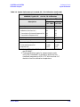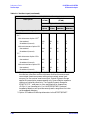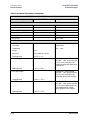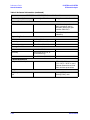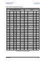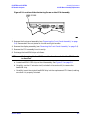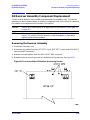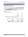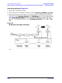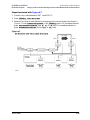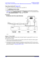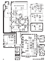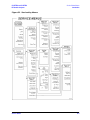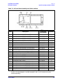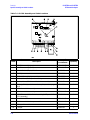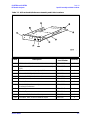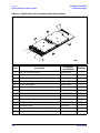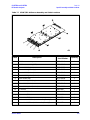
1
Service Guide Agilent Technologies 8712ET/ES and 8714ET/ES RF Network Analyzers Part No. 08714-90017 Printed in USA March 2000 Supersedes: October 1999 © Copyright 1998, 1999, 2000 Agilent Technologies Notice. This information contained in this document is subject to change without notice. Agilent Techologies makes no warranty of any kind with regard to this material, including but not limited to, the implied warranties of merchantability and fitness for a particular purpose. Agilent Techologies shall not be liable for errors contained herein or for incidental or consequential damages in connection with the furnishing, performance, or use of this material. Windows is a registered trademark of Microsoft Corporation. TORX is a registered trademark of TORX Products, division of Camcar/Textron Corporation. Certification Agilent Techologies certifies that this product met its published specifications at the time of shipment from the factory. Agilent Techologies further certifies that its calibration measurements are tractable to the United States National Institute of Standards and Technology, to the extent allowed by the Institute’s calibration facility, and to the calibration facilities of other International Standards Organization members. Regulatory Information The regulatory information is in the User’s Guide supplied with the analyzer. Safety, Warranty, and Assistance Refer to Chapter 9 for information on safety, warranty, and assistance. How to Use This Guide This guide uses the following conventions: FRONT PANEL KEY : This represents a key physically located on the instrument. Softkey : This indicates a “softkey,” a key whose label is determined by the instruments firmware, and is displayed on the right side of the instrument’s screen next to the eight unlabeled keys. Screen Text: This indicates text displayed on the instrument’s screen. This guide contains servicing information for the following instruments: • 8712ET • 8712ES • 8714ET • 8714ES iii 8712ET/ES and 8714ET/ES Network Analyzer Documentation Map The CDROM provides the contents of all of the documents listed below. The User’s Guide shows how to make measurements, explains commonly-used features, and tells you how to get the most performance from the analyzer. The LAN Interface User’s Guide Supplement shows how to use a local area network (LAN) for programming and remote operation of the analyzer. The Automating Measurements User’s Guide Supplement provides information on how to configure and control test systems for automation of test processes. The Programmer’s Guide provides programming information including GPIB and SCPI command references, as well as short programming examples. The Example Programs Guide provides a tutorial introduction using BASIC programming examples to demonstrate the remote operation of the analyzer. The Service Guide provides the information needed to adjust, troubleshoot, repair, and verify analyzer conformance to published specifications. The HP Instrument BASIC User’s Handbook describes programming and interfacing techniques using HP Instrument BASIC, and includes a language reference. iv The HP Instrument BASIC User’s Handbook Supplement shows how to use HP Instrument BASIC to program the analyzer. The Option 100 Fault Location and Structural Return Loss Measurements User’s Guide Supplement provides theory and measurement examples for making fault location and SRL measurements. (Shipped only with Option 100 analyzers.) The CATV Quick Start Guide provides abbreviated instructions for testing the quality of coaxial cables. (Shipped only with Option 100 analyzers.) The Cellular Antenna Quick Start Guide provides abbreviated instructions for verifying the performance of cellular antenna systems. (Shipped only with Option 100 analyzers.) v Contents 1. Performance Checks Performing the Operator's Check . . . . . . . . . . . . . . . . . . . . . . . . . . . . . . . . . . . . . . . . . . . . . . .1-3 Equipment List . . . . . . . . . . . . . . . . . . . . . . . . . . . . . . . . . . . . . . . . . . . . . . . . . . . . . . . . . . . .1-3 Make a Transmission (or S21 and S12) Measurement(s) . . . . . . . . . . . . . . . . . . . . . . . . . . .1-4 Make a Broadband Power Measurement. . . . . . . . . . . . . . . . . . . . . . . . . . . . . . . . . . . . . . . .1-6 Make a Reflection (or S11 and S22) Measurement with a Cable . . . . . . . . . . . . . . . . . . . . .1-7 Make a Reflection (or S11 and S22) Measurement with a Load . . . . . . . . . . . . . . . . . . . . .1-8 If the Analyzer Fails the Operator’s Check . . . . . . . . . . . . . . . . . . . . . . . . . . . . . . . . . . . . . .1-9 Performance Test Software . . . . . . . . . . . . . . . . . . . . . . . . . . . . . . . . . . . . . . . . . . . . . . . . . . .1-10 Required Software and Controller . . . . . . . . . . . . . . . . . . . . . . . . . . . . . . . . . . . . . . . . . . . .1-10 Estimated Time . . . . . . . . . . . . . . . . . . . . . . . . . . . . . . . . . . . . . . . . . . . . . . . . . . . . . . . . . . .1-11 Equipment . . . . . . . . . . . . . . . . . . . . . . . . . . . . . . . . . . . . . . . . . . . . . . . . . . . . . . . . . . . . . . .1-12 File Structure . . . . . . . . . . . . . . . . . . . . . . . . . . . . . . . . . . . . . . . . . . . . . . . . . . . . . . . . . . . .1-13 Configuration File . . . . . . . . . . . . . . . . . . . . . . . . . . . . . . . . . . . . . . . . . . . . . . . . . . . . . . . . .1-14 Getting Started . . . . . . . . . . . . . . . . . . . . . . . . . . . . . . . . . . . . . . . . . . . . . . . . . . . . . . . . . . .1-15 Performance Test Software Installation . . . . . . . . . . . . . . . . . . . . . . . . . . . . . . . . . . . . . . .1-15 Using the Program . . . . . . . . . . . . . . . . . . . . . . . . . . . . . . . . . . . . . . . . . . . . . . . . . . . . . . . .1-19 Performance Test Notes and Descriptions . . . . . . . . . . . . . . . . . . . . . . . . . . . . . . . . . . . . . .1-23 Specifications . . . . . . . . . . . . . . . . . . . . . . . . . . . . . . . . . . . . . . . . . . . . . . . . . . . . . . . . . . . . . .1-36 Definitions . . . . . . . . . . . . . . . . . . . . . . . . . . . . . . . . . . . . . . . . . . . . . . . . . . . . . . . . . . . . . . .1-36 System Performance. . . . . . . . . . . . . . . . . . . . . . . . . . . . . . . . . . . . . . . . . . . . . . . . . . . . . . . . .1-37 Test Port Output. . . . . . . . . . . . . . . . . . . . . . . . . . . . . . . . . . . . . . . . . . . . . . . . . . . . . . . . . . . .1-57 Test Port Input . . . . . . . . . . . . . . . . . . . . . . . . . . . . . . . . . . . . . . . . . . . . . . . . . . . . . . . . . . . . .1-63 General Information. . . . . . . . . . . . . . . . . . . . . . . . . . . . . . . . . . . . . . . . . . . . . . . . . . . . . . . . .1-73 Features . . . . . . . . . . . . . . . . . . . . . . . . . . . . . . . . . . . . . . . . . . . . . . . . . . . . . . . . . . . . . . . . . .1-79 Measurement. . . . . . . . . . . . . . . . . . . . . . . . . . . . . . . . . . . . . . . . . . . . . . . . . . . . . . . . . . . . .1-79 Storage . . . . . . . . . . . . . . . . . . . . . . . . . . . . . . . . . . . . . . . . . . . . . . . . . . . . . . . . . . . . . . . . . .1-80 Data Hardcopy . . . . . . . . . . . . . . . . . . . . . . . . . . . . . . . . . . . . . . . . . . . . . . . . . . . . . . . . . . .1-81 Automation . . . . . . . . . . . . . . . . . . . . . . . . . . . . . . . . . . . . . . . . . . . . . . . . . . . . . . . . . . . . . .1-81 Measurement Calibration. . . . . . . . . . . . . . . . . . . . . . . . . . . . . . . . . . . . . . . . . . . . . . . . . . .1-82 Options. . . . . . . . . . . . . . . . . . . . . . . . . . . . . . . . . . . . . . . . . . . . . . . . . . . . . . . . . . . . . . . . . .1-85 2. Adjustments Introduction . . . . . . . . . . . . . . . . . . . . . . . . . . . . . . . . . . . . . . . . . . . . . . . . . . . . . . . . . . . . . . . .2-2 Required Equipment . . . . . . . . . . . . . . . . . . . . . . . . . . . . . . . . . . . . . . . . . . . . . . . . . . . . . . . .2-3 Correction Constants (CCs) Storage . . . . . . . . . . . . . . . . . . . . . . . . . . . . . . . . . . . . . . . . . . . . .2-4 Frequency Accuracy Adjustment. . . . . . . . . . . . . . . . . . . . . . . . . . . . . . . . . . . . . . . . . . . . . . . .2-5 Set Serial Number, Adjustment #100 . . . . . . . . . . . . . . . . . . . . . . . . . . . . . . . . . . . . . . . . . . . .2-7 LO Power Correction, Adjustment #101 . . . . . . . . . . . . . . . . . . . . . . . . . . . . . . . . . . . . . . . . . .2-9 Switched Gain Correction, Adjustment #102 . . . . . . . . . . . . . . . . . . . . . . . . . . . . . . . . . . . . .2-10 External Detector Gain Correction, Adjustment #103 . . . . . . . . . . . . . . . . . . . . . . . . . . . . . .2-12 Auxiliary Input Correction, Adjustment #111 . . . . . . . . . . . . . . . . . . . . . . . . . . . . . . . . . . . .2-14 Source Power Correction, Adjustment #104 . . . . . . . . . . . . . . . . . . . . . . . . . . . . . . . . . . . . . .2-15 B Amplitude Correction, Adjustment #105. . . . . . . . . . . . . . . . . . . . . . . . . . . . . . . . . . . . . . .2-18 Reflection (One-Port) Correction, Adjustment #107 . . . . . . . . . . . . . . . . . . . . . . . . . . . . . . . .2-19 Transmission Correction, Adjustment #106 . . . . . . . . . . . . . . . . . . . . . . . . . . . . . . . . . . . . . .2-20 B* Amplitude Correction, Adjustment #110. . . . . . . . . . . . . . . . . . . . . . . . . . . . . . . . . . . . . .2-21 R* Amplitude Correction, Adjustment #108. . . . . . . . . . . . . . . . . . . . . . . . . . . . . . . . . . . . . .2-23 R* Frequency Response Correction, Adjustment #109 . . . . . . . . . . . . . . . . . . . . . . . . . . . . .2-25 Contents-vii Contents 3. Assembly Replacement Introduction . . . . . . . . . . . . . . . . . . . . . . . . . . . . . . . . . . . . . . . . . . . . . . . . . . . . . . . . . . . . . . . . 3-2 Required Tools . . . . . . . . . . . . . . . . . . . . . . . . . . . . . . . . . . . . . . . . . . . . . . . . . . . . . . . . . . . . 3-2 Assembly Removal/Replacement Procedures. . . . . . . . . . . . . . . . . . . . . . . . . . . . . . . . . . . . . . 3-3 A1 Front Panel Assembly Replacement . . . . . . . . . . . . . . . . . . . . . . . . . . . . . . . . . . . . . . . . . . 3-4 Removing the Front Panel Assembly . . . . . . . . . . . . . . . . . . . . . . . . . . . . . . . . . . . . . . . . . . 3-4 Installing the Front Panel Assembly. . . . . . . . . . . . . . . . . . . . . . . . . . . . . . . . . . . . . . . . . . . 3-5 A2 CPU Board Assembly Replacement . . . . . . . . . . . . . . . . . . . . . . . . . . . . . . . . . . . . . . . . . . 3-6 Removing the CPU Board Assembly . . . . . . . . . . . . . . . . . . . . . . . . . . . . . . . . . . . . . . . . . . . 3-6 Installing the CPU Board Assembly . . . . . . . . . . . . . . . . . . . . . . . . . . . . . . . . . . . . . . . . . . . 3-9 A3 Fractional-N/Reference Assembly Replacement . . . . . . . . . . . . . . . . . . . . . . . . . . . . . . . 3-10 Removing the Fractional-N/Reference Assembly . . . . . . . . . . . . . . . . . . . . . . . . . . . . . . . . 3-10 Installing the Fractional-N/Reference Assembly . . . . . . . . . . . . . . . . . . . . . . . . . . . . . . . . 3-10 A4 Source Assembly Replacement . . . . . . . . . . . . . . . . . . . . . . . . . . . . . . . . . . . . . . . . . . . . . 3-11 Removing the Source Assembly. . . . . . . . . . . . . . . . . . . . . . . . . . . . . . . . . . . . . . . . . . . . . . 3-11 Installing the Source Assembly . . . . . . . . . . . . . . . . . . . . . . . . . . . . . . . . . . . . . . . . . . . . . . 3-12 A5 Receiver Assembly Component Replacement. . . . . . . . . . . . . . . . . . . . . . . . . . . . . . . . . . 3-13 Removing the Receiver Assembly . . . . . . . . . . . . . . . . . . . . . . . . . . . . . . . . . . . . . . . . . . . . 3-13 Installing the Receiver Assembly . . . . . . . . . . . . . . . . . . . . . . . . . . . . . . . . . . . . . . . . . . . . 3-18 A6 Power Supply Assembly Replacement . . . . . . . . . . . . . . . . . . . . . . . . . . . . . . . . . . . . . . . 3-19 Removing the Power Supply Assembly . . . . . . . . . . . . . . . . . . . . . . . . . . . . . . . . . . . . . . . . 3-19 Installing the Power Supply Assembly . . . . . . . . . . . . . . . . . . . . . . . . . . . . . . . . . . . . . . . . 3-19 A7 Display Assembly Replacement . . . . . . . . . . . . . . . . . . . . . . . . . . . . . . . . . . . . . . . . . . . . 3-20 Removing the Display Assembly . . . . . . . . . . . . . . . . . . . . . . . . . . . . . . . . . . . . . . . . . . . . . 3-20 A8 Internal Disk Drive Assembly Replacement . . . . . . . . . . . . . . . . . . . . . . . . . . . . . . . . . . 3-22 Removing the 3.5" Disk Drive Assembly. . . . . . . . . . . . . . . . . . . . . . . . . . . . . . . . . . . . . . . 3-22 Installing the 3.5" Disk Drive Assembly . . . . . . . . . . . . . . . . . . . . . . . . . . . . . . . . . . . . . . . 3-22 Post Repair Procedures . . . . . . . . . . . . . . . . . . . . . . . . . . . . . . . . . . . . . . . . . . . . . . . . . . . . . . 3-23 How to Order Parts . . . . . . . . . . . . . . . . . . . . . . . . . . . . . . . . . . . . . . . . . . . . . . . . . . . . . . . . . 3-24 Save Money by Ordering R-E (Rebuilt-Exchange) Assemblies . . . . . . . . . . . . . . . . . . . . . 3-24 4.Troubleshooting and Block Diagrams Introduction . . . . . . . . . . . . . . . . . . . . . . . . . . . . . . . . . . . . . . . . . . . . . . . . . . . . . . . . . . . . . . . . 4-2 General Notes . . . . . . . . . . . . . . . . . . . . . . . . . . . . . . . . . . . . . . . . . . . . . . . . . . . . . . . . . . . . . 4-2 Service Kit . . . . . . . . . . . . . . . . . . . . . . . . . . . . . . . . . . . . . . . . . . . . . . . . . . . . . . . . . . . . . . . 4-3 Initial Observations — Normal Power-up Sequence . . . . . . . . . . . . . . . . . . . . . . . . . . . . . . 4-5 Operator's Check . . . . . . . . . . . . . . . . . . . . . . . . . . . . . . . . . . . . . . . . . . . . . . . . . . . . . . . . . . 4-6 Category 1 Failures: Dead or No Display . . . . . . . . . . . . . . . . . . . . . . . . . . . . . . . . . . . . . . . . . 4-7 Troubleshooting the Power Supply Assembly (A6). . . . . . . . . . . . . . . . . . . . . . . . . . . . . . . . 4-7 Troubleshooting Digital Group Problems . . . . . . . . . . . . . . . . . . . . . . . . . . . . . . . . . . . . . . 4-10 Error Occurs During DSP Initialization or Calculating Coefficients . . . . . . . . . . . . . . . . 4-16 Front Panel Problems. . . . . . . . . . . . . . . . . . . . . . . . . . . . . . . . . . . . . . . . . . . . . . . . . . . . . . 4-17 Other Power-Up Problems . . . . . . . . . . . . . . . . . . . . . . . . . . . . . . . . . . . . . . . . . . . . . . . . . . 4-17 Other Error Messages . . . . . . . . . . . . . . . . . . . . . . . . . . . . . . . . . . . . . . . . . . . . . . . . . . . . . 4-17 Category 2 Failures: No Error Messages but One or More Measurements Are Nonfunctional . . . . . . . . . . . . . . . . . . . . . . . . . . . . . . . . . . . . . . . . . . . . . . . . . . . . . . . . . . . . . 4-18 Category 2 (ET Analyzer Troubleshooting) . . . . . . . . . . . . . . . . . . . . . . . . . . . . . . . . . . . . 4-18 Category 2 (ES Analyzer Troubleshooting). . . . . . . . . . . . . . . . . . . . . . . . . . . . . . . . . . . . . 4-23 General Troubleshooting for Both ET and ES Models . . . . . . . . . . . . . . . . . . . . . . . . . . . . 4-30 Contents-viii Contents Category 3 Failures: Inaccurate (but reasonably functional) Measurements. . . . . . . . . . . .4-33 Troubleshooting Inaccurate Data. . . . . . . . . . . . . . . . . . . . . . . . . . . . . . . . . . . . . . . . . . . . .4-33 RF Power Problems. . . . . . . . . . . . . . . . . . . . . . . . . . . . . . . . . . . . . . . . . . . . . . . . . . . . . . . .4-37 Category 4 Failures: Peripheral Device Problems . . . . . . . . . . . . . . . . . . . . . . . . . . . . . . . . .4-38 DIN Keyboard . . . . . . . . . . . . . . . . . . . . . . . . . . . . . . . . . . . . . . . . . . . . . . . . . . . . . . . . . . . .4-38 RS-232 Printers and Plotters . . . . . . . . . . . . . . . . . . . . . . . . . . . . . . . . . . . . . . . . . . . . . . . .4-38 Floppy Disk Drive Maintenance. . . . . . . . . . . . . . . . . . . . . . . . . . . . . . . . . . . . . . . . . . . . . .4-38 Centronics (Parallel) Printers and Plotters . . . . . . . . . . . . . . . . . . . . . . . . . . . . . . . . . . . . .4-39 GPIB Systems . . . . . . . . . . . . . . . . . . . . . . . . . . . . . . . . . . . . . . . . . . . . . . . . . . . . . . . . . . . .4-39 LAN Troubleshooting . . . . . . . . . . . . . . . . . . . . . . . . . . . . . . . . . . . . . . . . . . . . . . . . . . . . . .4-40 5. Service Related Menus Introduction . . . . . . . . . . . . . . . . . . . . . . . . . . . . . . . . . . . . . . . . . . . . . . . . . . . . . . . . . . . . . . . .5-2 Tests and Adjustments Menu . . . . . . . . . . . . . . . . . . . . . . . . . . . . . . . . . . . . . . . . . . . . . . . . . .5-4 Select Self-Test Menu. . . . . . . . . . . . . . . . . . . . . . . . . . . . . . . . . . . . . . . . . . . . . . . . . . . . . . . . .5-5 Select Adjustment Menu . . . . . . . . . . . . . . . . . . . . . . . . . . . . . . . . . . . . . . . . . . . . . . . . . . . . . .5-8 Instrument Info . . . . . . . . . . . . . . . . . . . . . . . . . . . . . . . . . . . . . . . . . . . . . . . . . . . . . . . . . . . .5-10 Update Corr Const Menu. . . . . . . . . . . . . . . . . . . . . . . . . . . . . . . . . . . . . . . . . . . . . . . . . . . . .5-11 Service Utilities Menu 1 . . . . . . . . . . . . . . . . . . . . . . . . . . . . . . . . . . . . . . . . . . . . . . . . . . . . .5-12 Meas Cal Options Menu. . . . . . . . . . . . . . . . . . . . . . . . . . . . . . . . . . . . . . . . . . . . . . . . . . . . . .5-15 Analog Bus Menu . . . . . . . . . . . . . . . . . . . . . . . . . . . . . . . . . . . . . . . . . . . . . . . . . . . . . . . . . . .5-16 Service Utilities Menu 2 . . . . . . . . . . . . . . . . . . . . . . . . . . . . . . . . . . . . . . . . . . . . . . . . . . . . .5-19 Service Utilities Menu 3 . . . . . . . . . . . . . . . . . . . . . . . . . . . . . . . . . . . . . . . . . . . . . . . . . . . . .5-20 View Array Master Menu /View Array Interpol Menu. . . . . . . . . . . . . . . . . . . . . . . . . . . . . .5-21 Miscellaneous Service Functions. . . . . . . . . . . . . . . . . . . . . . . . . . . . . . . . . . . . . . . . . . . . . . .5-22 Clearing Nonvolatile Memory (SRAM) . . . . . . . . . . . . . . . . . . . . . . . . . . . . . . . . . . . . . . . .5-22 GPIB Command Reference for Service . . . . . . . . . . . . . . . . . . . . . . . . . . . . . . . . . . . . . . . . . .5-23 Syntax Summary. . . . . . . . . . . . . . . . . . . . . . . . . . . . . . . . . . . . . . . . . . . . . . . . . . . . . . . . . .5-23 Softkey SCPI Commands . . . . . . . . . . . . . . . . . . . . . . . . . . . . . . . . . . . . . . . . . . . . . . . . . . .5-23 Alphabetical SCPI Command Summary . . . . . . . . . . . . . . . . . . . . . . . . . . . . . . . . . . . . . . .5-24 6. Theory of Operation Introduction . . . . . . . . . . . . . . . . . . . . . . . . . . . . . . . . . . . . . . . . . . . . . . . . . . . . . . . . . . . . . . . .6-2 System Theory . . . . . . . . . . . . . . . . . . . . . . . . . . . . . . . . . . . . . . . . . . . . . . . . . . . . . . . . . . . . . .6-3 The Analyzer Functional Groups . . . . . . . . . . . . . . . . . . . . . . . . . . . . . . . . . . . . . . . . . . . . . .6-3 Power Supply (A6). . . . . . . . . . . . . . . . . . . . . . . . . . . . . . . . . . . . . . . . . . . . . . . . . . . . . . . . . .6-6 Digital Control Group . . . . . . . . . . . . . . . . . . . . . . . . . . . . . . . . . . . . . . . . . . . . . . . . . . . . . . .6-6 Source Group . . . . . . . . . . . . . . . . . . . . . . . . . . . . . . . . . . . . . . . . . . . . . . . . . . . . . . . . . . . . . .6-8 Receiver Assembly (A5) . . . . . . . . . . . . . . . . . . . . . . . . . . . . . . . . . . . . . . . . . . . . . . . . . . . .6-12 7. Parts List Analyzer Hardware . . . . . . . . . . . . . . . . . . . . . . . . . . . . . . . . . . . . . . . . . . . . . . . . . . . . . . . . . .7-2 Specific Assembly and Cable Locations. . . . . . . . . . . . . . . . . . . . . . . . . . . . . . . . . . . . . . . . . . .7-3 8. Correction Constants and Firmware Storing and Recalling Correction Constants (CC) . . . . . . . . . . . . . . . . . . . . . . . . . . . . . . . . . .8-2 Storing Correction Constants to Disk . . . . . . . . . . . . . . . . . . . . . . . . . . . . . . . . . . . . . . . . . .8-3 Loading Correction Constants from Disk . . . . . . . . . . . . . . . . . . . . . . . . . . . . . . . . . . . . . . .8-3 Contents-ix Contents Storing Correction Constants to EPROM . . . . . . . . . . . . . . . . . . . . . . . . . . . . . . . . . . . . . . . 8-4 Installing Correction Constants from Disk. . . . . . . . . . . . . . . . . . . . . . . . . . . . . . . . . . . . . . 8-4 In Case of Difficulties . . . . . . . . . . . . . . . . . . . . . . . . . . . . . . . . . . . . . . . . . . . . . . . . . . . . . . . 8-4 Upgrading or Re-Installing Firmware . . . . . . . . . . . . . . . . . . . . . . . . . . . . . . . . . . . . . . . . . . . 8-5 How to Upgrade or Re-Install the Firmware . . . . . . . . . . . . . . . . . . . . . . . . . . . . . . . . . . . . 8-5 9. Safety, Warranty, and Assistance Safety Symbols. . . . . . . . . . . . . . . . . . . . . . . . . . . . . . . . . . . . . . . . . . . . . . . . . . . . . . . . . . . . . . 9-2 General Safety Considerations . . . . . . . . . . . . . . . . . . . . . . . . . . . . . . . . . . . . . . . . . . . . . . . . . 9-3 Safety Earth Ground . . . . . . . . . . . . . . . . . . . . . . . . . . . . . . . . . . . . . . . . . . . . . . . . . . . . . . . 9-3 Servicing . . . . . . . . . . . . . . . . . . . . . . . . . . . . . . . . . . . . . . . . . . . . . . . . . . . . . . . . . . . . . . . . . 9-3 Lithium Battery Disposal . . . . . . . . . . . . . . . . . . . . . . . . . . . . . . . . . . . . . . . . . . . . . . . . . . . . . 9-4 Warranty . . . . . . . . . . . . . . . . . . . . . . . . . . . . . . . . . . . . . . . . . . . . . . . . . . . . . . . . . . . . . . . . . . 9-5 Limitation of Warranty . . . . . . . . . . . . . . . . . . . . . . . . . . . . . . . . . . . . . . . . . . . . . . . . . . . . . 9-5 Exclusive Remedies . . . . . . . . . . . . . . . . . . . . . . . . . . . . . . . . . . . . . . . . . . . . . . . . . . . . . . . . 9-5 Assistance . . . . . . . . . . . . . . . . . . . . . . . . . . . . . . . . . . . . . . . . . . . . . . . . . . . . . . . . . . . . . . . . . 9-6 Shipment for Service . . . . . . . . . . . . . . . . . . . . . . . . . . . . . . . . . . . . . . . . . . . . . . . . . . . . . . . . . 9-6 Contents-x 8712ET/ES and 8714ET/ES RF Network Analyzers 1 Performance Checks Service Guide 1-1 Performance Checks 8712ET/ES and 8714ET/ES RF Network Analyzers This chapter is divided into three parts: • “Performing the Operator's Check” on page 1-3 • “Performance Test Software” on page 1-10 • “Specifications” on page 1-36 The operator's check can be used as a quick 80% confidence test. The only equipment required for this check is a type-N cable and a good quality 50Ω type-N load (75Ω for Option 1EC analyzers). The performance tests will verify that the analyzer meets its published specifications with greater than a 95% confidence level. The performance tests require an external controller running HP BASIC and are completely automated. The specifications provide a complete definition of the warranted and non-warranted characteristics of the analyzer. 1-2 Service Guide 8712ET/ES and 8714ET/ES RF Network Analyzers Performance Checks Performing the Operator's Check Performing the Operator's Check The operator's check should be performed when you receive your instrument, and any time you wish to have confidence that the analyzer is working properly. The operator's check does not verify conformance to specifications, but should give you a high degree of confidence that the instrument is performing properly if it passes. The operator's check consists of making the following measurements with the cable that was supplied with your analyzer: 8712ET/8714ET 8712ES/8714ES transmission S21 and S12 broadband power broadband power reflection S11 and S22 reflection1 S11 and S221 1.with a 50Ω or 75Ω load, instead of the cable Equipment List To perform the operator's check, you will need the following: • A known good cable such as the one that was supplied with your analyzer. The cable you use should have ≤0.5 dB of insertion loss up to 1.3 GHz, and ≤0.75 dB of insertion loss from 1.3 to 3.0 GHz. • A known good load (>40 dB return loss) that matches the test port impedance of your analyzer such as one from calibration kit HP/Agilent 85032B/E (50Ω) or HP/Agilent 85036B/E (75Ω). NOTE Service Guide The illustrations depicting the analyzer’s display in this section were made using an 8714ET. Other models’ displays will have minor differences in annotation. 1-3 Performance Checks Performing the Operator's Check 8712ET/ES and 8714ET/ES RF Network Analyzers Make a Transmission (or S21 and S12) Measurement(s) 1. Connect the equipment as shown in Figure 1-1. Use a known good cable such as the one that was supplied with your analyzer. The quality of the cable will affect these measurements; make sure you use a cable with the characteristics described in “Equipment List” on page 1-3. NOTE Figure 1-1 Equipment Setup for Performing the Operator’s Check 2. Press PRESET SCALE 3. Press POWER 0 4. Press CAL .1 Enter . dBm . Default Response . 5. Verify that the data trace falls within ±0.5 dB of 0 dB. See Figure 1-2 for a typical 8714 result. The 8712 should look similar, but will end at 1300 MHz. 1-4 Service Guide 8712ET/ES and 8714ET/ES RF Network Analyzers Figure 1-2 Performance Checks Performing the Operator's Check Verify Transmission (or S21 and S12) Measurement Perform the following steps on ES model analyzers only. 6. Press MEAS 1 7. Press CAL S12 Rev Trans . Default Response . 8. Verify again that the data trace falls within ±0.5 dB of 0 dB. See Figure 1-2. Service Guide 1-5 Performance Checks Performing the Operator's Check 8712ET/ES and 8714ET/ES RF Network Analyzers Make a Broadband Power Measurement 1. Leave the cable connected to the analyzer as shown in Figure 1-1. NOTE The quality of the cable will affect these measurements; make sure you use a cable with the characteristics described in “Equipment List” on page 1-3. 2. Press MEAS 1 . 3. If Power is not displayed, press More . 4. Press Power 5. Press POWER FREQ 0 Start 10 MHz SCALE 1 Enter . dBm . 6. Verify that the data trace is within ±2 dB of 0 dBm. See Figure 1-3 for a typical 8714 result. The 8712 should look similar, but will end at 1300 MHz. Figure 1-3 1-6 Verify Broadband Power Measurement Service Guide 8712ET/ES and 8714ET/ES RF Network Analyzers Performance Checks Performing the Operator's Check Make a Reflection (or S11 and S22) Measurement with a Cable 1. Leave the cable connected to the analyzer as shown in Figure 1-1. NOTE The quality of the cable will affect these measurements; make sure you use a cable with the characteristics described in “Equipment List” on page 1-3. 2. Press PRESET MEAS 1 . 3. For ES models, press S11 Refl Port1 . For ET models, press Reflection . 4. Press SCALE 5. Press POWER 6. Press CAL 10 Enter . 0 dBm . Default 1-Port . 7. Verify that the data trace falls completely below −16 dB. See Figure 1-4 for a typical 8714 result. The 8712 should look similar, but will end at 1300 MHz. Figure 1-4 Verify Reflection (or S11 and S22) Measurement Perform the following steps on ES model analyzers only. 8. Press MEAS 1 9. Press CAL S22 Refl Port2 . Default 1-Port . 10.Verify again that the data trace falls completely below −16 dB. See Figure 1-4. Service Guide 1-7 Performance Checks Performing the Operator's Check 8712ET/ES and 8714ET/ES RF Network Analyzers Make a Reflection (or S11 and S22) Measurement with a Load 1. Disconnect the cable and connect a known good load to the RF OUT/PORT 1 test port as shown in Figure 1-5. Figure 1-5 Connect the Load 2. For ES models, press MEAS 1 S11 Refl Port1 . 3. Verify that the data trace falls below −30 dB. If the data trace is off the screen, press SCALE Reference Level and the key until the trace moves up onto the screen. Perform the remaining steps on ES model analyzers only. 4. Disconnect the load from PORT 1 and connect it to PORT 2 as shown in Figure 1-6. Figure 1-6 5. Press MEAS 1 Connect the Load to Port 2 (ES Models only) S22 Refl Port2 . 6. Verify that the data trace falls below −30 dB. If the data trace is off the screen, press key until the trace moves up onto the screen. SCALE Reference Level and the 1-8 Service Guide 8712ET/ES and 8714ET/ES RF Network Analyzers Performance Checks Performing the Operator's Check This concludes the operator's check. However, further confidence can be obtained by performing the following: • Measure a known filter to verify that its measured response is the same as is expected. (A 175 MHz filter is supplied with the analyzer.) Verify both the frequency accuracy and noise floor. • Check broadband response with the filter using conversion-loss mode (same as B*/R*). • If the analyzer's frequency accuracy is critical for your application, verify a CW frequency using a frequency counter. Verify to ±.005% accuracy (for example, ± 2500 Hz at 500 MHz). Ensure that the analyzer is placed in trigger-hold mode (press MENU Trigger Hold ) to measure frequencies. If the Analyzer Fails the Operator’s Check First, repeat the operator's check using a different cable and load to eliminate these as a possible cause of failure. Second, if the floppy disk from the factory labeled “Correction Constants” is available, reload the “Correction Constants” (CCs) per Chapter 8, “Correction Constants and Firmware.” (The floppy disk was shipped with the instrument from the factory.) Then repeat the Operator’s Check. If your analyzer does not meet the criteria in the operator's check, your analyzer may need adjustment or servicing. Contact any Agilent Technologies sales or service office for assistance. Refer to Table 9-1 on page 9-7 for the nearest office. Before shipping your analyzer, fill out and attach the blue repair tag, located at the back of this manual. Service Guide 1-9 Performance Checks Performance Test Software 8712ET/ES and 8714ET/ES RF Network Analyzers Performance Test Software The performance test software provides automated tests for verifying that the analyzer meets its published specifications with greater than a 95% confidence level. The performance test software must be run on an external controller running HP BASIC (the analyzer’s internal IBASIC cannot be used). The performance tests can be considered a check of the overall calibration of the instrument. Unlike the adjustments described in Chapter 2, the performance test software only checks the performance of the analyzer. No changes are made to the calibration constants stored in the instrument. When a performance test fails, usually one or more adjustments should be performed to attempt to improve the performance before repairing or replacing hardware. Results of the automated performance tests can be printed out at any time. They include all specifications, limits, and uncertainties. Although no manual tests are provided, each of the automated tests is described in enough detail to allow a knowledgeable technician to perform all needed tests in an accurate manner. See “Performance Test Notes and Descriptions” on page 1-23. The printed test results list uncertainties for each measurement. These uncertainties are for reference only, and are not taken into consideration when making pass/fail determinations. The listed uncertainties do not depend on the level of the measured signal; they assume a signal at the specified level. Generally, uncertainties assume published specifications for all instruments and devices. For the 110 dB step attenuator and the 20 dB fixed attenuator, device-specific calibration data is required. Performance test record cards are not provided; the printed results of the automated performance testing serve as the test record for this product. See “ PRINT RESULTS ” in “Using the Program” on page 1-19 for details on pass/fail indications for individual tests. When a test report contains no “FAIL” indicators, an analyzer is considered to have passed the performance tests. Many instrument users require a periodic, documented check of instrument performance. This is usually referred to as a “periodic calibration.” Successful completion of the performance tests (no “FAIL” indicators) should suffice for the requirements of a periodic calibration. Do not confuse the term “periodic calibration” with the terms “user calibration” or “default calibration” which both refer to measurement calibrations utilized by operators when measuring devices with the analyzer. Required Software and Controller The performance test software is written for an HP 9000 Series 200, 300, or 700 workstation (or equivalent), running HP BASIC 5.1 or greater. There is also a version available to run on a PC under HP BASIC for Windows with a GPIB interface card. Operation is essentially identical to that described for an HP workstation computer. 1-10 Service Guide 8712ET/ES and 8714ET/ES RF Network Analyzers NOTE Performance Checks Performance Test Software To order the performance test software, contact the nearest Agilent Technologies sales or service office listed in Table 9-1 on page 9-7. The workstation version is HP part number 08714-10001 (LIF format). The PC version is HP part number 08714-10002 (DOS format), and requires HP BASIC for Windows (HP model number E2060B), and a GPIB interface card. The performance test software automates all the performance verification tests for the 8712ET/ES and the 8714ET/ES. It will test all option combinations, including both 50Ω and 75Ω versions. NOTE This program cannot be used to test an HP/Agilent 8711A, any HP/Agilent 871xB, or any HP/Agilent 871xC. To test an HP/Agilent 8711A, order HP part number 08711-10011. To test an HP/Agilent 871xB, order HP part number 08712-10011. Both of these programs are in LIF format only. To test an HP/Agilent 871xC, order HP part number 08712-10017 (LIF format) or 08712-10018 (DOS format). NOTE All the data files and configuration files used in this program are compatible with the previous 871xB and 871xC versions of this program. It is not necessary to regenerate or modify any of these files. If you are adding this program to the same directory as the 871xB/C software, only the main program file (CAL871XE) need be transferred. The performance test software is provided on a single disk. You can run the program directly from the disk, although it is recommended that you run it from your system's hard disk for best performance. Generally, the program can be stopped, reset and re-run with little or no loss of data. The LIF version program will operate on a LIF-based system, or an SRM/HFS environment. The DOS version is limited to DOS environments. Operation is a simple menu driven system with some softkey selections. For ease of use, the Return / Enter / Execute keys on your computer’s keyboard can always be used as softkey #1—the most frequently used key. NOTE All necessary instructions and test setup diagrams are contained within the program. A disk file is generated for each analyzer, and the results of each test are stored in that file. This file is updated after each test so that results will not be accidentally lost. A printout can be obtained for any previously tested analyzer. Estimated Time Before running the performance tests, turn on the analyzer and allow it to warm up for one hour. Performance test times are kept to a minimum, allowing analyzers to be fully tested within one to two hours after the initial warmup. Service Guide 1-11 Performance Checks Performance Test Software 8712ET/ES and 8714ET/ES RF Network Analyzers Equipment In addition to a computer, printer, RF cables, BNC cables, GPIB cables, and adapters, Table 1-1 lists the equipment that is required to test and adjust the analyzer. Table 1-1 Required Equipment for Performance Tests Description HP/Agilent Model # 50Ω STD 75Ω Notes Function generator 8116A or 33120A ✓ ✓ No substitute. (The 8116A is preferred.) Power meter 437B, 438A E4418A or E4419A ✓ ✓ Do not use an 436A. Power sensor, 50Ω 8482A ✓ ✓ Power sensor, 75Ω 8483A — ✓ ✓ — 0011 Cal kit type-N 50Ω 85032B Opt Cal kit type-N 75Ω 85036B — ✓ External 110 dB step attenuator 8496A/G ✓ ✓ Attenuator/switch driver 11713A ✓ ✓ Needed only if using an 8496G programmable 110 dB step attenuator. Spectrum analyzer 8560 series, 8566B ✓ ✓ Others may be substituted.2 20 dB attenuator 50Ω 8491A/B/C Opt 020 ✓ — 0955-0768 — ✓ 6 dB attenuator 50Ω 8491A/B/C Opt 006 ✓ — 3 dB attenuator 50Ω 8491A/B/C Opt 003 ✓ — 3 dB attenuator 75Ω 0955-0765 — ✓ Power splitter, 50Ω 0955-0751,11667A ✓ — Power splitter, 75Ω 0955-0752 — ✓ Minimum loss pad (quantity: 2) 11852B — ✓ Precision cable 50Ω 8120-8862 or 8120-6469 ✓ — Precision cable 75Ω 8120-8898 or 8120-6468 — ✓ 20 dB attenuator 75Ω3 1. An 85032B Option 001 is a subset of the standard 85032B. This option eliminates four 7-mm adapters that are not needed, resulting in a significant cost savings. 2. The spectrum analyzer used must be compatible with the 8566B, both in the GPIB commands for the basic remote control functions and in frequency accuracy. Any of the 856x series is acceptable, the 8560E is the least expensive. The 859x series is not acceptable because of the marginal frequency accuracy. 3. The 75Ω 20 dB attenuator can be substituted with two minimum loss pads and a 50Ω 10 dB attenuator. NOTE: a set of 75Ω attenuators (3,6,10,20 dB) is available as 86213A. 1-12 Service Guide 8712ET/ES and 8714ET/ES RF Network Analyzers Performance Checks Performance Test Software File Structure The program disk contains several different files in addition to the main program file. The following list describes the files found on the performance test software disk. CAL871XE This is the main program file. Cfg_xxxx This is the configuration file. The variable xxxx represents any user-defined name or Dflt (default). This file contains all the configuration set-ups for the program such as: • file directories and paths • test equipment serial numbers • GPIB addresses • types of test equipment • other optional choices If more than one configuration file exists on the disk, the program will prompt you to select a specific configuration file to load. If none exists, the program will create a default file. P1D_xxxx The cal factor file for the HP/Agilent 8481D sensor. The variable xxxx represents the last four digits of the HP/Agilent 8481D or HP/Agilent 8484A sensor's serial number. P2A_xxxx The cal factor file for the HP/Agilent 8482A sensor. The variable xxxx represents the last four digits of the 8482A sensor's serial number. P3A_xxxx The cal factor file for the HP/Agilent 8483A sensor. The variable xxxx represents the last four digits of the 8483A sensor's serial number. Stp_xxxx The actual attenuation values for the external 110 dB step attenuator. The variable xxxx represents the last four digits in the attenuator's serial number. Attenuator values are measured at 30 MHz on an accurate system (such as an HP/Agilent 8902A Option 050). Pd5_xxxx The actual value of the 20 dB 50Ω attenuator as measured by an accurate system. Values are attenuation versus frequency. The variable xxxx represents the last four digits in the attenuator's serial number. Pd7_xxxx The actual value of the 20 dB 75Ω attenuator as measured by an accurate system. Values are attenuation versus frequency. The variable xxxx represents the last four digits in the attenuator's serial number. dxxExxxx The data file that holds the analyzer's test results. The variable xxxx represents the last four digits in the analyzer's serial number. The file “d2TExxxx” holds data for an 8712ET, “d4SExxxx” for an 8714ES. CurEDUTx The data file that holds the test results of the most recently tested analyzer regardless of model or serial number. The variable x can represent any character 0 to 9. Service Guide 1-13 Performance Checks Performance Test Software INSTALL NOTE 8712ET/ES and 8714ET/ES RF Network Analyzers This program is not necessary but can help speed the installation of the LIF version program. It automatically copies the required files into the desired location. Several data files are present on the disk with the “xxxx” suffix. These are default files that allow operation of the program without correction factors. The values in these file are nominal values. For example: 100 percent for all sensor cal factors; 20 dB for the 20 dB attenuators; 10.00, 20.00, 30…dB for the external step attenuator, and so on. This is provided as a convenience only to demonstrate or learn about the program. The default configuration file will access these files if no user-defined serial number is specified. A warning message will be displayed if the program is using these default files. Configuration File The configuration (config) file is the file that customizes this program for your usage. It contains specific information for your setup. Some of the items contained in this file include: • the GPIB addresses of all the test equipment • the GPIB address of the analyzer under test • the model numbers of the test equipment • the serial numbers of sensors, fixed attenuators, and the external 110 dB step attenuator • the disk drive locations (path and directories) • other items specific to your setup Ideally, only one configuration file should exist on the program disk so that the program will automatically load only that file. However, it is possible to have several configuration files stored on the same disk. In this case, the program will list all of the available files and prompt you to select one. This is useful if more than one setup is commonly used or if one performance test software disk serves several workstations. 1-14 Service Guide 8712ET/ES and 8714ET/ES RF Network Analyzers Performance Checks Performance Test Software Getting Started CAUTION Make a copy of the performance test software disk for day-to-day use. The master copy should remain stored in a safe place. This will decrease the likelihood of damage to the master disk. NOTE The DOS version, which is used in conjunction with HP BASIC for Windows, requires the proper setup of the GPIB interface card and drivers. This document assumes that users are familiar with HP BASIC for Windows, that it is running, and that it has been properly installed and configured. First, find all serial numbers of the calibration devices required, such as external step attenuators, sensors, and fixed attenuators for both 50Ω and 75Ω devices (if applicable). Verify the GPIB addresses you will be using, as well as the mass storage directories and locations. If you plan to operate this program only from the supplied floppy disk, insert the disk into the computer's disk drive and skip step 1 next. Performance Test Software Installation 1. To install this program to the hard drive, either copy all files (except “INSTALL”) to the hard drive, or load and run the “INSTALL” program. The INSTALL program will automatically copy all required files to your specified destination drive or directory (HFS, SRM or LIF format). The INSTALL program is only contained in the LIF software version. NOTE Any directory name used must be less than 80 characters long, and preferably less than 60 characters, for best visibility. 2. Set the computer's “Mass Storage Is” (MSI) command to the directory or drive location of the main program file (CAL871XE). 3. GET and RUN the CAL871XE program. The program will display the initial screen with the software part number, revision date and current time/date. If the current time or date is incorrect, select the SET TIME softkey to set it. 4. Press RESUME . Remember that the Return key can also be used as softkey #1. 5. Press CONFIG to enter the configuration screen. This menu allows you to enter all the specific information that pertains to your particular configuration (such as test equipment, addresses, and serial numbers). The configuration file's selection descriptions and their initial default values are listed below. Service Guide 1-15 Performance Checks Performance Test Software 8712ET/ES and 8714ET/ES RF Network Analyzers Configuration Menu In this section, the default values for the parameters listed in bold type appear in parenthesis. The analyzer's GPIB address (716). The first selection is the analyzer’s (DUT) GPIB address. Please note that this is the only address that has both the Interface Select Code (ISC) and the device number associated with it. This address can be any valid address with any valid ISC. The ISC does not have to be the same as all the other test equipment (which must be all on the same ISC). Generally the full address for the DUT is set to either 716 or 816. This also sets the ISC to 7 or 8 respectively. The factory default GPIB device address for the analyzer is 16. The ISC for the test equipment (7). This selection is the ISC for all the associated test equipment. This is generally 7 or 8 and may be the same as that for the DUT. The power meter model number (437B) and address (13). These two selections are for the power meter model number and address. CAUTION The program will accept the 436A power meter as a valid selection, but it is not recommended or supported and may cause the program to halt execution. The spectrum analyzer (8566B) and address (18). This is the spectrum analyzer selection. Any of the listed models will suffice, but keep in mind that if you do not use a frequency counter, then the spectrum analyzer must have high degree of frequency accuracy since it will be used as the frequency counter. The function generator model number (8116A or 33120A) and address (14). This selection is for the function generator and address. The 8116A is the only valid selection at this time. The attenuator switch driver model number (11713A) and address (28). Next is the attenuator switch driver selection and address. At this time, the only two choices are the 11713A and “NONE”. If “NONE” is selected, the program will prompt you to manually set the external 110 dB step attenuator each time it needs to be changed. Since this is inconvenient, the use of an 11713A with a 8496G model attenuator is highly recommended. The frequency counter model number (5342A) and address (02). The frequency counter model number and its address are next. If “NONE” is selected, the program will use the spectrum analyzer to measure frequency accuracy. The voltmeter model number (3456A) and address (22). This selection is not currently used by this program. 1-16 Service Guide 8712ET/ES and 8714ET/ES RF Network Analyzers Performance Checks Performance Test Software The printer address (01). The printer address is next. No model number is needed here; all GPIB printers should work equally well. For the DOS version, entering any valid number except 10 will direct the output to the attached GPIB printer. Selecting an address of 10 will redirect the output to the defined Windows default printer. Typically this will be a printer attached to the computer's parallel port or a networked printer. On the DOS version (HP BASIC for Windows), the default address is set to 10. The program directory and the mass storage unit specifier (the current MSI device). The program directory and Mass Storage Unit Specifier (MSUS) are next. These should point to the location of the CAL871XE program and all of its required data files (all the files contained on the disk). If you are running this program from a floppy disk, the program directory entry should be blank. If using an HFS or SRM system, the entire directory name should be entered here (e.g. /TESTS/ANALYZER/NETWORK/8712E). The entire length must be less than 80 characters (preferably less than 60 for easier viewing). The MSUS, which indicates the physical address of the disk drive, also has an 80-character limit. For the DOS version, this is typically just the drive letter (for example, C:). When the program is first run, the default will be the current MSI device. The data directory and MSUS. The next two entries are the data directory and MSUS. These should point to the location where the results of each DUT will be stored (if applicable). The data directory and MSUS are otherwise similar to the program directory, including the defaults. The sensor's, external 110 dB step attenuator's, and fixed attenuator's (pad's) serial numbers (xxxx). Six of the next seven entries will contain the last four digits of the serial numbers for the power meter sensors, the step attenuator, and the 20 dB attenuators. This allows the program to load the proper correction values for each device. The disk contains files that match these default serial numbers (xxxx), but the correction data contained within these files is invalid (e.g. 100 percent for all sensor cal factors). This allows the program to be run for experimental or training purposes only. As a precaution, a warning message will be displayed if a default file is loaded. The step attenuator's 40 dB card selection (3). This selection is choice of the 40 dB step section. The 8496G step attenuator contains one 10 dB section, one 20 dB section, and two 40 dB sections. This selection specifies which of the two 40 dB attenuator card sections of the 8496G step attenuator is to be used; section 3 or 4. Enter the value (3 or 4) for which you have calibration data. For example, when the step attenuator was calibrated, one of the two 40 dB sections was selected for the 40, 50, 60, and 70 dB attenuation value. The data corresponding to the selected 40 dB section must be input to ensure valid measurement data when using attenuations of 40 dB or greater. For purposes of identification, section 3 of the attenuator is the section that is engaged when button #3 or #7 of the 11713A is lit. This entry is not applicable if you are using a manual attenuator. The beeper (on). The last selection will suppress or enable the beeper, as desired. Service Guide 1-17 Performance Checks Performance Test Software 8712ET/ES and 8714ET/ES RF Network Analyzers The current DUT file suffix (1). This file, “CurEDUTx,” contains the test-result data of the current device under test. Up to ten different file names can be specified. This allows multiple users to operate from one system storage medium, such as an SRM environment. This entry can be ignored for single-user applications. Config file and cal data generation. 1. Once all desired changes have been made, the program will ask if you want to store the data just entered. A specific 4-character file name suffix can be provided if more than one configuration is required. Leaving the file name blank will result in the default file name of “Cfg_dflt.” If the program finds only one config file, that file will be loaded automatically. If more than one is discovered, the program will list the file names found and allow you to choose one. At this point the program will also ask you if a hardcopy printout is desired. 2. After the config file has been generated, the proper data files containing the correction values must be generated. Press CAL DATA ENTRY . You will be shown a list including: • 3 sensors • an external 110 dB step attenuator • two 20 dB attenuators (pads) You will need to enter the correction data for every piece of test equipment included in this list that you will be using to test the analyzer. Select the desired item. Sensors. All sensors require both frequency and cal factor data. Frequencies must always be in MHz and cal factors in percent. The first entry requested will be the last four digits of the serial number. The computer will search for a current configuration file containing this information. If one is present, the program will query you to either view or edit the old values. Assuming you are editing the data, the 50 MHz reference cal factor will be requested next. This value must use percent as its units and be within the range of 50 and 150 percent. After the cal factor is entered, the program will request that all frequency/cal factor pairs be entered. Any frequency entered must be greater than zero. You must start with the lowest frequency for which you have data and sequentially enter higher frequencies until done. Each entry must consist of both a frequency in MHz and the cal factor in percent, separated by a comma (e.g. 500, 98.6). Each frequency entered must be higher than the previous entry. These cal factor values must be between 75 and 125 percent. TIP If a mistake is made, you can back up one entry and re-enter a value by entering a negative frequency. If you accidentally enter only the frequency (instead of a frequency/cal factor pair), the computer will wait for the cal factor to be entered; however the only prompt will be a “?”. Each entry is shown on the CRT. When all entries are completed, enter “0,0” to exit the data entry portion of the program. At this point the program will redisplay all of the values entered and ask if you want to store them. (Check to make sure there are no entries for a zero value frequency.) 1-18 Service Guide 8712ET/ES and 8714ET/ES RF Network Analyzers TIP Performance Checks Performance Test Software Even if you find a mistake, it will be easier to answer yes, then go back and re-edit the values. Otherwise you will have to re-enter all of the values again. 20 dB Attenuators (Pads). A procedure similar to the sensor data entry procedure is used to enter the frequency/attenuation values for the 20 dB attenuators. Valid entries for the 20 dB attenuator range from 17.5 to 23.5 dB with all frequency entries being greater than zero. External 110 dB Step Attenuator. Step attenuator data is only measured at 30 MHz so only one value needs to be entered for each nominal attenuation step. All values are relative to the 0 dB setting, which is defined as zero (i.e. the program does not care about insertion loss at the 0 dB setting). Valid entries are within 3 dB of the nominal attenuation setting with all entries being greater than zero. The program will request data up to 110 dB of attenuation. Using the Program NOTE Remember that the Return / Enter / Execute key on your computer’s keyboard can be used as softkey #1. When the program is first run, the initial information screen is presented. This contains the program name, revision number, date and other miscellaneous information. You are presented with four softkey choices: RESUME , SET TIME , HELP , and EXIT . SET TIME allows you to set the time and date. If the date has never been set, the program will force you to enter it regardless of whether or not this softkey is pressed. HELP will present some very brief instructions and other information. EXIT will terminate the program. RESUME will continue execution of the program and proceed to the main menu. Main Menu The main menu provides seven softkey choices. An eighth choice may be displayed if you are returning to this menu from the test selection menu. CONFIG allows you to define a particular configuration of test equipment, mass storage, and GPIB addresses. This selection is described earlier in “Configuration File” on page 1-14. LOAD CONFIG allows you to select one of several configurations to choose from. If only one is available, it is automatically loaded without further confirmation. If several are available, you are instructed to select one. CAL DATA ENTRY allows you to enter correction factors for sensors, attenuators and attenuators. See “Configuration File” on page 1-14. Service Guide 1-19 Performance Checks Performance Test Software 8712ET/ES and 8714ET/ES RF Network Analyzers PRINT RESULTS allows you to print or view test results from the current DUT or any previously tested analyzer, assuming the data was archived. You can also add comments or correct any header information that was previously entered. Printed test results have a “pass/fail” column for indicating the outcome of each part of each test. The possible outcomes are PASS Applies to a warranted specification. The test has passed. FAIL Applies to a warranted specification. The test has failed. Not Tested Indicates the test was performed, but the result was not checked. This is usually due to limited capability of the test equipment. No Spec Applies to a nonwarranted characteristic or typical parameter. The test result is satisfactory (within the indicated limits). No Spec* Applies to a nonwarranted characteristic or typical parameter. The test result is marginal (outside the indicated limits). If the result is substantially outside the limit, there may be cause for concern about the proper operation of the analyzer. NEW DUT will appear only after an analyzer has been tested. This softkey must be selected before you begin to test another analyzer. NOTE This is the only way that the program can tell that the analyzer under test has changed. Once selected, this softkey selection will disappear, indicating that the program is ready to search for a new analyzer model/serial number. will display the current expected addresses of all required test equipment. In addition it will allow you to check each listed address for the presence of an active device. It will not indicate which device is set to which address. It only indicates whether or not the device at a given address is capable of handshaking properly. EXIT returns to the previous menu. GPIB Addr’s RESUME will continue the program and look for an analyzer at the specified address. Make sure that the power is switched on and that the GPIB cable is connected before pressing RESUME . Once the program finds the analyzer, the serial number is interrogated and the disk is searched for any previous test results. If none are found, a message is displayed and you are then allowed to enter any pertinent data regarding this new DUT such as owner, technician, repair order, comments etc. The test selection menu is then presented. 1-20 Service Guide 8712ET/ES and 8714ET/ES RF Network Analyzers Performance Checks Performance Test Software Test Selection Menu The test selection menu can be divided into three main categories: • eleven automated analyzer performance tests • four utility procedures • two external broadband detector performance tests (HP/Agilent 86200B or 86201B) Data for each of the eleven performance tests is archived upon completion. The four utility programs are described as follows: 1. Set Serial Number utility allows you to enter a serial number into the analyzer. This may be required after some types of repairs. CAUTION Enter the number carefully; it cannot be easily changed once it has been entered. If a mistake is made, it will be necessary to contact an Agilent Technologies service center for correction. 2. The Step Attenuator Test is a cyclical stress test designed to show any weakness in the mechanical (and therefore, electrical) integrity of the built-in attenuator. (The attenuator is standard equipment on ES models and is supplied as Option 1E1 on ET models.) For each cycle, the attenuator card is switched in and out with each resulting trace measured. Minimum and maximum excursions are then noted. The test is performed at a low frequency and a high frequency. The number of cycles is selected by the user. A minimum of twenty-five is recommended. One hundred cycles will take about five to ten minutes depending upon computer speed. There is no pass/fail indication but trace variances of more than 0.1 dB should warrant further investigation or increased monitoring for signs of wear. 3. Measure Step Attenuator (external) is a utility file that uses a power meter to measure the actual insertion loss at 30 MHz for the 110 dB step attenuator. This routine should only be used as a last resort if no other method of obtaining data is available. Generally the attenuator should be measured using one of the following methods: • sending the device to a calibration standards lab • measuring the device with an 8753D with full two-port correction • measuring the device with an 8902A Option 050 4. Measure 20 dB Pad is similar to the Measure Step Attenuator utility, but is used for characterizing the 20 dB pad. NOTE Service Guide The listed uncertainties shown on the test results assume that one of these three choices was used and not the built-in routine, which has a much higher degree of uncertainty. 1-21 Performance Checks Performance Test Software 8712ET/ES and 8714ET/ES RF Network Analyzers The detector performance tests consists of an absolute power accuracy test and a frequency response test as described in the HP/Agilent 86200B/86201B RF Detectors User's and Service Guide. These tests are only for testing these two specific detector models. Archiving of data is not done for these tests. Additional Information The program gives full step-by-step instructions along with connection diagrams. For clarity, some of the required adapters may not be depicted in the connection diagrams. Generally, solid connection lines between devices indicate a cable connection, where as a dotted line indicates a direct connection (adapters may be required). All required equipment should be connected and switched on before proceeding with any test, since the program will occasionally need to write to a device before it is shown in the connection diagram. If the device is not connected, the program will time-out before the connection diagram is drawn. The time-out limit is set to 30 seconds for all devices. If the program should stop for any reason, the computer may be reset and the program run again with little or no loss of data (if a SCRATCH C is not performed). 1-22 Service Guide 8712ET/ES and 8714ET/ES RF Network Analyzers Performance Checks Performance Test Software Performance Test Notes and Descriptions The test descriptions explain how each test is performed in case it is necessary to perform them manually without the automated test software. They are also provided to give automated test users a general idea of what each test measures and how it is performed under computer control. Before running or manually performing the performance tests, turn on the analyzer and allow it to warm up for one hour. The performance tests relate to the analyzer’s specifications, listed in Table 1-6, Table 1-7, Table 1-8 and Table 1-9 in “Specifications” starting on page 1-36. Each value listed in these tables is classified as a “specification,” a “characteristic,” a “nominal,” or a “typical.” If you are using the automated software, you can print the test results to indicate the outcome of each test. See “ PRINT RESULTS ” in “Using the Program” on page 1-19 for an explanation of pass/fail information. NOTE Service Guide The numbers preceding each of the tests in this section correspond to the test number in the automated performance tests. 1-23 Performance Checks Performance Test Software 8712ET/ES and 8714ET/ES RF Network Analyzers PT01: Frequency Accuracy This test measures the frequency accuracy of the output of the analyzer. Test Process. Set the analyzer to several CW frequencies while in trigger-hold mode. Connect a frequency measuring device to the output of the analyzer. The device used to measure the frequency can either be a frequency counter or a spectrum analyzer with a high degree of frequency accuracy. If the network analyzer under test has Option 1EC (75Ω system impedance and connectors) a minimum loss pad will be required in order to connect a 50Ω frequency counter or spectrum analyzer. Specification Verified. This test verifies the “Test Port Output: CW Accuracy” specification in Table 1-8 starting on page 1-57. If This Test Fails. Failures of this test are rare. If this test should fail by a small amount, adjust the reference crystal oscillator by performing the “Frequency Accuracy Adjustment” on page 2-5. If it fails by a significant amount, and the A3 fractional-N/reference assembly's 10 MHz reference output is accurate, suspect excessive noise on the RF output of the source. 1-24 Service Guide 8712ET/ES and 8714ET/ES RF Network Analyzers Performance Checks Performance Test Software PT02: Gain Compression This test measures narrowband gain compression at or near the maximum rated input levels for the analyzer. Test Process. Set the power output to the lesser of +10 dBm or the maximum value for the analyzer’s model and option configuration. Set the system bandwidth for narrow (250 Hz). Perform an enhanced-response calibration for a transmission measurement. Measure transmission on a through cable over the full frequency range of the analyzer. Insert a 20 dB fixed attenuator and measure transmission again. The difference is compared to the known insertion loss of the calibrated 20 dB fixed attenuator to determine gain compression. Gain compression must be less than the limit stated in the specification. This test process is performed once for an ET model analyzer and twice for an ES model (both forward and reverse directions). Specification Verified. This test verifies the “Test Port Input: Maximum Input Level” specification in Table 1-9 starting on page 1-63. In some cases, the test must be performed at a power level less than the +10 dBm level indicated in the specification. If This Test Fails. If this test fails, replace the PC board on the A5 receiver assembly. Service Guide 1-25 Performance Checks Performance Test Software 8712ET/ES and 8714ET/ES RF Network Analyzers PT03: Noise Floor This test makes transmission (ratioed) measurements to determine the noise floor for both narrowband and broadband measurements. Test Process. Preset the analyzer and set the power level to 0 dBm. Set the system bandwidth to Fine (15 Hz). Set the averaging factor to 4 and enable averaging. Connect loads to both test ports. Perform a Response and Isolation calibration. The peak value for a given measurement trace is considered to be the level of noise floor. For ES models repeat the test for an S12 measurement. Repeat the test process above for a conversion loss measurement (without the Response and Isolation calibration). This will measure the broadband noise floor. Specification Verified. This test verifies the “Test Port Input: Noise Floor” specification in Table 1-9 starting on page 1-63. (The measurement process defined above is considered to be equivalent to the measurement process described in the specification’s footnote.) If This Test Fails. First verify that all cable connections and screws are secure, then perform the “Switched Gain Correction, Adjustment #102” on page 2-10. 1-26 Service Guide 8712ET/ES and 8714ET/ES RF Network Analyzers Performance Checks Performance Test Software PT04: Dynamic Accuracy This test measures narrowband ratio measurement accuracy over a range of power levels at 30 MHz. A 110 dB step attenuator is needed—typically an 8496A or 8496G is used. Two minimum loss pads must be used with a 75Ω analyzer (Option 1EC). Test Process. Connect the step attenuator between the test ports on the analyzer. Set the CW frequency to 30 MHz and select fine system bandwidth (15 Hz). Set the power to 0 dBm for 50Ω analyzers and to 13 dBm for 75Ω analyzers. Record the transmission (or S21) readings for attenuator settings from 0 dB through 90 dB, in 10 dB increments. Apply the correction factors for the attenuator setting for each reading before checking against the specification. The reading at −20 dB should be used as the reference power. Use averaging, if necessary, to improve the test results. For ES models, repeat the test for S12 measurements. Specification Verified. This test verifies the “Test Port Input: Dynamic Accuracy” specification in Table 1-9 starting on page 1-63. It checks the magnitude accuracy, but not the phase accuracy. If This Test Fails. First, perform the “Switched Gain Correction, Adjustment #102” on page 2-10. If the problem persists, suspect calibration errors in the step attenuator used to perform this adjustment; see “The step attenuator's 40 dB card selection (3)” on page 1-17. Crosstalk can also affect this test; verify that all cables and screws are secure. Service Guide 1-27 Performance Checks Performance Test Software 8712ET/ES and 8714ET/ES RF Network Analyzers PT05: Power Flatness This test checks the maximum variation in output power across the frequency range of the analyzer. Test Process. Connect a calibrated power sensor to the RF OUT/PORT 1 test port. Determine the power levels to test: 1. Refer to “Test Port Output: Power Sweep Ranges” in Table 1-8 starting on page 1-57. 2. Find the entry for the model and option configuration of the analyzer under test. 3. In the “Attn = 0 dB” column of the table, the power sweep range is defined in the form “n to Pmax”. Use n as one power level to measure, use Pmax as another power level to measure, and use the midpoint between the two as the third power level to measure. 4. If the analyzer under test is an ET model with Option 1E1, or an ES model, then also use a midpoint power level from each of the following three columns: “Attn = 10 dB”, “Attn = 20 dB” and “Attn = 30 dB”. 5. For each separate power level, record the reading on the power meter at 27 different frequencies, across the frequency range of the analyzer. Correct the power readings using the frequency flatness data for the power sensor. The difference between the max and min values for the 27 readings should be within the specified flatness limit as stated in “Test Port Output: Level Accuracy in Table 1-8 starting on page 1-57. Note that the specifications are listed in the form of ±n dB. This equates to an allowable 2n variation (max−min). Measurement of power levels below −30 dBm are outside the specified range of the power sensor and should not be included in the test. 6. For ES models, make the same set of measurements in the reverse transmission direction (S12) with the power sensor connected to PORT 2. NOTE Be sure to zero the power meter before making any series of measurements below −19 dBm. A second test is performed by the test software to check for obvious power level inconsistencies that might not be detected by the specification check. It is a precaution to ensure that no power holes (drop-outs) exist. A through cable is connected and the analyzer is swept from 10 MHz to its high-end frequency using 1601 points per sweep. The resulting B* trace is checked for any significant power holes that could have been missed during the previous section of this test. For all ES models and for ET models with Option 1E1, repeat the full-sweep test for the three power levels tested in step 4 above. When power holes are detected by this test, it is considered to be a failure of the specification. Specification Verified. This test verifies the “Test Port Output: Level Accuracy” specification in Table 1-8 starting on page 1-57. Notice that values for 75Ω instruments above 2 GHz are nonwarranted characteristics, not warranted specifications. If This Test Fails. Repeat the test, verifying that all connections are secure. If the test still fails, perform the “Source Power Correction, Adjustment #104” on page 2-15. 1-28 Service Guide 8712ET/ES and 8714ET/ES RF Network Analyzers Performance Checks Performance Test Software PT06: Absolute Power Accuracy This test verifies the accuracy of the B* broadband detector from the maximum input level of +16 dBm down to the specified noise floor. The test is designed to be performed at 30 MHz, however 15 MHz may be used if the frequency range of the signal source does not extend to 30 MHz. The 8116A is the preferred signal source, however the 33120A may be used as an alternative. An external 110 dB step attenuator is used to vary the test signal over the power range to be tested. Test Process. Connect the step attenuator to the output of the signal generator. Set the frequency to 30 MHz (preferred) or 15 MHz. Connect a 6 dB pad to the output of the step attenuator. For 75Ω analyzers, use a minimum loss pad in place of the 6 dB attenuator. Calibrate the power meter and use it to measure the output from the 6 dB pad. Set the step attenuator to 0 dB. Adjust the output from the signal generator so that the power output from the 6 dB pad is +16.0 dBm. Record the exact reading. Use calibration data from the power sensor to compensate for the frequency difference between the power meter calibration and the signal generator. Disconnect the power sensor and connect the 6 dB pad to the RF IN/PORT 2 test port on the analyzer. Set the system bandwidth to narrow (250 Hz). Repeat the previously used steps for the signal generator output, and record the readings on B*. Switch the step attenuator as necessary to provide levels from +16 dBm to −44 dBm to the analyzer. Record the B* reading for each level and correct the readings using the calibration data for the step attenuator. Averaging may be used as needed. Each power reading on B* must meet the specified accuracy until the noise floor is reached. Specification Verified. This test verifies the “Test Port Input: Power Accuracy” characteristic in Table 1-9 starting on page 1-63. In some cases, it may be performed at 15 MHz instead of the specified 30 MHz. If This Test Fails. If you are using a programmable attenuator, first verify that the correct 40 dB section of the step attenuator is being used. See “The step attenuator's 40 dB card selection (3)” on page 1-17. If the correct attenuator is being used, perform the “B* Amplitude Correction, Adjustment #110” on page 2-21. Service Guide 1-29 Performance Checks Performance Test Software 8712ET/ES and 8714ET/ES RF Network Analyzers PT07: Broadband Frequency Response This test checks the frequency response flatness of the broadband B* detector. It is checked at a nominal −6 dBm signal level. Test Process. Connect the output of the analyzer to a power splitter. Connect the power splitter outputs to the analyzer and to a calibrated power meter. Preset the analyzer and make sure the power level is set for 0 dBm. Step the analyzer through a cycle of approximately 12 CW frequencies while the B* and power meter readings are recorded. (The CW frequencies must include 10 MHz and 1.3 or 3.0 GHz, as appropriate.) Swap the output connections on the splitter and repeat the process. Average the two sets of readings to eliminate differences within the power splitter. Calculate the difference between the B* reading and the power meter reading for each frequency. Use a reading at 30 MHz as a reference. Subtract the reference from each of the other differences, and check the results against the specification. Adapters are generally required for this test. A 75Ω analyzer requires a 75Ω power splitter and power sensor. A power divider may be used in place of the power splitter. Specification Verified. This test verifies the “Test Port Input: Broadband Flatness” characteristic in Table 1-9 starting on page 1-63. This test also verifies the “Test Port Input: Frequency Range” specification for broadband in Table 1-9. If This Test Fails. Repeat the test after verifying that all connections are secure. There is no corresponding adjustment for this test. 1-30 Service Guide 8712ET/ES and 8714ET/ES RF Network Analyzers Performance Checks Performance Test Software PT08: Directivity This test checks directivity, source match, and load match. The uncorrected (raw) directivity and source match values are derived from the measurement calibration arrays. Load match is checked using a calibration performed at the end of a through cable. These tests require an 85032B calibration kit (standard or Option 001) for a 50Ω analyzer, or an 85036B calibration kit for a 75Ω analyzer. The standard economy (E) versions of these kits do not provide the necessary components to perform these procedures. NOTE The three tests described below assume that an ES model is operating in the forward (S21) direction. These tests should be repeated for the reverse direction (S12) on ES model analyzers. Test Process for Directivity. Preset the analyzer and set the power level to 0 dBm. Measure reflection on channel 1. Perform a “1-port” calibration on ET models, or a “user 1-port” calibration on ES models. Leave the load attached. Disable measurement calibration by pressing the following keys SYSTEM OPTIONS Service Service Utilities Meas Cal Options Meas Cal (OFF should be in caps). Access the reflection tracking array, press View Array Master Tracking . Combine the traces by pressing DISPLAY Data/Mem . The resulting trace should be completely below the values for the specification (not the typical). Test Process for Source Match. (These instructions assume that the directivity test has been completed and that the calibration is still valid.) Access the source match array. To meet the specification, the trace must be below the limit indicated in the specification (not the typical). For example, if the specification for 300 kHz to 1.3 GHz is 18 dB, the trace must be below −18 dB for that frequency range. Test Process for Load Match. Preset the analyzer. Connect a type-N cable to the RF OUT/PORT 1 test port. Perform a 1-port calibration at the free end of the cable. Be sure to specify a male calibration kit (“Type-N (m)”). Note that during the open portion of the calibration, the extender pin must be placed over the center conductor of the cable. Connect the cable to RF IN/PORT 2. The reflection trace must be below the limits given in the load match specification (not the typical). Specifications Verified. These tests verify performance of the following items in the “System Performance, Uncorrected” category of Table 1-6 on page 1-55 and Table 1-7 on page 1-56: • Directivity • Source Match (ratio) • Load Match Service Guide 1-31 Performance Checks Performance Test Software 8712ET/ES and 8714ET/ES RF Network Analyzers If This Test Fails. If directivity (uncorrected) fails, the most likely cause is a defective coupler: the A coupler for the forward direction, or the B coupler for the reverse direction. Source match depends mostly on hardware in the A5 receiver assembly. Load match is solely dependent upon the A5 receiver assembly. If either of these two tests fail, first inspect the two type-N connectors for damage, especially on 75Ω instruments. If load match fails, also suspect the A5 receiver assembly limiter or transfer switch. 1-32 Service Guide 8712ET/ES and 8714ET/ES RF Network Analyzers Performance Checks Performance Test Software PT09: Harmonics This test uses a spectrum analyzer to measure harmonics on the network analyzer output at 18 different frequencies. Harmonics above 2.9 GHz are not checked. Test Process. Connect the output of the analyzer to the spectrum analyzer with a high quality type-N cable. Step the analyzer through 18 CW frequencies, ranging from 0.3 MHz to 1440 MHz. Set the analyzer power to the maximum specified level for each frequency. Check all harmonics below 2.9 GHz for conformance to the specification. When this test is performed under computer control, the time bases of the two instruments are connected and the network analyzer’s Ext Ref function is turned on. Specification Verified. This test verifies the “Test Port Output: Signal Purity: Harmonics” specification in Table 1-8 starting on page 1-57. If This Test Fails. If the harmonics test fails, perform the “Source Power Correction, Adjustment #104” on page 2-15. The most likely cause of a harmonics test failure is the A4 source assembly. Service Guide 1-33 Performance Checks Performance Test Software 8712ET/ES and 8714ET/ES RF Network Analyzers PT10: Trace Noise This test checks trace noise magnitude on narrowband and broadband transmission measurements. The measurement trace is normalized to remove the effects of frequency response on the baseline. The marker statistics for standard deviation (SDev) are considered to be equivalent to an RMS calculation. Test Process. Connect a through cable. Preset the analyzer and set the power level to 0 dBm. Set the system bandwidth to narrow (250 Hz). Set the averaging factor to 8 and enable averaging. Normalize the trace, then turn off the averaging. Position marker 1 at the beginning of the trace and position marker 2 at the end of the trace. Use the marker math statistics feature to display the SDev value. SDev is equal to the RMS value of the trace noise. Repeat this test for a conversion loss measurement, and set the start frequency to 10 MHz. For ES models, repeat this test for a reverse transmission (S12) measurement. Specification Verified. This test verifies the “Test Port Input: Trace Noise” specification in Table 1-9 starting on page 1-63. If This Test Fails. When this test fails by less than 1/2 the specified value, try using an averaging factor of 16 or 32. Almost anything within the entire analyzer system can contribute to excessive trace noise. The most likely assemblies to fail are the A5, A4, and A3, in that order. If trace noise can be isolated to only one input (A, B or R), then the problem is most likely in the A5 receiver assembly. Otherwise, suspect A4 or A3. 1-34 Service Guide 8712ET/ES and 8714ET/ES RF Network Analyzers Performance Checks Performance Test Software PT11: Crosstalk This test measures the crosstalk between the output signal path and the input signal path inside the analyzer at maximum specified output power level. The test makes a narrowband transmission measurement with shorts connected to both test ports. Test Process. Attach a short to each test port on the analyzer. Preset the analyzer and set the power level to the maximum power specified for the particular model/option configuration of the instrument. Set the system bandwidth to fine (15 Hz) and the averaging factor to 4. Enable averaging. Check the trace; it must be below the crosstalk limit given in the specification. For example, if the specification is 80 dB, the trace must be below −80 dB. For ES models, repeat the test for a reverse transmission (S12) measurement. Specification Verified. This test verifies the “System Performance, Uncorrected: Crosstalk” specification in Table 1-6 on page 1-55 and Table 1-7 on page 1-56. If This Test Fails. Check cabling and shielding on the A4 source board and the A5 receiver assembly. Service Guide 1-35 Performance Checks Specifications 8712ET/ES and 8714ET/ES RF Network Analyzers Specifications Definitions All specifications and characteristics apply over a 25 °C ±5 °C range (unless otherwise stated) and sixty minutes after the instrument has been turned on. Specification (spec.): Warranted performance. Specifications include guardbands to account for the expected statistical distribution, measurement uncertainties, and changes in performance due to environmental conditions. Characteristic (char.): A performance parameter that the product is expected to meet before it leaves the factory, but is not verified in the field and is not covered by the product warranty. A characteristic includes the same guardbands as a specification. Typical (typ.): Expected performance of an average unit which does not include guardbands. It is not covered by the product warranty. Nominal (nom.): A general descriptive term that does not imply a level of performance. It is not covered by the product warranty. Calibration: The process of measuring known standards from a calibration kit to characterize the systematic (repeatable) errors of a network analyzer. Corrected (residual) Performance: Indicates performance after error correction (calibration). It is determined by the quality of calibration standards and how well “known” they are, plus system repeatability, stability, and noise. Uncorrected (raw) Performance: Indicates instrument performance without error correction. The uncorrected performance affects the stability of a calibration. 1-36 Service Guide 8712ET/ES and 8714ET/ES RF Network Analyzers Performance Checks System Performance System Performance Table 1-2 System Performance, Corrected, 50Ω, 2-Port Calibration 8712ES/8714ES (50 Ω) 85031B (7-mm, 50 Ω) Cal Kit, User 2-Port Calibration Specification1 (in dB) Description 300 kHz to 1.3 GHz 1.3 GHz to 3 GHz Directivity 55 51 Source Match 51 49 Load Match 55 51 Reflection Tracking ±0.012 ±0.005 Transmission Tracking ±0.033 ±0.035 Transmission Uncertainty (Specification)1,2 Reflection Uncertainty (Specification)1 1. These specifications apply for measurements made using “fine” bandwidth, no averaging, and at an environmental temperature of 25° ± 5 °C, with less than 1 °C deviation from the calibration temperature. 2. For transmission measurements, the effect of crosstalk is neglected and S12 = S21 for S21 <1.0, S12 = 1 / S21 for S21 > 1.0. Service Guide 1-37 Performance Checks System Performance 8712ET/ES and 8714ET/ES RF Network Analyzers Table 1-2 System Performance, Corrected, 50Ω, 2-Port Calibration (continued) 8712ES/8714ES (50 Ω) 85032B/E (Type-N, 50 Ω) Cal Kit, User 2-Port Calibration Specification1 (in dB) Description 300 kHz to 1.3 GHz 1.3 GHz to 3 GHz Directivity 50 47 Source Match 42 36 Load Match 50 47 Reflection Tracking ±0.02 ±0.02 Transmission Tracking ±0.04 ±0.055 Transmission Uncertainty (Specification)1,2 Reflection Uncertainty (Specification)1 1. These specifications apply for measurements made using “fine” bandwidth, no averaging, and at an environmental temperature of 25° ± 5 °C, with less than 1 °C deviation from the calibration temperature. 2. For transmission measurements, the effect of crosstalk is neglected and S12 = S21 for S21 <1.0, S12 = 1 / S21 for S21 > 1.0. 1-38 Service Guide 8712ET/ES and 8714ET/ES RF Network Analyzers Performance Checks System Performance Table 1-2 System Performance, Corrected, 50Ω, 2-Port Calibration (continued) 8712ES/8714ES (50 Ω) 85033D (3.5 mm, 50 Ω) Cal Kit, User 2-Port Calibration Specification1 (in dB) Description 300 kHz to 1.3 GHz 1.3 GHz to 3 GHz Directivity 46 43 Source Match 44 41 Load Match 46 43 Reflection Tracking ±0.016 ±0.008 Transmission Tracking ±0.04 ±0.05 Transmission Uncertainty (Specification)1,2 Reflection Uncertainty (Specification)1 1. These specifications apply for measurements made using “fine” bandwidth, no averaging, and at an environmental temperature of 25° ± 5 °C, with less than 1 °C deviation from the calibration temperature. 2. For transmission measurements, the effect of crosstalk is neglected and S12 = S21 for S21 <1.0, S12 = 1 / S21 for S21 > 1.0. Service Guide 1-39 Performance Checks System Performance 8712ET/ES and 8714ET/ES RF Network Analyzers Table 1-2 System Performance, Corrected, 50Ω, 2-Port Calibration (continued) 8712ES/8714ES (50 Ω) 85038A (7-16, 50 Ω) Cal Kit, User 2-Port Calibration Specification1 (in dB) Description 300 kHz to 1.3 GHz 1.3 GHz to 3 GHz Directivity 40 40 Source Match 37 37 Load Match 40 40 Reflection Tracking ±0.1 ±0.09 Transmission Tracking ±0.054 ±0.063 Transmission Uncertainty (Specification)1,2 Reflection Uncertainty (Specification)1 1. These specifications apply for measurements made using “fine” bandwidth, no averaging, and at an environmental temperature of 25° ± 5 °C, with less than 1 °C deviation from the calibration temperature. 2. For transmission measurements, the effect of crosstalk is neglected and S12 = S21 for S21 <1.0, S12 = 1 / S21 for S21 > 1.0. 1-40 Service Guide 8712ET/ES and 8714ET/ES RF Network Analyzers Performance Checks System Performance Table 1-3 System Performance, Corrected, 75Ω, 2-Port Calibration 8712ES/8714ES (75 Ω) 85036B/E (Type-N, 75 Ω) Cal Kit, User 2-Port Calibration Specification1 (in dB) Description 300 kHz to 1.3 GHz 1.3 GHz to 3 GHz Directivity 48 43 Source Match 41 35 Load Match 48 43 Reflection Tracking ±0.021 ±0.02 Transmission Tracking ±0.042 ±0.062 Transmission Uncertainty (Specification)1,2 Reflection Uncertainty (Specification)1 1. These specifications apply for measurements made using “fine” bandwidth, no averaging, and at an environmental temperature of 25° ± 5 °C, with less than 1 °C deviation from the calibration temperature. 2. For transmission measurements, the effect of crosstalk is neglected and S12 = S21 for S21 <1.0, S12 = 1 / S21 for S21 > 1.0. Service Guide 1-41 Performance Checks System Performance 8712ET/ES and 8714ET/ES RF Network Analyzers Table 1-3 System Performance, Corrected, 75Ω, 2-Port Calibration (continued) 8712ES/8714ES (75 Ω) 85039B (Type-F, 75 Ω) Cal Kit, User 2-Port Calibration Specification1 (in dB) Description 300 kHz to 1.0 GHz 1.0 GHz to 3 GHz Directivity 40 40 Source Match 30 30 Load Match 40 40 ±0.071 ±0.025 ±0.073 ±0.090 Reflection Tracking2 Transmission Tracking2 Transmission Uncertainty (Specification)1,3 Reflection Uncertainty (Specification)1 1. These specifications apply for measurements made using “fine” bandwidth, no averaging, and at an environmental temperature of 25° ± 5 °C, with less than 1 °C deviation from the calibration temperature. 2. Assumes using an 85039B cal kit, and a DUT with a center pin conforming to the 0.77 to 0.86 mm limits. 3. For transmission measurements, the effect of crosstalk is neglected and S12 = S21 for S21 <1.0, S12 = 1 / S21 for S21 > 1.0. 1-42 Service Guide 8712ET/ES and 8714ET/ES RF Network Analyzers Performance Checks System Performance Table 1-4 System Performance, Corrected, 50Ω, T/R Calibration 8712ES/8714ES (50 Ω) 85032B/E (Type-N, 50 Ω) Cal Kit, T/R Calibration Specification1 (in dB) Description Directivity 300 kHz to 1.3 GHz 1.3 GHz to 3 GHz 50 47 Reflection (One-Port Cal) 42 36 Transmission (Enhanced Response Cal) 42 36 Transmission (Response Cal) 18 15 Load Match 18 15 Reflection Tracking ±0.02 ±0.02 Enhanced Response Cal ±0.040 ±0.055 Response Cal ±0.17 ±0.3 Source Match: Transmission Tracking: 1. These specifications apply for measurements made using “fine” bandwidth, no averaging, and at an environmental temperature of 25° ± 5 °C, with less than 1 °C deviation from the calibration temperature. Service Guide 1-43 Performance Checks System Performance 8712ET/ES and 8714ET/ES RF Network Analyzers Table 1-4 System Performance, Corrected, 50Ω, T/R Calibration (continued) 8712ES/8714ES (50 Ω) 85032B/E (Type-N, 50 Ω) Cal Kit, T/R Calibration Transmission Uncertainty: Enhanced Response Calibration (Specification)1,2 Transmission Uncertainty: Response Calibration (Specification)1,2 Reflection Uncertainty: One-Port Calibration (Specification)1 1. These specifications apply for measurements made using “fine” bandwidth, no averaging, and at an environmental temperature of 25° ± 5 °C, with less than 1 °C deviation from the calibration temperature. 2. For transmission measurements, the effect of crosstalk is neglected and S12 = S21 for S21 <1.0, S12 = 1 / S21 for S21 > 1.0. 1-44 Service Guide 8712ET/ES and 8714ET/ES RF Network Analyzers Performance Checks System Performance Table 1-4 System Performance, Corrected, 50Ω, T/R Calibration (continued) 8712ET/8714ET (50 Ω) with Attenuator Option 1E11 85032B/E (Type-N, 50 Ω) Cal Kit, T/R Calibration Specification2 (in dB) Description Directivity 300 kHz to 1.3 GHz 1.3 GHz to 3 GHz 50 47 Reflection (One-Port Cal) 42 36 Transmission (Enhanced Response Cal) 42 36 Transmission (Response Cal) 21 15 Load Match 18 15 Reflection Tracking ±0.02 ±0.02 Enhanced Response Cal ±0.039 ±0.055 Response Cal ±0.13 ±0.3 Source Match: Transmission Tracking: 1. Option 1E1 adds a 60 dB step attenuator to the 8712ET and 871414ET. 2. These specifications apply for measurements made using “fine” bandwidth, no averaging, and at an environmental temperature of 25° ± 5 °C, with less than 1 °C deviation from the calibration temperature. Service Guide 1-45 Performance Checks System Performance 8712ET/ES and 8714ET/ES RF Network Analyzers Table 1-4 System Performance, Corrected, 50Ω, T/R Calibration (continued) 8712ET/8714ET (50 Ω) with Attenuator Option 1E11 85032B/E (Type-N, 50 Ω) Cal Kit, T/R Calibration Transmission Uncertainty: Enhanced Response Calibration (Specification)2,3 Transmission Uncertainty: Response Calibration (Specification)2,3 Reflection Uncertainty: One-Port Calibration (Specification)2 1. Option 1E1 adds a 60 dB step attenuator to the 8712ET/8714ET. 2. These specifications apply for measurements made using “fine” bandwidth, no averaging, and at an environmental temperature of 25° ± 5 °C, with less than 1 °C deviation from the calibration temperature. 3. For transmission measurements, the effect of crosstalk is neglected and S12 = S21 for S21 <1.0, S12 = 1 / S21 for S21 > 1.0. 1-46 Service Guide 8712ET/ES and 8714ET/ES RF Network Analyzers Performance Checks System Performance Table 1-4 System Performance, Corrected, 50Ω, T/R Calibration (continued) 8712ET/8714ET (50 Ω) without Attenuator 85032B/E (Type-N, 50 Ω) Cal Kit, T/R Calibration Specification1 (in dB) Description Directivity 300 kHz to 1.3 GHz 1.3 GHz to 3 GHz 50 47 Reflection (One-Port Cal) 42 36 Transmission (Enhanced Response Cal) 42 36 Transmission (Response Cal) 23 19 Load Match 18 15 Reflection Tracking ±0.02 ±0.02 Enhanced Response Cal ±0.039 ±0.052 Response Cal ±0.105 ±0.197 Source Match: Transmission Tracking: 1. These specifications apply for measurements made using “fine” bandwidth, no averaging, and at an environmental temperature of 25° ± 5 °C, with less than 1 °C deviation from the calibration temperature. Service Guide 1-47 Performance Checks System Performance 8712ET/ES and 8714ET/ES RF Network Analyzers Table 1-4 System Performance, Corrected, 50Ω, T/R Calibration (continued) 8712ET/8714ET (50 Ω) without Attenuator 85032B/E (Type-N, 50 Ω) Cal Kit, T/R Calibration Transmission Uncertainty: Enhanced Response Calibration (Specification)1,2 Transmission Uncertainty: Response Calibration (Specification)1,2 Reflection Uncertainty: One-Port Calibration (Specification)1 1. These specifications apply for measurements made using “fine” bandwidth, no averaging, and at an environmental temperature of 25° ± 5 °C, with less than 1 °C deviation from the calibration temperature. 2. For transmission measurements, the effect of crosstalk is neglected and S12 = S21 for S21 <1.0, S12 = 1 / S21 for S21 > 1.0. 1-48 Service Guide 8712ET/ES and 8714ET/ES RF Network Analyzers Performance Checks System Performance Table 1-5 System Performance, Corrected, 75Ω, T/R Calibration 8712ES/8714ES (75 Ω) 85036B/E (Type-N, 75 Ω) Cal Kit, T/R Calibration Specification1 (in dB) Description Directivity 300 kHz to 1.3 GHz 1.3 GHz to 3 GHz 48 43 Reflection (One-Port Cal) 41 35 Transmission (Enhanced Response Cal) 41 35 Transmission (Response Cal) 18 15 Load Match 18 15 Reflection Tracking ±0.021 ±0.02 Enhanced Response Cal ±0.042 ±0.062 Response Cal ±0.17 ±0.3 Source Match: Transmission Tracking: 1. These specifications apply for measurements made using “fine” bandwidth, no averaging, and at an environmental temperature of 25° ± 5 °C, with less than 1 °C deviation from the calibration temperature. Service Guide 1-49 Performance Checks System Performance 8712ET/ES and 8714ET/ES RF Network Analyzers Table 1-5 System Performance, Corrected, 75Ω, T/R Calibration (continued) 8712ES/8714ES (75 Ω) 85036B/E (Type-N, 75 Ω) Cal Kit, T/R Calibration Transmission Uncertainty: Enhanced Response Calibration (Specification)1,2 Transmission Uncertainty: Response Calibration (Specification)1,2 Reflection Uncertainty: One-Port Calibration (Specification)1 1. These specifications apply for measurements made using “fine” bandwidth, no averaging, and at an environmental temperature of 25° ± 5 °C, with less than 1 °C deviation from the calibration temperature. 2. For transmission measurements, the effect of crosstalk is neglected and S12 = S21 for S21 <1.0, S12 = 1 / S21 for S21 > 1.0. 1-50 Service Guide 8712ET/ES and 8714ET/ES RF Network Analyzers Performance Checks System Performance Table 1-5 System Performance, Corrected, 75Ω, T/R Calibration (continued) 8712ET/8714ET (75 Ω) with Attenuator Option 1E11 85036B/E (Type-N, 75 Ω) Cal Kit, T/R Calibration Specification2 (in dB) Description Directivity 300 kHz to 1.3 GHz 1.3 GHz to 3 GHz 48 43 Reflection (One-Port Cal) 41 35 Transmission (Enhanced Response Cal) 41 35 Transmission (Response Cal) 21 15 Load Match 18 15 Reflection Tracking ±0.021 ±0.02 Enhanced Response Cal ±0.04 ±0.062 Response Cal ±0.125 ±0.295 Source Match: Transmission Tracking: 1. Option 1E1 adds a 60 dB step attenuator to the 8712ET/8714ET. 2. These specifications apply for measurements made using “fine” bandwidth, no averaging, and at an environmental temperature of 25° ± 5 °C, with less than 1 °C deviation from the calibration temperature. Service Guide 1-51 Performance Checks System Performance 8712ET/ES and 8714ET/ES RF Network Analyzers Table 1-5 System Performance, Corrected, 75Ω, T/R Calibration (continued) 8712ET/8714ET (75 Ω) with Attenuator Option 1E11 85036B/E (Type-N, 75 Ω) Cal Kit, T/R Calibration Transmission Uncertainty: Enhanced Response Calibration (Specification)2,3 Transmission Uncertainty: Response Calibration (Specification)2,3 Reflection Uncertainty: One-Port Calibration (Specification)2 1. Option 1E1 adds a 60 dB step attenuator to the 8712ET/8714ET. 2. These specifications apply for measurements made using “fine” bandwidth, no averaging, and at an environmental temperature of 25° ± 5 °C, with less than 1 °C deviation from the calibration temperature. 3. For transmission measurements, the effect of crosstalk is neglected and S12 = S21 for S21 <1.0, S12 = 1 / S21 for S21 > 1.0. 1-52 Service Guide 8712ET/ES and 8714ET/ES RF Network Analyzers Performance Checks System Performance Table 1-5 System Performance, Corrected, 75Ω, T/R Calibration (continued) 8712ET/8714ET (75 Ω) without Attenuator 85036B/E (Type-N, 75 Ω) Cal Kit, T/R Calibration Specification1 (in dB) Description Directivity 300 kHz to 1.3 GHz 1.3 GHz to 3 GHz 48 43 Reflection (One-Port Cal) 41 35 Transmission (Enhanced Response Cal) 41 35 Transmission (Response Cal) 23 19 Load Match 18 15 Reflection Tracking ±0.021 ±0.02 Enhanced Response Cal ±0.04 ±0.058 Response Cal ±0.11 ±0.2 Source Match: Transmission Tracking: 1. These specifications apply for measurements made using “fine” bandwidth, no averaging, and at an environmental temperature of 25° ± 5 °C, with less than 1 °C deviation from the calibration temperature. Service Guide 1-53 Performance Checks System Performance 8712ET/ES and 8714ET/ES RF Network Analyzers Table 1-5 System Performance, Corrected, 75Ω, T/R Calibration (continued) 8712ET/8714ET (75 Ω) without Attenuator 85036B/E (Type-N, 75 Ω) Cal Kit, T/R Calibration Transmission Uncertainty: Enhanced Response Calibration (Specification)1,2 Transmission Uncertainty: Response Calibration (Specification)1,2 Reflection Uncertainty: One-Port Calibration (Specification)1 1. These specifications apply for measurements made using “fine” bandwidth, no averaging, and at an environmental temperature of 25° ± 5 °C, with less than 1 °C deviation from the calibration temperature. 2. For transmission measurements, the effect of crosstalk is neglected and S12 = S21 for S21 <1.0, S12 = 1 / S21 for S21 > 1.0. 1-54 Service Guide 8712ET/ES and 8714ET/ES RF Network Analyzers Performance Checks System Performance Table 1-6 System Performance, Uncorrected, 50Ω 8712ET/ES and 8714ET/ES (50 Ω) Description 8712ES/8714ES 300 kHz to 1.3 GHz 1.3 GHz to 3 GHz 8712ET/8714ET with Attenuator Option 1E11 300 kHz to 1.3 GHz 1.3 GHz to 3 GHz 8712ET/8714ET (without Attenuator) 300 kHz to 1.3 GHz 1.3 GHz to 3 GHz Specification2 (in dB) Directivity3 29 23 29 21 29 23 Source Match (Ratio)4 18 15 21 15 23 19 Load Match5 18 15 18 15 18 15 Crosstalk6 88 88 97 97 97 97 Directivity 40 35 42 32 42 32 Source Match (Ratio) 23 20 26 21 30 23 Load Match 24 21 24 22 24 22 Reflection Tracking ±2.0 ±2.0 ±1.0 ±1.5 ±1.0 ±1.0 Transmission Tracking ±2.0 ±2.0 ±1.5 ±1.5 ±1.5 ±1.5 Crosstalk6 95 95 105 105 105 105 Typical2 (in dB) 1. Option 1E1 adds a 60 dB step attenuator to the 8712ET/8714ET. 2. These numbers apply for a measurement made using the “Fine” bandwidth at an environmental temperature of 25° ± 5 °C. 3. The uncorrected directivity of a network analyzer is calculated in linear terms by dividing the reflection measurement of an ideal load by the average of the reflection measurements of an ideal short and an ideal open. 4. The uncorrected source match is the source match of the network analyzer when making a ratioed, uncalibrated measurement. 5. The uncorrected load match is the match of the network analyzer port used on the load side of a measurement. 6. Measured by setting output power to the maximum specified setting, connecting shorts to both ports, and measuring transmission. Typical and specified crosstalk values are 5 dB worse than those shown in the table below 1 MHz (for all models) and above 2.2 GHz (for 8714ET/ES models). Service Guide 1-55 Performance Checks System Performance 8712ET/ES and 8714ET/ES RF Network Analyzers Table 1-7 System Performance, Uncorrected, 75Ω 8712ET/ES and 8714ET/ES (75 Ω) Description 8712ES/8714ES 300 kHz to 1.3 GHz 1.3 GHz to 3 GHz 8712ET/8714ET with Attenuator Option 1E11 300 kHz to 1.3 GHz 1.3 GHz to 3 GHz 8712ET/8714ET (without Attenuator) 300 kHz to 1.3 GHz 1.3 GHz to 3 GHz Specification2 (in dB) Directivity3 27 19 27 19 27 18 Source Match (Ratio)4 18 15 21 15 23 19 Load Match5 18 15 18 15 18 15 Crosstalk6 88 88 97 97 97 97 40 30 40 30 40 30 Source Match (Ratio) 23 20 24 20 28 23 Load Match 24 22 24 22 24 22 Reflection Tracking ±1.5 ±1.5 ±1.0 ±1.5 ±1.0 ±1.0 Transmission Tracking ±1.5 ±1.5 ±1.5 ±1.5 ±1.0 ±1.0 Crosstalk6 95 95 105 105 105 105 Typical2 (in dB) Directivity 1. Option 1E1 adds a 60 dB step attenuator to the 8712ET/8714ET. 2. These numbers apply for a measurement made using the “Fine” bandwidth at an environmental temperature of 25° ± 5 °C. 3. The uncorrected directivity of a network analyzer is calculated in linear terms by dividing the reflection measurement of a perfect load by the average of the reflection measurements of an ideal short and an ideal open. 4. The uncorrected source match is the source match of the network analyzer when making a ratioed, uncalibrated measurement. 5. The uncorrected load match is the match of the network analyzer port used on the load side of a measurement. 6. Measured by setting output power to the maximum specified setting, connecting shorts to both ports, and measuring transmission. Typical and specified crosstalk values are 5 dB worse than those shown in the table below 1 MHz (for all models) and above 2.2 GHz (for 8714ET/ES models). 1-56 Service Guide 8712ET/ES and 8714ET/ES RF Network Analyzers Performance Checks Test Port Output Test Port Output Table 1-8 Test Port Output 8712ET/ES and 8714ET/ES Test Port Output Description Specification Supplemental Information Frequency Range: 8712ET/ES 300 kHz to 1.3 GHz 8714ET/ES 300 kHz to 3.0 GHz Resolution 1 Hz ±5 ppm, 0° to 55 °C, typ. Stability CW Accuracy ±5 ppm at 25° ±5 °C <1Hz at 10% change in line voltage, typ. Signal Purity Harmonics: 8712ET/ES <−20 dBc at <1 MHz <−30 dBc at >1 MHz 8714ET/ES <−30 dBc Nonharmonic Spurious: 8712ET/ES, <50 kHz from carrier <−25 dBc, char. 8712ET/ES, >50 kHz from carrier <−20 dBc at <1MHz, char. <−30 dBc at >1MHz, char. 8714ET/ES, <50 kHz from carrier <−25 dBc, char. 8714ET/ES, >50 kHz from carrier <−30 dBc, char. Phase Noise (at 10 kHz offset): 8712ET/ES <−67 dBc/Hz, char. 8714ET/ES <−67 dBc/Hz, char. Residual AM (in 100 kHz bandwidth) <−50 dBc, nom. Residual FM (30 Hz to 15 kHz) <1.5 kHz peak, nom. Service Guide 1-57 Performance Checks Test Port Output 8712ET/ES and 8714ET/ES RF Network Analyzers Table 1-8 Test Port Output (continued) 8712ET/ES and 8714ET/ES Test Port Output Description Specification Supplemental Information Output Power Level Accuracy: 8712ET: 50 Ω: With Attenuator Option 1E11 ±2.0 dB Without Attenuator Option 1E1 ±1.0 dB 75 Ω: With Attenuator Option 1E11 ±3.0 dB Without Attenuator Option 1E1 ±1.5 dB 8712ES: 50 Ω ±2.0 dB 75 Ω ±3.0 dB 8714ET: 50 Ω: With Attenuator Option 1E11 ±2.0 dB Without Attenuator Option 1E1 ±1.0 dB 75 Ω: With Attenuator Option 1E11 ±3.0 dB at <2 GHz ±3.0 dB at >2 GHz, char. Without Attenuator Option 1E1 ±1.5 dB at <2 GHz ±1.5 dB at >2 GHz, char. 8714ES: 50 Ω ±2.0 dB 75 Ω ±3.0 dB at <2 GHz ±3.0 dB at >2 GHz, char. 1. Option 1E1 adds a 60 dB step attenuator to the 8712ET/8714ET. 1-58 Service Guide 8712ET/ES and 8714ET/ES RF Network Analyzers Performance Checks Test Port Output Table 1-8 Test Port Output (continued) 8712ET/ES and 8714ET/ES Test Port Output Description Specification Supplemental Information Output Power (continued) Minimum Power Setting: 8712ET: 50 Ω: With Attenuator Option 1E11 −60 dBm, nom. Without Attenuator Option 1E1 0 dBm, nom. 75 Ω: With Attenuator Option 1E11 −60 dBm, nom. Without Attenuator Option 1E1 −3 dBm, nom. 8712ES: 50 Ω −60 dBm, nom. 75 Ω −60 dBm, nom. 8714ET: 50 Ω: With Attenuator Option 1E11 −60 dBm, nom. Without Attenuator Option 1E1 −5 dBm, nom. 75 Ω: With Attenuator Option 1E11 −60 dBm, nom. Without Attenuator Option 1E1 −8 dBm, nom. 8714ES: 50 Ω −60 dBm, nom. 75 Ω −60 dBm, nom. 1. Option 1E1 adds a 60 dB step attenuator to the 8712ET/8714ET. Service Guide 1-59 Performance Checks Test Port Output 8712ET/ES and 8714ET/ES RF Network Analyzers Table 1-8 Test Port Output (continued) 8712ET/ES and 8714ET/ES Test Port Output Description Specification Supplemental Information Output Power (continued) <1 GHz Maximum Power >1 GHz Setting:1 8712ET: 50 Ω: With Attenuator Option 1E12 15 dBm 12 dBm Without Attenuator Option 1E1 16 dBm 13 dBm With Attenuator Option 1E12 12 dBm 9 dBm Without Attenuator Option 1E1 13 dBm 10 dBm 50 Ω 13 dBm 10 dBm 75 Ω 10 dBm 7 dBm With Attenuator Option 1E12 10 dBm 9 dBm Without Attenuator Option 1E1 11 dBm 10 dBm With Attenuator Option 1E12 7 dBm 6 dBm at <2 GHz 6 dBm at >2 GHz, char. Without Attenuator Option 1E1 8 dBm 7 dBm at <2 GHz 7 dBm at >2 GHz, char. 50 Ω 9 dBm 7 dBm 75 Ω 6 dBm 4 dBm at <2 GHz 75 Ω: 8712ES: 8714ET: 50 Ω: 75 Ω: 8714ES: 4 dBm at >2 GHz, char. 1. Maximum power setting is the highest power setting allowed that maintains the network analyzer’s specified level accuracy. 2. Option 1E1 adds a 60 dB step attenuator to the 8712ET/8714ET. 1-60 Service Guide 8712ET/ES and 8714ET/ES RF Network Analyzers Performance Checks Test Port Output Table 1-8 Test Port Output (continued) 8712ET/ES and 8714ET/ES Test Port Output Description Nominal (in dBm) Output Power Sweep Ranges: Attn = 0 dB Attn = 10 dB −1 to Pmax2 Attn = 20 dB Attn = 30 dB Attn = 40 dB Attn = 50 dB Attn= 60 dB −11 to 2 −21 to −8 −31 to −18 −41 to −28 −51 to −38 −60 to −48 −14 to −1 −24 to −11 −34 to −21 −44 to −31 −54 to −41 −60 to −51 8712ET: 50 Ω: With Attenuator Option 1E11 Without Attenuator Option 1E1 0 to Pmax2 75 Ω: With Attenuator Option 1E11 −4 to Pmax2 Without Attenuator Option 1E1 −3 to Pmax2 8712ES: 50 Ω −3 to Pmax2 −13 to 0 −23 to −10 −33 to −20 −43 to −30 −53 to −40 −60 to −50 75 Ω −6 to Pmax2 −16 to −3 −26 to −13 −36 to −23 −46 to −33 −56 to −43 −60 to −53 −6 to Pmax2 −16 to −1 −26 to −11 −36 to −21 −46 to −31 −56 to −41 −60 to −51 −19 to −4 −29 to −14 −39 to −24 −49 to −34 −59 to −44 −60 to −54 8714ET: 50 Ω: With Attenuator Option 1E11 Without Attenuator Option 1E1 −5 to Pmax2 75 Ω: With Attenuator Option 1E11 −9 to Pmax2 Without Attenuator Option 1E1 −8 to Pmax2 8714ES: 50 Ω −8 to Pmax2 −18 to −3 −28 to −13 −38 to −23 −48 to −33 −58 to −43 −60 to −53 75 Ω −11 to Pmax2 −21 to −6 −31 to −16 −41 to −26 −51 to −36 −60 to −46 −60 to −56 1. Option 1E1 adds a 60 dB step attenuator to the 8712ET/8714ET. 2. Pmax = maximum power setting Service Guide 1-61 Performance Checks Test Port Output 8712ET/ES and 8714ET/ES RF Network Analyzers Table 1-8 Test Port Output (continued) 8712ET/ES and 8714ET/ES Test Port Output Description Specification Supplemental Information Output Power (continued) Power Resolution 0.01 dB Attenuator Switch Points: 8712ET: 50 Ω −1, −11, −21, −31, −41, −51 dBm, nom. 75 Ω −4, −14, −24, −34, −44, −54 dBm, nom. 8712ES: 50 Ω −3, −13, −23, −33, −43, −53 dBm, nom. 75 Ω −6, −16, −26, −36, −46, −56 dBm, nom. 8714ET: 50 Ω −6, −16, −26, −36, −46, −56 dBm, nom. 75 Ω −9, −19, −29, −39, −49, −59 dBm, nom. 8714ES: 1-62 50 Ω −8, −18, −28, −38, −48, −58 dBm, nom. 75 Ω −11, −21, −31, −41, −51 dBm, nom. Service Guide 8712ET/ES and 8714ET/ES RF Network Analyzers Performance Checks Test Port Input Test Port Input Table 1-9 Test Port Input 8712ET/ES and 8714ET/ES Test Port Input Description Specification Supplemental Information Frequency Range 8712ET/ES: Narrowband 300 kHz to 1.3 GHz Broadband 10 MHz to 1.3 GHz 8714ET/ES: Narrowband 300 kHz to 3.0 GHz Broadband 10 MHz to 3.0 GHz Maximum Input Level 8712ET/8714ET +10 dBm at 0.5 dB compression 8712ES and 8714ES: Narrowband, Frequency >1 MHz +10 dBm at 0.3 dB compression Narrowband, Frequency <1 MHz +10 dBm at 0.5 dB compression Broadband +16 dBm at 0.55 dB compression Damage Level 8712ET/8714ET +20 dBm; ±30 VDC 8712ES/8714ES +26 dBm; ±30 VDC Broadband Flatness 8712ET/ES and 8714ET/ES Service Guide ±1 dB, characteristic 1-63 Performance Checks Test Port Input 8712ET/ES and 8714ET/ES RF Network Analyzers Table 1-9 Test Port Input (continued) 8712ET/ES and 8714ET/ES Test Port Input Description Spec. (in dBm) Typical (in dBm) System Bandwidths: Fine (15 Hz) Fine Med Wide Wide (15 Hz) (4000 Hz) (6500 Hz) Narrowband −105 −111 −86 −48 Broadband (Internal) −50 −55 −48 −32 Narrowband −104 −109 −84 −46 Broadband (Internal) −47 −52 −45 −30 Narrowband −96 −105 −80 −47 Broadband (Internal) −38 −43 −36 −23 Narrowband −95 −104 −80 −47 Broadband (Internal) −35 −40 −33 −20 Noise Floor1 8712ET/8714ET: 50 Ω: 75 Ω: 8712ES/8714ES: 50 Ω: 75 Ω: 1. Noise floor is defined as the RMS value of the trace (in linear format) for a transmission measurement in CW Frequency mode, with the RF connectors terminated in loads, output power set to 0 dBm, and no averaging. The noise floor specifications and typicals for narrowband detection measurements assume that an isolation calibration has been performed using an average factor of 16. For the 8712ES/8714ES, external broadband detectors will provide a lower noise floor than the internal broadband detectors. 1-64 Service Guide 8712ET/ES and 8714ET/ES RF Network Analyzers Performance Checks Test Port Input Table 1-9 Test Port Input (continued) 8712ET/ES and 8714ET/ES Test Port Input Description Spec. (in dB) Typical (in dB) System Bandwidths: Fine (15 Hz) Fine Med Wide Wide (15 Hz) (4000 Hz) (6500 Hz) Narrowband 115 121 96 58 Broadband (Internal) 60 67 60 44 Narrowband 115 121 96 58 Broadband (Internal) 62 68 61 45 Narrowband 110 118 93 55 Broadband (Internal) 53 61 54 39 Narrowband 113 119 94 56 Broadband (Internal) 56 62 55 40 System Dynamic Range1 8712ET: 50 Ω: With Attenuator Option 1E12: Without Attenuator Option 1E1 75 Ω: With Attenuator Option 1E12: Without Attenuator Option 1E1 1. The System Dynamic Range is calculated as the difference between the receiver noise floor and the minimum of either the source maximum output (maximum power setting minus output power level accuracy) or the receiver maximum input. System Dynamic Range applies to transmission measurements only, since reflection measurements are limited by directivity. The System Dynamic Range for 8714ET/ES 75 Ω analyzers is not a specification for frequencies >2 GHz; it is a characteristic. For the 8712ES/8714ES, external broadband detectors will provide more dynamic range than the internal broadband detectors. 2. Option 1E1 adds a 60 dB step attenuator to the 8712ET/8714ET. Service Guide 1-65 Performance Checks Test Port Input 8712ET/ES and 8714ET/ES RF Network Analyzers Table 1-9 Test Port Input (continued) 8712ET/ES and 8714ET/ES Test Port Input Description Spec. (in dB) Typical (in dB) System Bandwidths: Fine (15 Hz) Fine (15 Hz) Med Wide Wide (4000 Hz) (6500 Hz) System Dynamic Range 1 (continued) 8714ET: 50 Ω: With Attenuator Option 1E12: Narrowband 112 120 95 57 Broadband (Internal) 57 64 57 41 Narrowband 114 121 96 58 Broadband (Internal) 59 65 58 42 Narrowband 107 115 90 52 Broadband (Internal) 50 58 51 36 Narrowband 110 116 91 53 Broadband (Internal) 53 59 52 37 Without Attenuator Option 1E1 75 Ω: With Attenuator Option 1E12: Without Attenuator Option 1E1 1. The System Dynamic Range is calculated as the difference between the receiver noise floor and the minimum of either the source maximum output (maximum power setting minus output power level accuracy) or the receiver maximum input. System Dynamic Range applies to transmission measurements only, since reflection measurements are limited by directivity. The System Dynamic Range for 8714ET/ES 75 Ω analyzers is not a specification for frequencies >2 GHz; it is a characteristic. For the 8712ES/8714ES, external broadband detectors will provide more dynamic range than the internal broadband detectors. 2. Option 1E1 adds a 60 dB step attenuator to the 8712ET/8714ET. 1-66 Service Guide 8712ET/ES and 8714ET/ES RF Network Analyzers Performance Checks Test Port Input Table 1-9 Test Port Input (continued) 8712ET/ES and 8714ET/ES Test Port Input Description Spec. (in dB) Typical (in dB) System Bandwidths: Fine (15 Hz) Fine Med Wide Wide (15 Hz) (4000 Hz) (6500 Hz) System Dynamic Range1 (continued) 8712ES: 50 Ω: Narrowband 104 115 90 57 Broadband (Internal) 46 53 46 33 Narrowband 99 111 87 54 Broadband (Internal) 39 47 40 27 Narrowband 101 112 87 54 Broadband (Internal) 43 50 43 30 Narrowband 96 108 84 51 Broadband (Internal) 36 44 37 24 75 Ω: 8714ES: 50 Ω: 75 Ω: 1. The System Dynamic Range is calculated as the difference between the receiver noise floor and the minimum of either the source maximum output (maximum power setting minus output power level accuracy) or the receiver maximum input. System Dynamic Range applies to transmission measurements only, since reflection measurements are limited by directivity. The System Dynamic Range for 8714ET/ES 75 Ω analyzers is not a specification for frequencies >2 GHz; it is a characteristic. For the 8712ES/8714ES, external broadband detectors will provide more dynamic range than the internal broadband detectors. Service Guide 1-67 Performance Checks Test Port Input 8712ET/ES and 8714ET/ES RF Network Analyzers Table 1-9 Test Port Input (continued) 8712ET/ES and 8714ET/ES Test Port Input Description Spec. (in dB) Typical (in dB) System Bandwidths: Fine (15 Hz) Fine Med Wide Wide (15 Hz) (4000 Hz) (6500 Hz) Narrowband 115 121 96 58 Broadband (Internal) 66 71 64 48 Narrowband 114 119 94 56 Broadband (Internal) 63 68 61 46 Narrowband 106 115 90 57 Broadband (Internal) 54 59 52 39 Narrowband 105 114 90 57 Broadband (Internal) 51 56 49 36 Receiver Dynamic Range1 8712ET/8714ET: 50 Ω: 75 Ω: 8712ES/8714ES: 50 Ω: 75 Ω: 1. The Receiver Dynamic Range is calculated as the difference between the receiver noise floor and the receiver maximum input. Receiver Dynamic Range applies to transmission measurements only, since reflection measurements are limited by directivity. The Receiver Dynamic Range for 8714ET/ES 75 Ω analyzers is not a specification for frequencies >2 GHz; it is a characteristic. For the 8712ES/8714ES, external broadband detectors will provide more dynamic range than the internal broadband detectors. 1-68 Service Guide 8712ET/ES and 8714ET/ES RF Network Analyzers Performance Checks Test Port Input Table 1-9 Test Port Input (continued) 8712ET/ES and 8714ET/ES Test Port Input Description Spec. Typical System Bandwidths: Narrow (250 Hz) Narrow (250 Hz) Med Wide (4000 Hz) Wide (6500 Hz) 0.01 dB rms 0.03 dB-pp 0.12 dB-pp 0.28 dB-pp 0.2 Deg-pp 2.5 Deg-pp 3.4 Deg-pp 0.01 dB rms 0.01 dB-pp 0.02 dB-pp 0.15 dB-pp 0.01 dB rms 0.02 dB-pp 0.06 dB-pp 0.23 dB-pp 0.2 Deg-pp 0.8 Deg-pp 1.8 Deg-pp 0.01 dB-pp 0.03 dB-pp 0.16 dB-pp Trace Noise1 8712ET/8712ES: Narrowband: Magnitude Phase Broadband: Magnitude 8714ET/8714ES: Narrowband: Magnitude Phase Broadband: Magnitude 0.01 dB rms 1. Trace noise is defined for a transmission measurement in CW mode, using a “through” cable having 0 dB loss, with the source set to 0 dBm, and the analyzer’s averaging function toggled off. Service Guide 1-69 Performance Checks Test Port Input 8712ET/ES and 8714ET/ES RF Network Analyzers Table 1-9 Test Port Input (continued) 8712ET/ES and 8714ET/ES Test Port Input Dynamic Accuracy (Specification) 1,2 8712ET/8714ET: 8712ES/8714ES: 1. Narrowband detection mode 2. The reference power for dynamic accuracy is −20 dBm. 1-70 Service Guide 8712ET/ES and 8714ET/ES RF Network Analyzers Performance Checks Test Port Input Table 1-9 Test Port Input (continued) 8712ET/ES and 8714ET/ES Test Port Input Power Accuracy: (Characteristic) 8712ET/8714ET1: Magnitude 8712ES/8714ES1: Magnitude 1. At 30 MHz, broadband mode, internal detectors Service Guide 1-71 Performance Checks Test Port Input 8712ET/ES and 8714ET/ES RF Network Analyzers Table 1-9 Test Port Input (continued) 8712ET/ES and 8714ET/ES Test Port Input Group Delay Accuracy1 (Characteristic) 8712ET/ES and 8714ET/ES 1. Valid for 85032B/E (type-N 50 Ω) and 85036B/E (type-N 75 Ω) cal kits using either a two-port or enhanced response calibration. 1-72 Service Guide 8712ET/ES and 8714ET/ES RF Network Analyzers Performance Checks General Information General Information Table 1-10 General Information 8712ET/ES and 8714ET/ES General Information Description Specification Supplemental Information Display Range Magnitude 200 dB (at 20 dB/div), max Phase 1800° (at 180°/div), max Polar 1 MUnit, max Display Resolution Magnitude 0.01 dB/div, min Phase 0.1°/div, min Polar 10 µUnit Full Scale, min Reference Level Range Magnitude 500 dB, max Phase 360°, max Reference Level Resolution Magnitude 0.01 dB, min Phase 0.01°, min Marker Resolution Magnitude 0.001 dB, min Phase 0.01°, min Polar 0.01 µUnit, min; 0.01°, min Group Delay Aperture Minimum 20% of frequency span Maximum frequency span ÷ (# of points − 1) Group Delay Range 1 ÷ (2 x minimum aperture) Service Guide The maximum delay is limited to measuring no more than 180° of phase change within the minimum aperture. 1-73 Performance Checks General Information 8712ET/ES and 8714ET/ES RF Network Analyzers Table 1-10 General Information (continued) 8712ET/ES and 8714ET/ES General Information Description Specification Supplemental Information System Bandwidths Wide (6500 Hz) 6500 Hz, nom Medium Wide (4000 Hz) 4000 Hz, nom Medium (3700 Hz) 3700 Hz, nom Medium Narrow (1200 Hz) 1200 Hz, nom Narrow (250 Hz) 250 Hz, nom Fine (15 Hz) 15 Hz, nom Rear Panel Auxiliary Input: Connector Female BNC Impedance 10 kΩ, nom. Range ±10 V Accuracy ±3% (reading) + 20 mV Damage Level >+15 V; <−15 V External Trigger In/Out: Damage Level Female BNC; Open-collector with 681 Ω nom. pullup resistor to +5 V, nom. Normally high, pulsed low after each data point is measured. <−0.2 V; >+5.2 V Limit Test Output: Damage Level Female BNC; Open-collector with 681 Ω nom. pullup resistor to +5 V, nom. Normally high, pulled low when limit test fails. <−0.2 V; >+5.2 V User TTL Input/Output: Damage Level 1-74 Female BNC; Open-collector with 681 Ω nom. pullup resistor to +5 V nom. Programmable as: high-sweep output; trigger input; general I/O for IBASIC. <−0.2 V; >+5.2 V Service Guide 8712ET/ES and 8714ET/ES RF Network Analyzers Performance Checks General Information Table 1-10 General Information (continued) 8712ET/ES and 8714ET/ES General Information Description Specification Supplemental Information Rear Panel (continued) External Reference In: Input Frequency 10 MHz, nom. Input Power −5 dBm to +12 dBm, nom. Input Impedance 50 Ω, nom. VGA Video Output 15-pin mini D-Sub; female. Firmware supports normal and inverse video color formats. HPIB Type-57, 24-pin; Microribbon female X and Y External Detector Inputs 12-pin circular; female Parallel Port 25-pin D-Sub (DB-25); female LAN 8-pin RJ45; female RS232 9-pin D-Sub (DB-9); male Mini-DIN Keyboard/Barcode Reader 6-pin mini DIN (PS/2); female Line Power1: Frequency 47 Hz to 63 Hz Voltage at 115 V setting 90 V to 132 V 115 V, nom. Voltage at 220 V setting 198 V to 264 VAC 230 V, nom. Power 300 VA, max 230 W, nom. Front Panel RF Connectors Type-N female; 50 Ω, nom. (With Option 1EC only: Type-N female; 75 Ω, nom.) Probe Power: 3-pin connector; male Positive Supply 200 mA, max +15 V, nom; 0.75 A fuse, nom; Negative Supply 250 mA, max −12.6 V, nom; 0.75 A fuse, nom. 1. A third-wire ground is required. Service Guide 1-75 Performance Checks General Information 8712ET/ES and 8714ET/ES RF Network Analyzers Table 1-10 General Information (continued) 8712ET/ES and 8714ET/ES General Information Description Specification Supplemental Information General Environmental ESD Minimize using static-safe work procedures and an antistatic bench mat (part number 9300-0797). Dust Minimize for optimum reliability. Operating Environment Temperature 0 °C to +55 °C Humidity 5% to 95% at +40 °C Altitude 0 to 4.5 km (15,000 ft) Storage Conditions Temperature −40° C to +70 °C Humidity 0% to 95% RH at +65 °C (noncondensing) Altitude 0 to 15.24 km (50,000 ft) Cabinet Dimensions Height × Width × Depth 179 × 425 × 514 mm, nom. (7.0 × 16.75 × 20.25 in, nom.) Cabinet dimensions exclude front and rear protrusions. Weight Shipping 34.8 kg (77 lb), nom. Net 24.4 kg (54 lb), nom. 1-76 Service Guide 8712ET/ES and 8714ET/ES RF Network Analyzers Performance Checks General Information Table 1-10 General Information (continued) 8712ET/ES and 8714ET/ES General Information Measurement Speed Conditions1 Cal Type Number Meas Number Freq of Chans BW of Points Span2 Typical Cycle Time3 Recall State & Cal4 Data Xfer5 Meas Cycle6 0.47 s 26 ms 0.63 s 0.58 s 38 ms 0.76 s 1.6 s 0.16 s 2.5 s 1-Port 1 6500 201 100 MHz 72 ms 1-Port 1 6500 201 2 GHz 0.16 s 1-Port 1 4000 11 100 MHz 37 ms 1-Port 1 4000 21 100 MHz 42 ms 1-Port 1 4000 51 100 MHz 55 ms 1-Port 1 4000 101 100 MHz 76 ms 1-Port 1 4000 201 100 MHz 0.12 s 1-Port 1 4000 201 2 GHz 0.18 s 1-Port 1 4000 401 100 MHz 0.21 s 1-Port 1 4000 801 100 MHz 0.38 s 1-Port 1 4000 1601 100 MHz 0.73 s 1-Port 1 3700 201 100 MHz 0.16 s 1-Port 1 3700 201 2 GHz 0.22 s 1-Port 1 1200 201 100 MHz 0.33 s 1-Port 1 1200 201 2 GHz 0.40 s 1-Port 1 250 201 100 MHz 1.5 s 1-Port 1 250 201 2 GHz 1.6 s 1-Port 1 15 201 100 MHz 12.3 s 1-Port 1 15 201 2 GHz 12.3 s 1-Port 2 4000 51 100 MHz 56 ms 0.63 s 58 ms 0.84 s 1-Port 2 4000 201 100 MHz 0.12 s 0.84 s 80 ms 1.1 s 1-Port 2 4000 1601 100 MHz 0.74 s 2.6 s 0.31 s 3.7 s 2-Port 1 4000 51 100 MHz 0.11 s 0.5 s 26 ms 0.72 s 2-Port 1 4000 201 100 MHz 0.24 s 0.67 s 38 ms 1.04 s 2-Port 1 4000 1601 100 MHz 1.5 s 2.2 s 0.16 s 3.95 s 2-Port 2 4000 51 100 MHz 0.11 s 0.71 s 60 ms 1.13 s 2-Port 2 4000 201 100 MHz 0.25 s 0.94 s 78 ms 1.47 s 2-Port 2 4000 1601 100 MHz 1.5 s 3.5 s 0.31 s 5.48 s See footnotes on the following page. Service Guide 1-77 Performance Checks General Information 8712ET/ES and 8714ET/ES RF Network Analyzers 1. Measurements are always made with error correction enabled. 2. Center frequency is set to 1 GHz. 3. “Cycle Time” is the time required for the analyzer to finish one complete sweep cycle including the forward sweep, retrace, bandcrossings, and calculation time when in the “Continuous Sweep” mode. 4. This is the time to recall both the system state and calibration data. 5. “Data Transfer” is performed using an HP S700 workstation. The GPIB port is used to transfer “corrected” 64-bit, floating point numbers (real and imaginary). 6. A “Measurement Cycle” is defined as the time required for an HP S700 workstation to control the analyzer to: (1) recall the state and calibration (analyzer is now in “sweep hold” mode), (2) sweep (using the “:INIT1;*OPC?” command), and (3) transfer data. This may be less than the sum of the other columns since a complete “Cycle Time” doesn’t need to be done for the controller to transfer data. 1-78 Service Guide 8712ET/ES and 8714ET/ES RF Network Analyzers Performance Checks Features Features Measurement Number of Display Measurements Two measurement displays are available. Each measurement can have independent instrument sweep and control parameters (including frequency settings, IF bandwidth, power level, number of trace points, averaging, format, and scale). The instrument can display a single measurement or dual measurements, on a split (two graticules) or overlaid (one graticule) screen. Measurement Choices • Narrowband: ET models: reflection (A/R), transmission (B/R), A, B, R ES models: S11 (A/R), S22 (B/R), S21 (B/R), S12 (A/R), A, B, R • Broadband: X, Y, Y/X, X/Y, Y/R*, power (B*, R*), conversion loss (B*/R*) NOTE: X and Y denote external broadband-detector inputs; * denotes internal broadband detectors. Formats • rectilinear: log or linear magnitude, SWR • phase, group delay, real and imaginary, Smith chart, and polar Trace Functions The analyzer can display current-measurement data, memory data or current-measurement with memory data simultaneously. Division of current-measurement data by memory data is also available. Display Annotations Analyzer display annotations include start/stop, center/span, or CW frequency, scale/division, reference level, marker data, softkey labels, warning and caution messages, screen titles, time and date, and pass/fail indication. Limits Measurement data can be compared to any combination of line or point limits for pass/fail testing. User-defined limits can also be applied to an amplitude- or frequency-reference marker. A limit-test TTL output is available on the rear panel for external control or indiction. Limits are only available in rectilinear formats. Service Guide 1-79 Performance Checks Features 8712ET/ES and 8714ET/ES RF Network Analyzers Data Markers Each measurement channel has eight markers. Markers are coupled between channels. Any one of eight markers can be the reference marker for delta-marker operation. Annotation for up to four markers can be displayed at one time. Marker Functions Markers can be used in absolute or delta modes. Other marker functions include: mkr→center, mkr→reference, mkr→electrical delay, searches, tracking, and statistics. Marker searches include: mkr to max, mkr to min, mkr→target, mkr bandwidth, notch, multi-peak, and multi-notch. The marker-tracking function enables continuous update of marker search values on each sweep. Marker statistics enable measurement of the mean, peak-to-peak, and standard deviation of the data between two markers. For rapid tuning and testing of cable-TV broadband amplifiers, slope and flatness functions are also available. Storage Internal Memory 1.5 Mbytes of nonvolatile storage is available to store instrument states, measurement data, screen images, and IBASIC programs. Instrument states can include all control settings, limit lines, memory data, calibration coefficients, and custom display titles. If no other data files are saved in nonvolatile memory, between about 30 and 150 instrument states (depending on the instrument parameters) can be saved. Approximately 32 Mbytes of volatile memory is also available for temporary storage of instrument states, measurement data, screen images, and IBASIC programs. Disk Drive Trace data, instrument states (including calibration data), and IBASIC programs can also be saved on floppy disks using the built-in 3.5” disk drive. All files are stored in MS-DOS® -compatible format. Instrument data can be stored in binary or ASCII format (including Touchstone/.s1p format), and screen graphics can be saved as PCX (bit mapped), HP-GL (vector), or PCL5 (printer) files. Network File System (NFS) Remote files and directories, such as those stored on a computer, can behave like local files and directories stored within the analyzer through the use of NFS and the LAN interface. This allows test data from the analyzer to be saved directly to a remote directory—the remote machine does not have to initiate an ftp session to retrieve the data. The analyzer has a built-in NFS client. For Windows-based applications, third-party NFS-server software must be installed on the PC. NFS is fully supported in most versions of UNIX. 1-80 Service Guide 8712ET/ES and 8714ET/ES RF Network Analyzers Performance Checks Features Data Hardcopy Hardcopy prints can be made using PCL and PCL5 printers (such as HP DeskJet or LaserJet series of printers), or Epson-compatible graphics printers. Single color and multicolored formats are supported. Hardcopy plots can be automatically produced with HP-GL-compatible plotters such as the HP 7475A, or with printers that support HP-GL. The analyzer provides Centronics (parallel), RS-232C, GPIB, and LAN interfaces. Automation Controlling via GPIB Interface: GPIB interface operates to IEEE 488.2 and SCPI standard interface commands. Control: The analyzer can either be the system controller, or pass bus control to another active controller. Data Transfer Formats: • ASCII • 32- or 64-bit IEEE 754 floating-point format • mass memory-transfer commands allow file transfer between external controller and analyzer Controlling via LAN The built-in LAN interface and firmware support data transfer and control via direct connection to a 10 Base-T (Ethertwist) network. A variety of standard protocols are supported, including TCP/IP, sockets, ftp, http, telnet, bootp, and NFS. The LAN interface is a standard feature. SCPI: The analyzer can be controlled by sending Standard Commands for Programmable Instruments (SCPI) commands within a telnet session or via a socket connection and TCP/IP (the default socket port is 5025). The analyzer’s socket applications programming interface (API) is compatible with Berkeley sockets, Winsock and other standard socket APIs. Socket programming can be done in a variety of environments, including C programs, HP VEE, SICL LAN, or Java applets. A standard web browser and the analyzer’s built-in web page can be used to remotely enter SCPI commands via a Java applet. FTP: Instrument state and data files can be transferred via file-transfer protocol (ftp). An internal dynamic data disk, which is an ftp directory, provides direct access to instrument states, screen dumps, trace data, and operating parameters.. HTTP: The instrument’s built-in web page can be accessed with any standard web browser using hypertext transfer protocol (http) and the analyzer’s IP address. The built-in web page can be used to control the network analyzer, view screen images, download documentation, and link to other sites for firmware upgrades and VXIplug&play drivers. Some word processor and spreadsheet programs, such as Microsoft Word 97 and Excel 97, provide methods to directly import graphics and data with http via a LAN connection. Service Guide 1-81 Performance Checks Features 8712ET/ES and 8714ET/ES RF Network Analyzers SICL LAN: SICL LAN is a LAN protocol using the Standard Instrument Control Library (SICL). It provides control of your analyzer over the LAN using a variety of computing platforms, I/O interfaces, and operating systems. With SICL LAN, a remote analyzer can be controlled over the LAN with the same methods used for a local analyzer connected directly to the controller with GPIB. SICL LAN can also be used with Windows 95/98/NT, or HP-UX. Bootp: Bootstrap protocol (bootp) allows a network analyzer to automatically configure itself at power-on with the necessary information to operate on the network. After a bootp request is sent by the analyzer, the host server downloads an IP address, a gateway address, and a subnet mask. In addition, the analyzer can request an IBASIC file, which automatically executes after the transfer is complete. For Windows-based applications, third-party bootp-server software must be installed on the PC. Bootp is fully supported in most versions of UNIX. Programming using IBASIC As a standard feature, all 8712ET/ES and 8714ET/ES network analyzers come with the Instrument BASIC programming language (IBASIC). IBASIC facilitates automated measurements and control of other test equipment, improving productivity. For simpler applications, you can use IBASIC as a keystroke recorder to easily automate manual measurements. Or, you can use an optional, standard PC keyboard to write custom test applications that include: • special softkey labels • tailored user prompts • graphical setup diagrams • barcode-reading capability • control of other test instruments via the GPIB, serial or parallel interfaces Measurement Calibration Measurement calibration significantly reduces measurement uncertainty due to errors caused by system directivity, source match, load match, frequency response, and crosstalk. The analyzer features factory-installed default calibrations that use vector error correction, so that measurements can be made on many devices without performing a user calibration. For greater accuracy, especially for special test setups with significant loss or reflection, user calibrations should be performed. For reflection measurements, both one-port and two-port calibrations are available (two-port calibration requires an ES model). For transmission measurements, the following calibrations are available: response, response and isolation, enhanced response, and two-port (two-port calibration requires an ES model). 1-82 Service Guide 8712ET/ES and 8714ET/ES RF Network Analyzers Performance Checks Features Calibration Interpolation Calibration interpolation is always active. The analyzer automatically recalculates the error coefficients when the test frequencies or the number of points have changed. The resulting frequency range must be within the frequency range used during the user calibration. If this is not the case, the analyzer reverts to the factory default calibration. When calibration interpolation is used, the analyzer displays the C? annotation. System performance is not specified for measurements using calibration interpolation. Available Calibrations ES models only • Two-Port Calibration Compensates for frequency response, load match, source match, and directivity errors while making S-parameter measurements of transmission (S21, S12) and reflection (S11, S22). Compensates for crosstalk when the Isolation on OFF softkey is toggled ON. Requires open, short, load, and through standards. ET and ES models: transmission measurements • Normalization Simultaneous magnitude and phase correction of frequency response errors. Requires a through connection. Used for both narrowband and broadband detection. Does not support calibration interpolation. • Response Simultaneous magnitude and phase correction of frequency response errors. Requires a through connection. • Response and Isolation Compensates for frequency response and crosstalk errors. Requires a load termination on both test ports and a through standard. • Enhanced Response Compensates for frequency response and source match errors. Requires open, short, load and through standards. ET and ES models: reflection measurements • One-Port calibration Compensates for frequency response, directivity, and source match errors. Requires an open, short, and load standards. Service Guide 1-83 Performance Checks Features 8712ET/ES and 8714ET/ES RF Network Analyzers Calibration Kits Data for several standard calibration kits are stored in the instrument for use by calibration routines. They include: • 3.5 mm (85033D with Option 0011) • type-F 75 ohm (85039B) • type-N 50 ohm (85032B with Option 0011, or 85032E2) • type-N 75 ohm (85036B/E2) • 7 mm (APC-7) (85031B) • 7-16 (85038A3/F4/M5) In addition, you can also describe the standards for a user defined kit (for example, open-circuit capacitance coefficients, offset short length, or through-standard loss). For more information about calibration kits available from Agilent Technologies, consult the RF Economy Network Analyzers Configuration Guide, literature number 5967-6315E. 1. 2. 3. 4. 5. 1-84 Option 001 doesn’t include 7 mm adaptors. “E” version doesn’t include adaptors or cal standards with female connectors. Contains cal standards with female connectors and male connectors. Contains cal standards with female connectors only. Contains cal standards with male connectors only. Service Guide 8712ET/ES and 8714ET/ES RF Network Analyzers Performance Checks Features Options 75 Ohms (Option 1EC) Provides 75 ohm system impedance. Fault location and structural return loss (Option 100) For fully characterizing cable performance and antenna-feedline systems, this option provides both fault location and structural return loss capability. Fault-location measurements help identify where cable or system faults, such as bends, shorts, or corroded or damaged connectors, occur. In addition to displaying faults in terms of distance into the cable or feedline, the magnitude of the fault is also displayed. Structural return loss is a special case of return loss (reflection) measurements, optimized for measuring periodic reflections of small magnitude. These periodic reflections can occur from physical damage to the cable caused by rough handling, or from minor imperfections imparted during the manufacturing process. Structural return loss problems occur when these periodic reflections sum at half-wavelength intervals, causing high signal reflection (and low transmission) at the corresponding frequency. Step Attenuator (Option 1E1): 8712ET/8714ET only This option adds a built-in 60 dB step attenuator, extending the source output power low-end range to −60 dBm. This attenuator is a standard feature on the 8712ES/8714ES. Transport case and fault location and structural return loss (Option 101) Combines a rugged transport and operation case (part number 08712-60059) with Option 100 for field measurements of fault location and structural return loss. Test Sets 87050E multiport test sets Provides a complete solution for testing 50 ohm multiport devices like duplexers, power dividers, or multi-couplers. Test sets can be configured with four, eight, or twelve test ports (for more information, please consult the product brochure, literature number 5968-4763E). 87075C multiport test sets Provides a complete solution for testing 75 ohm multiport devices like CATV distribution amplifiers or multi-taps. Test sets can be configured with six or twelve test ports (for more information, please consult the product brochure, literature number 5968-4766E). Switching test sets Switching test sets enhance productivity by allowing multiple measurements with a single connection to the device under test. They are available in 50 and 75 ohm versions, in a variety of configurations and connector types. Please contact your sales representative for more information. Service Guide 1-85 8712ET/ES and 8714ET/ES RF Network Analyzers 2 Adjustments Service Guide 2-1 Adjustments Introduction 8712ET/ES and 8714ET/ES RF Network Analyzers Introduction This chapter contains procedures to adjust the analyzer. Generally these adjustment procedures are only used when hardware has been replaced in the instrument, or if there is a failure in the operators check or the performance tests (see Chapter 1). Refer to Table 3-1, “Post Repair Procedures,” on page 3-23 to determine which adjustment procedures you need to do when a particular part has been replaced. Adjustments #102 through #111 affect the correction constants that are stored in the non-volatile memory of the instrument. As adjustments are performed, new correction constants are created.The user controls when the new correction constants are stored in the non-volatile memory. The frequency accuracy adjustment, which could require a potentiometer adjustment, and the serial number (Adjustment #100) do not affect the correction constants. Before performing adjustments, turn on the analyzer and allow it to warm up for one hour. Most adjustments are accessed through the analyzer's service menus. You should perform the adjustment procedures in the order given here: 1. ”Frequency Accuracy Adjustment”on page 2-5 2. ”Switched Gain Correction, Adjustment #102”on page 2-10 3. ”External Detector Gain Correction, Adjustment #103”on page 2-12 4. ”Auxiliary Input Correction, Adjustment #111”on page 2-14 5. ”Source Power Correction, Adjustment #104”on page 2-15 6. ”B Amplitude Correction, Adjustment #105”on page 2-18 7. ”Reflection (One-Port) Correction, Adjustment #107”on page 2-19 8. ”Transmission Correction, Adjustment #106”on page 2-20 9. ”B* Amplitude Correction, Adjustment #110”on page 2-21 10.”R* Amplitude Correction, Adjustment #108”on page 2-23 11.”R* Frequency Response Correction, Adjustment #109”on page 2-25 CAUTION Procedures 2 through 11 all generate correction constants. For efficient operation, these correction constants must be handled properly. Please read the “Correction Constants (CCs) Storage” on page 2-4 carefully. CAUTION The preset power level is user-definable. After pressing PRESET in any adjustment procedure, change the power level to 0 dBm if necessary. NOTE During the adjustments, the analyzer will display a list of instructions in which the names for the connectors may vary. For user clarification, “REFLECTION,” “RF OUT,” and “PORT 1” all refer to the connector closest to the analyzer’s display, while “TRANSMISSION,” “RF OUT,” and “PORT 2” all refer to the connector farthest from the display. 2-2 Service Guide 8712ET/ES and 8714ET/ES RF Network Analyzers Adjustments Introduction Required Equipment Table 2-1 Required Equipment for Adjustments Description HP/Agilent Model # 50Ω STD 75Ω Notes Power meter 437B, 438A E4418A, E4419A ✓ ✓ Power sensor, 50Ω 8482A Low power sensor 8481D or 8484A ✓ ✓ ✓ ✓ Cal kit type-N 50Ω 85032B Opt 0011 Cal kit type-N 75Ω 85036B 6 dB attenuator 50Ω 8491A/B/C Opt 006 ✓ — ✓ — ✓ — 10 dB attenuator 50Ω2 8491A/B/C Opt 010 ✓ — Required for adjustments only if analyzer does not have an internal attenuator installed. 10 dB attenuator 75Ω2 0955-0767 — ✓ Required for adjustments only if analyzer does not have an internal attenuator installed. (May substitute 2 min loss pads.) 20 dB attenuator 50Ω 8491A/B/C Opt 020 ✓ — Required for adjustments only if analyzer does not have an internal attenuator installed. 20 dB attenuator 75Ω2 0955-0768 — ✓ Required for adjustments only if analyzer does not have an internal attenuator installed. (May substitute 2 min loss pads and a 50Ω 10 dB pad.) Minimum loss pad 11852B Frequency counter 535xB or equivalent Precision cable 50Ω 8120-8862 or 8120-6469 ✓ — — ✓ ✓ Precision cable 75Ω 8120-8898 or 8120-6468 Voltage reference source 08712-60031 — — ✓ — ✓ 10 dB attenuator 50Ω 8491A, Option 010 ✓ — BNC cable, 50Ω 8120-1839 or equivalent Adapter, type-N (m) to BNC (f) 1250-0780 or equivalent ✓ ✓ ✓ ✓ Do not use an 436A. For the ES models and ET Option 1E1. Required for adjustments only if analyzer does not have an internal attenuator installed. May not be required.3 Included in the service kit, part number 08712-60012. Generally not needed; occasionally required for adjustment #104. 1. An 85032B Option 001 is a subset of the standard 85032B. This option eliminates four 7-mm adapters that are not needed, resulting in a significant cost savings. 2. The required attenuators depend on the firmware revision of the analyzer. The attenuators listed above apply to all versions of firmware. 3. The frequency counter is useful when very accurate frequency measurements are needed. However, if you are using a synthesized spectrum analyzer, the frequency can be measured by using the spectrum analyzer. Note that the frequency measurement using a spectrum analyzer will not be quite as accurate as a frequency counter, but is sufficient in most cases. (An 8560 series spectrum analyzer may be used.) Service Guide 2-3 Adjustments Correction Constants (CCs) Storage 8712ET/ES and 8714ET/ES RF Network Analyzers Correction Constants (CCs) Storage During normal operation, the network analyzer uses correction constants that are stored in the RAM buffer. When the analyzer's line power is switched on, the analyzer copies the current correction constants from the CPU EPROM into the RAM buffer. During the adjustment tests, the analyzer generates correction constants and saves them to the RAM buffer only. If the power is switched off without performing the steps below, the newly generated correction constants will be lost. To transfer the newly generated correction constants from the RAM buffer to the CPU EPROM, press the following keys: SYSTEM OPTIONS Service Update Corr Const Store CC to EPROM . To make a backup copy of the correction constants to a 3.5" disk, perform the following steps: 1. Insert a formatted 3.5" disk into the analyzer’s internal disk drive. 2. Press SYSTEM OPTIONS Service Update Corr Const Store CC to Disk . This creates a file (or writes over an existing file) where the correction constants are stored. This file allows you to quickly restore the adjustment data if you replace the CPU board. When performing the adjustment procedures, it is beneficial to store the correction constants to the 3.5" disk. This allows you to restore data quickly in case you need to switch off the analyzer's line power before completing the adjustments. CAUTION If the analyzer's line power is switched off at any time during the adjustments, you must reload the previously stored correction constants (if they have been saved to disk) before proceeding. Failure to do so will result in the loss of previously performed adjustment data at the time of the next correction constant data save. The adjustments will have to be performed again. If the correction constants were never saved to disk, the adjustments will have to be performed again as well. 2-4 Service Guide 8712ET/ES and 8714ET/ES RF Network Analyzers Adjustments Frequency Accuracy Adjustment Frequency Accuracy Adjustment In this adjustment, the frequency accuracy of the analyzer's source is calibrated by adjusting the 10 MHz internal reference clock. Required Equipment Recommended HP/Agilent Model or Part Number Equipment Description For 50Ω Analyzers For 75Ω Analyzers 535xB 535xB 8120-1839 8120-1839 N/A 11852B 1250-0780 1250-0780 Frequency counter BNC cable Minimum loss pad Adapter, type-N(m) to BNC(f) Warmup Time Allow the analyzer to warm up for one hour. Estimated Adjustment Time This adjustment takes approximately five minutes to perform. Procedure 1. Connect the equipment as shown in Figure 2-1. Figure 2-1 Setup for Frequency Accuracy Adjustment Service Guide 2-5 Adjustments Frequency Accuracy Adjustment 8712ET/ES and 8714ET/ES RF Network Analyzers 2. Set the frequency counter input switches to the “10 Hz – 500 MHz” and 50Ω positions. 3. On the analyzer, press PRESET (see caution on page 2-2) FREQ CW 500 MHz MENU Trigger Hold . If the frequency counter reading is 500 MHz ±2500 Hz, you do not need to make this adjustment. However, you can still make this adjustment to improve the frequency accuracy. 4. To proceed with the adjustment, disconnect the frequency counter and adapter(s) from the analyzer’s RF OUT/ PORT 1 port (see Figure 2-1 on page 2-5). 5. Remove the handles and front panel by following these steps and referring to Figure 2-2. a. Remove the trim strip from the handles. b. Remove the screws attaching each handle to the analyzer. c. Pull the analyzer toward you until it extends about two inches over the edge of the table top. d. Grasp and pull the front panel with two hands: one on the top-middle of the panel, and the other on the bottom-middle of the panel. Figure 2-2 Removing the Handles and Front Panel 6. Reconnect the frequency counter and adapter(s) to the RF OUT/PORT 1 port (see Figure 2-1 on page 2-5). 7. To obtain a counter reading of 500 MHz ±2500 Hz or better, adjust R204 on the fractional-N/reference assembly (A3) (accessible through a hole in shield of the A3 assembly). 8. Reassemble the analyzer. 2-6 Service Guide 8712ET/ES and 8714ET/ES RF Network Analyzers Adjustments Set Serial Number, Adjustment #100 Set Serial Number, Adjustment #100 Adjustment #100 cannot be used to set an established serial number. The procedure outlined below can only be used to enter the serial number if the analyzer displays a default serial number value of ?????????? (ten question marks). If it is necessary to modify a serial number that is other than the default value, contact the nearest Agilent Technologie sales or service office (see Chapter 9). NOTE Where XXXXXXXXXX appears throughout this procedure, replace those characters with the serial number of your analyzer, but maintain the leading and following apostrophes (both are ASCII character 39). For example, if the serial number of your analyzer is US34405555, the HP BASIC line of code would be: OUTPUT 800;"DIAG:SNUM 'US34405555'" IMPORTANT: Make sure there is a space between SNUM and the first apostrophe. Required Equipment A PC-compatible keyboard is required. If a keyboard is not available, this adjustment can be done from the front panel. (Refer to the note in the following procedure.) Estimated Adjustment Time This adjustment takes approximately two minutes to perform. Procedure 1. Write down the 10-character serial number, exactly as shown on the analyzer rear-panel label. 2. With an external keyboard connected, press ESC to view the IBASIC command line. Then type the following: OUTPUT 800;"DIAG:SNUM 'XXXXXXXXXX'" then press ENTER . NOTE If you are using the front panel to set the serial number, enter the following IBASIC code, then “run” the program. OUTPUT 800;"DIAG:SNUM 'XXXXXXXXXX'" END Refer to Chapter 5 of the HP Instrument Basic User’s Handbook Supplement for information on programming from the front panel of the instrument. Service Instrument Info to verify that you correctly installed the serial number. The serial number is displayed in the dialogue box. 3. Press SYSTEM OPTIONS Service Guide 2-7 Adjustments Set Serial Number, Adjustment #100 8712ET/ES and 8714ET/ES RF Network Analyzers In Case of Difficulty If the analyzer displays an error message that tells you the serial number has the wrong format, check the rear-panel serial number tag again and verify that you have the correct serial number. If the analyzer displays an error message that tells you “Serial number already set,” it means that a serial number is already installed on that CPU board and therefore cannot be changed. For further instructions, contact your nearest Agilent Technologies sales or service office. 2-8 Service Guide 8712ET/ES and 8714ET/ES RF Network Analyzers Adjustments LO Power Correction, Adjustment #101 LO Power Correction, Adjustment #101 NOTE Service Guide Adjustment # 101 is not required for the 8712ET/ES or the 8714ET/ES. The adjustment may be performed but will not affect the operation of the instrument. 2-9 Adjustments Switched Gain Correction, Adjustment #102 8712ET/ES and 8714ET/ES RF Network Analyzers Switched Gain Correction, Adjustment #102 In this adjustment, the analyzer measures correction values for the switched gains in the Intermediate Frequency (IF) stages for each analyzer channel. The analyzer applies the corrected gains to the R, A, and B input channels to put the signal in the correct range for proper analog to digital converter (ADC) operation. Required Equipment Equipment Description Recommended HP/Agilent Model or Part Number For 50Ω Analyzers Type-N cable For 75Ω Analyzers any 50Ω any 75Ω 8491A Opt 020 0955-0768 08712-60031 08712-60031 6 dB attenuator1 8491A/B/C Opt 006 − 10 dB attenuator1 8491A/B/C Opt 010 0955-0767 − 11852B 20 dB attenuator1 Voltage reference source (p/o service kit)1, 2 Minimum loss pad1 1. These items may not be needed; see text below. 2. Cable 8120-5514 must be used with the voltage reference source box; the normal power sensor cable will not work. (This cable is included as a part of 08712-60031.) All the ES models and the ET Option 1E1 models have an internal RF step attenuator, so the attenuators and minimum loss pad listed above are not necessary. The standard ET models require various attenuators. As adjustments are performed, prompts for the operator will indicate the required attenuator values. The attenuators required for a particular ET model depend on the firmware revision level of the network analyzer. The attenuators listed above apply to all versions of the firmware. In some cases, an appropriate 50Ω attenuator may be combined with two minimum loss pads to provide the necessary 75Ω attenuation. When substituting attenuators, the nominal value of the replacement combination should be within 3 dB of the value requested by the screen prompt. (The nominal value of a minimum loss pad is 5.7 dB.) If the voltage reference source is not available, any stable dual ± 24 mV DC voltage source will work. This source voltage is not critical; any value between 20 mV and 30 mV should suffice. See adjustment #103, next, for connection information, which is identical to this adjustment. 2-10 Service Guide 8712ET/ES and 8714ET/ES RF Network Analyzers Adjustments Switched Gain Correction, Adjustment #102 Warmup Time Allow the analyzer to warm up for one hour. Estimated Adjustment Time This adjustment takes approximately two minutes to perform. Procedure 1. Press PRESET SYSTEM OPTIONS Service Test and Adjustments Select Adjustment 102 ENTER Execute Test . 2. This is a fully automated adjustment handled by the internal firmware. Follow the instructions on the analyzer's display. If you are using the voltage reference source, note that no connection is needed other than the 12 pin connection cable. When prompted for an attenuator pad, a combination of attenuator pads may be used as a substitute as long as the nominal value of the combination is within 3 dB of the requested value. The analyzer presets after the test is done. 3. If you are not going to make any more adjustments, press SYSTEM OPTIONS Service Update Corr Const Store CC to EPROM . If you are going to make more adjustments, save the correction constant data that you have generated so far. a. Insert a formatted disk into the internal disk drive. b. Press SYSTEM OPTIONS Service Update Corr Const Store CC to Disk . This creates a file (or writes over an existing file) where the correction constants are stored. Service Guide 2-11 Adjustments External Detector Gain Correction, Adjustment #103 8712ET/ES and 8714ET/ES RF Network Analyzers External Detector Gain Correction, Adjustment #103 This adjustment generates correction constants for the receiver to make both external detector and internal broadband measurements. Perform this test whether or not you plan to use external detectors. In this test, an accurate ±0.5 V is provided to both the X and Y detector inputs by the voltage reference source. Required Equipment Equipment Description Recommended HP/Agilent Part Number Voltage reference source1 (part of service kit) 08712-60031 1. Cable 8120-5514 must be used with the voltage reference source box; the normal power sensor cable will not work. (This cable is included as a part of 08712-60031.) NOTE If a voltage reference source is not available, connect the requested voltages to the external detector connector as shown in Figure 2-3. Note that both a positive and negative voltage are required simultaneously, and both must be referenced to ground. pin D = V+ pin C = V− pin K = GND These voltages may be obtained from a dual power supply, however it is possible to derive the required voltages from the external detector connector itself. pin B = −15 V with respect to GND (pin K) pin A = +15 with respect to GND (pin K) 2-12 Service Guide 8712ET/ES and 8714ET/ES RF Network Analyzers Figure 2-3 Adjustments External Detector Gain Correction, Adjustment #103 External Detector Connector, Front View Warmup Time Allow the analyzer to warm up for one hour. Estimated Adjustment Time This adjustment takes approximately two minutes to perform. Procedure 1. Press PRESET SYSTEM OPTIONS Service Test and Adjustments Select Adjustment 103 ENTER Execute Test . 2. This is a fully automated adjustment handled by the internal firmware. Follow the instructions on the analyzer's display. If you are using the voltage reference source, note that no connection is needed other than the 12 pin connection cable. If the analyzer fails the adjustment test, resulting in a warning message, check the connections, voltages, and switch positions, then rerun the test. 3. If you are not going to make any more adjustments, press SYSTEM OPTIONS Service Update Corr Const Store CC to EPROM . If you are going to make more adjustments, save the correction constant data that you have generated so far. a. Insert a formatted disk into the internal disk drive. b. Press SYSTEM OPTIONS Service Update Corr Const Store CC to Disk . This creates a file (or writes over an existing file) where the correction constants are stored. Service Guide 2-13 Adjustments Auxiliary Input Correction, Adjustment #111 8712ET/ES and 8714ET/ES RF Network Analyzers Auxiliary Input Correction, Adjustment #111 This adjustment generates correction constants for the auxiliary input. The analyzer computes the offset and gain of the auxiliary input circuitry by measuring two voltages (0 and +10.000 DC volts) that are applied to the auxiliary input. Required Equipment Equipment Description Recommended HP/Agilent Part Number Voltage reference source (part of service kit)1 08712-60031 or any +10.000 V voltage source. 50Ω BNC cable any known good cable 1. Cable 8120-5514 must be used with the voltage reference source box; the normal power sensor cable will not work. (This cable is included as a part of 08712-60031.) NOTE The voltage reference source provides +10 V at its BNC connector. This connector must be connected to the AUX input on the rear panel of the analyzer. Warmup Time Allow the analyzer to warm up for one hour. Estimated Adjustment Time This adjustment takes approximately one minute to perform. Procedure 1. Press PRESET SYSTEM OPTIONS Service Test and Adjustments Select Adjustment 111 ENTER Execute Test . 2. This is a fully automated adjustment handled by the internal firmware. Follow the instructions on the analyzer's display. 3. If you are not going to make any more adjustments, press SYSTEM OPTIONS Service Update Corr Const Store CC to EPROM . If you are going to make more adjustments, save the correction constant data that you have generated so far. a. Insert a formatted disk into the internal disk drive. b. Press SYSTEM OPTIONS Service Update Corr Const Store CC to Disk . This creates a file (or writes over an existing file) where the correction constants are stored. 2-14 Service Guide 8712ET/ES and 8714ET/ES RF Network Analyzers Adjustments Source Power Correction, Adjustment #104 Source Power Correction, Adjustment #104 In this adjustment, the analyzer creates a table of values that corrects the source output power over different frequencies and power levels. For all ES models, separate tables of values are created for the forward and reverse direction through the device under test (DUT). The analyzer reads values from a power meter to determine the actual source output level. An HP/Agilent power meter is required for this test (see table below). Other power meters will not be controlled correctly by the analyzer. Required Equipment Recommended HP/Agilent Model or Part Number Equipment Description Power meter1 For 50Ω Analyzers For 75Ω Analyzers E4418A (EPM-441A) E4418A (EPM-441A) E4419A (EPM-442A) E4419A (EPM-442A) 437B or 438A 437B or 438A Power sensor 8482A 8482A High sensitivity power sensor2 8481D or 8484A 8481D or 8484A 10 dB attenuator3 8491A Opt. 010 N/A Minimum loss pad N/A 11852B GPIB cable 10833A 10833A 1. The EPM-441A and EPM-442A, with versions prior to A 2.02.00 firmware, cannot be controlled by the analyzer. These versions do not have the 438A command set firmware. These versions of firmware may be upgraded at a service center (see Chapter 9). 2. All ES models as well as the ET models with the 1E1 option have an RF step attenuator installed. For these instruments, you will need an 8481D power sensor and an 11708A 30 dB reference attenuator to perform this adjustment procedure. The 11708A is supplied with the power sensor. 3. The 10 dB attenuator is generally not needed, but may be required if the uncorrected maximum output power level is unusually high for a given analyzer. Warmup Time Allow the analyzer to warm up for one hour. Estimated Adjustment Time This adjustment takes approximately five to fifteen minutes to run, depending on the installed options. Service Guide 2-15 Adjustments Source Power Correction, Adjustment #104 8712ET/ES and 8714ET/ES RF Network Analyzers Procedure Figure 2-4 Setup for Source Power Correction NOTE Before you begin this adjustment, you should store a copy of the correction constants in a disk file for later retrieval, if you have not done so already. 1. Switch the power meter on and let it warm up for at least five minutes. 2. Connect an GPIB cable between the analyzer and the power meter. Set the GPIB address of the power meter to 13. Disconnect any controller that may be on the GPIB bus. NOTE If the power meter is not a 437B or 438A, select the following from the GPIB menu, located on the power meter: 437B on the E4418A (EPM-441A) 438A on the E4419A (EPM-442A) 3. Press PRESET SYSTEM OPTIONS Service Test and Adjustments Select Adjustment 104 ENTER Execute Test . 4. Follow the instructions on the analyzer’s display. 5. When the test is done, disconnect the power sensor and press PRESET SYSTEM OPTIONS GPIB Talker Listener . 6. If you are not going to make any more adjustments, press SYSTEM OPTIONS Service Update Corr Const Store CC to EPROM . If you are going to make more adjustments, save the correction constant data that you have generated so far. 2-16 Service Guide 8712ET/ES and 8714ET/ES RF Network Analyzers Adjustments Source Power Correction, Adjustment #104 a. Insert a formatted disk into the internal disk drive. b. Press SYSTEM OPTIONS Service Update Corr Const Store CC to Disk . This creates a file (or writes over an existing file) where the correction constants are stored. In Case of Difficulty If the system locks up or the power meter does not respond to the analyzer, make sure the GPIB cable is correctly connected and the GPIB address on the power meter is set to 13. If a “log error” occurs on the power meter during the low power adjustment and the test stops, you will need to do the test again. Save CCs to disk and then switch the analyzer off and preset the power meter. NOTE Service Guide If you must cycle the analyzer's line power, and you did not store the correction constants to disk before starting this adjustment, you need to repeat all of the adjustments done up to this point, then repeat the source power correction. If you did save the correction constants to disk, recall the correction constants data from disk as described in Chapter 8, “Correction Constants and Firmware,” then go back to step 1 to repeat this adjustment. 2-17 Adjustments B Amplitude Correction, Adjustment #105 8712ET/ES and 8714ET/ES RF Network Analyzers B Amplitude Correction, Adjustment #105 This adjustment corrects the B narrowband input so that it displays a flat 0 dB trace with an input of 0 dBm from the analyzer's internal source. The results are stored in a correction table that is accessed during operation. For ES model analyzers, separate correction tables are created for the A input and the B input. Required Equipment Recommended Model or Part Number Equipment Description Type-N cable For 50Ω Analyzers For 75Ω Analyzers 8120-6469 or 8120-6468 or 8120-88621 8120-88981 1. These cables are preferred because they have a better match and lower loss, which result in a better default calibration. Warmup Time Allow the analyzer to warm up for one hour. Estimated Adjustment Time This adjustment takes approximately one minute to perform. Procedure 1. Press PRESET SYSTEM OPTIONS Service Test and Adjustments Select Adjustment 105 ENTER Execute Test . 2. Follow the instructions on the analyzer’s display. 3. If you are not going to make any more adjustments, press SYSTEM OPTIONS Service Update Corr Const Store CC to EPROM . If you are going to make more adjustments, save the correction constant data that you have generated so far. a. Insert a formatted disk into the internal disk drive. b. Press SYSTEM OPTIONS Service Update Corr Const Store CC to Disk . This creates a file (or writes over an existing file) where the correction constants are stored. 2-18 Service Guide 8712ET/ES and 8714ET/ES RF Network Analyzers Adjustments Reflection (One-Port) Correction, Adjustment #107 Reflection (One-Port) Correction, Adjustment #107 This adjustment corrects for errors in reflection measurements. The analyzer measures an open, a short, and a load to perform a one-port reflection calibration and then stores the values in a correction table. For all ES analyzers, separate correction tables are created for reflection corrections at PORT 1 and for reflection corrections at PORT 2. Required Equipment Recommended HP/Agilent Model or Part Number Equipment Description Calibration kit For 50Ω Analyzers For 75Ω Analyzers 85032B/E 85036B/E Warmup Time Allow the analyzer to warm up for one hour. Estimated Adjustment Time This adjustment takes approximately three minutes to perform. Procedure 1. Press PRESET SYSTEM OPTIONS Service Test and Adjustments Select Adjustment 107 ENTER Execute Test . 2. Follow the instructions on the analyzer’s display. 3. If you are not going to make any more adjustments, press SYSTEM OPTIONS Service Update Corr Const Store CC to EPROM . If you are going to make more adjustments, save the correction constant data that you have generated so far. a. Insert a formatted disk into the internal disk drive. b. Press SYSTEM OPTIONS Service Update Corr Const Store CC to Disk . This creates a file (or writes over an existing file) where the correction constants are stored. Service Guide 2-19 Adjustments Transmission Correction, Adjustment #106 8712ET/ES and 8714ET/ES RF Network Analyzers Transmission Correction, Adjustment #106 This adjustment performs a transmission response calibration to correct for frequency response in narrowband B/R measurements. It is recommended that you use a short-length, high quality cable to perform this adjustment. Required Equipment Recommended Model or Part Number Equipment Description Type-N cable For 50Ω Analyzers For 75Ω Analyzers 8120-6469 or 8120-6468 or 8120-88621 8120-88981 1. These cables are preferred because they have a better match and lower loss, which result in a better default calibration. Warmup Time Allow the analyzer to warm up for one hour. Estimated Adjustment Time This adjustment takes approximately one minute to perform. Procedure 1. Press PRESET SYSTEM OPTIONS Service Test and Adjustments Select Adjustment 106 ENTER Execute Test . 2. Follow the instructions listed on the analyzer’s display. 3. If you are not going to make any more adjustments, press SYSTEM OPTIONS Service Update Corr Const Store CC to EPROM . If you are going to make more adjustments, save the correction constant data that you have generated so far. a. Insert a formatted disk into the internal disk drive. b. Press SYSTEM OPTIONS Service Update Corr Const Store CC to Disk . This creates a file (or writes over an existing file) where the correction constants are stored. 2-20 Service Guide 8712ET/ES and 8714ET/ES RF Network Analyzers Adjustments B* Amplitude Correction, Adjustment #110 B* Amplitude Correction, Adjustment #110 In this adjustment, correction data is generated to calibrate the internal broadband B* channel detector for accuracy and power at 30 MHz. Required Equipment Recommended HP/Agilent Model or Part Number Equipment Description Type-N cable 20 dB attenuator2 For 50Ω Analyzers For 75Ω Analyzers 8120-4781 or 8120-2408 or 8120-64691 8120-64681 8491A Opt. 020 0955-0768 1. These cables are preferred because they have a better match and lower loss, which result in a better default calibration. 2. This item may not be required; see text below. NOTE Adjustments 104 and 105 must be completed before performing this adjustment. The required equipment for this adjustment varies depending upon whether or not the analyzer has an internal step attenuator installed (ET model analyzers with option 1E1 and ES model analyzers). If the analyzer has an internal attenuator, then only a type-N cable is needed to complete the adjustment. If an attenuator is not installed, then a 20 dB attenuator of the proper impedance will also be required. If a 75Ω 20 dB attenuator is not readily available for Option 1EC analyzers, you can substitute two back-to-back minimum loss pads with a 6 dB 50Ω attenuator inserted in between (several adapters may also be required). Warmup Time Allow the analyzer to warm up for one hour. Estimated Adjustment Time This adjustment takes approximately three minutes to perform. Service Guide 2-21 Adjustments B* Amplitude Correction, Adjustment #110 8712ET/ES and 8714ET/ES RF Network Analyzers Procedure 1. Press PRESET SYSTEM OPTIONS Service Test and Adjustments Select Adjustment 110 ENTER Execute Test . 2. This is a fully automated adjustment handled by the internal firmware. Follow the instructions on the analyzer's display. The analyzer presets after the test is done. 3. If you are not going to make any more adjustments, press Service Update Corr Const Store CC to EPROM . a. Insert a formatted disk into the internal disk drive. b. Press SYSTEM OPTIONS Service Update Corr Const Store CC to Disk . This creates a file (or writes over an existing file) where the correction constants are stored. 2-22 Service Guide 8712ET/ES and 8714ET/ES RF Network Analyzers Adjustments R* Amplitude Correction, Adjustment #108 R* Amplitude Correction, Adjustment #108 This adjustment generates correction constants to improve absolute power accuracy in R* measurements. (Frequency effects are corrected in “R* Frequency Response Correction, Adjustment #109.”) Required Equipment Recommended HP/Agilent Model or Part Number Equipment Description For 50Ω Analyzers For 75Ω Analyzers 00909-60009 00909-60019 Type-N (m) termination (p/o 85032B/E or 85036B/E) CAUTION You must perform adjustment #103 (external detector correction) and adjustment #104 (source power correction) before running the R* amplitude correction adjustment. Warmup Time Allow the analyzer to warm up for one hour. Estimated Adjustment Time This adjustment takes approximately two minutes to perform. Procedure 1. Press PRESET SYSTEM OPTIONS Service Test and Adjustments Select Adjustment 108 ENTER Execute Test . 2. Follow the instructions on the analyzer’s display. If the analyzer displays an error message and aborts the adjustment, the calibration data from adjustments #103 and #104 are probably corrupt, and adjustments #103 and #104 should be performed again. 3. If you are not going to make any more adjustments, press SYSTEM OPTIONS Service Update Corr Const Store CC to EPROM . If you are going to make more adjustments, save the correction constant data that you have generated so far. a. Insert a formatted disk into the internal disk drive. Service Guide 2-23 Adjustments R* Amplitude Correction, Adjustment #108 8712ET/ES and 8714ET/ES RF Network Analyzers b. Press SYSTEM OPTIONS Service Update Corr Const Store CC to Disk . This creates a file (or writes over an existing file) where the correction constants are stored. 2-24 Service Guide 8712ET/ES and 8714ET/ES RF Network Analyzers Adjustments R* Frequency Response Correction, Adjustment #109 R* Frequency Response Correction, Adjustment #109 This adjustment corrects for frequency response errors in R* measurements. You must perform adjustment #108 (R* amplitude correction) before running the R* frequency response correction adjustment. CAUTION Required Equipment Recommended HP/Agilent Model or Part Number Equipment Description Type-N (m) termination (p/o 85032B/E or 85036B/E) For 50Ω Analyzers For 75Ω Analyzers 00909-60009 00909-60019 Warmup Time Allow the analyzer to warm up for one hour. Estimated Adjustment Time This adjustment takes approximately one minute to perform. Procedure 1. Press PRESET SYSTEM OPTIONS Service Test and Adjustments Select Adjustment 109 ENTER Execute Test . 2. Follow the instructions on the analyzer’s display. 3. If you are not going to make any more adjustments, press SYSTEM OPTIONS Service Update Corr Const Store CC to EPROM . If you are going to make more adjustments, save the correction constant data that you have generated so far. a. Insert a formatted disk into the internal disk drive. b. Press SYSTEM OPTIONS Service Update Corr Const Store CC to Disk . This creates a file (or writes over an existing file) where the correction constants are stored. CAUTION Service Guide Store the Correction Constants (CCs) to the EPROM. Loss of data will occur if the CCs are not saved. Refer to ”Correction Constants (CCs) Storage”on page 2-4, for detailed instructions. 2-25 8712ET/ES and 8714ET/ES RF Network Analyzers 3 Assembly Replacement Service Guide 3-1 Assembly Replacement Introduction 8712ET/ES and 8714ET/ES RF Network Analyzers Introduction This chapter describes how to disassemble and reassemble your analyzer for the purpose of replacing a failed assembly. It also contains specific instructions for replacing each assembly. A section on ordering parts, “How to Order Parts” on page 3-24, is included at the end of this chapter. NOTE Some individual components of each assembly may also be replaced. See Chapter 7, “Parts List,” for a list of the parts that are available for replacement. WARNING Parts of this instrument may have sharp edges. Work carefully to avoid injury. WARNING These servicing instructions are for use by qualified personnel only. To avoid electrical shock, do not perform any servicing unless you are qualified to do so. Required Tools • TORX drivers, sizes T-10 and T-15 • 5/8-inch wrench (for BNC nuts) • 5/16-inch wrench (preferably the modified wrench included in the service kit) • 5/16-inch nut driver (required only to replace the display) • 5/16 inch 10 in-lb torque wrench • 7/32 inch wrench (included in service kit) 3-2 Service Guide 8712ET/ES and 8714ET/ES RF Network Analyzers Assembly Replacement Assembly Removal/Replacement Procedures Assembly Removal/Replacement Procedures The following sections describe how to remove your analyzer's major assemblies: • “A1 Front Panel Assembly Replacement” on page 3-4 • “A2 CPU Board Assembly Replacement” on page 3-6 • “A3 Fractional-N/Reference Assembly Replacement” on page 3-10 • “A4 Source Assembly Replacement” on page 3-11 • “A5 Receiver Assembly Component Replacement” on page 3-13 • “A6 Power Supply Assembly Replacement” on page 3-19 • “A7 Display Assembly Replacement” on page 3-20 • “A8 Internal Disk Drive Assembly Replacement” on page 3-22 NOTE Service Guide For your convenience, brief disassembly instructions are located on a label on the bottom of the analyzer. 3-3 Assembly Replacement A1 Front Panel Assembly Replacement 8712ET/ES and 8714ET/ES RF Network Analyzers A1 Front Panel Assembly Replacement The A1 assembly comes in two different versions for both the ET and ES models: 50Ω and 75Ω. However, the difference is only cosmetic. Both assemblies have all the front panel components including frame, keyboard, keypad, and knob. The assemblies do not include the model number nameplate, which must be ordered separately, nor do they include the type-N connectors which are part of the A5 receiver assembly. If the front frame has been damaged, but the keypad and knob are acceptable, you can save money by ordering only the following three parts (refer to Table 7-3 on page 7-5): • front frame • nameplate (choose according to model number) • front plastic dress panel (choose 50Ω or 75Ω version) CAUTION Perform the following procedures only at an approved ESD workstation. See Figure 4-1 on page 4-3. Removing the Front Panel Assembly 1. Disconnect the power cord. 2. Remove the trim strip and the front handles. See Figure 3-1. Figure 3-1. Removing the Handles and Front Panel Assembly 3. Pull the center top of the front panel up slightly and pull the center bottom down slightly to release the two centered catches. 3-4 Service Guide 8712ET/ES and 8714ET/ES RF Network Analyzers Assembly Replacement A1 Front Panel Assembly Replacement 4. Pull the front panel several inches away from the cabinet. 5. Disconnect the ribbon cable from the circuit board. • If you are planning to remove the A3 (fractional-N), A4 (source), or A5 (receiver) assemblies, remove the handle nut plate on the right side. • If you are planning to remove the A6 (power supply) or the A7 (display) assemblies, remove the handle nut plate on the left side. • If you are planning to remove the A2 (CPU board) assembly, you should remove both handle nut plates. 6. To remove the front panel knob, gently pull it off its shaft. 7. To remove the knob, disconnect the five-wire cable from A1J2. Remove the knob, hex nut, and washer. NOTE If you are replacing a probe power fuse, the fuses are located in sockets on the A1 front panel assembly. See Item 6 in Table 7-3 on page 7-5. Installing the Front Panel Assembly To install the front panel, reverse the steps of the “Removing the Front Panel Assembly” procedure. Service Guide 3-5 Assembly Replacement A2 CPU Board Assembly Replacement 8712ET/ES and 8714ET/ES RF Network Analyzers A2 CPU Board Assembly Replacement CAUTION Failure to follow instructions may result in an improperly operating analyzer. Make a copy of the correction constants (see Chapter 8) before replacing the A2 CPU assembly. Ensure that your analyzer's firmware disk is available before replacing the A2 CPU assembly. The replacement A2 CPU assembly may be shipped from the factory with a different firmware revision than your current firmware revision. If the replacement A2 CPU assembly was shipped with a different firmware revision, but the original firmware revision is desired, you can restore the original firmware from the analyzer's firmware disk. See “Upgrading or Re-Installing Firmware” on page 8-5. The replacement A2 CPU assemblies are supplied without a bootROM chip and with the latest version of firmware installed. To restore the same operation that your original A2 CPU assembly had (which depended upon the installed options and model number), adhere to the following instructions. If you do not wish to use the latest version of firmware, you will need a firmware disk containing the version desired. CAUTION Perform the following only at an approved ESD workstation. See Figure 4-1 on page 4-3. Removing the CPU Board Assembly WARNING Danger of explosion if battery is incorrectly replaced. Replace with the same or equivalent type recommended. Discard used batteries according to manufacturer’s instructions 1. Disconnect the power cord. 2. Disconnect all cables from the top row of connectors on the rear panel. Next, refer to Figure 3-2 on page 3-7 and remove the anchoring screw just above the GPIB connector. 3-6 Service Guide 8712ET/ES and 8714ET/ES RF Network Analyzers Assembly Replacement A2 CPU Board Assembly Replacement Figure 3-2. Location of the Anchoring Screw on the CPU Assembly 3. Remove the front panel assembly (see “Removing the Front Panel Assembly” on page 3-4). Remove both the nut plates on the left and right handles. 4. Remove the display assembly (see “Removing the Front Panel Assembly” on page 3-4). 5. Remove the CPU assembly from its cavity. 6. Exchange the bootROM chips as follows: NOTE Exchanging the bootROM must be done in order for the CPU board to function. a. Locate bootROM U335 chip on the old assembly. See Figure 3-3 on page 3-8. b. Carefully use the IC extractor tool (included in the service kit) to remove the bootROM chip. c. Carefully insert the original bootROM chip into the replacement CPU board, making sure that it is properly oriented. Service Guide 3-7 Assembly Replacement A2 CPU Board Assembly Replacement 8712ET/ES and 8714ET/ES RF Network Analyzers Figure 3-3. Location of the BootROM Chip, U335 and Jumper J301 7. Transfer any modified (Single Inline Memory Module) SIMM: If the original board has a larger SIMM installed, transfer the larger SIMM to the new CPU assembly. NOTE As shipped from the factory, all analyzers have 32 MB of SIMM memory. To increase the amount of memory, remove the existing SIMM and replace it with a higher capacity SIMM. 8. Check the jumper at J301 (see Figure 3-3) and verify that it is set for your analyzer’s model type. All ET and ES models should have the jumper on the “E” designation. The “C” designation is for the previous HP/Agilent 871xC models. 9. Transfer the A8 3.5" internal disk drive assembly: Remove the disk drive from the old board and install it on the replacement assembly. 10.Transfer all cable assemblies: Remove all cable assemblies from the old board and properly attach them to the replacement board. The replacement CPU board is now ready to be installed. 3-8 Service Guide 8712ET/ES and 8714ET/ES RF Network Analyzers Assembly Replacement A2 CPU Board Assembly Replacement NOTE In the unlikely event that the bootROM has failed, then the replacement board (which has the transferred bootROM installed) will also “fail.” A “minimum configuration” bootROM is included in the service kit to help isolate this type of failure. If it is proven that the bootROM has failed, contact your nearest Agilent Technologies sales or service office for assistance. NOTE If you have ordered a rebuilt-exchange assembly, the failed CPU assembly must be returned with the SIMM module installed. Installing the CPU Board Assembly To install the CPU board assembly into the analyzer, reverse the steps of the “Removing the CPU Board Assembly” procedure. Service Guide 3-9 Assembly Replacement A3 Fractional-N/Reference Assembly Replacement 8712ET/ES and 8714ET/ES RF Network Analyzers A3 Fractional-N/Reference Assembly Replacement CAUTION Perform the following only at an approved ESD workstation. See Figure 4-1 on page 4-3. Removing the Fractional-N/Reference Assembly 1. Disconnect the power cord. 2. Remove the front panel assembly (see “Removing the Front Panel Assembly” on page 3-4). Remove the handle nut plate on the right side only. 3. Ensure that there is no cable connected to the EXT REF IN BNC connector on the rear panel. 4. Remove the nut and washer from the EXT REF IN BNC connector on the rear panel. 5. Disconnect the two flexible cables from the front of the assembly. See Figure 3-4. Figure 3-4. Cable Locations on the Fractional-N/Reference Assembly 6. Grasp the handle tab and pull forward to release the assembly. Once released, the assembly will easily slide out of its cavity. Installing the Fractional-N/Reference Assembly To install the fractional-N/referecnce assembly into the analyzer, reverse the steps of the“Removing the Fractional-N/Reference Assembly” procedure. 3-10 Service Guide 8712ET/ES and 8714ET/ES RF Network Analyzers Assembly Replacement A4 Source Assembly Replacement A4 Source Assembly Replacement NOTE The source board has a low frequency version (8712ET/ES) and high frequency version (8714ET/ES); make sure you have the proper board. CAUTION Perform the following only at an approved ESD workstation. See Figure 4-1 on page 4-3. Removing the Source Assembly 1. Disconnect the power cord. 2. Remove the backplane cover by unscrewing the two hold-down screws and sliding the cover off. 3. Remove the rear panel screw (SCREW 9 as indicated on the rear-panel label) located to the right of the XA4J1 connector. 4. Remove the front panel assembly (see “Removing the Front Panel Assembly” on page 3-4). Remove the handle nut plate on the right side only. 5. Disconnect the four cables from the front of the source assembly. See Figure 3-5. Figure 3-5. Cable Locations on the A4 Source Assembly 6. Grasp the handle tab and pull it forward to release the assembly. Once released, the assembly will easily slide out of its cavity. Service Guide 3-11 Assembly Replacement A4 Source Assembly Replacement 8712ET/ES and 8714ET/ES RF Network Analyzers Installing the Source Assembly CAUTION Be very careful when reconnecting the semirigid cables (items numbered 1 and 4 in Table 7-2 on page 7-4). They are not interchangeable. Ensure that one cable is not confused with the other. It is possible to force the wrong cable onto the wrong connector, resulting in damage to the connectors or the cables. Tighten to 10 in-lb of torque. NOTE Insure that SCREW 9 is re-installed and secure when you have completed reassembling the analyzer To install the source assembly into the analyzer, reverse the steps of the “Removing the Source Assembly” procedure. 3-12 Service Guide 8712ET/ES and 8714ET/ES RF Network Analyzers Assembly Replacement A5 Receiver Assembly Component Replacement A5 Receiver Assembly Component Replacement The A5 receiver board is not intended to be replaced at the assembly level. The receiver assembly can be troubleshot down to module or component level. Instructions for replacing the module and components are included in this section. CAUTION Perform the following only at an approved ESD workstation. See Figure 4-1 on page 4-3. NOTE When connecting an SMA adapter (see item 2 in Table 7-8, Table 7-9, and Table 7-10), use the 7/32-inch wrench to hold the adapter in place while tightening the attaching cables. Removing the Receiver Assembly 1. Disconnect the power cord. 2. Disconnect any cables from the EXT DET X-input, EXT DET Y-input, and AUX INPUT rear panel BNC connectors. 3. Remove nuts and washers from the AUX INPUT BNC connector. 4. Remove the three anchoring screws on the bottom of the analyzer. See Figure 3-6. Figure 3-6. Location of the A5 Receiver Anchoring Screws Service Guide 3-13 Assembly Replacement A5 Receiver Assembly Component Replacement 8712ET/ES and 8714ET/ES RF Network Analyzers 5. Remove the front panel assembly (see “Removing the Front Panel Assembly” on page 3-4). Remove the handle nut plate on the right side only. 6. Two semirigid cables connect the A5 assembly to the A4 assembly. Completely loosen one nut on each cable where it connects to the A4 assembly, then separate the cable from the A4 assembly. 7. Grasp the handle tab and pull forward to release the assembly. Once released, the assembly will easily slide out of its cavity. NOTE If one or both RF port connectors are damaged, you must replace the plate that contains both connectors. Do not attempt to replace a single connector by itself. These connectors have been machine-pressed into the plate to prevent undesired rotation. It is not possible to duplicate this in the field. This plate assembly can be replaced separately. Removing the Individual Components from the A5 Receiver Assembly After the receiver assembly is removed from the instrument, individual components can be accessed. Follow the special assembly instructions in these sections: • Removing the Receiver PC Board • Removing the Coupler • Removing the Switch (ES Analyzers) • Removing the Attenuator (ES and Option 1E1 Analyzers) • Removing the Limiter (ET Analyzers) Removing the Receiver PC Board. NOTE The ET Option 1E1 and ES models have an attenuator board. A short ribbon cable connects the receiver board to the attenuator board. After the receiver board is removed you will want to transfer the attenuator ribbon cable to the new receiver board. The standard ET models do not have this board or ribbon cable. 1. From the attenuator board, disconnect at J1 the ribbon cable that connects to the receiver board. 2. On the receiver board, loosen and lift the four semirigid cables off the connectors J1 (LO IN), J2 (R RF IN), J3 (A RF IN), and J4 (B RF IN). 3. Remove the six screws that connect the frame to the main PC board. These screws are located just inside of the long metal frame. There are three screws on each side. 4. Carefully separate the receiver PC board from the mainframe. 5. Disconnect the attenuator ribbon cable from the old receiver board. Set the cable aside to be used with the new receiver board. 3-14 Service Guide 8712ET/ES and 8714ET/ES RF Network Analyzers Assembly Replacement A5 Receiver Assembly Component Replacement Installing the Receiver PC Board. NOTE If the receiver PC board is being replaced, an installation note may be included with the replacement board. When an installation note is included with the PC board, follow the instructions carefully. In some cases, a firmware upgrade for the network analyzer is required when replacing the receiver PC board. The installation note will indicate if this is necessary. 1. Inspect the receiver board for damage. 2. Check that the jumper, J17, located toward the back of the board near the rear connectors, is set correctly (50Ω for standard analyzers or 75Ω for Option 1EC analyzers). 3. Transfer the attenuator ribbon cable from the old receiver board to the new receiver board. Plug it into J13. 4. Inspect all the connectors and the semirigid cables on the mainframe for damage. 5. Reverse the procedure used to remove the receiver board from the mainframe. 6. Tighten the semirigid cable connectors to 10 in-lb of torque. 7. Plug the ribbon cable into J1 on the attenuator board. Removing the Coupler. 1. Loosen, but do not disconnect, the input semirigid cable on the front of the coupler. The inflexibility of the input cable does not allow much room for movement; removing it could damage the cable and the input of the coupler. CAUTION Be careful not to damage the center pins of the semirigid cables. Moving the cables out of the coupler connector exposes the center conductor pin to damage. 2. Disconnect the remaining semirigid cables from the coupler. Move the cable ends to the side of the coupler connectors. These cables are more flexible than the input cables and can be moved off the coupler connectors. 3. Remove the two screws that attach the coupler to the metal deck. Depending on the analyzer model, the two screws either go through the body of the coupler or through a bracket that secures the coupler. 4. Carefully slide the coupler away from the front semirigid cable. Be careful to keep the connector on the coupler aligned with the end of the cable when separating the two. If the cable is removed from the coupler at an angle, the center conductor of the coupler may be bent. (This is particularly important for the 75Ω coupler.) Lift the coupler out of the assembly. Service Guide 3-15 Assembly Replacement A5 Receiver Assembly Component Replacement 8712ET/ES and 8714ET/ES RF Network Analyzers Installing the Coupler. 1. Make sure the new coupler is of the correct impedance (50Ω or 75Ω) for the analyzer. 2. Inspect all the connectors and the semirigid cables for damage. 3. Reverse the procedure used to remove the coupler. 4. Tighten the semirigid cable connectors to 10 in-lb of torque. Removing the Switch (ES Analyzers). 1. Disconnect the 3-wire power/control cable from the J3 connector on the attenuator PC board. 2. With the special shaved wrench, loosen and lift the two outside cables off the switch 3. Loosen and remove the center cable from the switch and the attenuator. 4. Loosen and remove the two screws that attach the switch to the attenuator PC board. Installing the Switch. NOTE Make sure the center semirigid cable is routed under the adjacent cable. See item 23 in the illustration on page 7-14, for a visual representation of the cable. 1. Inspect all the connectors and the semirigid cables for damage. 2. Reverse the procedure used to remove the switch. 3. Tighten the semirigid cable connectors to 10 in-lb of torque. CAUTION To prevent damage to the power-control cable when sliding the receiver assembly into the chassis, route the excess 3-wire cable under the nearby semirigid cable. Removing the Attenuator (ES and Option 1E1 Analyzers). 1. Disconnect the two semirigid cables from the attenuator. On ES models, loosen and disconnect the three cables from the switch as in the procedure “Removing the Switch (ES Analyzers)” on page 3-16. 2. Disconnect the ribbon cable at J1 on the attenuator PC board. 3. Reroute the excess length of 3-wire cable so that it is above the adjacent semirigid cabling. 4. Remove the four corner screws of the attenuator PC board. Carefully lift the board out of the assembly taking care not to damage any pins or cables. 5. Disconnect the smaller ribbon cable from J2 on the attenuator PC board. 6. Lay the board with attenuator on a flat surface. Remove the two screws that fasten the attenuator to the bottom of the board. 3-16 Service Guide 8712ET/ES and 8714ET/ES RF Network Analyzers Assembly Replacement A5 Receiver Assembly Component Replacement 7. Lift the attenuator off of the PC board. Installing the Attenuator. 1. Inspect all the connectors and the semirigid cables for damage. 2. Reverse the procedure used to remove the attenuator. 3. Tighten the semirigid cable connectors to 10 in-lb of torque. Service Guide 3-17 Assembly Replacement A5 Receiver Assembly Component Replacement 8712ET/ES and 8714ET/ES RF Network Analyzers Removing the Limiter (ET Analyzers). 1. One of the limiters is secured by a plastic clamp. The clamp has two arms that snap open and closed. To open the clamp, pull up on the end of the arm on top. 2. When removing a limiter from cabling, first loosen the nut that is captured on the limiter and disconnect that end of the limiter. CAUTION When applying significant torque to the nut, use a wrench or pliers to keep the end of the semirigid cable from rotating. a. If the limiter is connected to J6 via a semirigid cable (rather than directly connected), remove the cable (see item 13 in Table 7-9 on page 7-13) before loosening the nut on the other end of the limiter. 3. When loosening the nut on the other end of the limiter, use the 7/32-inch wrench to keep the body of the limiter from rotating. Installing the Limiter. 1. Reverse the procedure used to remove the limiter. 2. If the limiter is secured with a plastic clamp, first place the more narrow arm of the clamp against the body of the limiter. Then press the second arm over the first arm until its end snaps securely onto the first arm. Installing the Receiver Assembly CAUTION Be very careful when reconnecting the semirigid cables (items numbered 1 and 4 in Table 7-2 on page 7-4) They are not interchangeable. Ensure that one cable is not confused with the other. It is possible to force the wrong cable onto the wrong connector, resulting in damage to the connectors/cables. Tighten to 10 in-lb of torque. 1. Before inserting the receiver assembly into the chassis, be sure to inspect all cabling to make sure it is below the level of the top of the couplers. 2. To install the receiver assembly into the analyzer, reverse the steps of the “Removing the Receiver Assembly” on page 3-13. 3-18 Service Guide 8712ET/ES and 8714ET/ES RF Network Analyzers Assembly Replacement A6 Power Supply Assembly Replacement A6 Power Supply Assembly Replacement The power supply is a single assembly. The only lower level part available for replacement is the cooling fan. CAUTION Perform the following only at an approved ESD workstation. See Figure 4-1 on page 4-3. Removing the Power Supply Assembly 1. Disconnect the power cord. 2. Remove the front panel assembly (see “Removing the Front Panel Assembly” on page 3-4). Remove the handle nut plate on the left side only. 3. Remove the display enclosure (see the following section “Removing the Display Assembly” on page 3-20 4. Remove the four screws along the rear edge of the display enclosure. 5. Remove the screw from the display access panel. 6. Open the display access panel and disconnect the two-wire cable from the power supply. 7. Remove the power supply from the housing. Installing the Power Supply Assembly To install the power supply assembly, reverse the steps in the “Removing the Power Supply Assembly” procedure. Service Guide 3-19 Assembly Replacement A7 Display Assembly Replacement 8712ET/ES and 8714ET/ES RF Network Analyzers A7 Display Assembly Replacement The display consists of the CRT assembly and a matched circuit board. Both assemblies must be replaced at the same time. CAUTION Perform the following only at an approved ESD workstation. See Figure 4-1 on page 4-3. Removing the Display Assembly 1. Disconnect the power cord. 2. Remove SCREW 7 (two places) as indicated on the rear-panel label. 3. Remove the two screws (located on the display side of the analyzer) from the bottom of the analyzer chassis. 4. Remove the front panel assembly (see “Removing the Front Panel Assembly” on page 3-4). Remove the handle nut plate on the left side only. 5. Pull out the enclosure 2 or 3 inches from its cavity. 6. Disconnect the ribbon cable from the jack behind the top of the CRT. 7. Completely withdraw the enclosure from its cavity. 8. Remove the screw from the display access panel and open the panel. 9. Disconnect all associated cables from the CRT and its circuit board. 10.Remove the four nuts and washers (one set from each corner) that secure the CRT to the display enclosure. Withdraw the CRT from the enclosure. 11.Remove the 2 screws that secure the circuit board to the display enclosure. Withdraw the circuit board from the enclosure. Replacing the Power Switch or the Brightness Control 1. Remove the display enclosure from the analyzer. 2. Locate the switch and the brightness control at the left side of the display. Remove both of these from the display flange. 3. Both the switch and brightness controls and their associated cables must be replaced as a unit. 3-20 Service Guide 8712ET/ES and 8714ET/ES RF Network Analyzers Assembly Replacement A7 Display Assembly Replacement Adjusting the Position of the CRT If the display does not seem to be level (the scan lines do not appear to be horizontal) after the display is replaced, the position of the CRT may need to be adjusted within the display enclosure. 1. Loosen the four nuts (one from each corner) that secure the CRT to the display enclosure. 2. Reposition the CRT. 3. Tighten the four nuts. Service Guide 3-21 Assembly Replacement A8 Internal Disk Drive Assembly Replacement 8712ET/ES and 8714ET/ES RF Network Analyzers A8 Internal Disk Drive Assembly Replacement The disk drive must be replaced if it fails. However, before replacing the drive, try cleaning the drive with a suitable cleaning device, or by spraying it with clean compressed air. Most “failed” drives are only in need of a cleaning. CAUTION Perform the following only at an approved ESD workstation. See Figure 4-1 on page 4-3. Removing the 3.5" Disk Drive Assembly 1. Disconnect the power cord. 2. Remove the front panel assembly (see “Removing the Front Panel Assembly” on page 3-4). 3. Remove the CPU assembly (see “Removing the CPU Board Assembly” on page 3-6). 4. Remove the four screws anchoring the disk drive to the CPU assembly. 5. Disconnect the ribbon cable and power cable. Installing the 3.5" Disk Drive Assembly To install the 3.5” disk drive assembly into the analyzer, reverse the steps of the “Removing the 3.5" Disk Drive Assembly” procedure. 3-22 Service Guide 8712ET/ES and 8714ET/ES RF Network Analyzers Assembly Replacement Post Repair Procedures Post Repair Procedures Table 3-1 describes the adjustments and performance tests that are required after one or more of the analyzer's assemblies are replaced. For detailed information on the verification tests, refer to Chapter 1; for detailed procedures on the adjustments, refer to Chapter 2. Table 3-1 Post Repair Procedures Replaced Assembly Required Adjustments Suggested Performance Tests A1 Front Panel None Functional tests only1 A2 CPU Reload correction constant file from disk OR (if CCs are not available) perform these tests the order below: Functional tests only1 OR: Switched Gain Correction, adj #102 External Detector Gain Correction, adj. #103 Aux Input Correction, adj. #111 Source Power Correction, adj. #104 B Amplitude Correction, adj. #105 Broadband Frequency Response (PT07) Dynamic Accuracy (PT04) Absolute Power Accuracy (PT06) Directivity (PT08) Power Flatness (PT05) Reflection Correction, adj. #107 Transmission Correction, adj. #106 B* Amplitude Correction, adj. #110 R* Amplitude Correction, adj. #108 R* Frequency Response Correction, adj. #109 A3 Fractional-N/Reference Frequency Accuracy Adjustment Trace Noise (PT10) Frequency Accuracy (PT09) Harmonics (PT09) A4 Source A5 Receiver Assembly2 Source Power Correction, adj. #104 Power Flatness (PT05) B Amplitude Correction, adj. #105 Harmonics (PT09) Reflection Correction, adj. #107 Trace Noise (PT10) Transmission Correction, adj. #106 Crosstalk (PT11) Switched Gain Correction, adj #102 Noise Floor (PT03) External Detector Gain Correction, adj. #103 Power Flatness (PT05) Aux Input Correction, adj. #111 Broadband Frequency Response (PT07) Source Power Correction, adj. #104 Dynamic Accuracy (PT04) B Amplitude Correction, adj. #105 Harmonics (PT09) Reflection Correction, adj. #107 Absolute Power Accuracy (PT06) Transmission Correction, adj. #106 Directivity (PT08) B* Amplitude Correction, adj. #110 Gain Compression (PT02) R* Amplitude Correction, adj. #108 Crosstalk (PT11) R* Frequency Response Correction, adj. #109 Trace Noise (PT10) A6 Power Supply None Power-on self tests A7 Display Check display intensity Functional tests only1 A8 3.5" Internal Disk Drive None Functional tests only1 1. Functional tests include turning on the analyzer and performing a simple measurement. 2. If the entire receiver assembly or any of its components have been replaced, perform all of the recommended adjustments and verifications. Service Guide 3-23 Assembly Replacement How to Order Parts 8712ET/ES and 8714ET/ES RF Network Analyzers How to Order Parts To order parts, follow the steps below: 1. Locate and identify the part number from Chapter 7. 2. Identify the quantity of parts desired. 3. If in the United States, call the Direct Ordering Department at (800) 227-8164. NOTE The Direct Ordering Department is open Monday through Friday, from 6 am to 5 pm, Pacific Time. You will be assisted by a parts specialists with direct on-line access to the parts listed in this manual. Four-day delivery is standard; one-day (hotline) delivery is available for an additional charge. 4. If outside of the United States, contact the nearest Agilent Technologies sales or service office (see Table 9-1). 5. If the parts you need are not listed, contact the nearest Agilent Technologies sales or service office listed in Table 9-1. Save Money by Ordering R-E (Rebuilt-Exchange) Assemblies If you need to replace an assembly and would like to save money, consider a R-E (rebuilt-exchange) assembly. These factory-repaired and tested assemblies are available on a trade-in basis. They meet all factory specifications required of a new assembly. They are designated (R-E) in Chapter 7. 3-24 Service Guide 8712ET/ES and 8714ET/ES RF Network Analyzers 4 Troubleshooting and Block Diagrams Service Guide 4-1 Troubleshooting and Block Diagrams Introduction 8712ET/ES and 8714ET/ES RF Network Analyzers Introduction This chapter is divided into four main, symptom-related sections. Refer to the section that best describes the problem you are observing, based on the results of your initial observation. Category 1 Failures: • dead or no response • no display • unreadable display • error message/code displayed Category 2 Failures: • No error message, but nonfunctional measurement, for example, a through-line transmission trace is not flat and centered around 0 dB. Category 3 Failures: • inaccurate (but reasonably functional) measurements Category 4 Failures: • Peripheral device problems such as: • GPIB problems • printer problems • keyboard problems • disc drive maintenance General Notes WARNING Always unplug the analyzer's line power before removing or installing an assembly. WARNING These servicing instructions are for use by qualified personnel only. To avoid electrical shock, do not perform any servicing unless you are qualified to do so. CAUTION The preset power level is user-definable. When pressing PRESET , change the power level to 0 dBm if necessary. CAUTION If you need to disassemble the instrument, be sure to work at an antistatic workstation and use a grounded wrist strap to prevent damage from electrostatic discharge (ESD). See Figure 4-1 on page 4-3. 4-2 Service Guide 8712ET/ES and 8714ET/ES RF Network Analyzers Troubleshooting and Block Diagrams Introduction Figure 4-1 Example of an Antistatic Workstation • For disassembly procedures, see Chapter 3. WARNING Some parts in the analyzer have sharp edges. Work carefully to avoid injury. • Before replacing an assembly, inspect the board for obvious, easy-to-fix defects. Examples include: • bent pins on ICs • no solder in holes around the edges of shields • cold solder joints Service Kit The service kit (08712-60012) for the 871x series analyzers contains several parts that are useful for adjusting and servicing the analyzer. The following parts are included: • extender board assembly that allows you to operate selected internal board assemblies outside the analyzer chassis • GPIB connector extender that allows you to mate an GPIB cable when the extender board assembly is attached to the analyzer • two SMB extension cables, 12 inches long (30-cm) • modified 5/16-inch wrench for better access to SMA cable nuts • IC extractor tool for removing ICs such as the U335 bootROM • 6-inch (150-mm) semirigid coaxial extension cable Service Guide 4-3 Troubleshooting and Block Diagrams Introduction 8712ET/ES and 8714ET/ES RF Network Analyzers • non-shielded display ribbon cable used to connect the display when the A2 CPU board is operated outside the chassis • voltage reference source used to perform several adjustments. The source provides ±0.5 V, ±24 mV, and +10 V supplies. • two “minimum configuration” bootROMs (one is for model 871xC) • 7/32-inch wrench • spare limiter to facilitate troubleshooting How to Use the Extender Board The CPU (A2), fractional-N/reference (A3), source (A4), and receiver (A5) board assemblies can all be operated outside of the chassis with the extender board. This can be very helpful if you are troubleshooting a problematic board or assembly. The supplied display ribbon cable is needed to connect to the display if the CPU assembly is connected to the extender board. The SMB extension cables may be needed for the fractional-N/reference or source assemblies. The A4 source and A5 receiver assemblies will need two flexible SMA RF cables (not supplied) to make the analyzer fully operational while either of these boards are connected to the extender board. To use the extender board, follow these instructions: 1. Loosen the two screws on the back cover of the analyzer. 2. Slide the cover to the right and remove it. 3. Attach the lower half of the extender assembly to where the cover was previously located. 4. Align the hold-down screws and tighten securely; the board will not function if not tightened sufficiently. 5. Attach the two ribbon cable connectors as shown in Figure 4-2. The board under test plugs into the 96-pin connector. When properly connected, both the top half of the extender assembly and the attached board under test can rest on top of the analyzer. NOTE 4-4 If it is necessary to connect a computer to the analyzer while using the extender board, then the GPIB connector extender (supplied) will be required in order to make a connection. Service Guide 8712ET/ES and 8714ET/ES RF Network Analyzers Troubleshooting and Block Diagrams Introduction Figure 4-2 Connecting the Extender Board Initial Observations — Normal Power-up Sequence Prepare the analyzer for observation by performing these steps: 1. Disconnect all accessories and peripherals. 2. Remove the disk (if any) from the internal disk drive. 3. Connect a known-good cable between the RF OUT/PORT 1 and RF IN/PORT 2 ports. Switch on the analyzer and watch for the proper power-up sequence: 1. Immediately after the analyzer's line power is switched on, the disk drive light activates briefly and a “beep” is audible from the CPU. 2. The CRT lists the bootROM self-tests being performed. (The CRT may take a few seconds to warm up.) If all bootROM self-tests pass, the analyzer beeps twice. 3. The disk-drive light illuminates briefly and the firmware loads from ROM. 4. The analyzer runs all of the remaining self-tests and the CRT displays the PASS/FAIL status of the self-tests. 5. During the next few seconds, these messages appear on CRT: • Initializing • Calculating correction coefficients • Other messages may appear briefly, depending on the analyzer's state at the time that the power was switched off. 6. Information on the model number, firmware revision, and installed options is displayed. The graticule may also be displayed, depending on the analyzer's power-down state. Service Guide 4-5 Troubleshooting and Block Diagrams Introduction 8712ET/ES and 8714ET/ES RF Network Analyzers Press PRESET (see the caution on page 4-2). The display should show a flat line about 0 dB. If it does not, ensure that the cable connecting the RF OUT/PORT 1 port to the RF IN/PORT 2 port is good and securely connected. If the analyzer will not switch on, check the AC line power. Make sure that the line voltage selector switch (located below the AC power plug) is set correctly. Check the fuse. If the analyzer does not go through the steps above, or if any error messages appear, or if the problem persists, refer to “Category 1 Failures: Dead or No Display” on page 4-7. NOTE If any error is generated during the power-up sequence, the analyzer will halt after displaying the error message. At this point, if you press any key on the analyzer, it will attempt to resume operation. However, erroneous or unstable operation may result. The option of ignoring the error message is provided only as a troubleshooting aid. Operator's Check Perform the operator's check procedure as described in Chapter 1. It is a simple test of the analyzer's measurement capability. If the test passes and peripherals are not involved, duplicate the operating conditions under which the system failed and refer to the appropriate section in this chapter if the problem reoccurs. 4-6 Service Guide 8712ET/ES and 8714ET/ES RF Network Analyzers Troubleshooting and Block Diagrams Category 1 Failures: Dead or No Display Category 1 Failures: Dead or No Display This category of failure usually involves one of the following: • defective A6 power supply • defective A2 CPU • poor contact with the rear plane connector board • digital failure in any board assembly • defective display Troubleshooting the Power Supply Assembly (A6) Begin here if the problem appears to be power supply related. Check the Rear Panel LEDs Switch the analyzer's line power on. Check the condition of the two LEDs visible through the hole in the rear panel to the right of the AC power plug. 1. If the green LED is on and the red LED is off This represents a normal condition. Go to “Measuring the Power Supply Voltages” on page 4-8 to confirm that the power supplies are functioning properly. 2. If neither LED is on Check the line fuse, located in a holder above the AC power jack, and replace it with the spare provided if necessary. Check the AC power line. If the LEDs are still off, replace the power supply. 3. If the green LED is on, the red LED is on steadily, and the fan is off Check the line voltage selector switch, located below the AC power jack. If the setting is correct, remove the power supply/display assembly and make sure that the cable from the on/standby switch to the power supply assembly is connected.With the power supply/display assembly outside the analyzer, plug it in and switch the analyzer's line power on. a. If the fan is still off Check the four green power supply LEDs visible from the right side of the display enclosure (as viewed from the front). If the LEDs are on, the fan is probably broken. Replace the fan or the entire power supply assembly. 4. If the green LED is on, the red LED is on steadily, and the fan is on Go to “Measuring the Power Supply Voltages” on page 4-8. Note that it is normal for both the green and red LEDs to be on when the power switch is in STANDBY, but not when the switch is in the on position. Service Guide 4-7 Troubleshooting and Block Diagrams Category 1 Failures: Dead or No Display 8712ET/ES and 8714ET/ES RF Network Analyzers 5. If the green LED is on, and the red LED is blinking The power supply is in shutdown. Remove the power supply/display assembly from analyzer, plug it in and switch the analyzer's line power on. a. If the red LED is still blinking Replace the power supply. b. If the red LED is now off Go to “Removing the Assemblies” on page 4-9 (the supply is most likely being loaded down by another assembly). Measuring the Power Supply Voltages Remove the backplane cover from the rear panel. Figure 4-3 shows the pinout for J1. There are four main supplies, each with its own return, plus the standby voltage which powers the nonvolatile SRAM on the CPU board. Measure the voltages with a voltmeter. Values should be within 5% of nominal for all but the +13 V supply. Figure 4-3 Power Supply Connector, as Viewed from Rear Panel 1. If the voltages are not correct Remove the power supply/display assembly, plug in the AC power, and switch the analyzer's line power on. Check the four power supply LEDs visible from the right side of the display enclosure (as viewed from the front). a. If one or more LEDs are off Replace the power supply. b. If all the LEDs are on Reseat the power supply/display assembly, making sure there's a good connection to the rear panel. Measure the voltages again. If the problem persists, check connectors on the power supply and on the backplane board. 4-8 Service Guide 8712ET/ES and 8714ET/ES RF Network Analyzers Troubleshooting and Block Diagrams Category 1 Failures: Dead or No Display 2. If the voltages are correct, but there is a probe power problem Remove the front panel and check the fuses on the back of the front-panel PC board. Continue with the section “Troubleshooting Digital Group Problems”. Removing the Assemblies If your problem has not been solved at this point in the troubleshooting process, it is highly probable that one of the assemblies is causing the power supply to shut down. This may be caused by the other boards having bad contact with the backplane. Give each board a push to make sure it is firmly seated. If the problem persists, remove the assemblies one at a time, and note which one is causing the shutdown. Refer to Chapter 3, “Assembly Replacement” for disassembly instructions. NOTE It is possible for the flexible metal “fingers” or a backplane connector pin to break off and cause a short, so check for loose pieces of metal. Verify that none of the pins on the back-panel connector are bent. This is a common cause of shorted supplies or other nonfunctional problems. Suggested order for assembly removal (easiest to most difficult): 1. front panel assembly (A1) 2. display assembly (A7) (remove the ribbon cable while it is outside the analyzer; reinstall and see if the power supply is still shut down). If the A7 display assembly appears to be causing shutdown, open the display enclosure cover (see Table 7-12, “A7 Display Assembly and Cable Locations,” on page 7-17) and make sure the board assembly is firmly seated. 3. fractional-N/reference assembly (A3) 4. source assembly (A4) 5. receiver assembly (A5) 6. CPU (A2) and the disk drive assembly (A8) Service Guide 4-9 Troubleshooting and Block Diagrams Category 1 Failures: Dead or No Display 8712ET/ES and 8714ET/ES RF Network Analyzers Troubleshooting Digital Group Problems Error During Power-up 1. If there is no beep at power-up, but the CRT display is normal The problem is probably in the sound generator or speaker on the CPU board. Check the sound generator ICs (U500-U503, U515-U517, and U300) and the speaker (LS501), or replace the CPU board (refer to “Removing the CPU Board Assembly” on page 3-6). 2. If there is no beep at power-up and no CRT display The problem is most likely one of two conditions: • no power to CPU board (no CPU LEDs on) • another fault in the CPU assembly Look through the TEST RESULTS hole on the rear panel to see if the LEDs are lit. If none of the LEDs are lit, push the CPU board all the way into the backplane connector to ensure a good connection. Note that it is also possible for the board to have a bad or intermittent backplane connection and yet receive enough power to activate the LEDs. If the LEDs are on, remove the CPU board (remove rear panel screws first). Then reinstall the CPU board, making sure to push it all the way in so that it connects properly with the backplane. If there is still no beep at power-up and the CPU error code LED continues to display an “8,” replace the entire CPU board (refer to “Removing the CPU Board Assembly” on page 3-6). 3. If the disk drive light does not illuminate Make sure the power (3-wire) cable and ribbon cable are connected from the disk drive to the CPU board. Check the cables. The problem can be either a bad disk drive or bad drive circuitry on the CPU. If a 3.5" disk drive controller error message appears during power-up, replace the CPU. Otherwise, replace the disk drive. 4. If there is no CRT display Adjust the front panel intensity knob clockwise to increase the brightness. If there is still no CRT display, remove the display and check the ribbon cable connection to the CPU board. If the problem persists, check the output from the VIDEO OUT COLOR VGA connector on the rear panel with a VGA display. a. If the VIDEO OUT COLOR VGA signal appears good The problem is most likely either the display assembly or the ribbon cable. b. If the VIDEO OUT COLOR VGA signal appears bad The video circuitry is probably bad. Replace the CPU (refer to “Removing the CPU Board Assembly” on page 3-6) or confirm video signals. 4-10 Service Guide 8712ET/ES and 8714ET/ES RF Network Analyzers Troubleshooting and Block Diagrams Category 1 Failures: Dead or No Display 5. If an error occurs while firmware is being loaded (after 2 beeps are heard) Reload the firmware from disk by inserting the firmware disk into the internal disk drive and switching the analyzer's line power on. Press BEGIN at the Load firmware? query. The process will take a few minutes. Watch the CRT for information during the loading procedure. If the analyzer locks up during or after the firmware loading, try clearing the SRAM: a. Cycle the analyzer's power. b. After about 8 seconds, the analyzer will emit a double beep. Immediately after this double beep, press PRESET several times. c. The analyzer will pause after performing the CPU main self-tests and ask if you want to zero the SRAM. Answer YES by pressing the BEGIN key. Reload the firmware from disk again. 6. If a self-test fails The analyzer indicates the number of the first failed self-test in two ways: • An error message appears on the CRT, if possible. • The “Test Status” LEDs display a number code corresponding to the number of the failed test. Test Status LEDs These include one red LED, one green LED, and a 7-segment LED which display the digits 0 through 9. The viewing hole is located to the left of the GPIB connector behind the metal backplane cover. The red and green LEDs are located to the left of the 7-segment LED when viewed from the rear panel. Test Status LED codes Below is a list of LED configurations. • Red LED and 7-segment LED on: test numbers 1 through 9, as shown on 7-segment display. • Green LED and 7-segment LED on: tests 10 through 19. Add 10 to value shown on 7-segment display. • Only green LED on: all self-tests passed. Table 4-1 lists the power-up self-tests by number, with a description of the error messages and troubleshooting information. Some of the troubleshooting hints may require the use of a service extender board. Reference designators for main ICs are noted on the PC boards. Note that replacing the defective board is always an option; you need not troubleshoot to the component level. Check the Test Status LEDs, then locate that test number in the table to determine what to do. For test numbers above 19, the name of the test is usually in the failure message, so look for the test name in Table 4-1 on page 4-13. Refer to Table 5-1, “Analyzer Self-Tests,” on page 5-5, for detailed descriptions of each test. Service Guide 4-11 Troubleshooting and Block Diagrams Category 1 Failures: Dead or No Display NOTE 8712ET/ES and 8714ET/ES RF Network Analyzers Not all error messages are listed in the table. Many error messages describe the problem clearly and require no further explanation, so they are not included in this guide. Some error messages are only partially reproduced, because the remainder of the message is specific to the error (e.g., provides address at which the failure occurred). <num>indicates either an address or a value. These may be in decimal or hexadecimal notation. 4-12 Service Guide 8712ET/ES and 8714ET/ES RF Network Analyzers Troubleshooting and Block Diagrams Category 1 Failures: Dead or No Display Table 4-1 Analyzer Self-Tests Test 1 Test Name 680x0 Processor Applicable Error Messages and Notes Errors begin with “CPU TEST FAIL.” Remove CPU board, and check U105, U106, and TP103 (CPU clock). Then check U121 and U122. If test still fails, replace CPU board. 2 BootROM Checksum Errors: Bad checksum table at … ROM Checksum Failure in bank… Checksum Table is Blank. ROM may be blank. Unexpected ROM Id at <num>. Bad ROM count in Checksum table… Bad ROM size in Checksum table… This tests checksum of bootROM chip. Replace CPU board or U335. 3 4 Main ROM Checksum Errors: Same as for test #2. DRAM Errors: Memory size too small. Bus error. At address <num>, write <num> read <num> RAM bit errors: <num> RAM refresh errors: <num> This tests checksum of main flash EPROM. Reload firmware from floppy disk. If test still fails, replace the CPU board or check U301 and the EPROM chips U302-U305 or U308 and U309 (whichever are loaded). Test writes/reads test patterns. Checks reported size of DRAM on power-up display. Memory size should be about 32 MB. Replace CPU board or check the following: DRAM control circuitry U412-U414, DL401 DRAM data interface chips U406-U409, U421-U424 DRAM address MUX U427-U432 DRAM SIMM (J401) 5 (Not used) 6 340x0 GSP Processor Test not implemented. 7 GSP Video Test not implemented. Note: Tests numbered: 8, 11, and 14−17 are not run during power-up. Service Guide 4-13 Troubleshooting and Block Diagrams Category 1 Failures: Dead or No Display Test Test Name 8712ET/ES and 8714ET/ES RF Network Analyzers Applicable Error Messages and Notes 8 (number not used) Test number not used because test status LED powers up with this as default. An “8” on the LED indicates the 68030 was unable to power-up and execute basic instructions. Check power supplies. If power supplies are good, then replace CPU board. 9 DSP SRAM Errors: same as for test #4. Checks program SRAM used by the digital signal processor. Typical memory size about 65536 bytes. Replace CPU board, or check SRAM chips U716 and U717, and chips U704, U705, and U713. 10 320C32 DSP Processor Test not implemented. 11 68030 &320C32 Communication Test not implemented. 12 Backplane Bus Errors: Reference clock not toggling. Unable to gain control of DSP bus. Cannot perform backplane bus tests. Access error: wrote <num>, read <num>, right shift=<num> Source board: Failed self-test. Receiver board: Failed self-test. Test reads version numbers from fractional-N/ref, source, and receiver boards. Checks for 5 MHz clock from fractional-N/reference board. Make sure all boards are pushed in and making good contact with backplane. Check 10 MHz output from A3J3. If not found, see “Troubleshooting the Fractional-N/ Reference Board (A3)” on page 4-30. Replace CPU board or check U807, U810, and U811. 13 Non-volatile SRAM Errors: SRAM battery test FAILED - Saved states lost. SRAM battery test ERROR - Cannot access SRAM. Tests integrity of battery-backed SRAM; detects loss of power to SRAM. Writes/reads pattern to part of SRAM. Remove CPU board and measure voltage on battery BT301; replace if below 2.2 volts. Replace CPU board or check the U327 and U100 controller, U329 and U330 SRAM, and U325 voltage regulator. 14 LAN Tests the operation of the LAN circuitry. Replace U1020. Note: Tests numbered: 8, 11, and 14−17 are not run during power-up. 4-14 Service Guide 8712ET/ES and 8714ET/ES RF Network Analyzers Test 15 16 Test Name Troubleshooting and Block Diagrams Category 1 Failures: Dead or No Display Applicable Error Messages and Notes CPU Support Circuitry Errors: Stuck interrupt. Analog Bus Errors: CPU +5 V supply is out of range! Vpp Flash Supply is out of range! Tests interrupt circuitry. Replace CPU board, or check U106, U109, and U110. Tests analog bus ADC on CPU board. Replace CPU board; check power supplies, or check U300, U338, and Q300 voltage regulator chips for Vpp. Also check the analog bus ADC chips U223, U222, and VR201. 17 Real Time Clock Tests ability to write/read to real time clock. 18 Front Panel Interface Errors: Front panel keyboard FAILED. Command write timeout. Read input timeout. Clear input buffer failed. Echo byte test failed. Tests front panel control processor. Replace CPU board or check U510, U511 and U507. 19 Floppy Disk Controller Error: Floppy Disk controller FAILED. Error number <num> Tests controller chip, accesses registers, writes commands, and verifies response. Replace CPU board or check U607, U603, U604, and U606. 20 GPIB Interface Error: GPIB test FAILED. Data bit error on these bits: (followed by list) Tests GPIB interface, writes to chip and verifies response. Test not performed if anything connected to GPIB. Replace CPU board or check U524-U526. 21 RS-232 Interface Errors: RS-232 interface test FAILED. Bus error. Cannot access. Data bit error on these bits: (followed by list) Tests RS-232 portion of the Super I/O chip, accesses registers on chip, and checks for clock input. Replace CPU board or check Super I/O chip, U607, or its clock, U606. Note: Tests numbered: 8, 11, and 14−17 are not run during power-up. Service Guide 4-15 Troubleshooting and Block Diagrams Category 1 Failures: Dead or No Display Test 22 8712ET/ES and 8714ET/ES RF Network Analyzers Test Name DIN Keyboard Interface Applicable Error Messages and Notes Errors: DIN Keyboard test FAILED Problem with DIN Keyboard Power Supply! Check Fuse. Tests DIN keyboard control portion of the Super I/O. Replace CPU board or check Super I/O chip, U607, or its clock, U606. 23 Centronics Interface Errors: Centronics port test FAILED. Strobe bit error. Printer reset bit error. Printer select bit error. Replace CPU board or check Super I/O chip, U607, or its clock, U606. Note: Tests numbered: 8, 11, and 14−17 are not run during power-up. Error Occurs During DSP Initialization or Calculating Coefficients Clearing the Nonvolatile SRAM 1. Cycle the analyzer's power. 2. After about 25 seconds, the analyzer will emit a double beep. Immediately after this double beep, press PRESET several times. 3. The analyzer will pause after performing the CPU main self-tests and ask if you want to zero the SRAM. (Note the caution message!) Answer YES by pressing the BEGIN key. Continue troubleshooting if the error persists. Measuring the 5 MHz Reference Signal The DSP requires this signal from the fractional-N/reference assembly for proper operation. This signal is routed on the backplane board. Make sure that the fractional-N/reference assembly is pushed all the way in and making good contact with the backplane. Measure the 5 MHz signal at J101-C24 on the backplane board with an oscilloscope. If the signal is present, refer to “Testing the DSP Circuit” on page 4-21 to check the DSP, or replace the CPU board (refer to “Removing the CPU Board Assembly” on page 3-6). If there is no 5 MHz signal at the backplane Check the reference circuit on the fractional-N/reference board. If an external reference signal is used, make sure it's a 10 MHz signal with a power level of at least −5 dBm. If the internal 10 MHz reference is being used, check the crystal oscillator output at A3J202, which is located on the front of the fractional-N assembly (A3). If the 10 MHz signal is not present, replace the fractional-N/reference assembly (A3). (Refer to “Removing the Fractional-N/Reference Assembly” on page 3-10.) 4-16 Service Guide 8712ET/ES and 8714ET/ES RF Network Analyzers Troubleshooting and Block Diagrams Category 1 Failures: Dead or No Display Front Panel Problems If the analyzer appears to power-up normally but will not respond to keystrokes, verify that none of the keys are stuck. If the front panel keys are still not responding properly, remove the front panel and make sure the ribbon cable is properly connected between the front panel assembly and the CPU. Inspect the keypad and the PC board. Replace both if either assembly is defective. The large knob assembly can be replaced separately. Inspect the ribbon cable closely and verify that it is in good condition. Try removing the ribbon cable clamp located on the CPU board to verify this is not causing a short. If an inspection of the front panel assembly reveals no obvious defects, replace the CPU board (refer to “Removing the CPU Board Assembly” on page 3-6). Other Power-Up Problems A power-up sequence problem can also be caused by a problem with the SRAM. Since the symptom will depend on what state the analyzer was in during its power-up sequence, there can be a variety of problems. Try clearing the SRAM (see “Clearing the Nonvolatile SRAM” on page 4-16 for instructions). If the problem persists, the DRAM is probably bad and/or the CPU board needs to be replaced (refer to “Removing the CPU Board Assembly” on page 3-6). Other Error Messages In some unusual cases, an error message similar to that shown below may occur. This may indicate a defective component, an anomaly in the firmware code, or an unspecified operating condition. In general, however, this message should never be seen. If it does appear, follow the instructions, then cycle power. If the problem reoccurs, try clearing SRAM (see “Clearing the Nonvolatile SRAM” on page 4-16). If the problem still exists, try reloading the firmware. If the problem persists, contact the nearest Agilent Technologies sales or service office for further instructions. | | | | | | | | | | | | | | | | | ********************************************* UNRECOVERABLE ERROR: | | | Please report the error "xxxx.nn" | to your local Agilent Service or Sales office.| | To help us fix this problem quickly, | please note what you were doing when | this error occurred. Any related operating | information might be helpful, such as: | Measurement type, # points, | IBASIC and SCPI commands, | printer and disk info, etc. | | Thank you for reporting this error. | Cycle power to continue. | ********************************************* | The error number is in the form “xxxx.nn”, where nn is a number from 0 to 31, and xxxx is one of these names: ARRY DBUG FPKP HPIB IBAS IBSL IBfp IBkr MMGR PLOT SELB TCH1 TCH2 TIME idle root Examples include: ARRY.04, FPKP.08, and TCH1.10 among other types. Service Guide 4-17 Troubleshooting and Block Diagrams 8712ET/ES and 8714ET/ES Category 2 Failures: No Error Messages but One or More Measurements Are Nonfunctional RF Network Analyzers Category 2 Failures: No Error Messages but One or More Measurements Are Nonfunctional This section is divided into three parts. The first two parts contain separate sections to troubleshoot the ET and ES analyzers in a step-by-step process. If the step-by-step procedures are unsuccessful, the third part contains general troubleshooting information. Category 2 (ET Analyzer Troubleshooting) This process assumes that a single assembly or part has failed in an otherwise fully functional ET model analyzer. Go through the numbered symptoms in this section and find the one that best describes the failure. The block diagrams in Figure 4-4 and Figure 4-5 show the signal flow through the RF portion of the receiver assembly, while the shaded area lists the normal signal trace levels for each detector. These figures apply to symptoms 2 through 9. Using the figures as a template to troubleshoot Figure 4-4 and Figure 4-5 assist you in troubleshooting by supplying normal trace levels that occur for each detector in the open state and with a thru cable attached. Compare the trace levels for the analyzer under test with the trace levels in the figures and find which traces or trace are abnormal. Go through the symptoms in the order listed, find the first symptom that matches the measurement results. Follow the instructions for that symptom. NOTE Use these trace definitions when applying the measured results to symptoms 2 through 9: • For a trace to meet the “Above −10 dBm” trace level, all parts of the trace must be above −10 dBm. • For a trace to meet the “Below −10 dBm” trace level, all parts of the trace must be below −10 dBm. • For a trace to be considered noisy, the peak to peak noise must be greater than 5 dB. 4-18 Service Guide 8712ET/ES and 8714ET/ES Troubleshooting and Block Diagrams RF Network Analyzers Category 2 Failures: No Error Messages but One or More Measurements Are Nonfunctional NOTE Refer to Chapter 7 for detailed part lists and assembly drawings. Steps Associated with Figure 4-4 1. Leave the RF OUT and RF IN ports open. 2. Set the analyzer to the default condition by pressing PRESET POWER 0 dBm . 3. Observe the traces at each detector and compare to the normal signal trace levels in Figure 4-4. Press Detection Options in the MEAS 1 menu. For narrowband traces, press Narrowband Internal and A , B , or R keys. For broadband detectors, press Broadband Internal and the R* or B* keys. Figure 4-4 Service Guide 4-19 Troubleshooting and Block Diagrams 8712ET/ES and 8714ET/ES Category 2 Failures: No Error Messages but One or More Measurements Are Nonfunctional RF Network Analyzers Steps Associated with Figure 4-5 1. Connect a thru cable between RF OUT and RF IN. 2. Press MEAS 1 Transmissn . 3. Observe the traces at each detector and compare to the normal signal trace levels in Figure 4-5. Press Detection Options in the MEAS 1 menu. For narrowband traces, press Narrowband Internal and A , B , or R keys. For broadband detectors, press Broadband Internal and the R* or B* keys. Figure 4-5 NOTE The following troubleshooting descriptions are for the ET models that include the attenuator (Option 1E1). However, this troubleshooting section can also be applied to the standard ET analyzers. For a standard ET analyzer, the A coupler and R coupler functions are combined into one dual directional coupler. Symptom 1: Trace at ± 200 dB A flat trace at ±200 dB indicates that the Digital Signal Processing (DSP) circuit is not getting data (zero data). 1. Check the connections; make sure the receiver and the CPU board are making good solid contact to the backplane connectors. 2. If the boards are firmly connected, the problem is most likely the DSP circuit on the CPU board or the ADCs on the receiver board. To determine the exact cause of failure, perform the steps in “Testing the DSP Circuit” on page 4-21. 4-20 Service Guide 8712ET/ES and 8714ET/ES Troubleshooting and Block Diagrams RF Network Analyzers Category 2 Failures: No Error Messages but One or More Measurements Are Nonfunctional Testing the DSP Circuit To check the DSP circuit, substitute the receivers’s ADC clock and data signals with similar signals created on the CPU board. 1. Turn off the analyzer and remove the CPU board (refer to “Removing the CPU Board Assembly” on page 3-6). 2. Locate J702 on the CPU assembly (J702 is an eight-by-three jumper located above the DSP metal shield). Temporarily place the jumper in the TEST position as marked on the board. The replacement signals will now be created by the CPU board. 3. Power-up the instrument and observe the analyzer display. Follow the instructions below: a. If a random noisy trace is observed around 0 dB, the CPU board assembly is functioning properly. Replace the receiver PC board of the receiver assembly (A5). (Refer to “Removing the Receiver PC Board” on page 3-14.) For additional confirmation of the need to replace the receiver PC board, perform the steps in “Troubleshooting the Receiver ADC” on page 4-32. b. If no random noisy trace is observed around 0 dB, replace the CPU board assembly. (Refer to “Removing the CPU Board Assembly” on page 3-6.) c. Return the jumper at J702 to its normal position. Symptom 2: All Traces Are Below −10dB This symptom indicates that no power is reaching any of the detectors. 1. Measure the RF output power level from the source (A4) at A4J4. Press FREQ 50 MHz POWER 0 dBm MENU Trigger Hold . CW a. If the power level is below −5 dBm, replace the source assembly (A4). (Refer to “Removing the Source Assembly” on page 3-11.) b. If the power level is above −5 dBm, this indicates that the limiter in the source path on the receiver board is damaged. Replace the source limiter (refer to “Removing the Limiter (ET Analyzers)” on page 3-18). c. If the problem persists, the R coupler could be damaged. Replace the R coupler (refer to “Removing the Coupler” on page 3-15). Symptom 3: R* and B* Traces Are Normal, All Others Noisy If the broadband detectors give a normal response and the narrowband detectors are noisy, the LO source could be damaged. To verify this, follow these steps: 1. Perform “Verifying the 10 MHz reference signal” on page 4-30. a. If the 10 MHz verify process fails, it indicates a problem with the 10 MHz reference circuit. Replace the fractional-N/reference assembly (A3). (Refer to “Removing the Fractional-N/Reference Assembly” on page 3-10.) b. If the 10 MHz verify process passes, a problem with the LO source on the source board could exist. Replace the source assembly (A4). (Refer to “Removing the Source Assembly” on page 3-11.) Service Guide 4-21 Troubleshooting and Block Diagrams 8712ET/ES and 8714ET/ES Category 2 Failures: No Error Messages but One or More Measurements Are Nonfunctional RF Network Analyzers Symptom 4: R and R* Traces Are Always Below −10 dBm or Noisy If other traces are normal, something in the R signal path could be damaged. 1. Check the power out of the coupled port on the R coupler. a. If the power level is below −20 dBm, replace the R coupler (refer to “Removing the Coupler” on page 3-15). b. If the power level is above −20 dBm, replace the receiver PC board from the receiver assembly (A5). (Refer to “Removing the Receiver PC Board” on page 3-14.) Symptom 5: If the R and R* Traces Are Normal, while A, B and B* Traces Are Always Below −10 dBm This failure indicates that there is a power interruption after the R coupler. 1. Replace the A coupler (refer to “Removing the Coupler” on page 3-15). 2. If the problem persists and the analyzer is an Option 1E1, replace the attenuator (refer to “Removing the Attenuator (ES and Option 1E1 Analyzers)” on page 3-16). Symptom 6: B and B* Traces Are Always Below −10 dBm and/or Are Always Noisy This failure indicates a problem after the A coupler. 1. First check that the thru cable is not damaged and that it is transferring the signal. 2. If the cable is good, replace the B limiter (refer to “Removing the Limiter (ET Analyzers)” on page 3-18). 3. If the problem persists, replace the receiver PC board from the receiver assembly (A5). (Refer to “Removing the Receiver PC Board” on page 3-14.) Symptom 7: A Trace Is Always Below −10 dBm and/or Is Always Noisy If other inputs are normal, something in the A signal path could be damaged. 1. The most likely failure is the coupled port in the A coupler. Measure the signal output level at the coupled port with the RF OUT port open. The signal level should be above −20 dBm. If the signal level is below −20 dBm, replace the A coupler (refer to “Removing the Coupler” on page 3-15). 2. If the problem persists, replace the receiver PC board from the receiver assembly (A5). (Refer to “Removing the Receiver PC Board” on page 3-14.) Symptom 8: R Trace Is Normal and R* Trace is Noisy OR the R Trace Is Noisy and the R* Trace Is Normal This failure can be isolated to the R or R* detectors and points to the receiver PC board in receiver assembly (A5). 1. Replace the receiver PC board from the receiver assembly (A5). (Refer to “Removing the Receiver PC Board” on page 3-14.) 4-22 Service Guide 8712ET/ES and 8714ET/ES Troubleshooting and Block Diagrams RF Network Analyzers Category 2 Failures: No Error Messages but One or More Measurements Are Nonfunctional Symptom 9: B Trace Is Normal and B* Trace Is Noisy OR the B Trace Is Noisy and the B* Is Normal This failure is very similar to symptom 8, however this failure points to the B or B* detectors on the receiver PC board. 1. Replace the receiver PC board from the receiver assembly (A5). (Refer to “Removing the Receiver PC Board” on page 3-14.) NOTE If the analyzer is not repaired by the previous steps, or the symptoms do not address the problem, go to “General Troubleshooting for Both ET and ES Models” on page 4-30. Category 2 (ES Analyzer Troubleshooting) This process assumes that a single assembly or part has failed in an otherwise fully functional ES model analyzer. Go through the numbered symptoms in this section and find the one that best describes the failure. The block diagrams in Figure 4-6, Figure 4-7, and Figure 4-8 show the signal flow through the RF portion of the receiver assembly, while the shaded area lists the normal signal trace levels for each detector. These figures apply to symptoms 2 through 11. Using the figures as a template to troubleshoot Figure 4-6, Figure 4-7, and Figure 4-8 assist you in troubleshooting by providing normal trace levels that occur for each detector in the different setups indicated in the figures. Compare the trace levels for the analyzer under test with the trace levels in the figures and find which traces or trace are abnormal. Go through the symptoms in the order listed, find the first symptom that matches the measurement results. Follow the instructions for that symptom. NOTE Refer to Chapter 7, “Parts List” for detailed part lists and assembly drawings. NOTE Use these trace definitions when applying the measured results to symptoms 2 through 9: • For a trace to meet the “Above −10 dBm” trace level, all parts of the trace must be above −10 dBm. • For a trace to meet the “Below −10 dBm” trace level, all parts of the trace must be below −10 dBm. • For a trace to be considered noisy, the peak to peak noise must be greater than 5 dB. Service Guide 4-23 Troubleshooting and Block Diagrams 8712ET/ES and 8714ET/ES Category 2 Failures: No Error Messages but One or More Measurements Are Nonfunctional RF Network Analyzers Steps Associated with Figure 4-6 1. Leave PORT 1 and PORT 2 open. 2. Set the analyzer to the default condition by pressing PRESET POWER 0 dBm . 3. Observe the traces for each detector and compare to the normal signal trace levels in Figure 4-6. Press Detection Options in the MEAS 1 menu. For narrowband traces, press Narrowband Internal and the detector trace needed to observe, A , B , or R keys. For broadband detectors, press Broadband Internal and the R* or B* keys. Figure 4-6 4-24 Service Guide 8712ET/ES and 8714ET/ES Troubleshooting and Block Diagrams RF Network Analyzers Category 2 Failures: No Error Messages but One or More Measurements Are Nonfunctional Steps Associated with Figure 4-7 1. Connect a thru cable between PORT 1 and PORT 2. 2. Press MEAS 1 S21 Fwd Trans . 3. Observe the traces for each detector and compare to the normal signal trace levels in Figure 4-7. Press Detection Options in the MEAS 1 menu. For narrowband traces, press Narrowband Internal and A , B , or R keys. For broadband detectors, press Broadband Internal and the R* or B* keys. Figure 4-7 Service Guide 4-25 Troubleshooting and Block Diagrams 8712ET/ES and 8714ET/ES Category 2 Failures: No Error Messages but One or More Measurements Are Nonfunctional RF Network Analyzers Steps Associated with Figure 4-8 1. Leave on or connect a thru cable PORT 1 and PORT 2. 2. Press MEAS 1 S12 Rev Trans . 3. Observe the traces for each detector and compare to the normal signal trace levels in Figure 4-8. Press Detection Options in the MEAS 1 menu. For narrowband traces, press Narrowband Internal and A , B , or R keys. Figure 4-8 Symptom 1: Trace at ±200 dB A flat trace at ±200 dB indicates that the Digital Signal Processing (DSP) circuit is not getting data (zero data). 1. Check the connections: make sure the receiver and the CPU board are making good solid contact to the backplane connectors. 2. If the boards are firmly connected, the problem is most likely the DSP circuit on the CPU board, or the ADCs on the receiver board. To determine the exact cause of failure, perform the steps in “Testing the DSP Circuit.” 4-26 Service Guide 8712ET/ES and 8714ET/ES Troubleshooting and Block Diagrams RF Network Analyzers Category 2 Failures: No Error Messages but One or More Measurements Are Nonfunctional Testing the DSP Circuit To check the DSP circuit, substitute the receivers’s ADC clock and data signals with similar signals created on the CPU board. 1. Turn off the analyzer. To remove the CPU board, refer to “Removing the CPU Board Assembly” on page 3-6. 2. Locate J702 on the CPU assembly (J702 is an eight-by-three jumper located above the DSP metal shield). Temporarily place the jumper in the TEST position as marked on the board. The replacement signals will now be created by the CPU board. 3. Power-up the instrument and observe the analyzer display. Follow the instructions below: a. If a random noisy trace is observed around 0 dB, the CPU board assembly is functioning properly. Replace the receiver PC board of the receiver assembly (A5). (Refer to “Removing the Receiver PC Board” on page 3-14.) For additional confirmation of the need to replace the receiver PC board, perform the steps in “Troubleshooting the Receiver ADC” on page 4-32. b. If no random noisy trace is observed around 0 dB, replace the CPU board assembly (A2). (Refer to “Removing the CPU Board Assembly” on page 3-6.) c. Return the jumper at J702 to its normal position. Symptom 2: All Traces Are Below −10dB This symptom indicates that no power is reaching any of the detectors. 1. Measure the RF output power level from the source (A4) at A4J4. Press FREQ 50 MHz POWER 0 dBm MENU Trigger Hold . CW a. If the power level is below −5 dBm, replace the source assembly (A4). (Refer to “Removing the Source Assembly” on page 3-11.) b. If the power level is above −5 dBm, the R coupler could be damaged. Replace the R coupler (refer to “Removing the Coupler” on page 3-15). Symptom 3: R* and B* Traces Are Normal, All Others Noisy If the broadband detectors give a normal response and the narrowband detectors are noisy, the LO source could be damaged. To verify this, follow these steps: 1. Perform the process “Verifying the 10 MHz reference signal” on page 4-30. a. If the 10 MHz verify process fails, it indicates a problem with the 10 MHz reference circuit. Replace the fractional-N/reference assembly (A3). (Refer to “Removing the Fractional-N/Reference Assembly” on page 3-10.) b. If the 10 MHz verify process passes, a problem with the LO source on the source board could exist. Replace the source assembly (A4). (Refer to “Removing the Source Assembly” on page 3-11.) Service Guide 4-27 Troubleshooting and Block Diagrams 8712ET/ES and 8714ET/ES Category 2 Failures: No Error Messages but One or More Measurements Are Nonfunctional RF Network Analyzers Symptom 4: R and R* Traces Are Always Below −10 dBm or Noisy If other traces are normal, something in the R signal path could be damaged. 1. Check the power level out of the coupled port on the R coupler. a. If the power level is below −20 dBm, replace the R coupler (refer to “Removing the Coupler” on page 3-15). b. If the power level is above −20 dBm, replace the receiver PC board from the receiver assembly (A5). (Refer to “Removing the Receiver PC Board” on page 3-14.) Symptom 5: A, B and B* Traces Are Always Below −10 dBm for the Forward and/or the Reverse Signal Directions If other traces are normal, this indicates a failure in the switch or the attenuator. A failure in the switch is the more likely problem. 1. If the symptom exists in both the forward and reverse directions, check the power level out of the attenuator. a. If the power level is below −5 dBm, replace the attenuator (refer to “Removing the Attenuator (ES and Option 1E1 Analyzers)” on page 3-16). b. If the power level is above −5 dBm, replace the switch (refer to “Removing the Switch (ES Analyzers)” on page 3-16). 2. If the symptom exists in only one direction, replace the switch. Symptom 6: B and B* Traces Are Always Below −10 dBm and/or Are Always Noisy This failure indicates a problem with the coupled signal from the B coupler. 1. Check the power level out of the coupled port on the B coupler (PORT 2 open, reverse direction). a. If the power is below −20 dBm, replace the B coupler (refer to “Removing the Coupler” on page 3-15). b. If the power is above −20 dBm at the coupled port, replace the receiver PC board from the receiver assembly (A5). (Refer to “Removing the Receiver PC Board” on page 3-14.) Symptom 7: A Trace Is Always Below −10 dBm and/or Is Always Noisy This failure indicates a problem with the coupled signal from the A coupler. 1. Check the power level out of the coupled port on the A coupler (PORT 1 open, reverse direction). a. If power is below −20 dBm, replace the A coupler (refer to “Removing the Coupler” on page 3-15). b. If the power is above −20 dBm at the coupled port, replace the receiver PC board from the receiver assembly (A5). (Refer to “Removing the Receiver PC Board” on page 3-14.) 4-28 Service Guide 8712ET/ES and 8714ET/ES Troubleshooting and Block Diagrams RF Network Analyzers Category 2 Failures: No Error Messages but One or More Measurements Are Nonfunctional Symptom 8: R Trace Is Normal and R* Trace Is Noisy OR the R Trace Is Noisy and the R* Trace Is Normal This failure can be isolated to the R or R* detectors and points to the receiver PC board in receiver assembly (A5). 1. Replace the receiver PC board from the receiver assembly (A5). (Refer to “Removing the Receiver PC Board” on page 3-14.) Symptom 9: B Trace Is Normal and B* Trace Is Noisy OR the B Trace Is Noisy and the B* Trace Is Normal This failure is very similar to symptom 8, however, this failure points to the B or B* detectors on the receiver PC board. 1. Replace the receiver PC board from the receiver assembly (A5). (Refer to “Removing the Receiver PC Board” on page 3-14.) Symptom 10: B and B* Traces Are Always Above −10 dBm When a Thru Cable Is Connected This symptom indicates a bad termination in the switch. 1. Replace the switch (refer to “Removing the Switch (ES Analyzers)” on page 3-16). Symptom 11: A Trace Is Always Above −10 dBm When a Thru Cable Is Connected This symptom indicates a bad termination in the switch. 1. Replace the switch (refer to “Removing the Switch (ES Analyzers)” on page 3-16). NOTE Service Guide If the analyzer is not repaired by the previous steps, or the symptoms do not fit, continue to the.“General Troubleshooting for Both ET and ES Models” on page 4-30. 4-29 Troubleshooting and Block Diagrams 8712ET/ES and 8714ET/ES Category 2 Failures: No Error Messages but One or More Measurements Are Nonfunctional RF Network Analyzers General Troubleshooting for Both ET and ES Models This section describes further troubleshooting practices for both the ET and ES analyzers. The focus of this section is a more detailed look at the fractional-N/referecnce board assembly (A3), the source board assembly (A4) and the ADC check for the receiver board assembly (A5). Troubleshooting the Fractional-N/ Reference Board (A3) Verifying the 10 MHz reference signal Perform these steps. 1. Remove the handles and front panel (refer to “Removing the Front Panel Assembly” on page 3-4). 2. Connect an oscilloscope or a frequency counter to A3J2 (the connector on the right) to measure the 10 MHz output from the A3 fractional-N/reference board (refer to “Removing the Fractional-N/Reference Assembly” on page 3-10). The output signal must be measured with a 50Ω load attached to the RF OUT/PORT1 port. Typically this signal consists of a 2 V, 15 ns pulse into 50Ω. The frequency should be 10 MHz ± 50 Hz (see Chapter 2, “Adjustments” to adjust the frequency of the internal reference). NOTE If the signal is not 10 MHz, verify that the external reference has not been selected by pressing MENU and making sure that Ext Ref on OFF is displayed. If it is still not correct, replace the fractional-N/reference board (refer to “Removing the Fractional-N/Reference Assembly” on page 3-10). Measuring the Sweep Output Fractional-N/Reference Assembly 1. Set the analyzer in the CW and trigger hold modes and step through the frequencies in Table 4-2. Check the fractional-N output at A3J301 (the connector on the left). It is recommended that you use a spectrum analyzer’s 10 MHz reference signal as the 10 MHz external reference for the network analyzer. The typical amplitude of this signal should be in the 0 to +4 dBm range. Any harmonics should be less than −16 dBc. Table 4-2 Source Frequency Versus Fractional-N Frequency 8712ET/ES Source Frequency 8714ET/ES Fractional-N Frequency Source Frequency Fractional-N Frequency 300 kHz 36.567187 MHz 300 kHz 31.993251 MHz 500 MHz 44.375 MHz 500 MHz 38.825087 MHz 4-30 Service Guide 8712ET/ES and 8714ET/ES Troubleshooting and Block Diagrams RF Network Analyzers Category 2 Failures: No Error Messages but One or More Measurements Are Nonfunctional 8712ET/ES Source Frequency 1.3 GHz 8714ET/ES Fractional-N Frequency Source Frequency Fractional-N Frequency 56.875 MHz 1.3 GHz 49.762587 MHz 2.0 GHz 43.336806 MHz 3.0 GHz 57.008681 MHz 2. If one of the fractional-N outputs is not correct, press MENU Spur Avoid Options . Make sure the dither function is off, since the frequencies will be different for dither on. If the problem persists, replace the A3 fractional-N/reference assembly (refer to “Removing the Fractional-N/Reference Assembly” on page 3-10). Troubleshooting the Source Assembly (A4) NOTE The following measurement values assume a properly adjusted instrument. If no correction constants have been loaded, the power levels given may vary a few dB either way. Checking the RF Output Perform the following steps to check the RF output of the source assembly. 1. Measure the RF output signal directly out of the source board at A4J4. Press PRESET POWER 0 dBm and set the output frequency to CW mode to 50 MHz by pressing FREQ CW 50 MHz . The RF output should be at 50 MHz ±250 Hz. The exact power level of this will vary depending upon the installed options, but should typically be in the +1 to +9 dBm range. 2. Set the frequency to 3000 MHz (1300 MHz for 8712ET/ES) and measure the power again. This power level should be in the range of +2 to +10 dBm, again depending upon the installed options. Frequency accuracy should be 3000 MHz ±15 kHz or (1300 MHz ±6.500 kHz for HP 8712ET/ES). Service Guide 4-31 Troubleshooting and Block Diagrams 8712ET/ES and 8714ET/ES Category 2 Failures: No Error Messages but One or More Measurements Are Nonfunctional RF Network Analyzers Checking the LO Output Now check the LO output from the source at A4J1. Use the same conditions as above. 1. Measure the LO when the RF out is set to 50 MHz. The LO should always be 27.778 kHz above the RF signal. Repeat for 3000 MHz (1300 MHz for 8712ET/ES). Power levels for the LO should be in the +2.0 to +14 dBm (+6 to +14 dBm range for the 8712ET/ES), regardless of frequency. If either of the outputs from the source board (A4) are not correct when the inputs from the A3 fraction-N/reference board are correct, replace the source board (refer to “Removing the Source Assembly” on page 3-11). Troubleshooting the Receiver ADC NOTE This process should only be used after the results of the “Testing the DSP Circuit” procedure under Symptom 1 indicate that the CPU board is functioning properly. This process may be used to confirm a problem with the ADC circuits on the receiver board. CAUTION If you are performing this test after “Testing the DSP Circuit,” ensure that jumper J702 on the CPU (A2) board is returned to its normal position. To confirm an ADC problem when the trace is at ±200 dB, check for activity at the receiver’s backplane connector. 1. Remove the metal cover on the back of the instrument to access the backplane. The receiver connector is at the bottom of the analyzer and is labeled XA5J1 on the PC board. 2. Check the pins listed in the following table. Table 4-3 Backplane Signal Activity at the Receiver Connector (XA5J1) Pin Number Type of Signal C27 ADC_DAT1 A27 ADC_CLK1 C26 ADC_DAT2 A26 ADC_CLK2 3. If any of these signals is a DC level (which means no activity), replace the receiver PC board from the receiver assembly (A5). (Refer to “Removing the Receiver PC Board” on page 3-14.) 4-32 Service Guide 8712ET/ES and 8714ET/ES RF Network Analyzers Troubleshooting and Block Diagrams Category 3 Failures: Inaccurate (but reasonably functional) Measurements Category 3 Failures: Inaccurate (but reasonably functional) Measurements Troubleshooting Inaccurate Data Mechanical Problems Check adapters, cables, and test port connectors for damage. Gauge the test port connectors. Ensure that the cables between the source (A4) and receiver (A5) assemblies are properly connected. Receiver Detector Problems Perform the following receiver adjustments in the order below, which are described in Chapter 2, “Adjustments.” If the problem is in both narrowband and broadband modes, combine the tests and follow the order in Chapter 2, “Adjustments.” Narrowband Mode Problems: Switched Gain Correction Adjustment #102 B Amplitude Correction Adjustment #105 Reflection (One-Port) Correction Adjustment #107 Switched Gain Correction Adjustment #102 External Detector Gain Correction Adjustment #103 B* Amplitude Correction Adjustment #110 R* Amplitude Correction Adjustment #108 R* Frequency Response Correction Adjustment #109 Broadband Mode Problems: Problems with Trace or Data Drift If data seems to drift, it may be caused by very poor uncorrected directivity. Drift can also be caused by poor cables connected to the DUT. 1. First, move the cables connected to the DUT. If the drift on the display follows cable movements, change test cables. If the test cables are working properly, go to the next sections, “Troubleshooting Trace Drift for ET Models” or “Troubleshooting Trace Drift for ES Models.” Service Guide 4-33 Troubleshooting and Block Diagrams Category 3 Failures: Inaccurate (but reasonably functional) Measurements 8712ET/ES and 8714ET/ES RF Network Analyzers Troubleshooting Trace Drift for ET Models. To check the uncorrected performance of the analyzer, follow the steps below. Refer to Figure 4-4 on page 4-19 and Figure 4-5 on page 4-20 for the part designators. Checking the Uncorrected Directivity of the RF OUT Coupler 1. Set the analyzer to the default condition by pressing PRESET 2. To turn off calibrations, press SYSTEM OPTIONS Meas Cal Options Meas Cal on OFF . Service POWER 0 dBm . Service Utilities 3. Leave the RF OUT port open. 4. Press MEAS 1 Reflection CAL Normalize . 5. Attach a good load to the RF OUT port (preferably from a calibration kit). 6. The directivity limits are −25 dB for a 50Ω analyzer and −15 dB for a 75Ω analyzer. Compare the trace to the appropriate limit. a. Replace the A coupler if any part of the trace is above the appropriate limit. Refer to “Removing the Coupler” on page 3-15. 7. If the uncorrected directivity for RF OUT passes, go to “Checking the Uncorrected Directivity of the R Coupler and the Load Match of RF IN.” Checking the Uncorrected Directivity of the R Coupler and the Load Match of RF IN 1. Leave the load connected to the RF OUT port and display the trace for the R detector by pressing MEAS 1 More Detection Options R . 2. Normalize the load response for use as a reference by pressing CAL Normalize Normalize . (Pressing Normalize twice will update the reference trace.) 3. Remove the load from the RF OUT connector. All of the trace should be between +5 dB and −5 dB. If it is outside this range, the directivity of the R coupler is unacceptable. Replace the R coupler from the receiver assembly (A5). 4. If the previous checks passed, remove the load and connect a high quality thru cable between the RF OUT and RF IN connectors. 5. Turn off the normalization by pressing CAL 6. Press MEAS 1 Normalize . Reflection . 7. If the max point of the trace is above −12 dB, there is a port match problem in the RF IN path. Replace the limiter in the B input path. If the problem persists, replace the receiver PC board on the receiver assembly (A5). (Refer to “Removing the Receiver PC Board” on page 3-14.) 4-34 Service Guide 8712ET/ES and 8714ET/ES RF Network Analyzers Troubleshooting and Block Diagrams Category 3 Failures: Inaccurate (but reasonably functional) Measurements Troubleshooting Trace Drift for ES Models. To check the uncorrected performance of the analyzer, follow the steps below. Refer to Figure 4-6 on page 4-24, Figure 4-7 on page 4-25, and Figure 4-8 on page 4-26 for part designators. Checking the Uncorrected Directivity of the PORT 1, PORT 2, and the R Couplers 1. Set the analyzer to the default condition by pressing PRESET 2. To turn off calibrations, press SYSTEM OPTIONS Meas Cal Options Meas Cal on OFF . Service POWER 0 dBm . Service Utilities 3. Leave PORT 1 open. 4. Press MEAS 1 S11 Refl Port 1 CAL Normalize . 5. Attach a good load to PORT 1, preferably from a cal kit. 6. The directivity limits are −25 dB for a 50Ω analyzer and −15 dB for a 75Ω analyzer. Compare the trace to the appropriate limit. a. Replace the A coupler if any part of the trace is above the appropriate limit. Refer to “Removing the Coupler” on page 3-15. 7. If the previous step has passed, leave the load connected to PORT 1 and look at the display for the R detector. Press MEAS 1 More Detection Options Narrowband Internal R . 8. Normalize the load response for use as a reference. Press CAL Normalize Normalize . (Pressing Normalize twice will update the reference trace.) 9. Remove the load from the PORT 1 connector. All of the trace should be between +5 dB and −5 dB. If it is outside this range, the directivity of the R coupler is unacceptable. Replace the R coupler from the receiver assembly (A5). 10.When the previous step has passed, continue with the next step. 11.Press MEAS 1 S22 Refl Port 2 CAL Normalize Normalize . 12.Attach a good load to PORT 2, preferably from a cal kit. 13.The directivity limits are −25 dB for a 50Ω analyzer and −15 dB for a 75Ω analyzer. Compare the trace to the appropriate limit. a. Replace the B coupler if any part of the trace is above the appropriate. Refer to “Removing the Coupler” on page 3-15. 14.If the previous checks pass, leave the S22 trace displayed, press CAL and go to “Checking the Switch Terminations.” Service Guide Normalize 4-35 Troubleshooting and Block Diagrams Category 3 Failures: Inaccurate (but reasonably functional) Measurements 8712ET/ES and 8714ET/ES RF Network Analyzers Checking the Switch Terminations 1. Remove the load and connect a a high quality thru cable between PORT 1 and PORT 2. 2. If the max point of the S22 trace is above −12 dB, there is a port match problem in the PORT 1 path. The most likely cause is a defective load in the switch. Replace the switch (refer to “Removing the Switch (ES Analyzers)” on page 3-16). If the problem persists, replace the A coupler. (Refer to “Removing the Coupler” on page 3-15.) 3. To check PORT 2, press MEAS 1 S11 Refl Port 1 . 4. If the max point of the trace is above −12 dB, there is a port match problem in the PORT 2 path. The most likely cause is a defective load in the switch. Replace the switch (refer to “Removing the Switch (ES Analyzers)” on page 3-16). If the problem persists, replace the B coupler. (Refer to “Removing the Coupler” on page 3-15.) Additional Troubleshooting Tips If data is okay with just a through cable connected (after preset), but bad in an application, check for the following: Verify that you are looking at the expected measurement; especially check: • data vs. memory or data/memory display • channel 1 vs. channel 2 data trace • channel 1 vs. channel 2 y-axis labels (when both channels are on) • “Rel” vs. “Abs” y-axis scale • system bandwidth • narrowband vs. broadband mode • If testing long cables, slow the sweep time down until no changes are seen. Make sure the span is not too narrow. This may cause interpolation errors with the default or full-band calibrations. Perform a user-defined calibration at the desired frequency range. Mismatch errors can cause inaccuracies up to a few tenths of a dB. This is usually noticeable as ripple in a low-loss transmission display, and is typically more noticeable in an 8712ET/ES than in an 8714ET/ES. Excessive ripple can indicate poor source or input match. Measure the match using the performance tests. If OK, try using an attenuator or making an enhanced response calibration to improve match. 4-36 Service Guide 8712ET/ES and 8714ET/ES RF Network Analyzers Troubleshooting and Block Diagrams Category 3 Failures: Inaccurate (but reasonably functional) Measurements RF Power Problems Check all cables and cable connections on the receiver board; tighten if necessary. If the problem is caused by a power hole, try moving the cables to see if the power hole moves or disappears. If it does, the cable is probably defective. If the analyzer has a step attenuator and the problem only occurs with the attenuator engaged (<0 dBm for the 8712ET/ES and <−5 dBm for the 8714ET/ES), replace the step attenuator assembly. Otherwise, replace the receiver assembly (A5). (Refer to “Removing the Receiver PC Board” on page 3-14.) Service Guide 4-37 Troubleshooting and Block Diagrams Category 4 Failures: Peripheral Device Problems 8712ET/ES and 8714ET/ES RF Network Analyzers Category 4 Failures: Peripheral Device Problems DIN Keyboard If a DIN keyboard interface test failure was reported during power-up, there may be a problem with the +5 V power supply for the DIN keyboard. Verify that the keyboard is connected properly. (If necessary, use a DIN (f) to mini-DIN (m) adaptor.) Make sure that the keyboard is compatible with the analyzer. The analyzer should work with HP mini-DIN keyboards that are U.S. English versions, and most (but not all) IBM PC/AT compatible keyboards. Connect the keyboard to a computer or another analyzer to see if it is functioning, or try using a different keyboard. Some keyboards draw excessive current on the +5 V power supply and cause the self-healing fuse on the CPU board to open. If the self-healing fuse opens, node 29 on the Analog Bus will measure well below 4.5 V. See Table 5-4 on page 5-16. If you determine that the keyboard interface is defective, replace the CPU board (refer to “Removing the CPU Board Assembly” on page 3-6). RS-232 Printers and Plotters If an RS-232 interface problem was reported during power-up (with no peripheral connected), there may be a problem with the RS-232 portion of the Super I/O chip, U607, or its clock, U606. Replace the CPU board (refer to “Removing the CPU Board Assembly” on page 3-6). Make sure the printer's or plotter's line power is switched on, that it has paper and pens, that its pinch wheels are down, etc. Plotters should not be in VIEW mode. Verify that the RS-232 device has been selected as the hardcopy device by pressing HARDCOPY Select Copy Port . The highlighted line shows the current device selection. Baud rate, parity, and handshake information can be accessed by selecting the corresponding softkeys on the right side of the CRT. If any of this is incorrect, enter the correct information. Refer to the printer or plotter manual for proper parameters. Refer to your analyzer's User's Guide for more details on hardcopy options. Try to make a print or plot from another instrument or a computer to confirm that the printer/plotter is working. If it is, replace the CPU board. Floppy Disk Drive Maintenance Depending on the environment your analyzer is in, airflow from the front panel can cause a disk drive to become dirty. A dirty disk drive can have a symptom of not reading or writing to the floppy disk. The failure is usually intermittent. A regular cleaning schedule should be adhered to. A commercially available disk cleaning kit is recommended. Replace the disk drive if cleaning does not restore the drive to full operation. Refer to “Removing the 3.5" Disk Drive Assembly” on page 3-22, for a detailed procedure to remove the floppy disk drive. 4-38 Service Guide 8712ET/ES and 8714ET/ES RF Network Analyzers Troubleshooting and Block Diagrams Category 4 Failures: Peripheral Device Problems Centronics (Parallel) Printers and Plotters If a Centronics interface problem is indicated during power-up (with no peripheral connected), there may be a problem with the Centronics interface portion of the Super I/O (U607). Replace the CPU board (refer to “Removing the CPU Board Assembly” on page 3-6). Make sure the printer's or plotter's line power is switched on, that it has paper and pens, that its pinch wheels are down, and so forth. Plotters should not be in VIEW mode. Verify that the Centronics device has been selected as the hardcopy device by pressing HARDCOPY Select Copy Port . The highlighted line on the CRT shows the current device selection. The second line should say “Centronics.” If this is incorrect, enter the correct information. Refer to your analyzer's User's Guide for more details on hardcopy options. If everything seems okay but you still cannot print or plot, remove the CPU board and check jumper J645, near the GPIB and parallel connectors at the rear of the board. Make sure the jumper is in the “RUN” position instead of “TEST.” Try to make a print or plot from another instrument or a computer to confirm that the printer/plotter is working. If it is, replace the CPU board. GPIB Systems If a GPIB interface problem is indicated during power-up (with nothing connected to the GPIB port), there may be a problem with the GPIB controller chip (U524) or the interface chips (U525, U526). Replace the CPU board (refer to “Removing the CPU Board Assembly” on page 3-6.) Check the analyzer's GPIB functions with a known working peripheral such as a plotter, printer, or disk drive. Press PRESET SYSTEM OPTIONS GPIB System Controller to allow the analyzer to control the peripheral. Check the GPIB address on the peripheral, then set the analyzer to recognize this address by following the instructions in the next section. GPIB Problems with Printers or Plotters For GPIB printers or plotters, press HARDCOPY Select Copy Port and select the appropriate GPIB device. The currently selected device is shown on the first line of the display, and for GPIB devices, the GPIB address is shown on the second line. To change the address, press Print/Plot GPIB Addr and enter the correct value (from 0 to 30.) NOTE The default GPIB address expected by the analyzer for both printers and plotters is 5, but the factory default address of most printers is 1. Make sure the printer or plotter has line power switched on, that it has paper and pens, that its pinch wheels are down, and so forth. Plotters should not be in VIEW mode. Press Prior Menu Start to do a print or plot. If the result is not a copy of the display (as selected by Define Hardcopy ), suspect GPIB problems in the analyzer. Service Guide 4-39 Troubleshooting and Block Diagrams Category 4 Failures: Peripheral Device Problems 8712ET/ES and 8714ET/ES RF Network Analyzers General Checks for GPIB Systems If the analyzer does not respond to an external controller, verify that the analyzer is in talker/listener mode by pressing SYSTEM OPTIONS GPIB . The analyzer cannot respond if it is in system-controller mode. Make sure the controller is using the proper select code and addresses. Be sure GPIB cable length limits are not exceeded. See your analyzer's User's Guide for more detailed information. Refer to the “GPIB Programming” chapter of the Programmer's Guide to troubleshoot programming problems. Replace the CPU board if the analyzer appears to have a GPIB problem. LAN Troubleshooting Problems with the LAN network can be difficult to solve. Software and protocol problems can make it difficult to determine if the analyzer's hardware is working properly, or if there is some problem with the LAN or cabling. The purpose of this section is to determine if the analyzer's hardware is functioning properly. While the turn-on self-test verifies some LAN hardware functionality, it is limited to internal testing only. Incorrect IP addresses will prevent proper operation. Improper subnet masks may allow only one-way communication, while improper gateway addresses may exclude outside LAN access. Ping Command The analyzer has the built-in capability of performing a “ping” operation. Ping will request the analyzer to send a few bytes of information to a specific LAN device. That device will then signal the analyzer that it has received the information. The analyzer computes the approximate round trip time of the communication cycle and displays it. For a full test of two-way communications, a ping test should be performed in two directions. The first should be from the analyzer to the network. The second should be from the network to the analyzer. In the second case, any other network device capable of sending a ping command could be used, assuming it is connected to the same network. This could be a computer or even another analyzer. How to Ping Follow the steps below to verify proper LAN operation (assuming you have a functioning LAN). If no LAN is available, see “Testing between Two Analyzers” on page 4-42. 1. Make sure the IP address on the analyzer is set properly and that it is unique. Press SYSTEM OPTIONS LAN LAN Port Setup . The IP address of the analyzer should be displayed. If it reads 0.0.0.0, then it has not yet been programmed. To program the IP address, press 87xxx IP Address and use the keypad to enter the new address. 2. Make sure the subnet mask is 0.0.0.0. If not, note the current setting and then set it to 0.0.0.0. This mask can be set by pressing SYSTEM OPTIONS LAN LAN Port Setup Subnet Mask . 4-40 Service Guide 8712ET/ES and 8714ET/ES RF Network Analyzers Troubleshooting and Block Diagrams Category 4 Failures: Peripheral Device Problems 3. Make sure the LAN is enabled by pressing SYSTEM OPTIONS LAN LAN State ON off . If the state was previously off, then it is necessary to cycle the power again before the LAN will function. 4. Find and note the IP address of another working LAN device on the same network. Make sure this device is turned on, connected, and is functioning properly. 5. Press SYSTEM OPTIONS LAN LAN Port Setup Diagnostic Utilities IP Address to Ping . Enter the IP address of the other LAN device. 6. Press Perform Ping . 7. The analyzer will attempt 4 cycles of communications with the indicated LAN device. It will display the time it took to complete each cycle. Each cycle will time-out in one second if no communication is established and the message Timeout waiting for reply will be displayed. It is common for the first of the four cycles to time-out even though subsequent cycles pass. See below for an example output of a successful ping. Resolving 15.4.43.255. Pinging 15.4.43.255. 64 bytes 64 bytes 64 bytes 64 bytes Finished from from from from PING 15.4.43.255: 15.4.43.255: 15.4.43.255: 15.4.43.255: test. time=60 time=50 time=60 time=50 ms ms ms ms This establishes one way communication from the analyzer to the network. Reverse communication should also be verified. Determining this, though, is dependent upon your network setup and software. Generally, you will need to issue a ping command using the IP address of the analyzer to be tested. For example, using Windows 95 and while at a DOS prompt, type in ping xxx.xxx.xxx.xxx, then press ENTER (the letters x represent the IP address of the analyzer). If full communication can be established, then the computer display will show the cycle time for each of four cycle attempts (similar to that in step 7). Other software may behave slightly differently, but all should function basically the same. If the analyzer will talk to the network, but the network will not talk to the analyzer, then the computer or device used from the network may have a subnet mask that excludes communication with the IP address chosen for the analyzer. Any subnet mask other than 0.0.0.0 will exclude operation from some addresses. Changing the subnet mask of a computer or other device should only be attempted by a qualified network administrator. Failure to communicate due to a subnet mask incompatibility does not indicate any failure of the analyzer. If the analyzer fails to ping in either direction, and assuming the subnet masks are okay, then the fault must be isolated to the analyzer or to the network. Contact a qualified network administrator or refer to the Agilent Technologies 8712ET/ES and 8714ET/ES LAN Interface User’s Guide Supplement for more troubleshooting information. You may also substitute a known working analyzer to help isolate the fault. Service Guide 4-41 Troubleshooting and Block Diagrams Category 4 Failures: Peripheral Device Problems 8712ET/ES and 8714ET/ES RF Network Analyzers Testing between Two Analyzers The ability of the analyzer's LAN to function can be easily tested by connecting two analyzers together using a short length of cable with two RJ-45 connectors on each end. However, a “crossover” cable must be used in order for this to work. Some network hubs have the capability to make a crossover connection using two normal, or straight-through, cables. If this is available, use it; otherwise a crossover cable can be made by following the directions in the next section Constructing a Crossover Cable. A crossover cable can be made from a normal LAN cable by connecting pin 1 from each connector to pin 3 of the other connector. Likewise pin 2 should be connected to pin 6. 1. Strip away a few inches of the outside jacket insulation from the middle of a standard LAN cable that has an RJ-45 connector on each end NOTE Most, but not all, LAN cables use the color coding listed in Table 4-4. Table 4-4 List of Pin and Color Code Designations of a LAN cable Pin Number 1 (transmit +) 2 (transmit −) 3 (receive +) Color1 White/orange Orange White/green 4 Blue 5 White/blue 6 (receive −) Green 7 White/brown 8 Brown 1. If your cable does not use this scheme, you will have to determine each conductor with a continuity tester. 2. Cut the wires going to pins 1, 2, 3, and 6. Strip away a small amount of insulation from each of the eight cut ends. a. Connect the wire from pin 1 on one side of the cable to the wire from pin 3 on the other side of the cable. b. Connect the wire from pin 3 on one side of the cable to the wire from pin 1 on the other side of the cable. c. Connect the wire from pin 2 on one side of the cable to the wire from pin 6 on the other side of the cable. d. Connect the wire from pin 6 on one side of the cable to the wire from pin 2 on the other side of the cable. 4-42 Service Guide 8712ET/ES and 8714ET/ES RF Network Analyzers Troubleshooting and Block Diagrams Category 4 Failures: Peripheral Device Problems Figure 4-9 Construction of a Cross-Over Cable 3. Insulate all exposed wires so they cannot short together. Label this as a crossover cable so it cannot be confused with normal cable. Set the IP addresses on two analyzers. The addresses can be set to anything, but they must be different. Make sure the subnet mask and gateway addresses are set to 0.0.0.0 and that the LAN is active ( LAN State ON off ) on both analyzers. If necessary, refer to“How to Ping” on page 4-40. Connect the two analyzers together using either a crossover cable or a crossover hub. Now follow the steps in “How to Ping” in order to have the first analyzer ping the second analyzer. When done, repeat the procedure having the second analyzer ping the first. If both procedures function properly, the LAN circuitry on both analyzers is verified. If neither function, then the following could be wrong: • One or both IP addresses could be wrong. • One or both LAN states could be set to off. • The crossover cable could be miswired. • One or both analyzers could be defective. Service Guide 4-43 Troubleshooting and Block Diagrams Category 4 Failures: Peripheral Device Problems 8712ET/ES and 8714ET/ES RF Network Analyzers If possible, eliminate the possibility of a defective analyzer by substitution of a known working unit. Once the analyzer has been proven to be working properly, concentration can be placed on the network itself. Below is a list of LAN cables available. For information ordering replacement parts, see “How to Order Parts” on page 3-24. Table 4-5 Available HP/Agilent LAN Cables Cable 4-44 Description 92268A 4-meter with attached 8-pin connectors 92268B 8-meter with attached 8-pin connectors 92268C 16-meter with attached 8-pin connectors 92268D 32-meter with attached 8-pin connectors Service Guide 8712ET/ES and 8714ET/ES RF Network Analyzers Troubleshooting and Block Diagrams Category 4 Failures: Peripheral Device Problems Figure 4-12 8712ET/ES A4 Source Board Service Guide 4-47 Troubleshooting and Block Diagrams Category 4 Failures: Peripheral Device Problems 8712ET/ES and 8714ET/ES RF Network Analyzers Figure 4-13 8714 ET/ES A4 Source Board 4-48 Service Guide 8712ET/ES and 8714ET/ES RF Network Analyzers 5 Service Related Menus Service Guide 5-1 Service Related Menus Introduction 8712ET/ES and 8714ET/ES RF Network Analyzers Introduction This chapter describes the functions of the service key menus. Each section title is a selection in the service menu, and under these titles are the related soft keys. These menus are used to test, verify, adjust, control, and troubleshoot the analyzer. Internal diagnostics and adjustments include self-tests and adjustment tests. The service functions allow you to put the analyzer into different states to help with troubleshooting. The service menu is accessed by pressing SYSTEM OPTIONS Figure 5-1 on page 5-3 for the service key menu maps. Service . Refer to Also included in this chapter are miscellaneous service functions and GPIB commands. A procedure to clear nonvolatile memory (SRAM) is included in “Miscellaneous Service Functions” on page 5-22. Equivalent GPIB commands for some of the service menu keystrokes are found in “GPIB Command Reference for Service” on page 5-23. CAUTION 5-2 The functions that appear under the Service Utilities menu are provided as a convenience for service personnel. When these features are used, the response of the analyzer is not specified. Service Guide 8712ET/ES and 8714ET/ES RF Network Analyzers Service Related Menus Introduction Figure 5-1 Service Key Menus Service Guide 5-3 Service Related Menus Tests and Adjustments Menu 8712ET/ES and 8714ET/ES RF Network Analyzers Tests and Adjustments Menu Select Self-Test : Allows you to select a diagnostic self-test. Tests may be selected by entering the number of the test with the keypad, or using the front-panel knob or ⇑ ⇓ keys to scroll through the list of tests. The number, description, and test status of the currently selected test are shown. Possible test status notations are: “PASSED,” “FAILED,” and “NOT DONE.” See Table 5-1, “Analyzer Self-Tests,” on page 5-5 for a listing of all the tests and their descriptions. If any test fails, refer to Chapter 4, “Troubleshooting and Block Diagrams.” Some tests are run only during power-up and the results of these tests will be displayed when the test is selected. However, these tests cannot be executed from this menu. Select Adjustment : Allows you to select an adjustment. Adjustments are listed in numerical order. The adjustments can be performed in numerical order, but the preferred order is shown in Chapter 2, “Adjustments.” To select an adjustment, use the numeric keypad to enter the adjustment number, or use the front-panel knob or ⇑ ⇓ keys to scroll through the list. The number, description, and test status of the currently selected test are shown. Possible test status notations are: “PASSED,” “FAILED” and “NOT DONE.” See Chapter 2, “Adjustments,” for a listing of the adjustments and their descriptions. Execute Test : Executes the selected test or adjustment. Stop Test : This stops any test that is currently running. 5-4 Service Guide 8712ET/ES and 8714ET/ES RF Network Analyzers Service Related Menus Select Self-Test Menu Select Self-Test Menu Internal tests can be used in troubleshooting the analyzer. Only the ones marked with an asterisk in Table 5-1 are executed during the power-up sequence. The pass/fail status of these tests can be checked by scrolling through the list of self-tests. Also, if any test fails during power-up, the number of the first test to fail will be displayed on the “Test Results” LED which is visible through an opening in the analyzer's rear panel. The “Select Self Test Menu” can be located by selecting SYSTEM OPTIONS Service Test & Adjustments Select Self-Test . There are two LEDs to the left of the seven-segment “Test Results” LED on the rear panel of the analyzer. The red LED is on for self-tests 1 through 9, and the green LED is on for tests 10 through 19. If all tests pass, the green LED will be on, and the red LED and the seven-segment LED will be off. NOTE Table 5-1 Analyzer Self-Tests Test Number Test Name Description *1 680x0 Processor Executes internal tests of 68030 main CPU and 68882 coprocessor. Checks all registers. Checks logic, math, shift/rotate, and bit manipulation instructions. *2 BootROM Checksum Checksum of bootROM to verify bootROM firmware code. *3 Main ROM Checksum Checksum of flash EPROM to check main firmware. *4 Main Dram Writes a series of test patterns to the DRAM and reads them back. Checks size of DRAM. SIMM Dram Not used. *6 340x0 GSP Processor Not implemented. *7 GSP Video Not implemented. 8 (Not used.) This test number is not used because the test status LED powers up with the number “8” as the default. If there is a problem with the 68030 CPU, this “8” will remain displayed on the LED. Check power supplies. If good, then replace CPU board. *9 DSP SRAM Checks the program SRAM used by the TMS 320C32 digital signal processor. *10 320C32 DSP Processor Tests the TMS 320C32 digital signal processor. 11 68030 and 320C32 Communication Not implemented. *12 Backplane Bus Tests the ability of the 68030 to access the other boards through the backplane assembly. 5 * Denotes a test run during power-up. Service Guide 5-5 Service Related Menus Select Self-Test Menu Test Number 8712ET/ES and 8714ET/ES RF Network Analyzers Test Name Description *13 Non-volatile SRAM Tests the integrity of the contents of battery-backed SRAM. Detects loss of power to the SRAM. *14 Digital IF Control Tests the operation of the LAN circuitry. 15 CPU Support Circuitry Tests various circuits that are required for the main processor (68030) to operate. Tests timers and interrupts. Attempts to clear and disable all interrupts. Tests each interrupt signal to the 68030 to make sure that none of them are asserted. 16 Analog Bus Tests the analog bus control circuitry and +5 V and EPROM Vpp on the CPU board. 17 Real Time Clock Tests the real time clock and tries to access registers on the chip. *18 Front Panel Interface Tests the front panel control processor. Tries to access registers on the chip. *19 Floppy Disk Controller Tests the 3.5" internal disk controller portion of the Super I/O chip. Tries to access registers on the chip. Writes commands to the chip, and verifies correct response. Also steps the floppy disk drive's head from track 0 to 9, and back to 0, to test the ability to find track 0. *20 GPIB Interface Tests the GPIB interface circuitry. Tries to access registers on the chip. Writes commands to the chip, and verifies correct response. *21 RS-232 Interface Tests the RS-232 portion of the Super I/O chip. Tries to access registers on the chip. Checks for missing clock input to the chip. *22 DIN Keyboard Interface Tests the DIN keyboard control portion of the Super I/O. Tries to access registers on the chip. *23 Centronics Interface Tests the Centronics interface portion of the Super I/O. 24 Front Panel Key Prompts user to press any keys and displays information on the key pressed. Press PRESET three times to exit. 25 Erase Non-Volatile SRAM Tests all locations of battery-backed SRAM by writing zeroes. This erases existing data. Wait 30 seconds, then cycle power. 26 Source PLL Lock Not implemented. 27 X External Detector ID Not implemented. 28 Y External Detector ID Not implemented. 29 RS-232 Port Prompts user to connect a printer or terminal, and then sends characters to the port. 30 Centronics Port Prompts user to connect a printer, and then sends characters to the port. * Denotes a test run during power-up. 5-6 Service Guide 8712ET/ES and 8714ET/ES RF Network Analyzers Test Number Test Name Service Related Menus Select Self-Test Menu Description 31 DIN Keyboard Port Prompts user to connect a DIN keyboard. Displays feedback on detected key presses. 32 GPIB Port Prompts user to disconnect GPIB cable. Tests GPIB hardware. Prompts user to connect a printer, and then sends characters to the port. 33 Test TTL Pass/Fail Bit Test Prompts user to disconnect cable and then tests the hardware. Prompts user to ground the BNC and then tests the hardware. 34 Test TTL User Bit Test Prompts user to disconnect cable and then tests the hardware. Prompts user to ground the BNC and then tests the hardware. Service Guide 5-7 Service Related Menus Select Adjustment Menu 8712ET/ES and 8714ET/ES RF Network Analyzers Select Adjustment Menu Adjustments generate correction constants (CCs) which compensate for the hardware performance of the analyzer. Correction constants are stored in segmented flash EPROMs along with the firmware. The data is copied to RAM during power-up. Running an adjustment test modifies the data in RAM, but it does not alter the data in EPROM. To store the new CCs into EPROM, refer to Chapter 8, “Correction Constants and Firmware.” All the adjustments are listed in Table 5-2. For details on how to perform all necessary adjustments, refer to Chapter 2, “Adjustments.” Results of several adjustments can be viewed by selecting SYSTEM OPTIONS Service Test & Adjustments Adj Tests Results . While this information was designed more for factory use (and can vary considerably from unit to unit), the information regarding the date and time of the last adjustment performance/modification can be very useful. This is updated each time an adjustment is performed. However, this date will be lost if the correction constants are not stored to EPROM before the analyzer's line power is cycled. Date format is defined under the Set Clock menu, which is in the SYSTEM OPTIONS System Config menu. 5-8 Service Guide 8712ET/ES and 8714ET/ES RF Network Analyzers Service Related Menus Select Adjustment Menu Table 5-2 Analyzer Adjustments Adjustment Number Title Comments 100 Set Serial Number Not implemented; serial numbers can only be set over GPIB. Indicates “Not Done” if there is no serial number; indicates “Passed” when a serial number is resident. 101 LO Power Correction Not required. 102 Switched Gain Correction Sets the low and high gain corrections for the receiver, which are needed for accuracy at low input power levels. 103 External Detector Gain Correction The external X and Y detectors convert the detected power level into a voltage for the analyzer's receiver. In this adjustment, known voltages are applied to the detector input ports. The analyzer then generates correction constants for the receiver to use in interpreting the detector voltage level. 104 Source Power Correction Source power correction. Generates power correction arrays for both the ALC and internal step attenuator (if installed). 105 B Amplitude Correction B amplitude correction. Corrects B narrowband input so that it reads 0 dBm properly. 106 Transmission Correction Transmission correction. Performs transmission cal to correct B/R to read 0 dB. 107 Reflection Correction Reflection correction. Performs one-port cal to correct for narrowband reflection (A/R) measurements. 108 R* Amplitude Correction R* amplitude correction. Generates absolute power lookup table for the R* input at 30 MHz. 109 R* Frequency Response Correction R* frequency response correction. Generates frequency response correction for the broadband R* input. 110 B* Amplitude Correction B* amplitude correction. Generates absolute power correction table for the broadband B* input at 30 MHz. 111 Auxiliary Input Correction Auxiliary input correction. Corrects for offset and gain of the auxiliary input circuitry. Service Guide 5-9 Service Related Menus Instrument Info 8712ET/ES and 8714ET/ES RF Network Analyzers Instrument Info Displays a window with the following information: • Analyzer model and firmware revision • BootROM version • Analyzer serial number • Installed options • System impedance • Installed memory 5-10 Service Guide 8712ET/ES and 8714ET/ES RF Network Analyzers Service Related Menus Update Corr Const Menu Update Corr Const Menu For a complete description of when and how to use these keys, refer to “Storing and Recalling Correction Constants (CC)” on page 8-2. The following is a brief description. Install CC From Disk : Loads permanent copy of correction constant data from disk to EPROM. This key combines the functions of Load CC from Disk and Store CC to EPROM Help Message : Displays a banner which describes the keys of this menu. Load CC From Disk : This copies the contents of the correction constant file from the internal floppy disk drive into RAM. You cannot select an alternate disk drive. It allows you to copy a partially modified set of data into RAM and then continue with the rest of the adjustments. Store CC To EPROM : This will copy the current contents of the analyzer's CCs data that is contained in RAM to permanent storage in the EPROM. Store CC To Disk : At power-up, correction constants are copied from the flash EPROM to a RAM buffer. Any changes to the correction constants are made to the buffer only. Pressing this key creates a disk file that contains the correction constants from the buffer. This file is always written to the internal disk drive, regardless of the disk drive selected using the save/recall functions. The file will write over any existing file with the same name. Service Guide 5-11 Service Related Menus Service Utilities Menu 1 8712ET/ES and 8714ET/ES RF Network Analyzers Service Utilities Menu 1 This menu allows manual control of several sections of the A4 source and A5 receiver assemblies. This can be a helpful tool in troubleshooting these circuits. CAUTION Most of these utilities are for factory use only. Modification of any values or settings can result in improper operation or inaccurate results. If in doubt as to the status of any settings, simply cycle the analyzer's line power. These settings will then be defaulted to the correct values. Meas Cal Options : Goes to the Measurement Calibration Options menu. From this menu you can activate/deactivate the measurement calibrations and detector calibrations, as well as access the View Array Master and View Array Interpolate menus (described in detail later). Analog Bus : Goes to the Analog Bus menu. (See following pages.) IF Gain : For Factory Use Only Adj Test Results : Results of several adjustments can be viewed by selecting this key. While this information is designed for factory use and can vary considerably from unit to unit, the date and time that the last adjustment was done or modified can be helpful information. This is updated each time an adjustment is performed. However, this date will be lost if the correction constants are not stored to EEPROM before power is cycled. Date format is as defined under the Set Clock menu, which is in the SYSTEM OPTIONS System Config menu. Select Array , Display Array : These two selections are virtually identical and both display the same data. Information displayed is the stored correction for the indicated parameter. ES model analyzers have two arrays for some parameters: one for the forward direction, and one for the reverse direction. The current measurement direction determines which array is displayed. Assuming no adjustments have been performed since power was cycled, these arrays represent the correction constants stored in EEPROM. Viewing this data is useful in determining the measured raw performance of the analyzer, as well as the quality of the adjustment procedure used to store the correction constant data. Since this data represents the correction constants determined by performing the adjustments, it is also an indication of how the adjustments were performed. If any of these arrays show significant discontinuities, suspect either a hardware problem in the analyzer, or a hardware problem in the equipment used to perform the adjustment. Data displayed is always the full band correction regardless of the current start/stop frequency settings. Absolute values are generally offset by a significant amount, so meaningful information can only be derived from the relative values. Table 5-3 lists all of the analyzer's 42 correction arrays along with a brief description and typical value ranges. Next Menu : Leads to the Service Utilities Menu 2 and Service Utilities Menu 3 which allow you to manually control the ALC DAC, step attenuator, and LO power. 5-12 Service Guide 8712ET/ES and 8714ET/ES RF Network Analyzers Table 5-3 Service Related Menus Service Utilities Menu 1 Contents of the Correction Constant Storage Arrays Array Number Typical Correction Description Comments 0 One-port Directivity < 10 dB (8714ET/ES) < −5 dB (8712ET/ES) This data is related to the raw directivity of the reflection port coupler (but does not equal it). 1 One-port Source Match < −14 dB This represents the source match of the reflection port. 2 One-port Tracking < 5 dB variation This is related to the frequency response of the A (reflection port) input. 3 B Amplitude Response (narrowband) < 5 dB variation This is related to the frequency response of the transmission port input (B input). 4 B/R Amplitude Response (narrowband) < 5 dB variation This is related to the frequency response of the transmission port input (B input). 5-32 ALC Corrections for the 7 attenuator steps, 0 through 6, and assorted DAC values. See Comments. These curves all represent the power correction tables generated mostly by adjustment #104. For each the seven different attenuator settings, four different ALC settings are measured for flatness. From this, the ALC correction table is generated. Since each trace only has about 20 points, it may appear slightly discontinuous; this is normal. For units without an internal attenuator, the correction should be flat for any attenuation value other than zero. Higher ALC values represent higher power levels. 33 B* Amplitude Linearization (broadband) See Comments. This is the correction curve for the absolute B* power measurement. It represents voltage (Y-axis) out vs. power in. It is normal for the last few horizontal divisions to be a flat line. 34 R* Amplitude Linearization See Comments. As above, but for the R* diode. 35 B* Frequency Response 0 Not implemented. Always a flat line at 0. 36 R* Frequency Response 0 3 dB This is the correction curve for the absolute B* power measurement. It represents voltage (Y-axis) out vs. power in. It is normal for the last few horizontal divisions to be a flat line. 37 AM Delay Insertion Loss See comments. Not Applicable. Service Guide 5-13 Service Related Menus Service Utilities Menu 1 Array Number 5-14 Description 8712ET/ES and 8714ET/ES RF Network Analyzers Typical Correction Comments 38 B* Diode Slope See Comments. A typical trace will be flat for the first and last few divisions. This trace represents the change in slope of power-in vs. voltage out. The slope is constant (zero) for both the log and linear portions of the diode curve. Only the transitional area will show something other than a flat line. 39 R* Diode Slope See Comments. As above but for the R* diode. 40 B* Amplitude -Raw Voltage vs. Power For Service Use Displays the Diode characteristic of the broadband diode in the B detector. The Y axis displays (dB per mV) while the X axis displays raw input power. 41 R* Amplitude -Raw Voltage vs. Power For Service Use Displays the Diode characteristic of the broadband diode in the R detector. The Y axis displays (dB per µV) while the X axis displays raw input power. 42 Load Match Typical response is below −20 dB Displays the stored Load Match of the RF OUT port for the ET analyzers or for the ES analyzers PORT 1 and PORT2. Service Guide 8712ET/ES and 8714ET/ES RF Network Analyzers Service Related Menus Meas Cal Options Menu Meas Cal Options Menu The analyzer uses arrays of calibration data to improve the measurements made by the hardware. This menu allows you to disable the calibration, and view the calibration data arrays. Meas Cal ON off : Allows the cal arrays to be used in processing measurement data. This function controls both the user-performed calibrations and the default factory cal. This includes transmission, reflection, and frequency response cal arrays (both broadband and narrowband). This function provides a way to examine the uncorrected performance of the hardware in the analyzer. When this function is off, “Cx” is displayed near the upper right-hand corner of the display. Detect Cal ON off : Allows you to switch off the power cal for both the internal and external broadband detectors. View Array Master : Selects the master (uninterpolated) cal arrays from the master to be displayed. These are the cal arrays from the currently active calibration (default, full band, or user-defined). View Array Interpol : Selects the interpolated cal arrays from the master to be displayed. These are the cal arrays from the currently active calibration (default, full band, or user-defined). If the frequency range of the analyzer has not been changed since the last calibration was performed, then this is the same as the master. View Array Scalar : Selects the scalar cal arrays from the master to be displayed. Service Guide 5-15 Service Related Menus Analog Bus Menu 8712ET/ES and 8714ET/ES RF Network Analyzers Analog Bus Menu The analyzer has an analog bus that can be used to troubleshoot hardware problems on some of the boards in the analyzer. This is done by sampling analog bus nodes, which provide measurements at selected points on the boards. Nominal values for each node are provided in Table 5-4. Select Node : Allows you to select an analog bus node to be measured. The currently selected node description and number are displayed. A node may be selected by using the keypad to enter the number, or by using the front-panel knob or the keys to scroll through the list. Sample : Triggers a data measurement of the selected analog bus node. Table 5-4 Analog Bus Nodes Number Name Description A4 Source Assembly Nodes 5-16 1 +47 V (for 8712ET/ES) +22 V (for 8714ET/ES) Source assembly power supply. Nominal value: +44 V to +50 V (8712ET/ES) +20 V to +24 V (8714ET/ES) 2 VCO RF 1 Tune VCO tuning voltage for the RF1 phase lock loop on the source board (RF1_TUNE on the schematic). Typical values are 7 to 11 volts. A value higher than about 11.5 V may indicate a saturated op amp or bad VCO. 3 LO Integrator Output of integrator in the source LO loop (LO_INT on the schematic). Voltage decreases as source frequency increases. For the 8712ET/ES, the voltage decreases about 9 volts over the frequency range. For the 8714ET/ES, the voltage decreases about 7 volts over a.3 to 1910 MHz range; voltage shifts at about 1910 MHz. 4 VCO Offset Tune VCO tuning voltage for the RF2 phase lock loop on the source board (OFFSET_TUNE on the schematic). Value varies with the source frequency setting. Normal values are 6 to 10 volts. A value higher than about 11.5 V may indicate a saturated op amp. 5 Output Amp Temp Shows the temperature at the output amplifier on the source board (OUTPUT_AMP_TEMP on the schematic). Normal values are 30 to 45 degrees Celsius. Not available on the 8714ET/ES. 6 ALC Log Amp ALC log amp output on the source board (ALC_LOG on the schematic). Value depends on the source power level. Normal values are −1.75 to −0.5 volts. Service Guide 8712ET/ES and 8714ET/ES RF Network Analyzers Number 7 Service Related Menus Analog Bus Menu Name Description ALC PIN modulator Voltage to ALC PIN modulator on the source board. This value increases as the source power increases. Normal values range from 3.0 to 10.5 volts. A5 Receiver Assembly Nodes 8 +5 V on RCVR +5 V power supply on the receiver board. Normal values are 4.5 to 5.5 DC volts. 9 +15 V on RCVR +15 V power supply on the receiver board. Normal values are 13.5 to 16.5 DC volts. 10 −15 V on RCVR −15 V power supply on the receiver board. Normal values are −16.5 to −13.5 DC volts. 11 X Det Temperature X detector temperature (ITEMPX on the receiver schematic). A typical value is 30 degrees Celsius when a detector is connected. If no detector is connected, the typical value is around 0° Celsius. 12 Y Det Temperature Y detector temperature (ITEMPY on the receiver schematic). A typical value is 30° Celsius when a detector is connected. If no detector is connected, the typical value is around 0° Celsius. 13 B*/Y Autozero Offset used for the B chopper on the receiver board (BOFFSET on the schematic). Typical values are −12.0 to +12.0 volts. 14 R*/X Autozero Offset used for the R chopper on the receiver board (ROFFSET on the schematic). Typical values are −12.0 to +12.0 volts. 15 B* Detector Temp Temperature of B* internal detector on the receiver board (BTEMP on the schematic). Typical values are 20 to 60° Celsius; this will depend on the ambient temperature. Not available on 8714ET/ES. A3 Frac-N Assembly Nodes 16 VCO Output Detector Detector off = 0 V or Detector on < −.2 V 17 VCO Bias Supply Normal ranges are −6.0 V to −2.0 V. 19 +5 Reference Normal values are +4.75 V to +5.25 V. 18 VCO Voltage Drive The 8714 range is −5.5 V to +8 V, while the 8712 range is −3.1V to +7.3 V. 20 10 Mhz Oscillator Supply Normal values are +4.7 V to +5.3 V. 21 +15 V Supply Normal values are +13.5 to +16.5 DC volts. Service Guide 5-17 Service Related Menus Analog Bus Menu Number 8712ET/ES and 8714ET/ES RF Network Analyzers Name Description 22 −15 V Supply Normal values are −16.5 to −13.5 DC volts 23 +12 V Supply Normal values are +13.5 to +10.5 DC volts. A2 CPU Assembly Nodes 5-18 24 +5 V on CPU +5 V power supply on the CPU board. Normal values are +4.5 to +5.5 volts. 25 +12 V Flash Prog Voltage +12 V Vpp supply for writing to the flash EPROM on the CPU board. This voltage is normally OFF, so the value should be less than +2.5 V. The “on” voltage level is checked during the power-up tests, and an error message is displayed if the level is incorrect. 26 CPU Temp Temperature sensor on CPU board (CPU_TEMP on the schematic). Typical values are 30 to 60° Celsius; this will depend partly on the ambient temperature. 27 +15 V on CPU Normal values are +14.57 V to +16.43 V. 28 −12 V on CPU (−12.6 V Probe power node) The range is −12.1V to −13.1 V. 29 5 V on DIN Keyboard 5 V applied to the external PC compatible keyboard. The range is +4.99 V to +5.40 V. 30 −15 V Normal values are −16.43 V to −14.57 V. Service Guide 8712ET/ES and 8714ET/ES RF Network Analyzers Service Related Menus Service Utilities Menu 2 Service Utilities Menu 2 ALC DAC : Allows manual adjustment of the Automatic Level Control (ALC) DAC, which controls the source output (“RF OUT” or “PORT1”connector) power level. Disables the ALC power calibration until a power level is entered using the Power menu. Attenuator : Allows manual control of the internal step attenuator, if one is installed. LO Control : Allows manual adjustment of the DAC which controls the LO output power. The LO DAC is used by the 8712ET/ES receiver board only. Detector Zero DACs : For Factory Use Only. Bandcross ON off : For Factory Use Only Next Menu : Leads to Service Utilities Menu 3. Service Guide 5-19 Service Related Menus Service Utilities Menu 3 8712ET/ES and 8714ET/ES RF Network Analyzers Service Utilities Menu 3 Multiport TsetControl : When the analyzer has been configured to use an external test set, this key accesses a menu to control the ports of an 87075C or other multiport test set. Data-Mem : This key subtracts a data trace stored in memory from the displayed data trace. To store a displayed data trace in memory, press DISPLAY Data->Mem . Freq Annot Use Percnt : For Service Use Only. Adj Limits ON off : For Factory Use Only. 5-20 Service Guide 8712ET/ES and 8714ET/ES RF Network Analyzers Service Related Menus View Array Master Menu /View Array Interpol Menu View Array Master Menu /View Array Interpol Menu These keys allow you to view the actual calibration data arrays that are currently in use. The arrays are copied into a memory trace for easy analysis. This allows you to scale them, and use markers to read out actual values. Directivity : Displays the directivity cal array as a memory trace. This is related to the raw directivity of the analyzer but it does not equal it. The raw directivity is determined by dividing the tracking array below by this directivity array. Source Match : Displays the source match cal array as a memory trace. This is the raw (or uncorrected A/R) source match of PORT 1. Tracking : Displays the tracking (narrowband frequency response of coupler with 100% reflection) cal array as a memory trace. Narrowband Response : Displays the narrowband transmission frequency response cal array as a memory trace. Load Match : Displays the load match cal array as a memory trace. R* Freq Response : Displays the broadband R* frequency response cal array as a memory trace. B* Pow : Displays the broadband power level as a memory trace. Restore Data Display : Presets the analyzer. Service Guide 5-21 Service Related Menus Miscellaneous Service Functions 8712ET/ES and 8714ET/ES RF Network Analyzers Miscellaneous Service Functions Clearing Nonvolatile Memory (SRAM) This is also referred to as “zeroing” the nonvolatile SRAM, because the procedure causes the analyzer to write zeroes into the nonvolatile SRAM locations in memory. Note that this will erase any files saved to internal memory (non-vol RAM disk). This will not affect correction constants. 1. Cycle the analyzer's power. 2. After about 25 seconds, the analyzer will emit a double beep. Immediately after this double beep, press PRESET several times. 3. The analyzer will pause after performing the CPU main self-tests and ask if you want to zero the SRAM. (Note the caution message!) Answer yes by pressing the BEGIN key. Press softkey #8 (bottom softkey) if you want to continue without clearing the memory. 5-22 Service Guide 8712ET/ES and 8714ET/ES RF Network Analyzers Service Related Menus GPIB Command Reference for Service GPIB Command Reference for Service Some of the service menu keys have equivalent remote GPIB commands. The analyzer uses the SCPI programming language. For more information about SCPI and GPIB, refer to the “GPIB Programming” section of the Programers Guide. Service-related SCPI commands are listed in the following sections. Syntax Summary The following conventions are used when SCPI commands are being described: 1. Angle brackets (<>) are used to enclose required parameters within a command or query. The definition of the variable is usually explained in the accompanying text. 2. Square brackets ([ ]) are used to enclose implied or optional parameters within a command or query. 3. UPPER/lower case characters are used to indicate the short form (upper-case) of a given mnemonic. The remaining (lower-case) letters are the rest of the long form mnemonic. Either the short form or the long form may be used. Softkey SCPI Commands This section lists the service menu keys in the order they appear on the menu map. See Figure 5-1 on page 5-3. Each softkey is shown with its corresponding short-form SCPI command. Some SCPI commands do not correspond directly to a softkey. These are listed in the alphabetical command summary in Table 5-6, “Alphabetical SCPI Command Summary,” on page 5-25, which also lists the long form of each SCPI command. Service Guide 5-23 Service Related Menus GPIB Command Reference for Service Table 5-5 8712ET/ES and 8714ET/ES RF Network Analyzers Softkey SCPI Commands Keystrokes SCPI Command Tests and Adjustments Menu Select Self-Test TEST:SEL <num> Select Adjustment TEST:SEL <num> Execute Test TEST:STAT RUN TEST:STAT STOP Stop Test Meas Cal Options Menu Meas Cal ON off SENS[1|2]:CORR[:STAT] <ON|1|OFF|0> Update Corr Const Menu Store CC to Disk DIAG:CCON:STOR:DISK Store CC to EPROM DIAG:CCON:STOR:EEPR Load CC from Disk DIAG:CCON:LOAD Alphabetical SCPI Command Summary This section contains the service-related GPIB mnemonics recognized by the analyzer with a short description of each command. All commands have a query form unless specified in the “Form” column as command only or query only. To change a command into a query, add a “?”. The “Form” column also gives the parameter type returned by the analyzer in response to a query. NR1 (integers), NR2 (floating point numbers with explicit decimal point), and NR3 (floating point number in scientific notation) refer to different types of numeric data. CHAR (character data) and STRING (string data, enclosed in quotes) are also used to describe response types. These parameter types are described in the “SCPI Command Summary” section in the analyzers Programmer's Guide. 5-24 Service Guide 8712ET/ES and 8714ET/ES RF Network Analyzers Service Related Menus GPIB Command Reference for Service Table 5-6 Alphabetical SCPI Command Summary Command Form Description DIAGnostic:BANDcross [:STATe]<OFF|0|ON|1> NR1 (8714ET/ES only) Turns bandswitching on or off. DIAGnostic:CCONstants:COPY Command Copies correction constants from EPROM to RAM. DIAGnostic:CCONstants:DEFaults Command Restores the default correction constants to EPROM and RAM. DIAGnostic:CCONstants:ERASe: EEPRom Command Erases EPROM. DIAGnostic:CCONstants:LOAD Command Loads correction constants from internal disk drive. DIAGnostic:CCONstants:INSTalled? Query only NR1 Queries if correction constants are installed. Returns a “1” if true, and a “0” if false. DIAGnostic:CCONstants:STORe:DISK Command Stores correction constant data to a file on the internal disk drive. DIAGnostic:CCONstants:STORe:EEPRom Command Stores correction constant data from the RAM buffer into flash EPROM. DIAGnostic:CPU:MEMory[:WORD] <addr num><data num> NR1 Writes a 16-bit data value to a 68030 address. Queries returns an integer with the 16-bit value at the selected address. DIAGnostic:SNUMber <string> STRING Stores a serial number into memory. The string must be 10 characters long. The query form returns the current serial number. *IDN? Query STRING Returns a string that uniquely identifies the analyzer, including model number, serial number, and firmware revision. *OPT? Query STRING Returns a string identifying the installed options, in the form “1E1, 1C2, etc.…” SENSe[1|2]:CORRection[:STATe] <ON |1|OFF|0> NR1 Switches measurement calibration ON or OFF. TEST:RESult? Query CHAR Queries the result of the selected adjustment or self-test. Response will be NULL|PASS|FAIL. TEST:SELect <num> NR1 Selects the adjustment or self-test to execute. Service Guide 5-25 Service Related Menus GPIB Command Reference for Service Command 8712ET/ES and 8714ET/ES RF Network Analyzers Form Description TEST:STATe <string> CHAR Selects the state of the active adjustment or self-test. Choose from RUN|CONTinue|STOP. Query response will be NULL|PAUS|DONE. TEST:VALue <num> NR1 Sets or queries a value for an adjustment or self-test. *TST? Query NR1 Returns the result of a complete selftest. An ASCII 0 (zero) indicates no failures found. Any other character indicates a failure. 5-26 Service Guide 8712ET/ES and 8714ET/ES RF Network Analyzers 6 Theory of Operation Service Guide 6-1 Theory of Operation Introduction 8712ET/ES and 8714ET/ES RF Network Analyzers Introduction This chapter begins with a general description of the operation of the network analyzer system. This is followed by more detailed discussion of the operating theory of functional groups within the network analyzer. The operation of each group is described briefly, to the assembly level only. Detailed component-level circuit theory is not provided here. Simplified block diagrams illustrate the operation of each functional group. A more detailed overall block diagram is provided at the end of Chapter 4, “Troubleshooting and Block Diagrams.” 6-2 Service Guide 8712ET/ES and 8714ET/ES RF Network Analyzers Theory of Operation System Theory System Theory The analyzer integrates a synthesized RF source with built-in couplers for signal separation, a combination narrowband and broadband receiver, and a display. Figure 6-1 and Figure 6-2 show the simplified system block diagrams of the ET and ES analyzer models. In the analyzer, the fractional-N/reference (A3) and source (A4) assemblies provide the synthesized RF source output. The receiver (A5) assembly separates the signals into reference, reflected, and transmitted signals. These inputs are processed as either narrowband or broadband signals. They are then multiplexed into ADCs (analog to digital converters), where they are converted into digital signals. The digital data is processed by the CPU (A2) assembly and sent to the A7 display. The Analyzer Functional Groups Each functional group consists of one or more assemblies that perform one of the basic instrument functions. These groups are discussed in the following main sections: • “Power Supply (A6)” on page 6-6 • “Digital Control Group” on page 6-6 • “Source Group” on page 6-8 • “Receiver Assembly (A5)” on page 6-12 Service Guide 6-3 Theory of Operation System Theory 8712ET/ES and 8714ET/ES RF Network Analyzers Figure 6-1 Simplified Block Diagram of the ET Model Analyzers 6-4 Service Guide 8712ET/ES and 8714ET/ES RF Network Analyzers Theory of Operation System Theory Figure 6-2 Simplified Block Diagram of the ES Model Analyzers Service Guide 6-5 Theory of Operation System Theory 8712ET/ES and 8714ET/ES RF Network Analyzers Power Supply (A6) The power supply group consists of the power supply assembly. This switching power supply provides regulated DC voltages to power all assemblies in the analyzer through a connection to the backplane. The backplane serves as a motherboard to provide power, data, and control signal connections to the various assemblies. A voltage selector switch, accessible at the rear panel, adapts the analyzer to local line voltages of approximately 115 V or 220 V nominal. Refer to your analyzer's User's Guide for line voltage tolerances and other power considerations. The power supply has a standby state (instead of an off state) when the AC power is connected. In standby, the A6 assembly provides a standby supply, measuring between +12 V and +13 V, to power the non-volatile SRAM on the CPU board. (A battery provides power to the non-volatile SRAM when the instrument is disconnected from AC power.) The power supply switches on when the on/standby switch is grounded. In the on state, the power supply provides the following supplies to the instrument: +5 V, +15 V, −15 V, and +12 V. Two diagnostic LEDs are visible from the rear panel. The green LED is on in normal operation. It is off when the line power is absent or set too low, or if the line fuse has blown. The red LED is on in standby but off during normal operation. It will blink to indicate a power supply shutdown. Refer to Chapter 4, “Troubleshooting and Block Diagrams,” for more details. Digital Control Group This group includes the front panel (A1), CPU (A2), display (A7) and 3.5" internal disk drive (A8) assemblies. Front Panel Assembly (A1) The A1 front panel assembly allows the user to control the analyzer. It includes a keyboard and a front panel knob. A probe power jack that supplies +15 V and −12.6 V is available for use with RF probes and other accessories. Fuses for these supplies are on the back of the A1 front panel assembly PC board. CPU Assembly (A2) The A2 CPU assembly provides most of the control, interface, and data processing functions in the analyzer. It contains several microprocessors and many different types of memory, as shown on the analyzer's overall block diagram. The main CPU is an MC 68030 microprocessor which is augmented by a floating point coprocessor (68882). It is the master controller for the analyzer, including the other dedicated processors on the CPU assembly. When the analyzer is the system controller in a GPIB system, it also controls peripheral devices through the GPIB interface. The TMS 320C32 digital signal processor (DSP) receives the digital data from the A5 receiver assembly and performs data processing functions such as digital filtering, averaging, and applying error correction. It has some dedicated SRAM for running its firmware, and it also uses some shared DRAM and SRAM which is used to transfer data with the CPU. 6-6 Service Guide 8712ET/ES and 8714ET/ES RF Network Analyzers Theory of Operation System Theory The TMS 34010 graphics system processor (GSP) is responsible for converting data from the CPU into video signals to drive the A7 display assembly. It also produces an external video output which is accessible from the rear panel and is VGA compatible. A number of processors on the CPU assembly allow the analyzer to interface with the outside world. The front panel processor handles inputs from the front panel keyboard and large front panel knob. The super I/O processor is used to provide the following interfaces: • The Floppy disk controller controls the 3.5" internal disk drive. • The DIN keyboard interface allows you to connect an external keyboard to the analyzer. This is very useful when writing programs with IBASIC. • The Centronics interface allows the analyzer to control printers and plotters with a parallel interface. • The RS-232 interface allows the analyzer to control printers and plotters that have a serial interface. • The LAN interface provides a network connection for networking test stations (instruments) to a server. The GPIB interface allows the analyzer to be a system controller or a talker/listener on a GPIB bus. In addition, there are two TTL outputs for a user bit and a limit test pass/fail bit. There is also an external trigger input for sweep control. The firmware for the analyzer is stored in two places. A bootROM contains low-level firmware that allows the analyzer to run some power-on self-tests, and perform functions such as loading firmware from a disk. The main firmware, which includes the analyzer's operating system and additional self-tests, is stored in segmented EPROMs, along with the correction constant data for the instrument. Both the bootROM and the main EPROMs are flash EPROMs. They can be erased and reprogrammed without removing the CPU assembly from the analyzer. Because the main EPROMs are segmented, upgrading firmware or correction constants can be done independently. The nonvolatile SRAM is used to store instrument-state and peripheral-state settings. It is also used as a RAM disk by the save/recall functions, which refer to the nonvolatile SRAM as “NON-VOL RAM DISK.” This nonvolatile SRAM is powered by a +12 V to +13 V supply when the analyzer is in standby, and by a battery when the AC power is disconnected. The CPU assembly also contains SIMM DRAM. This SIMM DRAM is used for volatile storage of data and for use by IBASIC programs. The CPU board only accepts one SIMM (32 MB of SIMM memory is installed at the factory). Display Assembly (A7) The display includes a monochrome 20.8-cm (9-inch) CRT and a matching driver board. Video signals are produced by the A2 CPU assembly and sent to the A7 assembly for display on the CRT. An intensity adjustment is accessible from the front panel. This is a VGA compatible display with a horizontal scan rate of 31.41 kHz. Service Guide 6-7 Theory of Operation System Theory 8712ET/ES and 8714ET/ES RF Network Analyzers 3.5" Internal Disk Drive Assembly (A8) The 3.5" disk drive is referred to by the analyzer as the internal disk. It accepts double density or high density 3.5" disks. It can read from either LIF or DOS format disks, but can only write to DOS disks. The analyzer can format disks only in DOS format (the LIF format is not supported). Source Group The source group consists of the A3 fractional-N/reference assembly and the A4 source assembly. The source assembly theory is split into 8712ET/ES and 8714ET/ES descriptions. Firmware on the CPU controls the operation of the source and the fractional-N board including: • the frequency of the signal output of the source board and fractional-N board • the frequency translation in the source board Fractional-N/Reference Assembly (A3) The fractional-N/reference assembly provides signals to the A4 source board and various reference signals used throughout the analyzer. The fractional-N circuit, which is part of the phase-locked loop, generates a 30 to 60 MHz synthesized signal that is applied to the A4 source assembly. The reference circuitry generates three reference signals. It uses either the internal 10 MHz crystal oscillator or an external 10 MHz reference signal to generate the 10 MHz signal and the two 5 MHz signals. The 10 MHz signal is used by the A4 source assembly. One 5 MHz signal is used in the fractional-N VCO phase lock loop. The other 5 MHz signal goes to the backplane, where it is routed to the CPU (A2) and receiver (A5) assemblies for use in signal processing. 6-8 Service Guide 8712ET/ES and 8714ET/ES RF Network Analyzers Theory of Operation System Theory 8712ET/ES Source Assembly (A4) The source assembly provides two output signals. One signal is the main source RF output signal which has a range of 0.3 to 1300 MHz. The other signal serves as the internal receiver local oscillator (LO) for downconverting narrowband signals. The two signals are independently phase-locked, and they are separated from one another by the receiver intermediate frequency (IF) of 27.778 kHz. The RF and the receiver LO output signals are generated from 3 phase-locked VCOs, called RF1, SOURCE LO and RF2 (refer to Figure 6-3). In normal operation the following occurs: • The RF1 VCO is phase-locked to a 10 MHz reference signal, from the fractional-N board, to produce a stationary 2340 MHz signal. • The RF2 VCO is also phase locked to the same 10 MHz reference to produce a stationary signal that is offset from RF1 by the receiver IF of 27.778 kHz. • The SOURCE LO VCO is phase locked to the 30 to 60 MHz output from the fractional-N board.The output of the SOURCE LO VCO is a swept frequency of 2340.3 to 3640.0 MHz that mixes with the VCO outputs of the RF1 and RF2. Figure 6-3 Simplified Block Diagram of the 8712ET/ES A4 Source Service Guide 6-9 Theory of Operation System Theory 8712ET/ES and 8714ET/ES RF Network Analyzers The power level of the Source RF output is controlled by the firmware on the CPU board. The firmware digitally controls the level setting in the ALC/MODULATOR feedback loop. The firmware combines the desired output level with data from Adjustment #104 to determine the level settings for the ALC/MODULATOR feedback loop. (See Chapter 2, “Adjustments,” for more details on the adjustment procedure.) The firmware is able to vary the Source RF output level over a range of approximately 10 dB. Controlling Spurs. Spurs are inherent in the design of the system. Spurs are small unwanted spikes of signal that occur in measurements. Most spurs are predictable, as they are a function of the LO frequency of the receiver. The source has a “dither” mode for spur avoidance. When dither is on, the RF1 frequency changes from 2340 MHz to 2304 MHz, and the RF2 frequency changes to (2304 MHz + IF) to maintain the 27.778 kHz offset between these two signals. Because of these changes, the mixing products from the two source mixers will be at different frequencies, resulting in spurs that have shifted in frequency when compared to the dither off state. This feature can be used in two ways. You can select Dither (under MENU ) Spur Avoid Options , which causes the analyzer to shift the RF1 and RF2 frequencies to the “dither on” values for all subsequent sweeps, until dither is switched off again. This is useful if you are only interested in a narrow frequency span. Switching dither on successfully moves a spur out of the span of interest. You can also select Spur Avoid . In this case, the analyzer will approach a known spur frequency, switch dither on until it sweeps past the spur, then switch dither off again until it gets to the next spur. This method is more suitable for wider frequency spans, but it slows down the sweep because of the time required to switch the dither function on and off. 8714ET/ES Source Assembly (A4) The 8714ET/ES source assembly is similar to the previously described source assembly in the 8712ET/ES. However, because of the wider frequency range of the 8714ET/ES, there are some differences in theory. These differences are described below. The source is designed with four different frequency bands: • Band 1= 0.3−1910 MHz • Band 2= 1910−2310 MHz • Band 3= 2310–2620 MHz • Band 4= 2620–3000 MHz The differences between bands 2, 3, and 4 result from different filter changes. Filters are automatically inserted or removed from the RF and LO signals to minimize spurs. The major change is between bands 1 and 2. 6-10 Service Guide 8712ET/ES and 8714ET/ES RF Network Analyzers Theory of Operation System Theory In band 1, below 1.91 GHz, the source is very similar to that of the 8712ET/ES. However, the fractional-N input is first divided by 7 instead of 4, the source LO is divided by 512 instead of 256, and the RF1 signal is 2339.777778 instead of 2340 MHz. The formula for a Fractional-N to RF output frequency is therefore: RFout = (Fractional-N × 512/7) − 2339.777778 (all frequencies in MHz) This is very similar to the 8712ET/ES formula: RFout = (Fractional-N × 256/4) − 2340 The 8714ET/ES fractional-N input frequency will vary from about 32 to 58 MHz as opposed to the 8712ET/ES variation of about 36.6 to 57 MHz. In both cases the pulse swallow circuitry maintains the RF2 signal to be 27.778 kHz below the RF1 signal so that the final LO will be 27.778 kHz above the RF, thus generating the proper IF. In bands 2 through 4, above 1.91 GHz, the RF1 and RF2 signals are divided by 2 to provide an RF1 frequency of 1169.777778 MHz (the ratio is not exactly 1/2 due to differences in the way the pulse swallow circuitry works). The formula for RF output frequency now becomes: RFout = (Fractional-N × 512/7) − 1169.777778 The Fractional-N signal now varies from about 42 to 57 MHz to provide the 1910 to 3000 MHz RF output in bands 2 through 4. This means that during a full band sweep of 0.3 MHz to 3 GHz, the fractional-N output will first sweep from about 32 to 58 MHz, then reset to 42 MHz, and sweep again up to 57 MHz. Service Guide 6-11 Theory of Operation System Theory 8712ET/ES and 8714ET/ES RF Network Analyzers Receiver Assembly (A5) The theory of operation for the receiver is split into two sections that cover the ET models and the ES models. 8712ET and 8714ET Receiver Assembly The main function of the receiver assembly is to separate and measure signals associated with the DUT (device under test) and convert those signals to digital data for further processing on the CPU board. The receiver assembly also routes the RF signal to the DUT. Figure 6-4 is a block diagram of the ET receiver assembly. Figure 6-4 6-12 Block Diagram of the 8712ET and 8714ET Receiver Assembly Service Guide 8712ET/ES and 8714ET/ES RF Network Analyzers Theory of Operation System Theory RF Path of the ET Analyzer. The RF output signal from the source assembly passes through two directional couplers before going to the RF OUT front panel connector. As the source signal passes through the first coupler, part of the signal is routed to the R input on the receiver board to be used as a reference signal. The second coupler transmits the signal to the RF OUT front panel connector and receives the reflected signal from this port. The reflected signal is routed to the A input on the receiver board. The signal output from the RF OUT front panel connector goes through the DUT and enters the instrument at the RF IN connector. This signal is routed to the B input on the receiver board. NOTE As seen in Figure 6-4, the ET Option 1E1 models have an RF step attenuator (A5A1) in the signal path between the two couplers. The standard ET models have one dual directional coupler in place of the two couplers pictured. The signal path and theory are the same. Narrowband and Broadband Processing. The RF signals at the R, A, and B inputs on the receiver board can be processed as narrowband measurements. Each RF signal is mixed with the LO signal from the A4 source assembly. The mixing produces a downconversion to an IF of 27.778 kHz. The downconverted signal is filtered, amplified, and sent to the ADCs on the receiver PC board. The RF signals at the R and B inputs can also be processed as broadband signals. The RF input is converted to a DC signal with a diode detector. The DC signal is chopped at a 27.778 kHz rate and then sampled at a rate of 55.5 kHz. The signal is then filtered, amplified and sent to the ADCs. These internal broadband inputs are referred to as B* and R*. These inputs are used to make absolute power measurements. One or two external broadband detectors can be connected to the rear panel. These detectors convert the measured RF signal into DC signals, which are referred to as the X and Y inputs. The DC inputs are multiplexed into the same choppers used for the B* and R* detectors. The B* and Y inputs share a chopper, as do the R* and X inputs. The signal then follows the same path as the one used for the internal broadband detection. There is also a rear panel connector for an auxiliary input. This input allows the measurement of DC or low frequency AC signals from −10 to +10 volts. The analyzer uses adjustment routines to generate correction constant (CC) data for all of the internal narrowband and broadband inputs. For the external detectors, the correction constants are stored in an EEPROM in the detector. This data can be read by the receiver to correct the data for the X and Y inputs. There are two 16-bit ADCs on the receiver assembly. The two ADCs are multiplexed between the various narrowband/broadband, internal/external signals. The ADCs require a 2.5 MHz clock signal from the CPU board. They convert the 27.778 kHz signal into digital data, which is then sent to the digital signal processor (DSP) on the A2 CPU board. Service Guide 6-13 Theory of Operation System Theory 8712ET/ES and 8714ET/ES RF Network Analyzers Differences between 50Ω and 75Ω Analyzers. Connections for the DUT (RF OUT and RF IN) are available in both 50Ω and 75Ω versions. The two versions are identical except for the following: • the type-N connectors (RF OUT and RF IN) • the cable between the RF OUT connector and the directional coupler • The directional coupler connected to the RF OUT. The transition from 75Ω to 50Ω occurs within the directional coupler. NOTE The 75Ω type-N connector at the RF IN port is specially constructed with an internal 25Ω resistor to accomplish the 75Ω to 50Ω transition within the connector. Limiters. Limiters are used to protect the circuitry on the receiver board from damage by overpower or electrostatic discharge (ESD). The limiters are discrete parts, as shown in Figure 6-4. The limiters begin limiting the applied signal at about +26 dBm. They protect the receiver board much like a fuse: when a very high amount of power is applied to an input, the limiter “fails” and becomes an open circuit. In actual practice, application of an excessive amount of power to the input can change the characteristics of the limiter without creating an open circuit condition. In this case, the limiter may exhibit symptoms of a degraded match and/or increased attenuation. 6-14 Service Guide 8712ET/ES and 8714ET/ES RF Network Analyzers Theory of Operation System Theory 8712ES and 8714ES Receiver Assembly The main function of the receiver assembly is to separate and measure signals associated with the DUT and convert those signals to digital data for further processing on the CPU board. The receiver assembly also routes the RF signal to the DUT. The ES receiver is capable of routing the source RF signal either direction through the DUT. Figure 6-5 shows a block diagram of the ES receiver assembly. Figure 6-5 Service Guide Block Diagram of the 8712ES and 8714ES Receiver Assembly 6-15 Theory of Operation System Theory 8712ET/ES and 8714ET/ES RF Network Analyzers RF Path of the ES Analyzer. NOTE The following description assumes the transfer switch position is set to provide output to the DUT through PORT 1 as pictured in Figure 6-5. The RF output signal from the source assembly is routed through a coupler, an attenuator, the transfer switch, and a second coupler before being output to the DUT at one of the front panel ports. As the RF source signal passes through the first coupler, part of the signal is routed to the R input on the receiver board to be used as a reference signal. The RF signal then travels through the attenuator, transfer switch, and the second coupler to the DUT. The second coupler samples the reflected signal from the DUT. For the switch position shown, the sample of the reflected signal is routed to the A input on the receiver board. The signal goes through the DUT and enters the instrument at PORT 2. The signal coming from the DUT into PORT 2 is sampled by a directional coupler. The sample is routed to the B input on the receiver board. NOTE When the transfer switch position is the opposite of that shown in Figure 6-5, the functions of the receiver inputs A and B are reversed. Narrowband and Broadband Processing. The other functions of the ES receiver are similar to the functions described in the Narrowband and Broadband Processing description of the ET receiver. The operation of A, B, R, B*, R*, X, Y detectors and the auxiliary inputs are identical. Differences between the 50Ω and 75Ω Analyzers. Connections for the DUT (PORT 1 and PORT 2) are available in both 50Ω and 75Ω versions. The two versions are identical except for the following: • the type-N connectors (PORT 1 and PORT 2) • the cable between each type-N connector and its corresponding directional coupler • The directional couplers for the A and B receiver inputs. For 75Ω units, the transition from 75Ω το 50Ω occurs within the directional couplers. Limiters. Limiters are used to protect the circuitry on the receiver board (A5) from damage by overpower or electrostatic discharge (ESD). The limiters are not discrete parts but are built into the transfer switch, shown in Figure 6-5. Limiters protect the receiver board much like a fuse: when a very high amount of power is applied to an input, the limiter “fails” and becomes an open circuit. In actual practice, application of an excessive amount of power to the input can cause the limiter to modify its characteristics but not become an open circuit. In this case, the limiter may exhibit symptoms of a degraded match and/or increased attenuation. 6-16 Service Guide 8712ET/ES and 8714ET/ES RF Network Analyzers 7 Parts List Service Guide 7-1 Parts List Analyzer Hardware 8712ET/ES and 8714ET/ES RF Network Analyzers Analyzer Hardware The analyzer has been designed to have a minimal number of different screw types. Most applications require one of only two screw types. All are TORX screws requiring a TORX driver (PN=pan head; FL=flat head). Listed below are all the required screws. For clarity, these are not listed on the following parts lists for each assembly. Table 7-1 Analyzer Hardware Part Number Description Where Used (Quantity) Torque Driver 0515-0430 M3 x 6 PN Most places; all sheet metal 7 in-lbs T10 0515-0664 M3 x 12 PN All casting shields 7 in-lbs T10 0515-1946 M3 x 6 FL Handle nut plate screws (4) 7 in-lbs T10 0515-0943 M4 x 12 FL Handle screws (8) 21 in-lbs T15 0515-0658 M2 x 6 PN Power switch (2) 3 in-lbs T6 0515-0374 M3 x 10 PN Connector, Display Ribbon Cable (2) 7 in-lbs T10 Note: All semirigid coax cables should be tightened to 10 in-lbs. 7-2 Service Guide 8712ET/ES and 8714ET/ES RF Network Analyzers Parts List Specific Assembly and Cable Locations Specific Assembly and Cable Locations The following tables and figures describe the replaceable parts for each of the analyzer's major assemblies. For information on ordering replacement parts, see “How to Order Parts” on page 3-24. Service Guide 7-3 Parts List Specific Assembly and Cable Locations 8712ET/ES and 8714ET/ES RF Network Analyzers Table 7-2 8712ET/ES and 8714ET/ES Major Assembly and Cable Locations Item HP/Agilent Part Number Quantity A1 Front panel assembly (removed) See Table 7-3 1 A2 CPU assembly (not shown) See Table 7-4 1 A3 Fractional-N/reference assembly See Table 7-5 1 A4 Source assembly A5 7-4 Description 1 8712ET/ES See Table 7-6 8714ET/ES See Table 7-7 Receiver assembly 1 8712/14ET See Table 7-8 8712/14ET Opt. 1E1 See Table 7-9 8712/14ES See Table 7-10 A6 Power supply (not shown) See Table 7-11 1 A7 Display assembly See Table 7-12 1 A8 3.5" internal disk drive (part of the CPU assembly) See Table 7-4 1 1 Semirigid Cable, A4J1 to A5J5, LO 08714-20052 1 2 SMB Cable, A4J2 to A3J301 08753-60061 1 3 SMB Cable, A4J3 to A3J202 08753-60061 1 4 Semirigid Cable, A4J4 to A5J6, RF 08714-20053 1 5 Backplane cover (not shown) 08712-00002 1 Service Guide 8712ET/ES and 8714ET/ES RF Network Analyzers Parts List Specific Assembly and Cable Locations Table 7-3 A1 Front Panel Assembly and Cable Locations Item Description HP/Agilent Part Number Quantity Front panel assembly, ES models, 50Ωa 08714-60020 1 Front panel assembly, ES models, 75Ωa 08714-60021 1 Front panel assembly, ET models, 50Ωa 08714-60022 1 Front panel assembly, ET models, 75Ωa 08714-60023 1 Front frame 08712-40002 1 2 Keyboard assembly 08711-60101 1 3 Probe power socket 1252-7267 1 4 Probe power cable assembly (includes socket) 08712-60035 1 5 RPG (Rotary Pulse Generator) assembly 1990-1525 1 6 Knob (for RPG, on reverse side) 08712-40005 1 7 Fuse for power probe socket, 0.75 A, 125 V, N 2110-0424 2 8 Nameplate Label, 8712ET 08712-80036 1 Nameplate Label, 8714ET 08714-80008 1 Nameplate Label, 8712ES 08712-80037 1 Nameplate Label, 8714ES 08714-80009 1 Panel, plastic front overlay, 50Ω ES models 08714-80004 1 Panel, plastic front overlay, 75Ω ES models 08714-80006 1 Panel, plastic front overlay, 50Ω ET models 08714-80005 1 Panel, plastic front overlay, 75Ω ET models 08714-80007 1 Key pad 08730-20001 1 1 9 10 a. This part number represents a complete assembly. The assembly contains other items listed on this page (exception: Item #8, Nameplate Label, is not included and must be ordered separately). Service Guide 7-5 Parts List Specific Assembly and Cable Locations 8712ET/ES and 8714ET/ES RF Network Analyzers Table 7-4 A2 CPU Assembly and Cable Locations Item 1 Description HP/Agilent Part Number Quantity A2 CPU assembly (new) 08714-60175 A2 CPU assembly (R-E) 08714-69175 2 DRAM SIMM (72 pin) 32 MB 1818-5622 1 3 BNC jacks 1250-1842 4 4 Cable, ribbon, display assembly 8120-5526 1 5 Cable, ribbon, Front panel assembly 8120-5527 1 6 Cable, ribbon, 3.5" internal disk drive assembly 8120-6474 1 7 Battery, 3.0 V, (see “Lithium Battery Disposal” on page 9-4) 1420-0338 1 8 CPU front shield assembly 08712-60044 1 9 CPU rear shield assembly 08712-00013 1 10 A8 3.5" internal Disk Drive Assembly (NOT part of A2 CPU assembly) 0950-3106 1 11 BootROM U335 08714-80013 1 12 3.5" internal disk drive power cable 08712-60015 1 13 Clamp, ribbon cable 08712-00014 2 14 Jumper 1258-0141 1 7-6 1 Service Guide 8712ET/ES and 8714ET/ES RF Network Analyzers Parts List Specific Assembly and Cable Locations Table 7-5 A3 Fractional-N/Reference Assembly and Cable Locations Item 1 Description HP/Agilent Part Number Quantity A3 Fractional-N/reference circuit board assembly 08714-60171 A3 Fractional-N/reference circuit board assembly (R-E) 08714-69171 J6 external reference input jack, BNC 1250-1842 1 Hex nut for BNC jack (not shown) 2950-0054 1 Washer for BNC jack (not shown) 2190-0068 1 3 Shield, Bottom 08714-20050 1 4 Gasket, Bottom 08714-20051 1 5 Front shield/handle assembly, fractional-N/reference 08714-60024 1 6 Shield, Top 08714-20049 1 7 Gasket, Top 08714-20044 1 J301 Connector, SMB, fractional-N output 1250-1512 1 J202 Connector, SMB, 10 MHz reference output 1250-1512 1 2 Service Guide 1 7-7 Parts List Specific Assembly and Cable Locations Table 7-6 8712ET/ES A4 Source Assembly and Cable Locations Item 1 8712ET/ES and 8714ET/ES RF Network Analyzers Description HP/Agilent Part Number Quantity A4 Source assembly (new) 08712-60076 A4 Source assembly (R-E) 08712-69076 2 Front shield (top) 08711-20022 1 3 Front shield (bottom) 08711-20023 1 4 Front shield gasket 08711-20043 2 5 Rear shield (top) 08711-20024 1 6 Rear shield (bottom) 08711-20025 1 7 Rear shield gasket 08711-20044 2 8 L bracket 1400-1669 1 9 Front shield/handle 08712-60007 1 J1, J4 Connector, SMA 1250-1986 2 J2, J3 Connector, SMB 1250-1512 2 Lock washer 0.195 in. (not shown, for SMB) 2190-0124 2 Nut - Hex 10-32 in. (not shown, for SMB) 2950-0078 2 7-8 1 Service Guide 8712ET/ES and 8714ET/ES RF Network Analyzers Table 7-7 8714ET/ES A4 Source Assembly and Cable Locations Item 1 Parts List Specific Assembly and Cable Locations Description HP/Agilent Part Number Quantity A4 Source assembly 08713-60064 A4 Source assembly (R-E) 08713-69064 2 Front shield (top) 08713-20039 1 3 Front shield gasket (top) 08713-20028 1 4 Front shield (bottom) 08713-20041 1 5 Front shield gasket (bottom) 08713-20030 1 6 Rear shield (top) 08713-20040 1 7 Rear shield gasket (top) 08713-20029 1 8 Rear shield (bottom) 08713-20042 1 9 Rear shield gasket (bottom) 08713-20031 1 10 L-bracket 1400-1669 1 11 Front shield/handle 08712-60007 1 J1, J4 Connector, SMA 1250-1986 2 J2, J3 Connector, SMB 1250-1512 2 Lockwasher 0.195 in. (not shown for J2 and J3) 2190-0124 2 Nut - Hex 10-32 in. (not shown for J2 and J3) 2950-0078 2 Service Guide 1 7-9 Parts List Specific Assembly and Cable Locations 7-10 8712ET/ES and 8714ET/ES RF Network Analyzers Service Guide 8712ET/ES and 8714ET/ES RF Network Analyzers Table 7-8 8712ET and 8714ET A5 Receiver Assembly and Cable Locations Item 1 Parts List Specific Assembly and Cable Locations Description HP/Agilent Part Number Quantity A5 receiver PC board, for TR model 08714-60177 A5 receiver PC board, for TR model (R-E) 08714-69177 2 Adapter, SMA f to f 1250-1158 2 3 Cable, J1 (LO) to SMA to cable (Item 12) 08714-20033 1 4 Cable, J2 (R) to SMA to cable (Item 16) 08714-20032 1 5 Brace for cables 08714-00004 1 6 Cable, J4 (B) to RF IN limiter 08714-20046 1 7 3 GHz Limiter 5087-7051 2 8 Cable, coupler (Item 15) to limiter J6 (SOURCE IN) 08714-20028 1 9 Cable, RF IN (Item 10) to RF IN limiter to cable (Item 6) 08714-20045 1 10 50Ω Test port assembly, RF OUT and RF IN 08711-60038 1 75Ω Test port assembly, RF OUT and RF IN 08711-60039 1 50Ω Cable, RF OUT test port (Item 10) to coupler (Item 15) 08714-20011 1 75Ω Cable, RF OUT test port (Item 10) to coupler (Item 15) 08714-20034 1 12 Cable, J5 (LO IN) to cable (Item 3) 08714-20019 1 13 Bracket, secures coupler 08714-00003 1 14 Cable, J3 (A) to coupler (Item 15) 08714-20024 1 15 50Ω Dual directional coupler 5087-7048 1 50Ω Dual directional coupler (R-E) 5087-6048 75Ω Dual directional coupler 5087-7049 75Ω Dual directional coupler (R-E) 5087-6049 16 Cable, coupler (Item 15) to cable (item4) 08714-20026 1 17 Sheet Metal Coupler Deck 08714-00002 1 Connectors, SMA 1250-1986 2 Sheet Metal Frame, Attaches to PC Board (Item 1) 08714-60001 1 11 J5, J6 18 Service Guide 1 1 7-11 Parts List Specific Assembly and Cable Locations 7-12 8712ET/ES and 8714ET/ES RF Network Analyzers Service Guide 8712ET/ES and 8714ET/ES RF Network Analyzers Table 7-9 8712ET and 8714ET Opt 1E1 A5 Receiver Assembly and Cable Locations Item 1 Parts List Specific Assembly and Cable Locations Description HP/Agilent Part Number Quantity A5 receiver PC board, for TR models 08714-60177 A5 receiver PC board, for TR models (R-E) 08714-69177 2 Adapter, SMA f to f 1250-1158 2 3 Cable, J1 (LO) to SMA to cable (Item 18) 08714-20033 1 4 Cable, J2 (R) to SMA to cable (Item 24) 08714-20032 1 5 Brace for cables 08714-00004 1 6 Ribbon Cable, attenuator board to receiver board 8120-8742 1 7 Ribbon Cable, control and power for attenuator 8120-8741 1 8 RF step attenuator 33321-60044 1 9 Cable, R coupler (Item 15) to attenuator (Item 8) 08714-20016 1 10 50Ω directional coupler, SOURCE IN path 5087-7028 1 50Ω directional coupler (R-E) 5087-6028 75Ω directional coupler 5087-7029 75Ω directional coupler (R-E) 5087-6029 11 3 GHz Limiter 5087-7051 2 12 Adapter, angled SMA m to m 1250-2189 1 13 Cable, ((SOURCE IN) J6) to SOURCE IN limiter 08714-20055 1 14 Cable, RF IN (Item 15) to RF IN limiter 08714-20047 1 15 50Ω Test port assembly, RF OUT and RF IN 08711-60038 1 75Ω Test port assembly, RF OUT and RF IN 08711-60039 1 50Ω cable, RF OUT (Item 15) to A coupler (Item 17) 08714-20011 1 75Ω cable, RF OUT (Item 15) to A coupler (Item 17) 08714-20034 1 50Ω directional coupler 5087-7028 1 50Ω directional coupler (R-E) 5087-6028 18 Cable, J5 (LO IN) to SMA to cable (Item 3) 08714-20019 1 19 Cable, J3 (A) to A coupler (Item 17) 08714-20014 1 20 Cable, J4 (B) to RF IN limiter to cable (Item 14) 08714-20048 1 21 Sheet Metal Coupler Deck 08714-00002 1 22 Cable, A coupler (Item 17) to attenuator (Item 8) 08714-20022 1 23 PC board, attenuator 08714-60170 1 24 Cable, R coupler (item10) to cable (Item 4) 08714-20056 1 Connectors, SMA 1250-1986 2 25 Brace for Attenuator PC Board (Item 23) 08714-00005 1 26 Sheet Metal Frame, Attaches to PC Board (Item 1) 08714-60001 1 16 17 J5, J6 Service Guide 1 1 7-13 Parts List Specific Assembly and Cable Locations 7-14 8712ET/ES and 8714ET/ES RF Network Analyzers Service Guide 8712ET/ES and 8714ET/ES RF Network Analyzers Parts List Specific Assembly and Cable Locations Table 7-10 8712ES and 8714ES A5 Receiver Assembly and Cable Locations Item 1 Description Part Number Quantity A5 receiver PC board for S parameter models 08714-60002 A5 receiver PC board for S parameter models (R-E) 08714-69002 2 Adapter, SMA f to f 1250-1158 2 3 Cable, J1 (LO) to SMA to cable (Item 16) 08714-20033 1 4 Cable, J2 (R) to SMA to cable (Item 11) 08714-20032 1 5 Brace for cables 08714-00004 1 6 Ribbon Cable, attenuator board to receiver board 8120-8742 1 7 Ribbon Cable, control and power for attenuator 8120-8741 1 8 RF step attenuator 33321-60044 1 9 Cable, coupler (Item 10) to attenuator (Item 8) 08714-20016 1 10 50Ω directional coupler, (SOURCE IN) path 5087-7028 1 50Ω directional coupler (R-E) 5087-6028 11 Cable, coupler (Item 10) to SMA to cable (Item 4) 08714-20015 1 12 Cable, J6 (SOURCE IN) to coupler (Item 10) 08714-20012 1 13 50Ω Cable, PORT 2 (Item 14) to B coupler input 08714-20035 1 75Ω Cable, PORT 2 (Item 14) to B coupler input 08714-20010 1 50Ω Test port assembly, PORT 1 and PORT 2 08711-60038 1 75Ω Test port assembly, PORT 1 and PORT 2 08714-60006 1 50Ω Cable, PORT 1 (Item 14) to A coupler input 08714-20011 1 75Ω Cable, PORT 1 (Item 14) to A coupler input 08714-20034 1 16 Cable, J5 (LO IN) to SMA to cable (Item 3) 08714-20019 1 17 50Ω directional coupler, PORT 1 and PORT 2 5087-7028 2 50Ω directional coupler (R-E) 5087-6028 75Ω directional coupler, PORT 1 and PORT 2 5087-7029 75Ω directional coupler (R-E) 5087-6029 18 Cable, J3 (A) to A coupler (PORT 1) 08714-20014 1 19 Cable, J4 (B) to B coupler (PORT 2) 08714-20013 1 20 Sheet Metal Coupler Deck 08714-00002 1 21 Cable, A coupler (PORT 1) to switch (Item 24) 08714-20018 1 22 Cable, B coupler (PORT 2) to switch (Item 24) 08714-20017 1 23 Cable, step attenuator (Item 8) to switch (Item 24) 08714-20020 1 24 RF Switch 5087-7027 1 RF Switch (R-E) 5087-6027 PC board, attenuator 08714-60170 1 Connectors, SMA 1250-1986 2 26 Brace for Attenuator PC Board (Item 25) 08714-00005 1 27 Sheet Metal Frame, Attaches to PC Board (Item 1) 08714-60001 1 14 15 25 J5, J6 Service Guide 1 2 7-15 Parts List Specific Assembly and Cable Locations 8712ET/ES and 8714ET/ES RF Network Analyzers Table 7-11 A6 Power Supply Assembly and Cable Locations Item 1 Description HP/Agilent Part Number Quantity A6 power supply assembly (new) 0950-2201 A6 power supply assembly (R-E) 5062-3437 2 Fuse, 5 A, 250 V, time-lag (5 × 20 mm), N 2110-0709 1 3 Fan assembly 5062-3412 1 7-16 1 Service Guide 8712ET/ES and 8714ET/ES RF Network Analyzers Parts List Specific Assembly and Cable Locations Table 7-12 A7 Display Assembly and Cable Locations Item Description HP/Agilent Part Number Quantity 1 Display enclosure (sheet metal only) 08712-60010 1 2 CRT with board 2090-0558 1 3 Switch, intensity control, and cable assembly 08711-60165 1 4 Cable, display 20C w/headers 8120-5525 1 5 Lock washer 0.256 in. ID 2190-0067 1 6 Nut 1/4-36 2950-0216 2 7 Washer, flat 0.125 in. ID 3050-0116 4 8 Nut M3 0535-0031 4 9 Knob, intensity 08712-40004 1 Bracket, monitor board (not shown) 08712-00005 1 Service Guide 7-17 Parts List Specific Assembly and Cable Locations 8712ET/ES and 8714ET/ES RF Network Analyzers Table 7-13 Cabinet Parts Description Chassis (includes connector board and labels) HP/Agilent Part Number 08712-60041 Power cord (varies by country, consult your representative) Front handle (2 per analyzer) 5063-9203 Front handle trim (2 per analyzer) 5041-9181 Front handle nut plate (2 per analyzer) 08711-00007 Screws for front handles (8 per analyzer) 0515-0943 Foot (4 per analyzer) 08712-40003 RFI spring strip, 16 in. (cut as required) 8160-0775 Backplane cover 08712-00002 Disassembly label (on bottom of analyzer) 08712-80016 Rear panel label 08712-80011 Rack mount kit (for use with or without handles) 08712-60036 Fuse, power supply 5 A, 250 V, time delay, 5 × 20 mm (2 per analyzer) 2110-0882 Table 7-14 Software Description HP/Agilent Part Number 8712ET/ES and 8714ET/ES Performance test program (LIF and DOS) 08714-60049 Example programs disk (DOS format) 08714-10003 Example programs disk (LIF format) 08714-10004 Firmware Upgrade Kit, current version 08714-60045 Table 7-15 Accessories Description HP/Agilent Part Number 50Ω 3.5-mm calibration kit 85033C Opt 001 50Ω type-N calibration kit 85032B/E 50Ω 3.5-mm accessory kit 11878A 50Ω type-N accessory kit 11853A 50Ω BNC accessory kit 11854A 50Ω type-N to TNC adapter kit 86212A 50Ω to 75Ω minimum loss pad 11852B 75Ω type-N calibration kit 85036B/E 75Ω type-N accessory kit (adapters, shorts, loads) 11855A 7-18 Service Guide 8712ET/ES and 8714ET/ES RF Network Analyzers Parts List Specific Assembly and Cable Locations Description HP/Agilent Part Number ACCESSORIES (continued) 75Ω type-N to 75Ω BNC assembly kit 11856A 75Ω type-N to type-F adapter kit 86211A 24-inch BNC test port cable (50Ω) 8120-1839 50Ω type-N, male-to-male test port cable (precision) 8120-8862 50Ω type-N, male-to-male test port cable (economy) 8120-6469 75Ω type-N, male-to-male test port cable (precision) 8120-8898 75Ω type-N, male-to-male test port cable (economy) 8120-6468 75Ω type-N, male-to-female test port cable (precision) 8120-2409 Power splitter 2-way, 50Ω, 3 GHz 0955-0751 Power splitter 2-way, 75Ω, 3 GHz 0955-0752 50Ω type-N, 200 MHz band pass filter 0955-0759 75Ω, 3 dB Attenuator, 3 GHz 0955-0765 75Ω, 6 dB Attenuator, 3 GHz 0955-0766 75Ω, 10 dB Attenuator, 3 GHz 0955-0767 75Ω, 20 dB Attenuator, 3 GHz 0955-0768 1.0 meter GPIB cable 10833A 2.0 meter GPIB cable 10833B 4.0 meter GPIB cable 10833C 0.5 meter GPIB cable 10833D 2.0 meter (standard) detector cable 8120-5514 20.0 meter detector cable 8120-5515 probe power connector (f) body 5060-0466 probe power connector (f) sleeve 5040-0494 Keyboard D4950B Keyboard template 08712-80028 DIN (f) to mini-DIN (m) adaptor (for keyboard) 1252-4141 High frequency probe 85024A 50Ω RF scalar detector 86200B 50Ω RF bridge, 300 kHz to 3 GHz 86205A 75Ω RF scalar detector 86201B 75Ω RF bridge, 300 kHz to 3 GHz 86207A Service Guide 7-19 Parts List Specific Assembly and Cable Locations 8712ET/ES and 8714ET/ES RF Network Analyzers Table 7-16 Upgrade Kits Description HP/Agilent Part Number 8712ET/ES and 8714ET/ES Firmware upgrade kit with Current Version 08714-60045 8712ET and 8714ET 50Ω Attenuator upgrade kit 08714-60043 8712ET and 8714ET 75Ω Attenuator upgrade kit 08714-60044 Option 100 (fault location and SRL) upgrade kit 08714-60046 Option 101 (fault location and SRL) upgrade kit with case 08714-60047 Table 7-17 Service Tools Description Service tool kit: HP/Agilent Part Number 08712-60012 Extender board assembly GPIB connector extender Two SMB extension cables, 12 inches long (30-cm) Modified 5/16-inch wrench I.C. extractor Non-shielded display ribbon cable 6-inch (150-mm) Semirigid coaxial extender cable Voltage reference source Two bootROMS, (one for the 871XC, one for the 871XET/ES) 7/32 inch wrench, modified (08714-20172) limiter (for troubleshooting purposes) 7-20 Service Guide 8712ET/ES and 8714ET/ES RF Network Analyzers Parts List Specific Assembly and Cable Locations Table 7-18 Documentation Description HP/Agilent Part Number 8712ET/8714ET User's Guide 08714-90011 8712ES/8714ES User's Guide 08714-90012 8712ET/ES and 8714ET/ES LAN Interface User’s Guide Supplement 08714-90013 8712ET/ES and 8714ET/ES Automating Measurements User’s Guide Supplement 08714-90014 8712ET/ES and 8714ET/ES Programmer's Guide 08714-90015 8712ET/ES and 8714ET/ES Example Programs Guide 08714-90016 8712ET/ES and 8714ET/ES Service Guide 08714-90017 IBASIC User Handbook E2086-90005 8712ET/ES and 8714ET/ES IBASIC Handbook Supplement 08714-90019 8712ET/ES and 8714ET/ES Option 100 Fault Location/SRL User's Guide Supplement 08714-90020 8712ET/ES and 8714ET/ES CATV Quick Start Guide (Option 100 Fault Location/SRL) 08714-90021 8712ET/ES and 8714ET/ES Cellular Antenna Quick Start Guide (Option 100 Fault Location/SRL) 08714-90022 8712ET/ES and 8714ET/ES Component Level Information Package (CLIP)a 08714-90023 8712ET/ES and 8714ET/ES Documentation Set on CD ROM 08714-90051 a. CLIP is scheduled for availability in late 1999. Service Guide 7-21 8712ET/ES and 8714ET/ES RF Network Analyzers 8 Correction Constants and Firmware Service Guide 8-1 Correction Constants and Firmware Storing and Recalling Correction Constants (CC) 8712ET/ES and 8714ET/ES RF Network Analyzers Storing and Recalling Correction Constants (CC) NOTE Firmware and correction constants reside in segmented flash EPROMs. Because the EPROMs are segmented, it is possible to upgrade either firmware or correction constants independently. Figure 8-1 Correction Constants Flow by Keystroke and Cycling Power Correction constants are what give the analyzer its accuracy as well as its default calibration. Incorrect or missing correction constants will result in the following poor performance: • non-zero transmission trace when a good quality through cable is connected • non-zero return loss measurement with a short or open circuit • poor directivity • output power inaccuracy Analyzer-specific correction constants are provided with each instrument shipped from the factory. The correction constants are provided on a 3.5" floppy disk and consist of one file that is about 25 kilobytes in size. Although each file is serial number specific, the same file name is used for each analyzer. Since this is the case, files for different instruments must remain stored on different disks. It is important that the proper disk be used with the proper instrument. Do not format or re-use the correction constants disk shipped with the analyzer unless you are certain that the data on it is no longer needed. In general, correction constants cannot be totally erased; they can only be updated (overwritten). The disk shipped with each 8-2 Service Guide 8712ET/ES and 8714ET/ES RF Network Analyzers Correction Constants and Firmware Storing and Recalling Correction Constants (CC) analyzer should be kept in a safe place and write-protected so that it cannot be accidentally erased. Generally, this disk will never be needed unless the CPU assembly needs to be replaced. New correction constants can be generated by performing the built-in adjustment routines. (Refer to Chapter 2, “Adjustments,” for detailed information.) Results from these adjustments are always stored in volatile RAM. The user can then transfer this data to either the internal floppy disk or the permanent EPROM. The following correction constants procedures can be performed: • “Storing Correction Constants to Disk” on page 8-3 (used to make a backup copy) • “Loading Correction Constants from Disk” on page 8-3 (this places them into volatile RAM) • “Storing Correction Constants to EPROM” on page 8-4 (permanently overwrites existing CCs with what is currently in RAM) • “Installing Correction Constants from Disk” on page 8-4 (a combination of loading CCs from disk and storing to EPROM) Storing Correction Constants to Disk This will copy the current contents of the analyzer's CC data that is contained in RAM to the internal disk drive. The instrument writes (or overwrites) a file named "CC_DATX," where X is the last digit of the analyzer's model number. This is generally used to make a backup copy and may be very useful if the analyzer ever needs servicing. 1. Insert a formatted disk into the internal disk drive. (If needed, format the disk with the file utilities menu under SAVE RECALL ). CAUTION Do not format the correction constants disk shipped with the analyzer unless you are certain that the data on it is no longer needed. 2. Press SYSTEM OPTIONS Service Update Corr Const Store CC To Disk . Loading Correction Constants from Disk This will load a copy of the CC data that is on disk into temporary RAM. Once in RAM, the analyzer will continue to use that data until turned off. A warning message will be displayed if some adjustments have not been done or if the serial number contained in the file does not match the instrument serial number. To permanently save this data to EPROM, you must also subsequently select Store CC to EPROM . 1. Insert the proper correction constants disk into the internal disk drive. 2. Press SYSTEM OPTIONS Service Update Corr Const Load CC From Disk . Service Guide 8-3 Correction Constants and Firmware Storing and Recalling Correction Constants (CC) 8712ET/ES and 8714ET/ES RF Network Analyzers Storing Correction Constants to EPROM This will copy the current contents of the analyzer's CC data that is contained in RAM to permanent storage in the EPROM. This procedure should be done when you are satisfied that the current correction constants in temporary RAM are complete and correct. Once stored to EPROM, a backup copy should made on a floppy disk using the “Storing Correction Constants to Disk” procedure. 1. Press SYSTEM OPTIONS Service Update Corr Const Store CC to EPROM . Installing Correction Constants from Disk This procedure automatically loads CCs from disk and stores them in EPROM. This procedure is typically done after replacing the CPU board assembly in order to return the analyzer to its previously calibrated state. 1. Insert the proper correction constants disk into the internal disk drive. 2. Press SYSTEM OPTIONS Service Update Corr Const Install CC From Disk . In Case of Difficulties If the message ROM Appears to be Blank is displayed on power-up, try re-loading firmware from disk. Refer to “How to Upgrade or Re-Install the Firmware” on page 8-5. If the message Warning: No Correction Constants Installed is displayed on power-up, install the correction constants from disk using the “Install Correction Constants from Disk” procedure. If you suspect that the current CC data is inaccurate, first try reinstalling CC data using the “Install Correction Constants from Disk” procedure. If this does not seem to improve the situation, try erasing all of Static RAM (SRAM) by using the following procedure. Note that this will erase any data in the non-volatile RAM, but it will not affect the CC data. 1. Cycle the analyzer's power. 2. After about 25 seconds, the analyzer will emit a double beep. Immediately after this double beep, press PRESET several times. 3. The analyzer will pause after performing the CPU main self-tests and ask if you want to zero the SRAM. Answer YES by pressing the BEGIN key. 4. When the analyzer completes its power up routine, it will be placed in the factory default condition. Verify that the analyzer is now producing correct measurement results. If not, the analyzer may have to be repaired or re-calibrated. NOTE 8-4 If the CC data still appears to be inaccurate, perform the adjustments in Chapter 2, “Adjustments.” Service Guide 8712ET/ES and 8714ET/ES RF Network Analyzers Correction Constants and Firmware Upgrading or Re-Installing Firmware Upgrading or Re-Installing Firmware Firmware is contained on two high-density floppy disks which are in DOS format. Firmware disks are shipped with each analyzer. New firmware is released periodically as improvements are made. You should always keep at least one copy of firmware in a safe place because you cannot create firmware disks yourself. If you are upgrading from firmware revision E.05.xx to E.06.xx, you first need to save the analyzer’s CC data to a floppy disk. It is not necessary to save the CC data if you already have firmware revision E.06.xx loaded in your analyzer. Upgrading firmware will erase any data stored in the non-volatile memory such as instrument states and programs. If these files are needed, copy them to a floppy disk before proceeding. The following is a generalized procedure for upgrading or re-installing the firmware. Follow any specific instructions contained in your firmware update kit. How to Upgrade or Re-Install the Firmware 1. Confirm your current firmware revision by pressing SYSTEM OPTIONS Service Instrument Info . 2. If your current firmware revision is E.05.xx, you need to create a "CC DATA" disk. To do so, follow the procedure in “Storing Correction Constants to Disk” on page 8-3 before continuing with the next step. If your current firmware revision is E.06.xx, continue with the next step. 3. Insert firmware disk #1 and cycle the analyzer's line power. The analyzer indicates that it detects a firmware disk and is about to install the new firmware. 4. Press BEGIN when prompted. The firmware will begin to load. When prompted, insert firmware disk #2. Loading of firmware takes about fifteen minutes. 5. When prompted, remove the firmware disk and cycle the power again. 6. If you are upgrading from firmware revision E.05.xx to E.06.xx: • When the analyzer powers up again, you will briefly see a warning message indicating that correction constants are not installed, after which you will see the "Update-Corr-Const" help message. Insert the "CC DATA" disk you created earlier in this procedure, and press Install Corr Const . This loads the CC data from the disk into the analyzer’s RAM and into the EPROM for permanent storage. • After the CC data has been installed, cycle the power to the analyzer again. The firmware upgrade is now complete. • Store the "CC DATA" disk and the firmware disks in a safe place. Service Guide 8-5 Correction Constants and Firmware Upgrading or Re-Installing Firmware 8712ET/ES and 8714ET/ES RF Network Analyzers Obtaining Firmware The current firmware revision may be ordered as a set of floppy disks from Agilent Technologies. See Table 7-14 on page 7-18 for the part number. The current firmware revision may also be downloaded, free of charge, through the internet. Go to the following URL: http://www.agilent.com From there, use the search funtion to search for 08714-60045. Follow the link that indicates the most recent firmware revision. 8-6 Service Guide 8712ET/ES and 8714ET/ES RF Network Analyzers 9 Safety, Warranty, and Assistance Service Guide 9-1 Safety, Warranty, and Assistance Safety Symbols 8712ET/ES and 8714ET/ES RF Network Analyzers Safety Symbols The following safety symbols are used throughout this manual. Familiarize yourself with each of the symbols and its meaning before operating this instrument. CAUTION Caution denotes a hazard. It calls attention to a procedure that, if not correctly performed or adhered to, would result in damage to or destruction of the instrument. Do not proceed beyond a caution note until the indicated conditions are fully understood and met. WARNING Warning denotes a hazard. It calls attention to a procedure which, if not correctly performed or adhered to, could result in injury or loss of life. Do not proceed beyond a warning note until the indicated conditions are fully understood and met. 9-2 Service Guide 8712ET/ES and 8714ET/ES RF Network Analyzers Safety, Warranty, and Assistance General Safety Considerations General Safety Considerations Safety Earth Ground WARNING This is a Safety Class I product (provided with a protective earthing ground incorporated in the power cord). The mains plug shall only be inserted in a socket outlet provided with a protective earth contact. Any interruption of the protective conductor, inside or outside the instrument, is likely to make the instrument dangerous. Intentional interruption is prohibited. Servicing WARNING These servicing instructions are for use by qualified personnel only. To avoid electrical shock, do not perform any servicing unless you are qualified to do so. WARNING The opening of covers or removal of parts is likely to expose dangerous voltages. Disconnect the instrument from all voltage sources while it is being opened. WARNING The power cord is connected to internal capacitors that may remain live for 5 seconds after disconnecting the plug from its power supply. WARNING For continued protection against fire hazard replace line fuse only with same type and rating (F 5A/250V). The use of other fuses or material is prohibited. WARNING The detachable power cord is the instrument disconnecting device. It disconnects the mains circuits from the mains supply before other parts of the instrument. The front panel switch is only a standby switch and is not a LINE switch (disconnecting device). WARNING Danger of explosion if battery is incorrectly replaced. Replace with the same or equivalent type recommended. Discard used batteries according to manufacturer’s instructions Service Guide 9-3 Safety, Warranty, and Assistance Lithium Battery Disposal 8712ET/ES and 8714ET/ES RF Network Analyzers Lithium Battery Disposal If the battery on the CPU Board (A2) becomes ready for disposal, dispose of it according to your country’s requirements. If required, you can return the battery to the nearest Agilent Technologies sales or service office (refer to Table 9-1 in this chapter) for disposal. 9-4 Service Guide 8712ET/ES and 8714ET/ES RF Network Analyzers Safety, Warranty, and Assistance Warranty Warranty NOTE The actual warranty on your instrument depends on the date it was ordered as well as whether or not any warranty options were purchased at that time. To determine the exact warranty on your instrument, contact the nearest Agilent Technologies sales or service office with the model and serial number of your instrument. See Table 9-1 for a list of sales and service offices. This Agilent Technologies instrument product is warranted against defects in material and workmanship for the warranty period. During the warranty period, Agilent Technologies will, at its option, either repair or replace products which prove to be defective. If the warranty covers repair or service to be performed at Buyer’s facility, then the service or repair will be performed at the Buyer’s facility at no charge within Agilent service travel areas. Outside Agilent service travel areas, warranty service will be performed at Buyer’s facility only upon Agilent’s prior agreement, and Buyer shall pay Agilent’s round-trip travel expenses. In all other areas, products must be returned to a service facility designated by Agilent. If the product is to be returned to for service or repair, it must be returned to a service facility designated by Agilent Technologies. Buyer shall prepay shipping charges to Agilent Technologies and Agilent Technologies shall pay shipping charges to return the product to Buyer. However, Buyer shall pay all shipping charges, duties, and taxes for products returned to Agilent Technologies from another country. Agilent Technologies warrants that its software and firmware designated by Agilent Technologies for use with an instrument will execute its programming instructions when properly installed on that instrument. Agilent Technologies does not warrant that the operation of the instrument, or software, or firmware will be uninterrupted or error-free. Limitation of Warranty The foregoing warranty shall not apply to defects resulting from improper or inadequate maintenance by Buyer, Buyer-supplied software or interfacing, unauthorized modification or misuse, operation outside of the environmental specifications for the product, or improper site preparation or maintenance. NO OTHER WARRANTY IS EXPRESSED OR IMPLIED. AGILENT TECHNOLOGIES SPECIFICALLY DISCLAIMS THE IMPLIED WARRANTIES OF MERCHANTABILITY AND FITNESS FOR A PARTICULAR PURPOSE. Exclusive Remedies THE REMEDIES PROVIDED HEREIN ARE BUYER'S SOLE AND EXCLUSIVE REMEDIES. AGILENT TECHNOLOGIES SHALL NOT BE LIABLE FOR ANY DIRECT, INDIRECT, SPECIAL, INCIDENTAL, OR CONSEQUENTIAL DAMAGES, WHETHER BASED ON CONTRACT, TORT, OR ANY OTHER LEGAL THEORY. Service Guide 9-5 Safety, Warranty, and Assistance Assistance 8712ET/ES and 8714ET/ES RF Network Analyzers Assistance Product maintenance agreements and other customer assistance agreements are available for Agilent Technologies products. For any assistance, contact the nearest Agilent Technologies sales and service office. Shipment for Service If you are sending the instrument to Agilent Technologies for service, ship the analyzer to the nearest Agilent service center for repair, including a description of any failed test and any error message. Ship the analyzer, using the original or comparable anti-static packaging materials. A listing of Agilent Technologies sales and service offices is provided in Table 9-1. 9-6 Service Guide 8712ET/ES and 8714ET/ES RF Network Analyzers Table 9-1 Safety, Warranty, and Assistance Shipment for Service Agilent Technologies Sales and Service Offices UNITED STATES Instrument Support Center Agilent Technologies Company (800) 403-0801 EUROPEAN FIELD OPERATIONS Headquarters Agilent Technologies S.A. 150, Route du Nant-d’Avril 1217 Meyrin 2/ Geneva Switzerland (41 22) 780.8111 France Agilent Technologies France 1 Avenue Du Canada Zone D’Activite De Courtaboeuf F-91947 Les Ulis Cedex France (33 1) 69 82 60 60 Germany Agilent Technologies GmbH Agilent Technologies Strasse 61352 Bad Homburg v.d.H Germany (49 6172) 16-0 Great Britain Agilent Technologies Ltd. Eskdale Road, Winnersh Triangle Wokingham, Berkshire RG41 5DZ England (44 118) 6996622 INTERCON FIELD OPERATIONS Headquarters Agilent Technologies Company 3495 Deer Creek Rd. Palo Alto, CA 94304-1316 USA (415) 857-5027 Australia Agilent Technologies Australia Ltd. 31-41 Joseph Street Blackburn, Victoria 3130 (61 3) 895-2895 Canada Agilent Technologies (Canada) Ltd. 17500 South Service Road Trans-Canada Highway Kirkland, Quebec H9J 2X8 Canada (514) 697-4232 Japan Agilent Technologies Japan, Ltd. Measurement Assistance Center 9-1, Takakura-Cho, Hachioji-Shi Tokyo 192-8510, Japan TEL (81)- 426-56-7832 FAX (81)- 426-56-7840 Singapore Agilent Technologies Singapore (Pte.) Ltd. 150 Beach Road #29-00 Gateway West Singapore 0718 (65) 291-9088 Taiwan Agilent Technologies Taiwan 8th Floor, H-P Building 337 Fu Hsing North Road Taipei, Taiwan (886 2) 712-0404 China China Agilent Technologies Co. 38 Bei San Huan X1 Road Shuang Yu Shu Hai Dian District Beijing, China (86 1) 256-6888 Service Guide 9-7 Index A A1 front panel assembly replacement, 3-4 A2 CPU board assembly replacement, 3-6 A3 fractional-N/reference assembly replacement, 3-10 A4 source assembly replacement, 3-11 A5 receiver assembly component replacement, 3-14 A6 power supply assembly replacement, 3-19 A7 display assembly replacement, 3-20 A8 disk drive assembly replacement, 3-22 absolute power accuracy test, 1-29 accessories, 7-19 accuracy, dynamic, 1-27 adjustments #100 set serial number, 2-7 #102 switched gain corr, 2-10 #103 ext detector gain corr, 2-12 #104 source power corr, 2-15 #105 B amplitude corr, 2-18 #106 transmission corr, 2-20 #107 reflect (1-port) corr, 2-19 #108 R* amplitude corr, 2-23 #109 R* freq. response corr, 2-25 #110 B* amplitude corr, 2-21 #111 aux input correction, 2-14 broadband and narrowband tests, 4-33 CCs affected, 2-2 correction constant storage, 2-4 frequency accuracy, 2-5 order of tests, 2-2 required equipment, 2-3 amplitude corr adjustment B detector, 2-18 B* detector, 2-21 R* detector, 2-23 analog bus menu, 5-16 analog bus nodes, listing, 5-16 array, listing, 5-12 assembly order of removal, 4-9 attenuator removing, 3-16 aux input corr adjustment, 2-14 B B amplitude corr adjustment, 2-18 Index B* amplitude correction adjustment, 2-21 battery, Lithium disposal of, 9-4 block diagram ET and ES overall schematic, 4-45 simplified ES analyzer, 6-5 simplified ES receiver, 6-15 simplified ET analyzer, 6-4 simplified ET receiver, 6-12 simplified source, 6-9 bootROM version, 5-10 broadband frequency response test, 1-30 C cabinet, parts, 7-18 calibration data arrays, view, 5-21 check, operator’s, 1-3 clearing non-volatile RAM, 4-16, 8-4 compression, gain test, 1-25 confidence check, 1-3 correction constants, 8-2 installing from disk, 8-2 relationship with adjustments, 2-2 storing and recalling, 8-2 storing during adjustments, 2-4 couplers removing, 3-15 CPU (A2) assembly replacement, 3-6 (A2) assembly, parts, 7-6 assembly theory, 6-6 cross-over cable, LAN, 4-42 crosstalk test, 1-35 D data arrays, calibration, 5-20 definitions, specifications, 1-36 digital control theory, 6-6 DIN keyboard troubleshooting, 4-38 directivity test, 1-31 disk drive (A8) assembly replacement, 3-22 theory, 6-8 display (A7) assembly replacement, 3-20 (A7) assembly, parts, 7-17 theory, 6-7 documentation, 7-21 downloading firmware from web, 8-5 dynamic accuracy test, 1-27 E equipment list, for performance tests, 1-12 equipment required for adjustments, 2-3 ES analyzer troubleshooting, 4-23 ET analyzer troubleshooting, 4-18 ET and ES schematic block diagram, 4-45 ext. detector gain corr, 2-12 extender board, instructions for use, 4-3 F failure, types, 4-2 failures dead or no response, 4-7 defective CPU board, 4-7 defective power supply, 4-7 digital failures any board, 4-7 display defective, 4-7 no error messages but one or more measurements is nonfunctional, 4-18 problems with rear plane connector, 4-7 trace at plus or minus 200 dB, 4-20 features, specifications, 1-79 firmware, 8-2 disks, 8-5 instructions for re-installing, 8-5 instructions for upgrading, 8-5 obtaining from web, 8-5 re-installing, 8-5 revision, 5-10 updating or restoring, 8-2 upgrading, 8-5 flatness, power test, 1-28 fractional-N/reference (A3) assembly replacement, 3-10 (A3) assembly theory, 6-8 (A3) assembly, parts, 7-7 frequency accuracy adjustment, 2-5 frequency accuracy test, 1-24 frequency response corr adjustment R*, 2-25 frequency response, broadband, 1-30 front panel (A1) assembly replacement, 3-4 (A1) assembly, parts, 7-5 Index-1 Index theory, 6-6 G gain compression test, 1-25 general information, specifications, 1-73 GPIB command reference for service, 5-23 syntax summary, 5-23 GPIB system troubleshooting, 4-39 H hardware, screws, 7-2 harmonics test, 1-33 how to order parts, 3-24 I installed memory, 5-10 installed options, 5-10 instrument warranty, 9-5 IP address, LAN, 4-40 K keyboard, DIN, 4-38 L LAN available cables, 4-44 cross-over cable, 4-42 IP address, 4-40 ping command, 4-40 subnet mask, 4-40 troubleshooting, 4-40 limiters removing, 3-18 theory ES models, 6-16 theory ET models, 6-14 load match test, 1-31 M maintenance, 3.5 internal disk drive assembly, 4-38 meas cal options menu, 5-15 mechanical parts, 7-18 memory upgrade, 3-8 N noise floor test, 1-26 non-volatile RAM clearing, 4-16, 8-4 normal power-up sequence, 4-5 2-Index O operational check, 1-3 operator’s check, 1-3 ordering parts, 3-24 P part number, service kit, 4-3 parts A1 front panel, assembly, 7-5 A1 front panel, cable locations, 7-5 A2 CPU, assembly, 7-6 A2 CPU, cable locations, 7-6 A3 fractional-N/reference, assembly, 7-7 A3 fractional-N/reference, cable locations, 7-7 A4 source, assembly, 7-8, 7-9 A4 source, cable locations, 7-8, 7-9 A5 receiver, assembly, 7-11, 7-15 A5 receiver, cable locations, 7-11, 7-15 A5 receiver, Opt 1E1, assembly, 7-13 A5 receiver, Opt 1E1, cable locations, 7-13 A6 power supply, assembly, 7-16 A6 power supply, cable locations, 7-16 A7 display, assembly, 7-17 A7 display, cable locations, 7-17 accessories, 7-18, 7-19 cabinet, 7-18 cable locations, 7-4 documentation, 7-21 how to order, 3-24 major assembly locations, 7-4 miscellaneous mechanical, 7-18 rebuilt-exchange replacement assemblies, 3-24 replacement, 7-2 screw types, 7-2 service tools, 7-20 software, 7-18 upgrade kits, 7-20 performance test required equipment, 1-12 performance tests absolute power accuracy, 1-29 crosstalk, 1-35 directivity, 1-31 dynamic accuracy, 1-27 frequency accuracy, 1-24 frequency response, broadband, 1-30 gain compression, 1-25 harmonics, 1-33 noise floor, 1-26 power flatness, 1-28 software installation, 1-15 using the program, 1-19 software file structure, 1-13 trace noise, 1-34 ping command, LAN, 4-40 power flatness test, 1-28 power supply (A6) assembly replacement, 3-19 (A6) assembly, parts, 7-16 measuring voltages, 4-8 theory, 6-6 troubleshooting, 4-7 power-up errors, 4-10 power-up sequence, 4-5 preventative maintenance, 3.5 internal disk drive assembly, 4-38 printers and plotters centronics troubleshooting, 4-39 GPIB troubleshooting, 4-39 RS-232 troubleshooting, 4-38 probe power fuses location, 3-5 R R * frequency response corr adjustment, 2-25 R* amplitude correction adjustment, 2-23 RAM non-volatile, clearing, 4-16, 8-4 rear panel LEDs checking, 4-7 rebuilt-exchange replacement assemblies, 3-24 recalling correction constants, 8-2 receiver (A5) assembly, Opt 1E1, parts, 7-13 (A5) assembly, parts, 7-11 (A5), assembly, parts, 7-15 broadband adjustments, 4-33 narrowband adjustments, 4-33 narrowband and broadband processing, 6-13 removing individual components, 3-13, 3-14 theory ES models, 6-15 theory ET models, 6-13 reflection (1-port) corr adjustment, 2-19 re-installing the firmware, 8-5 Index Index replaceable parts, 7-2 replacement procedures (A1) front panel assembly, 3-4 (A2) CPU Board Assembly, 3-6 (A3) fractional-N/reference assembly, 3-10 (A4) source assembly, 3-11 (A5) receiver components, 3-13 attenuator, 3-16 coupler, 3-15 limiter, 3-18 PC board, 3-14 switch, 3-16 (A6) power supply assembly, 3-19 (A7) display assembly, 3-20 (A8) disk drive assembly, 3-22 required tools, 3-2 S safety, 9-2 cautions, 9-2 symbols, 9-2 warnings, 9-2 warranty, 9-5 schematic ET and ES block diagram, 4-45 source board, 4-47, 4-48 SCPI commands softkey, 5-23 summary, 5-23 selecting an array, 5-12 self-tests, 4-11 serial number adjustment, 2-7 service kit contents, 4-3 part number, 4-3 service related menus adjustment menu, 5-8 analog bus menu, 5-16 clearing nonvolatile memory, 5-22 clearing SRAM, 5-22 introduction, 5-2 list of adjustments, 5-8 listing of self-tests, 5-5 meas cal options menu, 5-15 self-test menu selections, 5-5 service utilities menu 2, 5-19 service utilities menu 3, 5-20 softkey SCPE commands, 5-23 tests and adjustments menu, 5-3 update corr const menu, 5-11 utilities menu 1, 5-12 service tools, 7-20 service utilities menu 1, 5-12 Index service utilities menu 2, 5-19 service utilities menu 3, 5-20 service, shipment for, 9-6 shipment for service, 9-6 SIMM memory upgrade, 3-8 softkey SCPI commands, 5-23 software example programs disk, 7-18 firmware kit, 7-18 parts, 7-18 performance test program, 7-18 source (A4) assembly replacement, 3-11 (A4) assembly theory, 6-9, 6-10 (A4) assembly, parts, 7-8, 7-9 group theory, 6-8 power (ALC) corr adjustment, 2-15 schematic, 4-47, 4-48 spurs controlling, 6-10 source match test, 1-31 specifications, 1-36 definitions, 1-36 features, 1-79 general information, 1-73 system performance, corrected, 50 ohm 2-port cal, 1-37 T/R cal, 1-43 system performance, corrected, 75 ohm 2-port cal, 1-41 T/R cal, 1-49 system performance, uncorrected 50 ohm, 1-55 75 ohm, 1-56 test port input, 1-63 test port output, 1-57 spurs controlling dither on, 6-10 spur avoid options, 6-10 SRAM, clearing, 5-22 static safe workstation, 4-3 storing correction constants, 8-2 subnet mask, LAN, 4-40 switch (RF) removing, 3-16 switched gain correction, 2-10 system impedance, 5-10 theory, 6-3 system performance, specifications, 1-37 T test port input, specifications, 1-63 test port output, specifications, 1-57 theory of operation, 6-2 CPU assembly, 6-6 digital control, 6-6 disk drive assembly, 6-8 display assembly, 6-7 fractional-N/reference assembly, 6-8 front panel assembly, 6-6 functional group, 6-3 introduction, 6-2 power supply assembly, 6-6 receiver ES models, 6-15 broadband processing, 6-16 receiver ET models, 6-13 broadband processing, 6-13, 6-14 narrowband processing, 6-13 source assembly, 6-9, 6-10 source group, 6-8 system theory, 6-3 trace noise test, 1-34 transmission correction adjustment, 2-20 troubleshooting dead or no response, 4-7 defective CPU board, 4-7 defective power supply, 4-7 digital group, 4-10 DIN keyboard, 4-38 error during power up, 4-10 ES analyzer, 4-23 ET analyzer, 4-18 GPIB systems, 4-39 how to use the extender board, 4-4 inaccurate but functional measurements, 4-33 inaccurate data, 4-33 LAN, 4-40 no display, 4-7 one or more measurements is nonfunctional, 4-18 peripheral device problems, 4-38 printers and plotters centronics, 4-39 GPIB, 4-39 RS-232, 4-38 rear panel LEDs, 4-7 receiver detector, 4-33 spurious data, 4-33 Index-3 Index trace at plus or minus 200 dB, 4-20 trace drift ET model, 4-34 types of failures, 4-2 using detector traces to, 4-18, 4-23 U update corr const menu, 5-11 upgrade kits, 7-20 upgrading SIMM memory, 3-8 upgrading the firmware, 8-5 URL for ordering firmware, 8-5 V view calibration data arrays, 5-21 voltages power supply, 4-8 W warranty, 9-5 4-Index Index