1
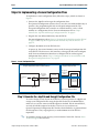
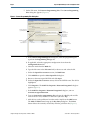
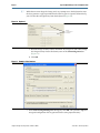
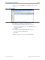
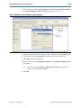
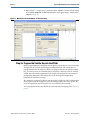
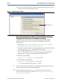
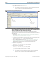
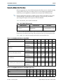
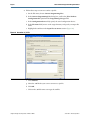
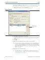
Using the Design Security Features in
Altera FPGAs
AN-556-2.1
Application Notes
This application note describes how you can use the design security features in
Altera® 40- and 28-nm FPGAs to protect your designs against unauthorized copying,
reverse engineering, and tampering of your configuration files. This application note
provides the hardware and software requirements for the 40- and 28-nm FPGAs
design security features. This application note also provides steps for implementing a
secure configuration flow.
1
This application note uses the term “40-nm” or “28-nm” FPGAs. Table 1 lists the
supported FPGAs and its applicable devices.
Table 1. Supported FPGAs
FPGA
Devices
Arria®
40 nm
28 nm
II and Stratix® IV
Stratix V, Arria V, and Cyclone® V
This application note covers the following topics:
■
“Overview of the Design Security Feature” on page 2
■
“Hardware and Software Requirements” on page 5
■
“Steps for Implementing a Secure Configuration Flow” on page 6
■
“Supported Configuration Schemes” on page 25
■
“Security Mode Verification” on page 27
■
“Serial FlashLoader Support with Encryption Enabled” on page 29
■
“JTAG Secure Mode for 28-nm FPGAs” on page 32
■
“US Export Controls” on page 32
In the highly competitive commercial and military environments, design security is
an important consideration for digital designers. As FPGAs start to play a role in
larger and more critical system components, it is ever more important to protect the
designs from unauthorized copying, reverse engineering, and tampering. FPGAs
address these concerns with the ability to decrypt a configuration bitstream using the
256-bit Advanced Encryption Standard (AES) algorithm, an industry standard
encryption algorithm.
101 Innovation Drive
San Jose, CA 95134
www.altera.com
© 2012 Altera Corporation. All rights reserved. ALTERA, ARRIA, CYCLONE, HARDCOPY, MAX, MEGACORE, NIOS,
QUARTUS and STRATIX words and logos are trademarks of Altera Corporation and registered in the U.S. Patent and Trademark
Office and in other countries. All other words and logos identified as trademarks or service marks are the property of their
respective holders as described at www.altera.com/common/legal.html. Altera warrants performance of its semiconductor
products to current specifications in accordance with Altera's standard warranty, but reserves the right to make changes to any
products and services at any time without notice. Altera assumes no responsibility or liability arising out of the application or use
of any information, product, or service described herein except as expressly agreed to in writing by Altera. Altera customers are
advised to obtain the latest version of device specifications before relying on any published information and before placing orders
for products or services.
ISO
9001:2008
Registered
June 2012 Altera Corporation
Subscribe
Page 2
Overview of the Design Security Feature
During device operation, FPGAs store configuration data in SRAM configuration
cells. Because SRAM memory is volatile, the SRAM cells must be loaded with
configuration data each time the device powers up. Configuration data is typically
sent from an external memory source, such as a flash memory or a configuration
device, to the FPGA. It is possible to intercept the configuration data when it is being
sent from the memory source to the FPGA. You can use the intercepted configuration
data to configure another FPGA.
FPGAs offer both volatile and non-volatile key storage. The key is stored in FPGAs
when using the design security feature. Depending on the security mode, you can
configure the FPGAs with a configuration file that is encrypted with the same key, or
for board testing, configure with a normal configuration file.
The design security feature is available when configuring the FPGAs with the fast
passive parallel (FPP) configuration mode with an external host (such as a MAX® II or
MAX V device or microprocessor) or when using active serial (AS) or passive serial
(PS) configuration schemes.
f For more information, refer to the Configuration, Design Security, and Remote System
Upgrades chapter in the respective device handbook.
Overview of the Design Security Feature
The design security feature for FPGAs protects against unauthorized copying, reverse
engineering, and tampering.
Table 2 lists some of the design approaches to make the solution secure.
Table 2. Design Security Approach for FPGAs
Design Approach
40-nm FPGA
28-nm FPGA
Non-volatile key
The non-volatile key is stored in polyfuses under layers of metals among other
polyfuses; thus determining the functionality of a particular fuse by simple visual
inspection is difficult. Moreover, additional physical security is designed around the
polyfuses to provide further security.
Configuration file readback
support
FPGAs do not support configuration file readback. This prevents attempts to read back
the configuration file after it is decrypted.
256-bit sequence requirement
Two 256-bit sequences are required to
generate the 256-bit key and to program
the key into the 40-nm FPGAs. You cannot
copy the FPGA design by programming a
256-bit key into another FPGA and
configuring it with an encrypted
configuration file. It is virtually impossible
to generate the two 256-bit sequences
from the key.
Non-volatile key with
tamper-protection bit set
For the non-volatile key with tamper-protection bit set, the polyfuses used to store the
key are non-volatile and one-time programmable. No battery is required. After the FPGAs
are programmed with the key, you can only configure the device with configuration files
encrypted with the same key. Attempts to configure the device with an unencrypted
configuration file or a configuration file encrypted with the wrong key results in
configuration failure. Therefore, tampering of the design file can be detected.
Using the Design Security Features in Altera FPGAs
Only one 256-bit key is generated and
programmed instead of the two 256-bit
sequences. The other 256 bits are hard
coded within the 28-nm FPGAs.
June 2012
Altera Corporation
Overview of the Design Security Feature
Page 3
Security Encryption Algorithm
FPGAs have a dedicated decryption block that uses the AES algorithm to decrypt
configuration data using a user-defined 256-bit key. Prior to receiving the encrypted
data, you must write the user-defined 256-bit key into the device.
The AES algorithm is a symmetrical block cipher that encrypts and decrypts data in
blocks of 256 bits. The encrypted data is subject to a series of transformations that
includes byte substitutions, data mixing, data shifting, and key additions.
FPGAs contain an AES decryptor block that uses the AES algorithm to decrypt the
configuration data prior to configuring the FPGA device. If the security feature is not
used, the AES decryptor is bypassed. The FPGAs AES implementation is validated as
conforming to the Federal Information Processing Standards FIPS-197.
f For more information about the AES algorithm, refer to the Federal Information
Processing Standards Publication FIPS-197 or the AES Algorithm (Rijndael) Information at
http://csrc.nist.gov.
f For more information about the AES validation for FPGAs, refer to the Advanced
Encryption Standard Algorithm Validation List published by the National Institute of
Standards and Technology (NIST) at http://csrc.nist.gov.
Non-Volatile and Volatile Key Storage
FPGAs offer both volatile and non-volatile key storage. The volatile key storage
requires battery backup to allow the key to be updated, while the non-volatile key
storage allows only one key to be programmed but does not require a battery.
1
Examples of lithium coin-cell type batteries that are used for volatile key storage
purposes are BR1220 (–30°C to +80°C) and BR2477A (–40°C to +125°C).
Table 3 lists a comparison of volatile and non-volatile key storage.
Table 3. Volatile and Non-Volatile Key Comparison
Option
Volatile Key
Non-Volatile Key
Key Length
256 bits
256 bits
Key Programmability
Reprogrammable and erasable key
One-time programmable key
Required
Not required
On-board
Both on-board and off-board
External Battery
Key Programming Method
Design
Protection (2)
(1)
Secure against copying, reverse engineering, and tampering
(3)
Notes to Table 3:
(1) Key programming is carried out through JTAG interface.
(2) The volatile key tamper-protection is only available for Arria II GX, Stratix V, Arria V, and Cyclone V devices.
(3) Tampering is prevented only when the volatile key tamper-protection bit is set, thus preventing configuration with unencrypted Programmer
Object Files (.pof) files.
June 2012 Altera Corporation
Using the Design Security Features in Altera FPGAs
Page 4
Overview of the Design Security Feature
c Enabling the tamper-protection bit disables the test mode in FPGAs. Disabling the test
mode is irreversible and prevents Altera from carrying out failure analysis. To enable
the tamper-protection bit, contact Altera Technical Support.
f For more information about the available security modes in the 40-nm and the 28-nm
FPGAs, refer to the Configuration, Design Security, and Remote System Upgrades chapter
of the respective device handbook.
Key Programming
Table 4 lists the four different methods for key programming.
Table 4. Key Programming Methods
Programming Procedure
On-Board Programming
Off-Board Programming
(1)
Method
Programming Tool
Prototyping
EthernetBlaster, JTAG
technologies, ByteBlaster™ II,
USB-Blaster™ (2)
Production
JTAG technologies
Prototyping
System General
(3)
Production
System General
(3)
Notes to Table 4:
(1) For information about programming support, contact Altera Technical Support.
(2) ByteBlaster II and USB-Blaster support only volatile key programming. EthernetBlaster and JTAG technologies
support both volatile and non-volatile key programming. For non-volatile key programming, you must regulate the
JTAG TCK pulse width (period) for proper poly-fuse programming.
(3) For 28-nm FPGAs, design security key programming support with System General tool is still pending availability
but is available for 40-nm FPGAs.
Key programming uses the following definitions:
■
On-board: procedure in which the device is programmed on your board
■
Off-board: procedure in which the device is programmed on a separate
programming system
■
Prototyping: method initially used to verify proper operation of a particular
method
■
Production: method used for large-volume production
Using the Design Security Features in Altera FPGAs
June 2012
Altera Corporation
Hardware and Software Requirements
Page 5
Hardware and Software Requirements
This section provides the hardware and software requirements for the FPGAs design
security feature. When using this feature, a volatile or non-volatile key is stored in the
FPGAs. The key is programmed before the FPGAs is configured and enters user
mode.
Hardware Requirements
Table 5 lists the voltage specifications that you must follow for a successful key
programming.
Table 5. Voltage Specifications for Design Security Feature
Parameter
TCK Period
Key Programming Mode
(1)
10 µs ± 1 µs
Ambient Temperature
Voltage (VCCBAT)
(2)
25°C ± 5°C
—
Notes to Table 5:
(1) This specification only applies for the non-volatile key programming. For the volatile key programming TCK period
specification, refer to the JTAG Specification section of the respective device datasheet.
(2) VCCBAT is a dedicated power supply for the volatile key storage and is not shared with other on-chip power supplies,
such as VCCIO or VCC. VCCBAT continuously supplies power to the volatile register regardless of the
on-chip supply condition. If you do not use the volatile key, connect the VCCBAT pin to either GND or a 3.0-V power
supply. For more information about the voltage specification, refer to the respective DC and Switching
Characteristics chapter or Device Datasheet.
1
After power up, you must wait for the device to exit POR before beginning the key
programming to ensure that VCCBAT is at its full rail. You may encounter verification
error when programing the volatile Encryption Key Programming (.ekp) file if you
have the VCCBAT pin tied to GND. The VCCBAT pin must to be tied to the
recommended VCCBAT voltage for proper operation.
f For more information about the POR specification in the FPGAs, refer to the POR
Specification section in the Configuration, Design Security, and Remote System Upgrades
chapter of the respective device handbook.
Software Requirements
To enable the design security feature of 40-nm FPGAs, you must use the Quartus® II
software version 9.0 or later. To enable the design security feature of
28-nm FPGAs, you must use the Quartus II software version 11.0 or later. To enable
the design security feature, you can obtain a license file from Altera Technical
Support.
June 2012 Altera Corporation
Using the Design Security Features in Altera FPGAs
Page 6
Steps for Implementing a Secure Configuration Flow
Steps for Implementing a Secure Configuration Flow
To implement a secure configuration flow, follow these steps, which are shown in
Figure 1:
1. Generate the .ekp file and encrypt the configuration data.
The Quartus II configuration software always uses the user-defined 256-bit key to
generate a key programming file and an encrypted configuration file. The
encrypted configuration file is stored in an external memory, such as a flash
memory or a configuration device. For more information, refer to “Step 1:
Generate the .ekp File and Encrypt Configuration File” on page 6.
2. Program the user-defined 256-bit key into the FPGAs.
For more information, refer to “Step 2a: Program the Volatile Key into the FPGAs”
on page 18 and “Step 2b: Program the Non-Volatile Key into the FPGAs” on
page 19.
3. Configure the 40-nm or 28-nm FPGA device.
At power up, the external memory source sends the encrypted configuration file
to the FPGAs. The devices use the stored key to decrypt the file and to configure
itself. For more information about how to configure FPGAs with encrypted
configuration data, refer to “Step 3: Configure the 40-nm or 28-nm FPGAs with
Encrypted Configuration Data” on page 25.
Figure 1. Secure Configuration Flow
Step 1. Generate the Encryption Key Programming File
Encrypt Configuration Data and Store in External Memory
Quartus II
Configuration
Data
AES
Encryptor
AES KEY
Encrypted
Configuration
Data
Encryption Key
Programming File
Step 3. Configure the Devices Using
Encrypted Configuration Data
Memory
Storage
Encrypted
Configuration
Data
Encrypted
Configuration
Data
FPGA
AES
Decryptor
Volatile and
Non-Volatile
Key Storage
AES KEY
Step 2. Program Key into Devices
Step 1: Generate the .ekp File and Encrypt Configuration File
To use the design security feature in the FPGAs, you must generate an .ekp file and
encrypt your configuration files using the Quartus II software (for 40-nm FPGAs,
make sure you use the same two 256-bit sequences for both. For the 28-nm FPGAs,
use only one 256-bit sequence for the key). The key is not saved into any
Quartus II-generated configuration files and the actual 256-bit key is generated from
the bit sequences. Thus, copying the key to another 40-nm or 28-nm FPGA is
impossible.
f To enable the design security feature, you must obtain a license file. Contact Altera
Technical Support for assistance.
Using the Design Security Features in Altera FPGAs
June 2012
Altera Corporation
Steps for Implementing a Secure Configuration Flow
Page 7
The .ekp file has different formats, depending on the hardware and system used for
programming. There are three file formats supported by the Quartus II software:
■
JAM Byte Code (.jbc) file
■
Jam™ Standard Test and Programming Language (STAPL) Format (.jam) file
■
Serial Vector Format (.svf) file
1
Only the .ekp file type is generated automatically from the Quartus II software. You
must create the .jam and .svf files using the Quartus II software if these files are
required in the key programming. The Quartus II software generates the JBC format
of the .ekp file in the same project directory.
1
Altera recommends that you keep the .ekp file confidential.
Use the .ekp file with the EthernetBlaster communications cable or USB-Blaster
download cable and the Quartus II software. The EthernetBlaster communications
cable can support both volatile and non-volatile key programming whereas the
USB-Blaster download cable is used only for volatile key programming. The .jam file
format is generally used with third-party programming vendors and JTAG
programmer vendors. The .svf file format is used with JTAG programmer vendors.
How to Generate the Single-Device .ekp File and Encrypt the Configuration
File using Quartus II Software
To generate a single-device .ekp file and encrypt your configuration file, follow these
steps:
1. Obtain a license file to enable the design security feature from Altera Technical
Support.
2. Start the Quartus II software.
3. On the Tools menu, click License Setup. The Options dialog box displays the
License Setup options.
4. In the License file field, enter the location and name of the license file, or browse
to and select the license file.
5. Click OK.
6. Compile your design with one of the following options:
a. On the Processing menu, click Start Compilation
b. On the Processing menu, point to Start and click Start Assembler.
An unencrypted SRAM Object File (.sof) is generated.
June 2012 Altera Corporation
Using the Design Security Features in Altera FPGAs
Page 8
Steps for Implementing a Secure Configuration Flow
7. On the File menu, click Convert Programming Files. The Convert Programming
Files dialog box appears (Figure 2).
Figure 2. Convert Programming Files Dialog Box
Select the appropriate
programming file type
Select the
appropriate mode
The file name for
the encrypted
configuration file
If applicable, select the
appropriate
configuration device
Add the unencrypted
SOF file for file conversion
Click to open
The SOF Files Properties:
Bitstream Encryption
dialog box
a. In the Convert Programming Files dialog box, select the programming file
type from the Programming file type list.
b. If applicable, select the appropriate configuration device from the
Configuration device list.
c. Select the mode from the Mode list.
d. Type the file name in the File name field, or browse to and select the file.
e. Under the Input files to convert section, click SOF Data.
f. Click Add File to open the Select Input File dialog box.
g. Browse to the unencrypted SOF file and click Open.
h. Under the Input files to convert section, click on the SOF file name. The field is
highlighted.
i. Click Properties. The SOF Files Properties: Bitstream Encryption dialog box
appears (Figure 3).
j.
In the SOF Files Properties: Bitstream Encryption dialog box, turn on
Generate encrypted bitstream.
k. Turn on Generate key programming file and type the .ekp file path and file
name in the text area, or browse to and select <filename>.ekp.
l. Add the keys to the pull-down list either with a .key file or the Add button.
The Add and Edit buttons bring up the Key Entry dialog box. The Delete
button deletes the currently selected key from the pull-down list (Figure 3).
Using the Design Security Features in Altera FPGAs
June 2012
Altera Corporation
Steps for Implementing a Secure Configuration Flow
Page 9
Figure 3. SOF File Properties: Bitstream Encryption Dialog Box
List the path and
file name for
the.ekp file
Agree and
acknowledge the
disclaimer
1
For 28-nm FPGA device, only one 256-bit key is generated and programmed instead
of the two 256-bit sequence. Only one key file is required for the 256-bit key. Unlike
the 40-nm FPGA device, the other 256-bits are hard coded within the 28-nm FPGAs.
Using the .key file option allows you to specify one or two key files in the
corresponding drop-down box. You may use different files for the Key 1 and Key 2
fields, or use one .key file for both. (Figure 4).
Figure 4. Use Key File Option
The .key file is a plain text file in which each line represents a key unless the line starts
with "#". The "#" symbol is used to denote comments.
June 2012 Altera Corporation
Using the Design Security Features in Altera FPGAs
Page 10
Steps for Implementing a Secure Configuration Flow
Each valid key line has the following format:
<key identity><white space><256-bit hexadecimal key>, as shown in Figure 5.
Figure 5. Example of a .key File
The key identity is an alphanumeric name that is used to identify the keys (similar to
the key file entry). The key is also the text displayed when the Show entered keys
button is turned off (Figure 6). It is displayed together with the full key when Show
entered keys is turned on (Figure 7).
Figure 6. Key Identity
Figure 7. Key Identity and the Full Key Entry
You can save the keys in the pull-down list to a .key file. You must click the
corresponding Save button to save a key and to display the standard File dialog box.
All keys in the pull-down list are saved to the selected or created .key file (Figure 4).
Using the Design Security Features in Altera FPGAs
June 2012
Altera Corporation
Steps for Implementing a Secure Configuration Flow
Page 11
Select the Key Entry Method to enter the encryption key either with the on-screen
keypad or keyboard (Figure 8).
Figure 8. Key Entry Method
The on-screen keypad allows you to enter the keys using the keypad shown in
Figure 9. Select a key and click on the on-screen keypad to enter values. You have the
option of allowing the keys to be shown as they are entered; if this option is used, you
do not need to confirm the keys.
Figure 9. On-Screen Keypad
Enter the
encryption key from
the on-screen keypad
June 2012 Altera Corporation
Using the Design Security Features in Altera FPGAs
Page 12
Steps for Implementing a Secure Configuration Flow
1
While the on-screen keypad is being used, any attempt to use the keyboard to enter
the keys generates a pop-up notification and the key press is ignored. Alternatively,
you can enter the encryption key from the keyboard (Figure 10).
Figure 10. Keyboard
Enter the
encryption key from
the keyboard
a. Read the design security feature disclaimer. If you agree to and acknowledge
the design security feature disclaimer, turn on the acknowledgement box
(Figure 11).
b. Click OK.
Figure 11. Example of User Interface
8. In the Convert Programming Files dialog box, click OK. The <filename>.ekp and
encrypted configuration file are generated in the same project directory.
Using the Design Security Features in Altera FPGAs
June 2012
Altera Corporation
Steps for Implementing a Secure Configuration Flow
Page 13
9. On the Tools menu, click Programmer. The Programmer dialog box appears
(Figure 12).
Figure 12. Programmer Dialog Box
10. In the Mode list, select JTAG as the programming mode.
11. Click Hardware Setup. The Hardware Setup dialog box appears.
a. In the currently selected hardware list, select EthernetBlaster as the
programming hardware.
b. Click Done.
12. Click Add File. The Select Programmer File dialog box appears.
a. Type <filename>.ekp in the File name field.
b. Click Open.
13. Highlight the .ekp file you added and click Program/Configure.
June 2012 Altera Corporation
Using the Design Security Features in Altera FPGAs
Page 14
Steps for Implementing a Secure Configuration Flow
14. On the File menu, point to Create/Update and click Create JAM, SVF, or ISC File.
The Create JAM, SVF or ISC File dialog box appears (Figure 13).
Figure 13. Create .jam File from Single-Device .ekp File
List the file
name for the
.jam file
Select the
.jam file format
15. Select the file format required (JEDEC STAPL Format [.jam]), for the .ekp file in
the File format field.
16. Type the file name in the File name field, or browse to and select the file.
17. Click OK to generate the .jam file.
18. On the Tools menu, click Programmer Options. The Programmer Options dialog
box appears (Figure 14).
Figure 14. Programmer Options Dialog Box
Option for volatile or
non-volatile
key programming
1
For non-volatile secure design feature, you must turn off the Configure volatile
design security key option to generate a non-volatile .svf file of the .ekp file
(Figure 14).
Using the Design Security Features in Altera FPGAs
June 2012
Altera Corporation
Steps for Implementing a Secure Configuration Flow
Page 15
19. Click OK.
20. Repeat Steps 15–17 to generate a .svf file of the .ekp file. Use the default setting in
the Create JAM, SVF, or ISC File dialog box when generating a .svf file of the .ekp
file (Figure 15).
Figure 15. Create .svf From Single-Device .ekp File
List the
file name
for the .svf file
Select the
.svf file format
How to Generate the Single-Device .ekp File and Encrypt Configuration File
Using Quartus II Software with the Command-Line Interface
There is a command-line interface that allows you to generate a single-device .ekp file
and encrypt Raw Binary File (.rbf). The command-line interface uses the Quartus II
software command-line executable, quartus_cpf, and requires the following syntax
or options:
■
--key/-k <path to key file>:<key identity>
■
A .sof file (user design)
■
An .ekp file (the required encryption key programming file name)
You can create a compressed and uncompressed .rbf for configuration by using the
following command with an option file which contains the string compression=on.
quartus_cpf -c --option=<option file> --key <keyfile>:<keyid1>:<keyid2>
<input_sof_file> <output_rbf_file>
You can learn more on the option file from the Quartus II software command line
help. Run quartus_cpf --help=option to learn more on the available options.
Example 1 shows two sets of keys that are stored in two different key files: key1 in
key1.key and key2 in key2.key.
Example 1.
quartus_cpf --key D:\SIV_DS\key1.key:key1 --key
D:\SIV_DS\key2.key:key2 D:\SIV_DS\test.sof D:\SIV_DS\test.ekp
June 2012 Altera Corporation
Using the Design Security Features in Altera FPGAs
Page 16
Steps for Implementing a Secure Configuration Flow
Example 2 shows two sets of keys that are stored in the same key file: key1 and key2
in key12.key.
Example 2.
quartus_cpf --key
D:\SIV_DS\key12.key:key1:key2 D:\SIV_DS\test.sof D:\SIV_DS\test.ekp
How to Generate the Multi-Device .ekp File and Encrypt the Configuration
File using Quartus II Software
Perform the following steps to generate a multi-device .ekp file and encrypt your
configuration file:
1. Start the Quartus II software.
2. Repeat Steps 9–11 in “How to Generate the Single-Device .ekp File and Encrypt the
Configuration File using Quartus II Software” on page 7.
3. Click Add File. The Select Programmer File dialog box appears.
a. Select the single-device .ekp file, and type <single_ekp>.ekp in the File name
field.
b. Click Open.
1
For the correct sequence of devices in the same JTAG chain, you can use the
Auto-Detect option in the Quartus II programmer. If one of the FPGAs is
not required to be key-programmed, you are not required to replace the
device with the <single_ekp>.ekp file in the Quartus II programmer.
4. Repeat Step 3 for the each device in the same chain. Ensure that the right device
sequence is used when adding the .ekp files to the programmer window.
5. Highlight all the .ekp files you added and click Program/Configure.
Using the Design Security Features in Altera FPGAs
June 2012
Altera Corporation
Steps for Implementing a Secure Configuration Flow
Page 17
6. On the File menu, point to Create/Update and click Create JAM, SVF, or ISC File.
The Create JAM, SVF, or ISC File dialog box appears (Figure 16).
Figure 16. Multi-Device Key Programming: .jam File Generation
Example of two
Stratix IV devices
in one JTAG
chain
Select the
.jam file format
7. Select the required file format (.jam), for all the .ekp files in the File format field.
8. Type the file name in the File name field, or browse to and select the file.
9. Click OK to generate the .jam file.
10. On the Tools menu, click Programmer Options. The Programmer Options dialog
box appears.
1
You must turn off Configure volatile design security key to generate a
non-volatile .svf file of the .ekp file.
11. Click OK.
June 2012 Altera Corporation
Using the Design Security Features in Altera FPGAs
Page 18
Steps for Implementing a Secure Configuration Flow
12. Repeat Steps 7–9 to generate a .svf file for all the .ekp files. Use the default setting
in the Create JAM, SVF, or ISC File dialog box when generating a .svf file of the
.ekp file (Figure 17).
Figure 17. Multi-Device Key Programming: .svf File Generation
Step 2a: Program the Volatile Key into the FPGAs
Before programming the volatile key into the FPGAs, ensure that you can successfully
configure the FPGA with an unencrypted configuration file. The volatile key is a
reprogrammable and erasable key. Before you program the FPGAs with the volatile
key, you must provide an external battery to retain the volatile key. FPGAs with the
volatile key successfully programmed can accept both encrypted and unencrypted
configuration bitstreams. This enables the use of unencrypted configuration
bitstreams for board-level testing.
Any attempt to configure the FPGAs containing the volatile key with a configuration
file encrypted with the wrong key causes the configuration to fail. If this occurs, the
nSTATUS signal from the FPGA pulses low and continues to reset itself.
You can program the key into the FPGAs with on-board prototyping from Table 4 on
page 4.
Using the Design Security Features in Altera FPGAs
June 2012
Altera Corporation
Steps for Implementing a Secure Configuration Flow
Page 19
Step 2b: Program the Non-Volatile Key into the FPGAs
Before programming the non-volatile key into the devices, ensure that you can
successfully configure the FPGA with an unencrypted configuration file. The
non-volatile key is one-time programmable through the JTAG interface. You can
program the non-volatile key into the devices without an external battery. Devices
with the non-volatile key successfully programmed can accept both encrypted and
unencrypted configuration bitstreams unless the tamper protection bit is set, in which
case only encrypted configuration bitstreams are accepted. This enables the use of
unencrypted configuration bitstreams for board-level testing.
Any attempt to configure the device containing the non-volatile key with a
configuration file encrypted with the wrong key causes the configuration to fail. If this
occurs, the nSTATUS signal from the FPGA pulses low and continues to reset itself.
You can program the non-volatile key into the devices using on-board prototyping,
volume production, and off-board prototyping and production solutions listed in
Table 4 on page 4.
Volatile or Non-Volatile Key Programming Using EthernetBlaster and
Quartus II Software
Connect the EthernetBlaster communications cable to the EthernetBlaster header as
shown in Figure 18.
f For additional information about connecting the EthernetBlaster communications
cable, refer to the EthernetBlaster Communications Cable User Guide.
Figure 18. EthernetBlaster Header (1),
(2)
EthernetBlaster Header
10 KΩ
10 KΩ
1 KΩ
J28
TCK
1
2
JTAG_CONN_TDO
3
4
JTAG_TMS
5
6
JTAG_CONN_TDI
7
8
9
10
VCC (3)
Notes to Figure 18:
(1) A 1-KΩ pull-down resistor is added to the TCK while 10-KΩ pull-up resistors are added to the TMS and TDI
signals for key programming.
(2) The EthernetBlaster header and USB-Blaster header are identical for key programming.
(3) For the specific voltages required using the JTAG download cable, refer to the Device Configuration, Secure Design
and Remote System Upgrades chapter of the respective device handbook.
June 2012 Altera Corporation
Using the Design Security Features in Altera FPGAs
Page 20
Steps for Implementing a Secure Configuration Flow
How to Perform Single-Device Volatile or Non-Volatile Key Programming
Using Quartus II Software
To perform single-device volatile or non-volatile key programming using the
Quartus II software through the EthernetBlaster, perform the following steps:
1. Check the firmware version of the EthernetBlaster. Verify that the JTAG firmware
build number is 101 or greater. If the version precedes build number 101, apply the
firmware upgrade.
1
Apply the firmware upgrade (EBFW100101.tar.gz) to the EthernetBlaster
unit. This updates the JTAG Firmware to Build 101. For firmware upgrade
instructions, refer to the EthernetBlaster Communications Cable User Guide.
2. Start the Quartus II software.
3. On the Tools menu, click Programmer. The Programmer dialog box appears
(Figure 19).
Figure 19. Key Programming Using EthernetBlaster and Quartus II Software
EthernetBlaster as
the programming
hardware
JTAG as the
programming mode
Add the <filename>.ekp file
4. In the Mode list, select JTAG as the programming mode (Figure 19).
Using the Design Security Features in Altera FPGAs
June 2012
Altera Corporation
Steps for Implementing a Secure Configuration Flow
Page 21
5. Click Hardware Setup. The Hardware Setup dialog box appears.
a. In the Currently selected hardware list, select EthernetBlaster as the
programming hardware.
b. Click Done.
6. Click Add File. The Select Programmer File dialog box appears.
a. Type <filename>.ekp in the File name field.
b. Click Open.
7. Highlight the .ekp file you added and click Program/Configure (Figure 20).
Figure 20. Programming the Key
Click Start to
program the key
Highlight the file and click
Program/Configure
8. On the Tools menu, click Options. The Options dialog box appears (Figure 21).
9. In the Category list, click Programmer. You can choose to turn on or turn off the
Configure volatile design security key option to perform volatile or non-volatile
key programming.
10. Click OK to close the Options dialog box.
11. Click Start to program the key.
June 2012 Altera Corporation
Using the Design Security Features in Altera FPGAs
Page 22
Steps for Implementing a Secure Configuration Flow
12. The Quartus II software message window provides information about the success
or failure of the key programming operation.
Figure 21. Programming Options Window
Option for volatile or
non-volatile key programming
How to Perform Single-Device Volatile or Non-Volatile Key Programming
Using Quartus II Software with the Command-Line Interface
To perform single-device volatile or non-volatile key programming using the
Quartus II command-line interface through the EthernetBlaster, perform the
following steps:
1. Perform Step 1 of “How to Perform Single-Device Volatile or Non-Volatile Key
Programming Using Quartus II Software” on page 20.
2. To determine the EthernetBlaster cable port number that is connected to the JTAG
server, type quartus_jli -n at the command-line prompt.
3. With the single_ekp.jam file generated in “Step 1: Generate the .ekp File and
Encrypt Configuration File” on page 6, execute volatile or non-volatile key
programming to a single FPGA with the following command line:
■
Volatile key programming:
quartus_jli -c<n> single_ekp.jam -aKEY_CONFIGURE
■
Non-volatile key programming:
quartus_jli -c<n> single_ekp.jam -aKEY_PROGRAM
<n> is the port number returned with the -n option.
1
The Quartus II software command-line executable provides information about the
success or failure of the key programming operation.
f For more information about quartus_jli, refer to the Using the Command-Line
Executable in Quartus II Software section in AN425: Using Command-Line Jam STAPL
Solution for Device Programming.
Using the Design Security Features in Altera FPGAs
June 2012
Altera Corporation
Steps for Implementing a Secure Configuration Flow
Page 23
How to Perform Multi-Device Volatile or Non-Volatile Key Programming Using
Quartus II Software
To perform multi-device volatile or non-volatile key programming using the
Quartus II software through the EthernetBlaster, perform the following steps:
1. Repeat Steps 1–5 in “How to Perform Single-Device Volatile or Non-Volatile Key
Programming Using Quartus II Software” on page 20.
2. Click Add File. The Select Programmer File dialog box appears (Figure 19).
a. Programming using single-device .ekp files:
i. Type <single_device>.ekp in the File name field.
ii. Click Open.
iii. Repeat Steps i–ii for the number of devices in the same chain.
iv. Highlight the .ekp files you added and click Program/Configure
(Figure 22).
1
For the correct sequence of the devices in the same JTAG chain, you can use
the Auto-Detect option in the Quartus II programmer.
Figure 22. Multi-Device Key Programming with .ekp Files
Example of two
Stratix IV devices
in one JTAG chain
selected for key
programming
Ensure the right
device sequence is used
b. Programming using a multi-device .jam file:
i. Type <multi_device>.jam in the File name field.
ii. Click Open.
iii. Highlight the .jam file you added and click Program/Configure
(Figure 23).
3. Repeat Steps 8–10 of “How to Perform Single-Device Volatile or Non-Volatile Key
Programming Using Quartus II Software” on page 20 to perform volatile or
non-volatile key programming.
June 2012 Altera Corporation
Using the Design Security Features in Altera FPGAs
Page 24
Steps for Implementing a Secure Configuration Flow
4. Click Start to program the key (Figure 23).
1
The Quartus II software message window provides information about the
success or failure of the key programming operation.
Figure 23. Multi-Device Key Programming with .jam Files
Click Start to
program the key
Highlight the file and click
Program/Configure
How to Perform Multi-Device Volatile or Non-Volatile Key Programming Using
Quartus II Software with the Command-Line Interface
To perform multi-device volatile or non-volatile key programming using the
Quartus II software command-line interface through the EthernetBlaster, perform the
following steps:
1. Perform Step 1 of “How to Perform Single-Device Volatile or Non-Volatile Key
Programming Using Quartus II Software” on page 20.
2. To determine the EthernetBlaster cable port number that is connected to the JTAG
server, type quartus_jli -n at the command-line prompt.
3. With the multi_ekp.jam file generated in “Step 1: Generate the .ekp File and
Encrypt Configuration File” on page 6, execute volatile or non-volatile key
programming for multiple FPGAs with the following command-line:
■
Volatile key programming:
quartus_jli -c<n> multi_ekp.jam -aKEY_CONFIGURE
■
Non-volatile key programming:
quartus_jli -c<n> multi_ekp.jam -aKEY_PROGRAM
<n> is the port n umber returned with the -n option.
1
The Quartus II software command-line interface provides information
about the success or failure of the key programming operation.
Using the Design Security Features in Altera FPGAs
June 2012
Altera Corporation
Supported Configuration Schemes
Page 25
Key Programming Using JTAG Technologies
The key programming for your design is performed using a .svf file (.ekp file in .svf
format) and a JT 37xx boundary scan controller in combination with a JT 2147
QuadPod system.
f Procedures for JTAG programming are found on the JTAG Technologies website at
www.jtag.com.
Information about creating a .svf file to support multi-device programming is
described in “How to Generate the Multi-Device .ekp File and Encrypt the
Configuration File using Quartus II Software” on page 16.
Step 3: Configure the 40-nm or 28-nm FPGAs with Encrypted Configuration
Data
The final step is to configure the protected 40-nm or 28-nm FPGAs with the encrypted
configuration file.
During configuration, the encrypted configuration data is sent to the 40-nm or 28-nm
FPGAs. Using the previously stored key, the FPGA decrypts the configuration data
and uses the unencrypted data to configure itself. Only configuration files encrypted
using the correct key are accepted by the FPGA for successful configuration. Without
a correct key, a stolen encrypted file is useless.
Supported Configuration Schemes
The design security feature is available in all configuration methods except
JTAG-based configuration. Therefore, you can use the design security feature in FPP
mode (when using an external controller, such as a MAX II or MAX V device or a
microprocessor and a flash memory), or in AS and PS configuration schemes.
f For more information about the supported configuration scheme in design security,
refer to the Configuration, Design Security, and Remote System Upgrades chapter of the
respective device handbook.
Table 6 lists the configuration schemes that support the design security feature.
Table 6. Availability of Security Configuration Schemes (Part 1 of 2)
Configuration Scheme
Configuration Method
Design Security
v
(1)
FPP
MAX II or MAX V device or
microprocessor, and flash
memory
AS
Serial configuration device
v
PS
MAX II or MAX V device or
microprocessor, and flash
memory
v
Download cable
June 2012 Altera Corporation
v
(2)
Using the Design Security Features in Altera FPGAs
Page 26
Supported Configuration Schemes
Table 6. Availability of Security Configuration Schemes (Part 2 of 2)
Configuration Scheme
JTAG
Configuration Method
Download cable
Design Security
—
(3)
Notes to Table 6:
(1) In this mode, the host system must send a DCLK signal that is 4x the data rate.
(2) The MicroBlaster™ tool is required to execute encrypted PS configuration using a .rbf through ByteBlaster II or
ByteBlasterMV™ download cable. For more information about configuration, refer to the Configuration Center.
(3) For volatile key programming only.
1
For more information the MAX II or MAX V device and flash memory configuration
method, refer to the MAX Series Configuration Controller Using Flash Memory White
Paper.
In addition, if your system contains a common flash interface (CFI) flash memory, you
can use it for the FPGA configuration as well. The MAX II and MAX V parallel flash
loader (PFL) feature provides an efficient method to program CFI flash memory
through the JTAG interface.
f For more information about PFL, refer to the Parallel Flash Loader Megafunction User
Guide.
You can use the design security feature with other configuration features, such as the
compression and remote system upgrade features. When compression is used with
the design security feature, the configuration file is first compressed and then
encrypted in the Quartus II software. During configuration, the FPGA first decrypts
and then uncompresses the configuration file.
You can either perform boundary-scan test (BST) or use the SignalTap II logic analyzer
to analyze functional data within the FPGA. However, JTAG configuration is not
possible after the key with tamper-protection bit set is programmed into the 40-nm or
28-nm FPGAs.
When using the SignalTap II logic analyzer, you must first configure the device with
an encrypted configuration file using PS, FPP, or AS configuration modes. The design
must contain at least one instance of the SignalTap II logic analyzer. After the FPGA is
configured with a SignalTap II logic analyzer instance in the design and after the
SignalTap II logic analyzer window is opened in the Quartus II software, simply scan
the chain and the SignalTap II logic analyzer is now ready to acquire data over JTAG
interface.
Using the Design Security Features in Altera FPGAs
June 2012
Altera Corporation
Security Mode Verification
Page 27
Security Mode Verification
FPGAs support the KEY_VERIFY JTAG instruction that allows you to verify the existing
security mode of the device. To check if you have successfully programmed the
volatile key, use the .jam files to automate the security mode verification steps.
f For more information about the available security modes in the FPGAs, refer to the
“Security Design” section in the in the Configuration, Design Security, and Remote
System Upgrades chapter of the respective device handbook.
Table 7 lists the KEY_VERIFY JTAG instruction.
Table 7. KEY_VERIFY JTAG Instruction
JTAG Instruction
Instruction Code
Description
Connects the key verification
scan register between TDI and
TDO.
00 0001 0011
KEY_VERIFY
KEY_VERIFY JTAG instruction allows you to read out the information on the security
features that are enabled on the chip. This instruction scans out associated bit values.
Table 8 and Table 9 lists the security mode and the associated bit value.
Table 8. Security Mode Verification for 40-nm FPGAs
Security Mode
Supported Device
Bit 0
Bit 1
Bit 2
Bit 3
Bit 4
Bit 5
0
0
0
0
0
0
0
0
0
0
NA
NA
1
0
0
0
0
0
1
0
0
0
NA
NA
1
0
0
0
1
0
NA
NA
NA
NA
NA
NA
0
1
0
1
0
0
0
1
0
1
NA
NA
0
1
1
1
0
0
0
1
1
1
NA
NA
Arria II GX
No key
■
Arria II GZ
■
Stratix IV
Arria II GX
Volatile key
■
Arria II GZ
■
Stratix IV
Arria II GX
Volatile key with tamper protection
■
Arria II GZ
■
Stratix IV
Arria II GX
Non-volatile key
■
Arria II GZ
■
Stratix IV
Arria II GX
Non-volatile key with tamper protection bit
■
Arria II GZ
■
Stratix IV
Table 9. Security Mode Verification for 28-nm FPGAs (Part 1 of 2)
Security Mode
Bit 0
Bit 1
Bit 2
Bit 3
Bit 4
Bit 5
Bit 6
Bit 7
Bit 8
No key
0
0
0
0
0
0
0
0
0
Volatile key
1
0
0
0
1
1
0
0
1
Volatile key with tamper protection
1
0
0
0
1
1
1
0
1
June 2012 Altera Corporation
Using the Design Security Features in Altera FPGAs
Page 28
Security Mode Verification
Table 9. Security Mode Verification for 28-nm FPGAs (Part 2 of 2)
Security Mode
Bit 0
Bit 1
Bit 2
Bit 3
Bit 4
Bit 5
Bit 6
Bit 7
Bit 8
Non-volatile key
0
1
1
1
0
1
0
0
0
Non-volatile key with tamper protection bit
0
1
1
1
0
1
0
0
0
Example 3, Example 4, and Example 5 show the .jam files to verify the FPGAs
security modes.
Example 3. JAM File for 40-nm FPGAs (Arria II GX Devices)
STATE RESET;
STATE IDLE;
'Security Mode Identification
BOOLEAN verify_reg[6];
IRSCAN 10, $013;
WAIT 100 USEC;
DRSCAN 6, $0, CAPTURE verify_reg[5..0];
Example 4. JAM File for 40-nm FPGAs (Arria II GZ and Stratix IV Devices)
STATE RESET;
STATE IDLE;
'Key Verification
BOOLEAN verify_reg[4];
IRSCAN 10, $013;
WAIT 100 USEC;
DRSCAN 4, $0, CAPTURE verify_reg[3..0];
Example 5. JAM File for 28-nm FPGAs
STATE RESET;
STATE IDLE;
'Key Verification in JAM format
BOOLEAN verify_reg[9];
IRSCAN 10, $013;
WAIT 100 USEC;
DRSCAN 9, $0, CAPTURE verify_reg[8..0];
Using the Design Security Features in Altera FPGAs
June 2012
Altera Corporation
Serial FlashLoader Support with Encryption Enabled
Page 29
Serial FlashLoader Support with Encryption Enabled
Altera provides an in-system programming solution for serial configuration devices
called Serial FlashLoader (SFL). The SFL megafunction is available with the Quartus II
software version 6.0 SP1 or later. You can instantiate the SFL block to your design and
have the flexibility to update your design stored in the serial configuration device
without reprogramming the configuration device through the AS interface.
As long as the JTAG interface of the FPGA is accessible, you can use the SFL solution
for your application. If the design security feature with tamper-protection bit is set,
the SFL solution does not work. Although the JTAG programming is not supported
when the tamper-protection bit is set, you may instantiate the SFL megafunction in
your design and execute the SFL programming for the first time before non-volatile
key programming with the tamper protection bit is set in the FPGA.
To use the SFL megafunction with the encryption feature enabled in a single FPGA
device chain, follow these steps:
1. Start the Quartus II software.
2. Instantiate the SFL megafunction in your FPGA top-level design.
f For more information about instantiating the SFL megafunction, refer to the
Instantiating SFL Megafunction in the Quartus II Software section in
AN 370: Using the Serial FlashLoader With the Quartus II Software.
3. Compile your design with one of the following options. An unencrypted .sof is
generated.
a. On the Processing menu, click Start Compilation.
or
b. On the Processing menu, point to Start and click Start Assembler.
June 2012 Altera Corporation
Using the Design Security Features in Altera FPGAs
Page 30
Serial FlashLoader Support with Encryption Enabled
4. Follow these steps to convert a .sof to a .jic file:
a. On the File menu, choose Convert Programming Files.
b. In the Convert Programming Files dialog box, scroll to the JTAG Indirect
Configuration File (.jic) from the Programming file type field.
c. In the Configuration device field, specify the serial configuration device.
d. In the File name field, browse to the target directory and specify an output file
name.
e. Highlight the .sof data in the Input files to convert section (Figure 24).
Figure 24. Generation of .jic File
f. Click Add File.
g. Select the .sof file that you want to convert to a .jic file.
h. Click OK.
i. Click on the .sof file name to encrypt the .sof file.
Using the Design Security Features in Altera FPGAs
June 2012
Altera Corporation
Serial FlashLoader Support with Encryption Enabled
Page 31
To encrypt the .sof file, refer to Step 7 in “How to Generate the Single-Device .ekp
File and Encrypt the Configuration File using Quartus II Software” on page 7.
j.
Highlight FlashLoader and click Add Device (Figure 25).
Figure 25. FlashLoader
Add the FlashLoader
bridge of the required
FPGA
k. Click OK. The Select Devices page appears.
l. Select the target FPGA that you are using to program the serial configuration
device.
m. Click OK.
5. Program the serial configuration device with the encrypted .jic file.
f For more information about programming the serial configuration device
or devices with the .jic file that you just created, refer to the procedure in
the Programming Serial Configuration Devices Using the Quartus II Programmer
and JIC Files section in AN 370: Using the Serial FlashLoader With the
Quartus II Software.
6. Program the key into the FPGA device.
1
June 2012 Altera Corporation
To program the key to a single FPGA device, follow the steps in“How to
Perform Single-Device Volatile or Non-Volatile Key Programming Using
Quartus II Software” on page 20.
Using the Design Security Features in Altera FPGAs
Page 32
JTAG Secure Mode for 28-nm FPGAs
7. The encrypted FPGA is then configured by the programmed serial configuration
device.
1
To program the key with a .jam file, you must convert the .jic file to a .jam
file.
f For more information about converting a .jic file to a .jam file, refer to the
Converting JIC Files to JAM Files in the Quartus II Software section in AN 370:
Using the Serial FlashLoader With the Quartus II Software.
f For more information about the timing parameters for PS and FPP configuration
schemes with the design security feature enabled in FPGAs, refer to the Configuration,
Design Security, and Remote System Upgrades chapter of the respective device
handbook.
JTAG Secure Mode for 28-nm FPGAs
When you enable the tamper-protection bit, 28-nm FPGAs are in JTAG secure mode
after power up. During JTAG secure mode, many JTAG instructions are disabled.
28-nm FPGAs only allow you to exercise mandatory JTAG 1149.1 and 1149.6
instructions. These instructions are SAMPLE/PRELOAD, BYPASS, EXTEST, and optional
instructions such as IDCODE and SHIFT_EDERROR_REG.
To enable the access of other JTAG instructions such as USERCODE, HIGHZ, CLAMP,
PULSE_NCONFIG, and CONFIG_IO, you must issue the UNLOCK instruction to deactivate
the JTAG secure mode. You can issue the LOCK instruction to put the device back into
JTAG secure mode. You can only issue both the LOCK and UNLOCK instructions during
user mode.
f For more information about the JTAG binary instruction code related to the LOCK and
UNLOCK instructions, refer to the JTAG Boundary-Scan Testing chapter of the respective
device handbook.
US Export Controls
The US export controls for the FPGAs are generally classified under the US Export
Control Classification Numbers (ECCN) 3A001.a.7 or 3A991.d. Although FPGAs
perform decryption, the export control classification of the devices does not change as
the decryption capability is only used to protect the configuration bitstream. Altera’s
Quartus II software development tools (version 9.0 or later), which encrypt the
configuration bitstream, are formally classified under US ECCN 5D002 c.1 and subject
to export under license exception ENC as a “retail” commodity to most countries. You
may contact [email protected] for any export-related questions.
Using the Design Security Features in Altera FPGAs
June 2012
Altera Corporation
Document Revision History
Page 33
Document Revision History
Table 10 lists the revision history for this application note.
Table 10. Document Revision History
Date
June 2012
June 2011
June 2009
March 2009
Version
2.1
2.0
1.1
1.0
June 2012 Altera Corporation
Changes
■
Updated Table 1 and Table 3.
■
Updated .ekp file verification error information.
■
Updated “Hardware Requirements” section.
■
Updated application note for the Quartus II software version 11.0 release.
■
Changed specific device names to 40- or 28-nm FPGAs.
■
Added “Security Mode Verification” and “JTAG Secure Mode for 28-nm FPGAs” sections.
■
Added Table 1
■
Updated Table 5.
■
Added Example 3, Example 4, and Example 5
■
Updated Figure 1.
■
Minor text edits.
■
Updated “Introduction” on page 1.
■
Updated “Overview of the Design Security Feature” on page 2.
■
Updated “Security Encryption Algorithm” on page 2.
■
Updated “Non-Volatile and Volatile Key Storage” on page 3.
■
Updated (Note 3) of Table 2 on page 4.
■
Updated “Hardware and Software Requirements” on page 4.
■
Updated (Note 1) of Table 3 on page 5.
■
Updated “Steps for Implementing a Secure Configuration Flow” on page 5.
■
Updated “Step 2a: Program the Volatile Key into the Arria II GX or Stratix IV Devices” on
page 17.
■
Updated “Step 2b: Program the Non-Volatile Key into the Arria II GX or Stratix IV Devices”
on page 18.
■
Updated “Step 3: Configure the Arria II GX or Stratix IV Devices with Encrypted
Configuration Data” on page 24.
■
Added Table 3 on page 28.
■
Updated Figure 1 on page 6 and Figure 26 on page 29.
Initial release.
Using the Design Security Features in Altera FPGAs
Page 34
Using the Design Security Features in Altera FPGAs
Document Revision History
June 2012
Altera Corporation