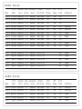
1
F C C I n f o rm ati o n
Federal Communications Commission Radio Frequency Interference Statement
This equipment has been tested and found to comply with the limits for a Class B Digital Device, pursuant to Part
15 of the FCC Rules. These limits are designed to provide reasonable protection against harmful interference in a
residential installation. This equipment generates, uses and can radiate radio frequency energy and, if not installed
and used in accordance with the instructions, may cause harmful interference to radio communication. However,
there is no guarantee that interference will not occur in a particular installation. If this equipment does cause
harmful interference to radio or television reception, which can be determined by turning the equipment off and on,
the user is encouraged to try to correct the interference by one or more of the following measures:
• Reorient or relocate the receiving antenna.
• Increase the distance between the equipment and receiver.
• Connect the equipment to an outlet on a circuit different from that to which the receiver is connected.
• Consult the dealer or an experienced radio/TV technician for help.
Changes or modifications not expressly approved by the mainboard manufacturer could void the user’s authority to
operate this equipment. To ensure compliance the subject device must use shielded interface cables.
Version 1.01
Copyright © September 1996 All rights reserved
This publication may not be copied, reproduced, translated, transmitted or reduced to
any printed or electronic medium or to any machine readable form, or stored in a
retrieval system, either in whole or in part without the written consent of the copyright holders.
The contents of this publication are subject to change. The manufacturer reserves the
right to alter the contents of this publication at any time and without notice. The
contents of this publication may contain inaccuracies or typographical errors and is
supplied for informational use only.
Products are noted in this publication for identification purposes only. Microsoft is a
registered trademark and W indows is a trademark of Microsoft Corporation. Pentium
is a trademark of Intel Corporation. All other product names or brands may be trademarks or registered trademarks of their respective holders.
Part No.: MN–083–B11–81
Contents
Introduction ............................................................................................................................................................................................................... 1 –1
Manual Features .............................................................................................................................................................................................. 1 –1
Package Contents ........................................................................................................................................................................................... 1 –2
Feature Summary ........................................................................................................................................................................................... 1 –2
Static Electric Discharge Precautions ........................................................................................................................................... 1 –4
Hardware Configuration ..................................................................................................................................................................................... 2 –1
Configuration Quick Reference ................................................................................................................................................................ 2 –1
CPU Configuration & Installation .................................................................................................................................................. 2 –1
CPU Voltage ..................................................................................................................................................................................... 2 –1
External Clock Frequency & External Clock Factor .................................................................................................... 2 –3
DRAM Installation .................................................................................................................................................................................. 2 –7
DIMM Voltage Settings .............................................................................................................................................................. 2 –8
Onboard Connectors ...................................................................................................................................................................................... 2 –9
Drive Controller & I/O Port Connectors .................................................................................................................................... 2 –9
System Enclosure Connectors ...................................................................................................................................................... 2 –1 2
Other Connectors ................................................................................................................................................................................. 2 –1 4
Power Input Connector ........................................................................................................................................................... 2 –1 4
Keyboard & PS/2 Mouse Connectors ........................................................................................................................... 2 –1 4
IDE Activity LED Connector .................................................................................................................................................... 2 –1 4
CPU Fan Power Connector .................................................................................................................................................... 2 –1 4
PR5 Hardware Configuration ................................................................................................................................................................. 2 –1 6
CPU Options & Installation ............................................................................................................................................................ 2 –1 6
Related Terminology ................................................................................................................................................................. 2 –1 6
CPU Settings ................................................................................................................................................................................. 2 –1 8
System Memory Configuration ................................................................................................................................................... 2 –2 6
DIMM Voltage Settings ........................................................................................................................................................... 2 –2 9
Installing Memory Modules ........................................................................................................................................................... 2 –3 0
Level 2 Cache Options ..................................................................................................................................................................... 2 –3 2
Onboard Connectors ................................................................................................................................................................................... 2 –3 3
Disk Drive Controller & I/O Port Connectors ...................................................................................................................... 2 –3 3
System Enclosure Connectors ...................................................................................................................................................... 2 –3 5
Other Connectors ................................................................................................................................................................................. 2 –3 5
Power Input Connector ........................................................................................................................................................... 2 –3 5
Keyboard & PS/2 Mouse Connectors ........................................................................................................................... 2 –3 5
IDE Activity LED Connector .................................................................................................................................................... 2 –3 7
CPU Fan Power Connector .................................................................................................................................................... 2 –3 7
DIP Switch & Jumper Summary ................................................................................................................................................. 2 –3 8
JP3: Clear CMOS Memory .................................................................................................................................................... 2 –3 9
JP8: Flash ROM Type ............................................................................................................................................................... 2 –4 0
Software Configuration....................................................................................................................................................................................... 3 –1
The BIOS CMOS Setup Utility .................................................................................................................................................................. 3 –1
Accessing The CMOS Setup Utility................................................................................................................................................ 3 –1
Standard CMOS Setup ........................................................................................................................................................................ 3 –4
BIOS Features Setup ............................................................................................................................................................................ 3 –8
Chipset Features Setup .................................................................................................................................................................... 3 –1 3
Power Management Setup ............................................................................................................................................................ 3 –1 4
PCI & Onboard I/O Setup ............................................................................................................................................................. 3 –1 8
Load BIOS Defaults ............................................................................................................................................................................ 3 –2 2
Load Setup Defaults .......................................................................................................................................................................... 3 –2 3
Password Setting ................................................................................................................................................................................ 3 –2 4
IDE HDD Auto Detection .................................................................................................................................................................. 3 –2 5
HDD Low Level Format .................................................................................................................................................................... 3 –2 5
Save And Exit Setup .......................................................................................................................................................................... 3 –2 5
Exit Without Saving ........................................................................................................................................................................... 3 –2 5
Updating The BIOS ...................................................................................................................................................................................... 3 –2 5
IDE Driver Disk ............................................................................................................................................................................................... 3 –2 5
Technical Information .......................................................................................................................................................................................... 4 –1
CPU Specifications .......................................................................................................................................................................................... 4 –1
Intel CPUs ................................................................................................................................................................................................... 4 –2
AMD K5 CPUs ........................................................................................................................................................................................... 4 –9
Cyrix CPUs ............................................................................................................................................................................................... 4 –1 0
IDE Installation Guide ................................................................................................................................................................................ 4 –1 1
IDE Transfer Modes ............................................................................................................................................................................ 4 –1 1
Installing IDE Devices ........................................................................................................................................................................ 4 –1 2
IDE Cables ...................................................................................................................................................................................... 4 –1 2
Example IDE Configurations .......................................................................................................................................................... 4 –1 2
BIOS Setup ............................................................................................................................................................................................. 4 –1 7
IDE Hard Disk Formatting ............................................................................................................................................................... 4 –1 7
Technical Support ......................................................................................................................................................................................... 4 –1 8
Troubleshooting Guidelines ............................................................................................................................................................ 4 –1 8
The Troubleshooting Form .............................................................................................................................................................. 4 –1 9
Introduction
This manual has the information you will need to install,
configure and use your PR5 mainboard. This section covers manual features, what is included in the PR5 package
and a summary of the PR5’ s features.
M an u al F e atu re s
Manual Features
Package Contents
Feature Summary
This manual is designed to present information in both
summary and detail so that whether you are unfamiliar
with a topic or just need to get some specific information, you can find what you need with a minimum of
effort. The summarized information is intended for experienced users. Please refer to the detailed explanations
if you are unfamiliar with a topic.
A list of the main topics in each section appears in the
sidebar on the first page. The manual is divided into four
sections:
Section 1: Introduction
Section 2: Hardware Configuration
Section 3: Software Configuration
Section 4: Technical Information
Illustrations and tables identify locations and settings and
sidebar notes and pointers are used to highlight important information.
Sidebar Notes
Summary information, tips and important points generally are in the sidebar on the left side of the page. If the
information in the sidebar is not sufficient for you, check
the main text nearby for additional information or refer
to the component location noted in the sidebar.
Pointers
Cautions, important information, tips and key points are
highlighted by the following icons:
!
☞
Section 1
Cautions & Important Information
Tips & Key Points
P ac k ag e C o n t e n ts
If your PR5 is already installed in a system you can skip
this section. If you are installing the PR5 yourself, please
check and make sure that all items listed are present and
undamaged. If anything is missing or damaged, please
contact your vendor for instructions.
The PR5 package contains the following items:
•
PR5 mainboard
•
Cable pack including:
1 Parallel cable/port assembly
1 Dual serial cable/port assembly
1 Floppy controller ribbon cable
2 IDE controller ribbon cables
1 USB cable/port assembly (optional)
•
Support Disk floppy disk
•
User’ s Manual
The cables connect to the port and controller connector
headers on the mainboard. This is explained in Section 2.
The Support Disk has drivers for use with various operating systems. These are covered in Section 3.
Feature Summary
The PR5 mainboard incorporates a variety of performance-enhancing features and is designed for use in File
Server and Workstation computers and other high-end
applications. It uses Intel’ s 430VX chipset, its PCI expansion bus supports the concurrent PCI 2.1 standard and it
has two Universal Serial Bus (USB) ports.
The memory subsystem includes an upgradable 256KB
Pipeline Burst Level 2 cache and support for both 72-pin
Fast Page Mode (FPM) and EDO SIMM memory modules as well as 168-pin DIMM modules. This design supports both current memory standards and provides an
upgrade path to future high-performance 64-bit memory.
The PR5’ s feature list includes:
CPU Support – Socket 7 ZIF socket for Pentium and compatible CPUs as follows:
•
Intel Pentium 75 – 200MHz CPUs
•
AMD AMD-K5 75 – 100MHz CPUs
•
Cyrix 6x86 P120+, 133+, 150+ and 166+ CPUs
•
Future Pentium-class CPUs
Chipset – Intel 430VX:
•
Incorporates concurrent PC Rev. 2.1 for enhanced
interface card speed
L2 Cache – Pipeline Burst Level 2 cache:
•
256KB onboard
•
Upgradable to 512KB using COAST module in
upgrade socket
System DRAM – Expandable up to 128MB in multiple
configurations (no DIMM sockets on PR5B):
•
Four 72-pin sockets for Fast Page or EDO DRAM
SIMM memory modules
•
Two 16 8-p in s ock ets f or F ast Pag e, ED O or
SDRAM DIMM memory modules
•
Supports Intel-specified 3.3V Unbuffered DRAM
for DIMM modules
System BIOS – Award BIOS with support for:
•
Plug and Play
•
Advanced Power Management
•
DMI (Desktop Management Interface) features including system suspend
Onboard Multi I/O – Onboard I/O ports and disk controllers including:
•
Two Universal Serial Bus (USB) ports
•
One EPP/ECP bidirectional parallel port
•
Two high-speed 16550-compatible serial ports
•
Floppy disk controller supports 360KB, 720KB,
1.2MB, 1.44MB and 2.88MB formats
•
Enhanced IDE hard disk controller supports PIO
Mode 0 – 4 and Bus Mastering
Additional Features – Other features include:
•
“ AT” dimensions for ease of installation
•
Expansion bus with four ISA and three PCI slots
•
Support for the 3-Mode floppy disk standard
•
Can boot from either of two hard disk drives allowing support for dual operating systems
Static Electric Discharge Precautions
Static electric discharge can deliver a high-voltage shock
to the mainboard sufficient to damage or destroy components on the board. Because of this, it is important to
observe precautions when you handle the mainboard and
any devices you install on it, including the CPU, memory
modules and expansion cards.
There are several simple precautions you can take:
•
Use an anti-static wrist strap, which can be purchased inexpensively from most computer stores.
Connect the strap lead to a grounded metallic object and put on the strap before touching any components.
•
Put components on an anti-static pad or keep them
in their anti-static packaging until you install them.
•
If you don’ t have a wrist strap or pad, make sure
to touch a metallic object such as the system case
to ground yourself before handling any components.
PR5 Mainboard Layout Key
1. ISA Bus Expansion Slots
2. PCI Bus Expansion Slots
3. USB Port Connector
4. Floppy Disk Drive Controller Connector
5. IDE Controller Connectors IDE1 (left) & IDE2 (right)
6. PS/2 Mouse (left) & Keyboard (right) Connectors
7. Power Input Connectors
8. COM1 (left) & COM2 (right) Serial, LPT Parallel Port Connectors
9. SIMM Memory module sockets 1 – 4 (left to right)
10. DIMM Memory module sockets 1 & 2 (left to right)
11. DS DIP switches
12. CMOS Battery
13. VC DIP switches
14. Flash BIOS Chip
15. COAST PB SRAM cache module socket
16. Heat Sinks
AB–PR5 PCI Mainboard Layout
6
Ultra
IO
7
3
1
2
82371
PIIX3
1 2
1 1
1 3
1 6
8
1 4
4
5
1 0
9
1 5
82437VX
PB SRAM
438VX
Pe ntium
CPU
PB SRAM
438VX
System Block Diagram
Hardware
Configuration
This chapter is about how to configure the PR5. The first
section is a summary for the experienced user. The second explains the same material in detail. If your PR5 is
already installed in a system you can use this section if
you need to reconfigure the mainboard.
Section 2
Con figuration Q uick Refere nce
Configuration Quick Reference
PR5 Hardware Configuration:
CPU Configuration
Memory Configuration
L2 Cache Configuration
Onboard Connectors
DIP & Jumper Summary
This section provides a summary of the information
needed to configure the PR5 mainboard for installation.
Please refer to the section PR5 Hardware Configuration
for detailed information.
CPU Configuration & Installation
The PR5 has a Socket 7 Zero Insertion Force (ZIF) socket.
There are several CPU configuration settings required,
including CPU voltage, External Clock Frequency and
External Clock Factor. Detailed CPU reference information is in Section 4.
CPU Voltage
The following charts show the CPU voltage DIP switch
settings for Intel, AMD and Cyrix CPUs. Reference information on required voltages is in Section 4.
VC DIP Switch Block Location
CPU Voltage Settings
VC Block
ON
1 2 3 4 5 6 7 8
DIP
You must set the CPU voltage using
DIP switch block VC1-8. The switches
are labeled on the block. The following charts list the settings.
Default Setting : 3.38V.
See Section 4 for detailed information on determining CPU voltage.
Intel Pentium CPU Vcore/Vio Settings
Vcore/Vio
VC1
VC2
VC3
VC4
VC5
VC6
VC7
VC8
2.7V/3.3V
OFF
OFF
OFF
OFF
ON
OFF
OFF
ON
2.8V/3.3V
2.93V/3.3V
OFF
OFF
OFF
OFF
OFF
ON
ON
OFF
OFF
OFF
OFF
OFF
OFF
OFF
ON
ON
3.38V/3.3V
OFF
ON
OFF
OFF
OFF
OFF
OFF
ON
3.52V/3.3V
ON
OFF
OFF
OFF
OFF
OFF
OFF
ON
Note: The factory default setting is 3.38V. (VRE=3.52V, STD/VR=3.38V)
AMD AMD–K5 CPU Vcore/Vio Settings
Vcore/Vio
VC1
VC2
VC3
VC4
VC5
VC6
VC7
VC8
2.7V/3.38V
2.8V/3.38V
OFF
OFF
OFF
OFF
OFF
OFF
OFF
ON
ON
OFF
OFF
OFF
ON
ON
OFF
OFF
2.93V/3.38V
OFF
OFF
ON
OFF
OFF
OFF
ON
OFF
3.38V/3.3V
OFF
ON
OFF
OFF
OFF
OFF
OFF
ON
3.52V/3.3V
ON
OFF
OFF
OFF
OFF
OFF
OFF
ON
Note: The factory default Vcore setting is 3.38V.
The voltage figures shown are the mid-point of a range, e.g. the range of 3.52V is 3.45V to 3.6V
Cyrix 6x86 CPU Vcore/Vio Settings
Vcore/Vio
VC1
VC2
VC3
VC4
VC5
VC6
VC7
VC8
2.7V/3.3V
OFF
OFF
OFF
OFF
ON
OFF
OFF
ON
2.8V/3.3V
OFF
OFF
OFF
ON
OFF
OFF
OFF
ON
2.93V/3.3V
OFF
OFF
ON
OFF
OFF
OFF
OFF
ON
3.38V/3.3V
OFF
ON
OFF
OFF
OFF
OFF
OFF
ON
3.52V/3.3V
ON
OFF
OFF
OFF
OFF
OFF
OFF
ON
Note: Recommended setting for 6x86 CPUs is 3.52V/3.3V.
The voltage figures shown are the mid-point of a range, e.g. the range of 3.52V is 3.45V to 3.6V
External Clock Frequency & External Clock Factor
The charts in this section show the DIP switch settings
for both the CPU external clock frequency and clock factor. Only some of the switches in the DS block apply to
these settings.
DS DIP Switch Block Location
External Clock Settings
DS Block
ON
1 2 3 4 5 6 7 8
DIP
You must set the correct external
clock settings using DIP switch block
DS1-8. The switches are labeled on
the block. These charts list the settings.
Default Setting : Pentium 133.
See Section 4 for detailed CPU information.
Clock Generator Chip
Important Note
The PR5 uses one of several clock generator chips. The DS DIP switch block
settings vary depending on which chip is installed. To determine the correct
settings you need to know which clock chip is installed. The position of the
chip on the mainboard is noted above. The chip part information is printed
on the top of the chip. The options are:
ICS:
IC S 9 15 9 -1 4
PhaseLink:
PLL52C59-14T or PLL52C61-01 or PLL52C61-21
These clock generator chips support a “Normal” and a “Turbo” mode.
Normal mode is the CPU manufacturer’s rated clock speed. Turbo mode is
an overclock mode that increases the CPU’s clock speed by 2.5% over
the Normal rating. For maximum stability and compatibility you should
use the Normal mode for the CPU you are installing.
Intel Pentium CPUs
Clock Chip: PLL52C61-01 or PLL52C61-21
Ext. Clock Factor
Ext. Clock Freq.: Normal/Turbo
ISA Spd Refresh
DS5
DS6
CPU:Ext/Int Clock D S 1
DS2
DS3
DS4
DS7
P 7 5 : 5 0 / 7 5 MH z
OFF
OFF
ON/– ON/– ON/–
OFF
OFF
P 9 0 : 6 0 / 9 0 MH z
OFF
OFF
ON/OFF ON/OFF OFF/ON
ON
OFF
P100: 66/100MHz OFF
P120: 60/120MHz OFF
OFF
ON
OF F/ OF F O N / O F F O N / O F F
ON/OFF ON/OFF OFF/ON
ON
ON
OFF
OFF
P133: 66/133MHz OFF
ON
OF F/ OF F O N / O F F O N / O F F
ON
OFF
P150:60/150MHz O N
ON
ON/OFF ON/OFF OFF/ON
ON
OFF
P166:66/166MHz O N
ON
OF F/ OF F O N / O F F O N / O F F
ON
OFF
P 2 0 0 : 6 6 / 2 0 0 MH z O N
OFF
OF F/ OF F O N / O F F O N / O F F
ON
OFF
Clock Chip: PLL52C59-14T or ICS9159-14
Ext. Clock Factor Ext. Clock Freq. —(Norm/Turbo)
ISA Spd Refresh
CPU:Ext/Int Clock D S 1
DS2
DS3
DS4
DS7
DS5
DS6
P 7 5 : 5 0 / 7 5 MH z
OFF
OFF
ON
ON
OFF/ON
OFF
OFF
P 9 0 : 6 0 / 9 0 MH z
OFF
OFF
OFF
ON
OFF/ON
ON
OFF
P100: 66/100MHz OFF
OFF
ON
OFF
OFF/ON
ON
OFF
P120: 60/120MHz OFF
P133: 66/133MHz OFF
ON
ON
OFF
ON
ON
OFF
OFF/ON
OFF/ON
ON
ON
OFF
OFF
P150:60/150MHz O N
ON
OFF
ON
OFF/ON
ON
OFF
P166:66/166MHz O N
ON
ON
OFF
OFF/ON
ON
OFF
P 2 0 0 : 6 6 / 2 0 0 MH z O N
OFF
ON
OFF
OFF/ON
ON
OFF
Note:
ICS9159-14 does not support Turbo mode at 75MHz
ISA Spd. – ISA Bus Clock speed, see page 2-19
Refresh – DRAM refresh [reserved for future use] always OFF
DS8 – reserved for future use, always OFF
AMD–K5 CPUs (AMD-SSA/5 & AMD-K5)
Clock Chip: PLL52C61-01 or PLL52C61-21
Ext. Clock Factor
Ext. Clock Freq.: Normal/Turbo
ISA Spd Refresh
CPU:Ext/Int Clock
PR75:50/75MHz
D S 1 DS2
OFF OFF
DS3
DS4
DS7
ON/— ON/— ON/—
DS5
OFF
DS6
OFF
PR90:60/90MHz
OFF
OFF
ON/OFF ON/OFF OFF/ON
ON
OFF
PR100:66/100MHz OFF
OFF
OF F/ OF F O N / O F F O N / O F F
ON
OFF
PR120:60/90MHz
OFF
OFF
ON/OFF ON/OFF OFF/ON
ON
OFF
PR133:66/100MHz OFF
OFF
OF F/ OF F O N / O F F O N / O F F
ON
OFF
PR150:60/120MHz OFF
PR166:66/133MHz OFF
ON
ON
ON/OFF ON/OFF OFF/ON
OF F/ OF F O N / O F F O N / O F F
ON
ON
OFF
OFF
Clock Chip: PLL52C59-14T or ICS9159-14
Ext. Clock Factor
Ext. Clock Freq. —(Norm/Turbo)
ISA Spd Refresh
CPU:Ext/Int Clock
DS1
DS2
DS3
DS4
DS7
DS5
DS6
PR75:50/75MHz
OFF
OFF
ON
ON
OFF/ON
OFF
OFF
PR90:60/90MHz
OFF
OFF
OFF
ON
OFF/ON
ON
OFF
PR100:66/100MHz OFF
PR120:60/90MHz OFF
OFF
OFF
ON
OFF
OFF
ON
OFF/ON
OFF/ON
ON
ON
OFF
OFF
PR133:66/100MHz OFF
OFF
ON
OFF
OFF/ON
ON
OFF
PR150:60/120MHz OFF
ON
OFF
ON
OFF/ON
ON
OFF
PR166:66/133MHz OFF
ON
ON
OFF
OFF/ON
ON
OFF
Note:
ICS9159-14 does not support Turbo mode at 75MHz
ISA Spd. – ISA Bus Clock speed, see page 2-19
Refresh – DRAM refresh [reserved for future use] always OFF
DS8 – reserved for future use, always OFF
Cyrix 6x86 CPUs
Clock Chip: PLL52C61-01 or PLL52C61-21
Ext. Clock Factor
Ext. Clock Freq.: Normal/Turbo
ISA Spd Refresh
CPU:Ext/Int Clock
D S 1 DS2
P120+ : 50/100MHz OFF O N
DS3
DS4
DS7
ON/— ON/— ON/—
DS5
OFF
DS6
OFF
P 13 3 + : 55 / 11 0 MH z OFF
ON
O N / — O F F / —O N / —
ON
OFF
P150+ : 60/120MHz OFF
ON
ON/OFF ON/OFF OFF/ON
ON
OFF
P166+ : 66/133MHz OFF
ON
OF F/ OF F O N / O F F O N / O F F
ON
OFF
P200+:75/150MHz OFF
ON
O N / — O F F / —O F F / —
ON
OFF
Clock Chip: PLL52C59-14T or ICS9159-14
Ext. Clock Factor Ext. Clock Freq. —(Norm/Turbo)
ISA Spd Refresh
CPU:Ext/Int Clock
DS1
DS2
DS3
DS4
DS7
DS5
DS6
P120+ : 50/100MHz OFF
ON
ON
ON
OFF/ON
OFF
OFF
P 13 3 + : 55 / 11 0 MH z OFF
ON
OFF
OFF
OFF/—
ON
OFF
P150+ : 60/120MHz OFF
ON
OFF
ON
OFF/ON
ON
OFF
P166+ : 66/133MHz OFF
ON
ON
OFF
OFF/ON
ON
OFF
P200+:75/150MHz OFF
ON
OFF
OFF
ON/—
ON
OFF
Note:
ICS9159-14 does not support Turbo mode at 75MHz
ISA Spd. – ISA Bus Clock speed, see page 2-19
Refresh – DRAM refresh [reserved for future use] always OFF
DS8 – reserved for future use, always OFF
DRAM Installation
!
Important Note:
Double-sided Modules
There is an important limitation in using double-sided SIMM or DIMM modules. Double-sided modules in one bank
prevents the use of a corresponding
bank of the other type of module. For
example:
• If bank SIMM1/2 has 2-sided modules installed, you can not use the
DIMM2 socket.
• If bank SIMM3/4 has 2-sided modules installed, you can not use the
DIMM1 socket.
• If bank DIMM1 has a 2-sided module
installed, you can not use the SIMM3/
4 sockets.
• If bank DIMM2 has a 2-sided module
installed, you can not use the SIMM1/
2 sockets.
Double-sided modules are modules with
memory chips mounted on both sides.
The PR5 has numerous possible system memory configurations using the four 72-pin SIMM sockets and the two
168-pin DIMM sockets. The SIMM sockets work in banks
of two to provide a 64-bit data path. SIMM1/SIMM2 are
one bank, SIMM3/SIMM4 are another. The DIMM sockets are each a bank, for a total of four banks. Please note
the following.
•
Installed memory is auto-detected by the BIOS
•
Minimum installation 2 SIMMs or 1 DIMM module for a 64-bit data path
•
Fast Page (FP), EDO and SDRAM are all supported,
SDRAM only in DIMM modules
•
SIMMs: single or double-sided modules of 4MB and
up supported
•
DIMMs: single or double-sided modules of 8MB
and up supported
•
DIMM sockets support both 5-volt (FP or EDO)
and 3.3-volt (Unbuffered) DRAM; voltage for both
sockets is set by jumper JP11 (see next page)
•
Pairs of SIMMs must be the same memory type,
size and speed but the type and size of a second
pair can be different
•
Memory Banks:
SIMM1 & SIMM2
SIMM3 & SIMM4
DIMM1
DIMM2
•
Bank sequence doesn’ t matter, use any combination as long as other requirements are followed
•
DRAM speed must be at least 70ns, can be faster
•
Parity checking is not supported
•
Maximum 128MB supported
There are numerous allowable memory configurations.
Since bank sequence is not important, as long as you use
SIMMs in pairs you can use any combination of banks.
However, for maximum performance it best to use the
same type of DRAM in all banks installed. SDRAM provides higher performance than EDO DRAM and EDO is
faster than Fast Page Mode DRAM.
DIMM Voltage Settings
!
The DIMM sockets support both 5-volt and 3.3-volt unbuffered DRAM. The voltage setting for both DIMM
sockets is controlled by jumper JP11. The socket voltage
setting must match the voltage of the DRAM on any
DIMM modules you install. The jumper settings are
shown below.
DIMM Voltage Settings
Jumper JP11 sets the voltage supplied to the DIMM sockets. FP & EDO
modules use the 5-Volt setting.
Default Setting : 3-Volt.
Jumper JP11 Location
x
x
x
Pin 1
JP11: DIMM Voltage
Pins 1-2 Pins 2-3
5-Volt DIMM
Short
NA
3-Volt DIMM
NA
Short
Note:
5-Volt = FP or EDO DRAM
3-Volt = 3.3-Volt Unbuffered DRAM
[Default]
JP11
O n b o a rd C o n n e c to rs
The PR5 has onboard connector headers for the disk controllers, I/O ports, system enclosure connections and several other features. Pin 1 locations are noted for cable orientation.
Drive Controller & I/O Port Connectors
The PR5 has floppy disk drive, Enhanced IDE controller,
serial, parallel and USB port connector headers onboard.
Drive Controller Connectors
The Floppy Disk Drive Controller connector is a 34-pin
header. The two Enhanced IDE Controller connectors for
Channel 1 and Channel 2 are 40-pin headers. Ribbon
cables are supplied for each connector. W hen installing
drives, make sure the colored edge of the drive’ s ribbon
cable is at the Pin 1 end of the both the onboard connector and the drive. Their positions and Pin 1 locations are
shown below.
FDC
IDE1
IDE2
Controller Connector Locations
I/O Port Connectors
The PR5 has two serial, one parallel, a connector for an
IrDA-compatible Infrared port and a dual-port USB connector onboard. Combination ribbon cable to external
port cables are supplied for each connector except the
Infrared port. W hen installing ports, make sure the colored edge of the ribbon cable is at the Pin 1 end of the
onboard connector. Their positions and Pin 1 locations
are shown below and the pin assignments for the Infrared and USB ports are shown in the table on page 2-11.
I/O Port Connector Locations
I/O Port Connectors
COM1
There are five connectors:
JP2: Infrared port (5-pin)
USB: USB ports (16-pin)
COM1: COM1 serial port (10-pin)
COM2: COM2 serial port (10-pin)
LPT: LPT1 printer port (26-pin)
Pin 1: Upper left-hand corner for
USB, upper right-hand corner for
COM & LPT as shown at right.
COM2
LPT
USB
JP2 IR Connector
x
x
x
x
x
Pin 1
Connector Summary
N a me
# Pins
Function
ID E 1
40
IDE Channel 1 connector
IDE2
40
IDE Channel 2 connector
FD C
34
Floppy Disk connector
LPT
COM1
26
10
Parallel Port connector
Serial Port COM1 connector
COM2
10
Serial Port COM2 connector
USB
16
Universal Serial Bus connector
Infrared & USB Port Connectors
Pin Function
IR Port
Pin 1
Pin 2
+5-Volts DC
Not used
Pin 3
Receive Data
Pin 4
Ground
Pin 5
Transmit Data
USB Ports: USB 1 – Pins 1-8, USB 2 – Pins 9-16
Pin 1
Pin 2
+5-Volts
Ground
Pin 3
USBP0 –
Pin 4
Ground
Pin 5
USBP0 +
Pin 6
Ground
Pin 7
Ground
Pin 8
Pin 9
Ground
+5-Volts
Pin 10
Ground
Pin 11
USBP0 –
Pin 12
Ground
Pin 13
USBP0 +
Pin 14
Pin 15
Ground
Ground
Pin 16
Ground
USB 1
USB 2
Note: The USB connector is for two ports. Pins 1 through 8 are for the
first port, and pins 9 through 16 are for the second.
System Enclosure Connectors
The system enclosure (case) connections are in a header
block which includes the Hardware Reset, Suspend
Switch, Turbo LED, Speaker and Keylock connectors.
Your system case may or may not have all of these features. The location of the connector block and the pin
assignments are shown below.
Enclosure Features Connectors
Enclosure Connectors
There are five connectors in the
block, the other pins are unused:
Reset: Pins 1&2 [1]
Suspend Switch: Pins 6&7 [2]
Turbo LED: Pins 8&9 [3]
Speaker: Pins 11 – 14 [4]
Keylock: Pins 16 – 20 [5]
Connectors are labeled at right.
3
2
1
x
x
x
x
x
x
x
x
x
x
x
x
x
x
x
x
x
x
x
x
5
4
Enclosure Features Connector Block
Feature
Pin Function
Hardware Reset Connector
Pin 1
Pin 2
Ground
Reset signal
☞
Suspend Switch Connector
Pin 6
Ground
Pin 7
Suspend
Enclosure Features Connectors
Turbo LED Connector
Not every pin in the connector block for
system case features is used. Which
features are used depends on the specific case design. If your case does not
have a Keyboard Lock, you can still connect a Power LED lead to Pin 20 and
either Pin 16 or 18. Refer to the chart
at right for the pin assignments.
Pin 8
Pin 9
– Negative (anode) pin
+ Positive (cathode) pin
Speaker Connector
Pin 11
+5-Volts DC
Pin 12
Ground
Pin 13
Ground
Pin 14
Sound signal
Keylock & Power LED Connector
Pin 16
Ground
Pin 17
Keyboard inhibit signal
Pin 18
Ground
Pin 19
Unused
Pin 20
+5-Volts DC (for Power LED)
No te :
Pins 3,4, 5, 10, 15 are unused
Other Connectors
There are several other connectors on the PR5, including
the power input, keyboard, PS/2 mouse, IDE LED activity light and CPU fan connectors. Their locations and pin
assignments are shown below and at right.
Power Input Connector
The system power supply connector is a 12-pin connector, divided into two sections, P8 and P9.
Keyboard & PS/2 Mouse Connectors
The external keyboard connector is a standard “ AT” DIN
keyboard connector. The PS/2 mouse connector is a 6pin header block for a PS/2 mouse port.
IDE LED Activity Light Connector
The IDE LED activity light connector is a 4-pin connector header which will accept either a 2-pin or 4-pin IDE
LED activity light connector lead.
CPU Fan Power Connector
The CPU fan power connector is a 3-pin connector header
which will accept either a 2-pin or 3-pin CPU fan power
lead connector.
Connector Locations
J2 Keyboard
J4
Port
PS/2
Port
J1
P8
P9
Power Connectors
J5 IDE LED
x +
x
x
x +
JP9 CPU Fan Power
x
x
x
+
1
Other Onboard Connectors
Pin Function
Power Input Connector J1
!
Power Supply Lead Connectors
Some system power supplies have two
leads that connect to the J1 power input connector. If this is the case, you
must connect the power supply leads
so that the black wires are grouped together in the middle.
Pin 1
Pin 2
Powergood
+5-Volts DC
Pin 3
+12-Volts DC
Pin 4
–12-Volts DC
Pin 5
Ground
Pin 6
Ground
Pin 7
Pin 8
Ground
Ground
Pin 9
–5-Volts DC
Pin 10
+5-Volts DC
Pin 11
+5-Volts DC
Pin 12
+5-Volts DC
IDE Activity LED Connector J5
Pin 1
Pin 2
+ Positive (cathode) pin
– Negative (anode) pin
Pin 3
– Negative (anode) pin
Pin 4
+ Positive (cathode) pin
CPU Fan Power Connector JP9
Pin 1
Ground
Pin 2
Pin 3
+12-Volts DC for fan power
Ground
PR5 Hardware Configuration
This section describes how to configure the PR5 mainboard hardware in more detail than the Configuration
Quick Reference at the beginning of this section. It is intended for users who are less familiar with computer
hardware. If your PR5 is already installed in a system you
will not need much of this information unless you need
to reconfigure your system.
This section covers all the standard features on the board
plus the upgrade options. Since you are more likely to
need the upgrade options, they come first. The section is
organized as follows
•
CPU Options & Installation
•
System Memory Configuration
•
Level 2 Cache Options
•
Onboard Connectors
•
DIP Switch and Jumper Summary
The information in this section augments the Configuration Quick Reference. So these sections provide additional
detail, with some review.
CPU Options & Installation
The PR5 supports a wide assortment of CPU chips from
various manufacturers. It is also designed to provide as
much upgradability as current information on future CPUs
allows. We must note, however, that only the CPUs listed
in the manual have been certified to work with the PR5.
Related Terminology
To make it easier to understand the information this section you may want to review the following terms.
Clock
You’ ll see this term used in several ways. Here it
doesn’ t refer to keeping time and is not the clock
that keeps the date and time setting for the system. The mainboard relies on the system clock to
provide digital timing pulses at a constant frequency. The signal the clock generates synchronizes all operations on the board. This “ clock frequency” , or the number of signals per second is
what we usually think of as the clock “ speed” of
the system.
In Pentium-based designs there is more than one
clock speed. The mainboard components run at one
speed and the CPU will run at the same speed in
its external activity, but will run at some multiple
of that speed internally.
External Clock
The External Clock, also sometimes referred to as
the external CPU clock or bus clock, is the CPU’ s
input clock. The CPU will interface with other components at this speed and its internal clock speed is
a multiple of this external speed. The internal speed
is set by the Clock Multiplier Factor. For example,
the Intel Pentium P90, P120 and P150 CPUs all have
the same external clock, 60MHz, but have different clock factors.
Internal Clock
The Internal Clock is a multiple of the external clock
and is the speed used to list the processor’ s operating speed. The internal speed is set by the Clock
Multiplier Factor. For example, the Intel Pentium
P150 CPU has a 150MHz internal clock speed, a
2.5 multiple of the 60MHz external clock.
Clock Multiplier Factor
The clock multiplier factor is the factor by which
the external clock is multiplied to set the CPU’ s
internal clock speed. The PR5 has four options: 1.5,
2, 2.5, 3. For example, the Pentium P166 requires a
66MHz external clock and a 2.5 clock multiplier
factor to establish its 166MHz internal clock speed.
Note: The full clock frequencies are rounded off
for convenience when listed, so while 66 x 2.5 =
165, the actual clock speed is 166MHz.
ISA Bus Clock
This is the clock speed of the ISA expansion bus
and may also be referred to as the ISA speed, AT
Bus Clock or AT clock. The original specification
was 8MHz. The slower speed ensures compatibility with all ISA expansion cards. Newer ISA expansion cards may be able to operate at faster
speeds, which provide increased performance. The
PR5 can be set for slower or faster ISA Bus clock
speeds. The slower speed ensures maximum compatibility.
CPU Voltage – Vcore & Vio
The CPU input voltage has two components, Vcore
and Vio. Vcore provides the power for internal processing and Vio for the external interface. The two
settings are linked, so the VC DIP settings cover
both of them.
P–Rating
The “ P–Rating” is a categorization used to rate the
performance of some Pentium-compatible CPUs.
The rating system was created because some CPUs
perform at a higher effective speed than their internal clock speed indicates. For example, the Cyrix
6x86 P166+ has a clock speed of 133MHz, but performs at an effective speed equal to or greater than
166MHz. The P–rating indicates the effective,
rather than the actual clock speed of the CPU.
CPU Settings
☞
To configure the PR5 for the CPU you will install you
have to set the switches on the two CPU configuration
DIP switch blocks DS and VC. The procedure is as follows:
1. Set the Clock Multiplier Factor using switches DS1
and DS2 on the DS DIP switch block.
2. Set the External Clock configuration using switches
DS3, DS4 and DS7 on the DS DIP switch block.
3. Set the ISA Bus Clock configuration using switch
DS5 on the DS DIP switch block.
4. Make sure DS6 on the DS DIP switch block is OFF.
This controls DRAM refresh and is reserved for use
with future CPUs. The default setting is OFF.
5. Make sure DS8 on the DS DIP switch block is OFF.
This is reserved for use with future CPUs. The default setting is OFF.
6. Set the Vcore/Vio configuration using the VC DIP
switch block.
7. Make sure jumper JP10 is set to the default “ Open”
setting (no jumper cap connecting the two pins).
In order to give you more CPU configuration options
we have included Turbo settings which increase system
performance somewhat as well as the standard CPU configurations which maintain maximum stability and compatibility. The Turbo settings are labeled as such and all
other settings are standard. The charts on the following
pages show the settings for various CPUs.
DS & VC DIP Switch Block Locations
DS Block
ON
1 2 3 4 5 6 7 8
VC Block
ON
DIP
1 2 3 4 5 6 7 8
DIP
DS5 ISA Bus Clock Settings
External Clock
DS5
Bus Clock
5 0Mh z
On
6.25MHz
60MHz
Off
On
8.33MHz
7.5MHz
Off
10MHz
On
8.25MHz
Off
11MHz
66MHz
Note:
The suggested setting is highlighted in bold face type in the chart.
DS5 ON: ISA Bus Clock = External Clock ÷ 8
DS5 OFF: ISA Bus Clock = External Clock ÷ 6
Factory default setting is ON
Intel Pentium CPU Clock Multiplier Factor
Clock Factor
DS1
DS2
Clock Factor x External Clock=Internal Clock Speed (in MHz)
1.5
OFF
OFF
1.5 x 5 0 =7 5 ; 1 .5 x 6 0 =9 0 ; 1.5 x 6 6 =10 0
2
2.5
OFF
ON
ON
ON
2 x 6 0 =1 2 0 ; 2 x 6 6 = 13 3
2 . 5 x 6 0 = 15 0 ; 2 .5 x 6 6 =1 6 6
3
ON
OFF
3 x 6 0 =18 0 ; 3 x 6 6 =2 0 0
Note: The factory default setting 2
*The internal clock speed also indicates which Pentium it is for e.g. “75” is for P75, “90” is for P90 etc.
Intel Pentium CPU Vcore/Vio Settings
Vcore/Vio
VC1
VC2
VC3
VC4
VC5
VC6
VC7
VC8
2.7V/3.3V
OFF
OFF
OFF
OFF
ON
OFF
OFF
ON
2.8V/3.3V
OFF
OFF
OFF
ON
OFF
OFF
OFF
ON
2.93V/3.3V
3.38V/3.3V
OFF
OFF
OFF
ON
ON
OFF
OFF
OFF
OFF
OFF
OFF
OFF
OFF
OFF
ON
ON
3.52V/3.3V
ON
OFF
OFF
OFF
OFF
OFF
OFF
ON
Note: The factory default setting is 3.38V. (VRE=3.52V, STD/VR=3.38V)
Intel Pentium CPUs
Clock Chip: PLL52C61-01 or PLL52C61-21
Ext. Clock Factor
Ext. Clock Freq.: Normal/Turbo
ISA Spd Refresh
CPU:Ext/Int Clock D S 1
P 7 5 : 5 0 / 7 5 MH z O F F
DS2
OFF
DS3
DS4
DS7
ON/– ON/– ON/–
DS5
OFF
DS6
OFF
P 9 0 : 6 0 / 9 0 MH z
OFF
OFF
ON/OFF ON/OFF OFF/ON
ON
OFF
P100: 66/100MHz OFF
OFF
OF F/ OF F O N / O F F O N / O F F
ON
OFF
P120: 60/120MHz OFF
ON
ON/OFF ON/OFF OFF/ON
ON
OFF
P133: 66/133MHz OFF
ON
OF F/ OF F O N / O F F O N / O F F
ON
OFF
P150:60/150MHz O N
P166:66/166MHz O N
ON
ON
ON/OFF ON/OFF OFF/ON
OF F/ OF F O N / O F F O N / O F F
ON
ON
OFF
OFF
P 2 0 0 : 6 6 / 2 0 0 MH z O N
OFF
OF F/ OF F O N / O F F O N / O F F
ON
OFF
Clock Chip: PLL52C59-14T or ICS9159-14
Ext. Clock Factor
Ext. Clock Freq. —(Norm/Turbo)
ISA Spd Refresh
CPU:Ext/Int Clock D S 1
DS2
DS3
DS4
DS7
DS5
DS6
P 7 5 : 5 0 / 7 5 MH z
OFF
OFF
ON
ON
OFF/ON
OFF
OFF
P 9 0 : 6 0 / 9 0 MH z O F F
P100: 66/100MHz OFF
OFF
OFF
OFF
ON
ON
OFF
OFF/ON
OFF/ON
ON
ON
OFF
OFF
P120: 60/120MHz OFF
ON
OFF
ON
OFF/ON
ON
OFF
P133: 66/133MHz OFF
ON
ON
OFF
OFF/ON
ON
OFF
P150:60/150MHz O N
ON
OFF
ON
OFF/ON
ON
OFF
P166:66/166MHz O N
ON
ON
OFF
OFF/ON
ON
OFF
P 2 0 0 : 6 6 / 2 0 0 MH z O N
OFF
ON
OFF
OFF/ON
ON
OFF
Note:
ICS9159-14 does not support Turbo mode at 75MHz
ISA Spd. – ISA Bus Clock speed, see page 2-19
Refresh – DRAM refresh [reserved for future use] always OFF
DS8 – reserved for future use, always OFF
AMD K5 CPU Clock Multiplier Factor
Clock Factor
DS1
DS2
Clock Factor x External Clock=Internal Clock Speed (in MHz)
1.5
OFF
OFF
1.5x50=75*; 1.5x60=90*; 1.5x66=100*
2
OFF
ON
2x60=120 (PR150); 2x66=133 (PR166)
Note: The factory default setting 2.
*“75” is for PR75, “90” is for PR90 & PR120. “100” is for PR100 and PR133.
AMD AMD–K5 CPU Vcore/Vio Settings
Vcore/Vio
VC1
VC2
VC3
VC4
VC5
VC6
VC7
VC8
2.7V/3.38V
2.8V/3.38V
OFF
OFF
OFF
OFF
OFF
OFF
OFF
ON
ON
OFF
OFF
OFF
ON
ON
OFF
OFF
2.93V/3.38V
OFF
OFF
ON
OFF
OFF
OFF
ON
OFF
3.38V/3.3V
OFF
ON
OFF
OFF
OFF
OFF
OFF
ON
3.52V/3.3V
ON
OFF
OFF
OFF
OFF
OFF
OFF
ON
Note: The factory default Vcore setting is 3.38V.
The voltage figures shown are the mid-point of a range, e.g. the range of 3.52V is 3.45V to 3.6V
AMD–K5 CPUs (AMD-SSA/5 & AMD-K5)
Clock Chip: PLL52C61-01 or PLL52C61-21
Ext. Clock Factor
Ext. Clock Freq.: Normal/Turbo
ISA Spd Refresh
CPU:Ext/Int Clock
PR75:50/75MHz
D S 1 DS2
OFF OFF
DS3
DS4
DS7
ON/— ON/— ON/—
DS5
OFF
DS6
OFF
PR90:60/90MHz
OFF
OFF
ON/OFF ON/OFF OFF/ON
ON
OFF
PR100:66/100MHz OFF
OFF
OF F/ OF F O N / O F F O N / O F F
ON
OFF
PR120:60/90MHz
OFF
OFF
ON/OFF ON/OFF OFF/ON
ON
OFF
PR133:66/100MHz OFF
OFF
OF F/ OF F O N / O F F O N / O F F
ON
OFF
PR150:60/120MHz OFF
PR166:66/133MHz OFF
ON
ON
ON/OFF ON/OFF OFF/ON
OF F/ OF F O N / O F F O N / O F F
ON
ON
OFF
OFF
Clock Chip: PLL52C59-14T or ICS9159-14
Ext. Clock Factor
Ext. Clock Freq. —(Norm/Turbo)
ISA Spd Refresh
CPU:Ext/Int Clock
DS1
DS2
DS3
DS4
DS7
DS5
DS6
PR75:50/75MHz
OFF
OFF
ON
ON
OFF/ON
OFF
OFF
PR90:60/90MHz
OFF
OFF
OFF
ON
OFF/ON
ON
OFF
PR100:66/100MHz OFF
PR120:60/90MHz OFF
OFF
OFF
ON
OFF
OFF
ON
OFF/ON
OFF/ON
ON
ON
OFF
OFF
PR133:66/100MHz OFF
OFF
ON
OFF
OFF/ON
ON
OFF
PR150:60/120MHz OFF
ON
OFF
ON
OFF/ON
ON
OFF
PR166:66/133MHz OFF
ON
ON
OFF
OFF/ON
ON
OFF
Note:
ICS9159-14 does not support Turbo mode at 75MHz
ISA Spd. – ISA Bus Clock speed, see page 2-19
Refresh – DRAM refresh [reserved for future use] always OFF
DS8 – reserved for future use, always OFF
Cyrix 6x86 CPU Clock Multiplier Factor
Clock Factor
DS1
DS2
Clock Factor x External Clock=Internal Clock Speed (in MHz)
2
OFF
ON
2 x5 0=100 ( P 12 0+ ) ; 2x 5 5=110 ( P 13 3+ ) ; 2x 6 0=12 0
2.5
ON
ON
(P150+); 2x66=132 (P166+); 2x75=150 (P200+)*
2.5x66=166 (Cyrix M2)
3
ON
OFF
3x60=180; 3x66=200; 3x75=225 (Cyrix M2)
3.5
OFF
OFF
Note: * P series are Cyrix 6x86 or 6x86L
Cyrix 6x86 CPU Vcore/Vio Settings
Vcore/Vio
VC1
VC2
VC3
VC4
VC5
VC6
VC7
VC8
2.7V/3.3V
2.8V/3.3V
OFF
OFF
OFF
OFF
OFF
OFF
OFF
ON
ON
OFF
OFF
OFF
OFF
OFF
ON
ON
2.93V/3.3V
OFF
OFF
ON
OFF
OFF
OFF
OFF
ON
3.38V/3.3V
OFF
ON
OFF
OFF
OFF
OFF
OFF
ON
3.52V/3.3V
ON
OFF
OFF
OFF
OFF
OFF
OFF
ON
Note: Recommended setting for 6x86 CPUs is 3.52V/3.3V.
The voltage figures shown are the mid-point of a range, e.g. the range of 3.52V is 3.45V to 3.6V
Cyrix 6x86 CPUs
Clock Chip: PLL52C61-01 or PLL52C61-21
Ext. Clock Factor
Ext. Clock Freq.: Normal/Turbo
ISA Spd Refresh
CPU:Ext/Int Clock
D S 1 DS2
P120+ : 50/100MHz OFF O N
DS3
DS4
DS7
ON/— ON/— ON/—
DS5
OFF
DS6
OFF
P 13 3 + : 55 / 11 0 MH z OFF
ON
O N / — O F F / —O N / —
ON
OFF
P150+ : 60/120MHz OFF
ON
ON/OFF ON/OFF OFF/ON
ON
OFF
P166+ : 66/133MHz OFF
ON
OF F/ OF F O N / O F F O N / O F F
ON
OFF
P200+:75/150MHz OFF
ON
O N / — O F F / —O F F / —
ON
OFF
Clock Chip: PLL52C59-14T or ICS9159-14
Ext. Clock Factor Ext. Clock Freq. —(Norm/Turbo)
ISA Spd Refresh
CPU:Ext/Int Clock
DS1
DS2
DS3
DS4
DS7
DS5
DS6
P120+ : 50/100MHz OFF
ON
ON
ON
OFF/ON
OFF
OFF
P 13 3 + : 55 / 11 0 MH z OFF
ON
OFF
OFF
OFF/—
ON
OFF
P150+ : 60/120MHz OFF
ON
OFF
ON
OFF/ON
ON
OFF
P166+ : 66/133MHz OFF
ON
ON
OFF
OFF/ON
ON
OFF
P200+:75/150MHz OFF
ON
OFF
OFF
ON/—
ON
OFF
Note:
ICS9159-14 does not support Turbo mode at 75MHz
ISA Spd. – ISA Bus Clock speed, see page 2-19
Refresh – DRAM refresh [reserved for future use] always OFF
DS8 – reserved for future use, always OFF
System Memory Configuration
The PR5 is designed to provide the broadest possible
memory configuration options. The design includes four
sockets for the currently most common form factor, 72pin SIMM modules and also has two sockets for the future standard, 168-pin DIMM modules. The DRAM on
the SIMM modules can be either Fast Page mode or EDO
DRAM. DIMM modules can use these and can also use
the newer SDRAM (Synchronous DRAM). You can install a combined total 128MB of all memory types on the
PR5 mainboard.
Pentium-type CPUs are 64-bit CPUs. This has a direct
effect on the memory design. Since 72-pin SIMM sockets are 32-bit, they have to be used in pairs to create a 64bit data path. This means that SIMM modules have to be
installed in pairs. The four SIMM sockets on the PR5 are
therefore divided into “ banks” of two sockets each, resulting in two banks. Because DIMM sockets are 64-bit,
each DIMM functions as a bank, resulting in another two
banks for a total of four banks on the mainboard. The
SIMM banks are organized so that SIMM1/SIMM2 are
one bank, SIMM3/SIMM4 are another. The figure below
shows the socket numbering.
SIMM & DIMM memory sockets
1
2 3 4 1
SIMMs
2
DIMMs
The PR5 has numerous possible system memory configurations using the four 72-pin SIMM sockets and the two
168-pin DIMM sockets. Please note these guidelines:
•
Installed memory is auto-detected by the BIOS
•
Minimum installation 2 SIMMs or 1 DIMM module for a 64-bit data path
•
Fast Page (FP), EDO and SDRAM are all supported,
SDRAM only supported on DIMM modules
•
SIMMs: single or double-sided modules of 4MB and
up supported
Important Note:
Double-sided Modules
•
DIMMs: single or double-sided modules of 8MB
and up supported
There is an important limitation in using double-sided SIMM or DIMM modules. Double-sided modules in one bank
prevents the use of a corresponding
bank of the other type of module. For
example:
• If bank SIMM1/2 has 2-sided modules installed, you can not use the
DIMM2 socket.
• If bank SIMM3/4 has 2-sided modules installed, you can not use the
DIMM1 socket.
• If bank DIMM1 has a 2-sided module
installed, you can not use the SIMM3/
4 sockets.
• If bank DIMM2 has a 2-sided module
installed, you can not use the SIMM1/
2 sockets.
Double-sided modules are modules with
memory chips mounted on both sides.
•
DIMM sockets support both 5-volt (FP or EDO)
and 3.3-volt (Unbuffered) DRAM; voltage for both
sockets is set by jumper JP11 (see below)
•
Pairs of SIMMs must be the same memory type,
size and speed but the type and size of a second
pair, and any DIMMs can be different
•
Memory Banks:
!
SIMM1 & SIMM2
SIMM3 & SIMM4
DIMM1
DIMM2
•
Bank sequence doesn’ t matter, use any combination as long as other requirements are followed
•
DRAM speed must be at least 70ns, can be faster
•
Parity checking is not supported
•
Maximum 128MB supported
There are numerous allowable memory configurations.
Since bank sequence is not important, as long as you use
SIMMs in pairs you can use any combination of banks.
However, for maximum performance it best to use the
same type of DRAM in all banks. SDRAM provides higher
performance than EDO DRAM and EDO is faster than
Fast Page mode DRAM.
The chart on the next page gives examples of some of
the possible configurations.
PR5 Memory Configuration Examples
SIMM1/2
SIMM Banks
You can install memory in bank
SIMM1/2 only, SIMM2/3 only or both
banks. The bank order doesn’t matter.
You must install two modules of the
same size, type and speed in a bank.
SIMM3/4
Total
4MB/4MB
8MB/8MB
8MB
16MB
16MB/16MB
32MB
32MB/32MB
64MB
64MB/64MB
128MB
You can mix different sizes between
banks in any combination as long as
the total doesn’t exceed 128MB. You
can even install different DRAM types
in between banks (FP or EDO).
4MB/4MB
8MB/8MB
4MB/4MB
16MB/16MB
16MB
48MB
16MB/16MB
32MB/32MB
96MB
32MB/32MB
4MB/4MB
72MB
DIMM Banks
DIMM1
D IM M 2
Total
8MB
8MB
16MB
32MB
16MB
32MB
8MB
16MB
24MB
16MB
32MB
48MB
32MB
8MB
40MB
32MB
32MB
64MB
You can install memory in DIMM1 only,
DIMM2 only or both. The order doesn’t
matter.
You can mix different sizes between
banks in any combination as long as
the total doesn’t exceed 128MB
Mixed SIMMs & DIMMs
SIMM1/2
SIMM3/4
D I M M 1 D IM M 2 Total
You can install memory in any bank
combination, mixing SIMM and DIMM
banks as long as the total doesn’t exceed 128MB and you observe the limitation regarding 2-sided modules
8MB/8MB
8MB/8MB
16MB
8MB/8MB
8MB/8MB
16MB/16MB
48MB
16MB
16MB
48MB
16MB
32MB
96MB
Note: You can use mixed combinations as long as you follow the
guidelines on page 2-27. Note the 2-sided module restriction.
DIMM Voltage Settings
The DIMM sockets support both 5-volt and 3.3-volt unbuffered DRAM. The voltage setting for both DIMM
sockets is controlled by jumper JP11. The socket voltage
setting must match the voltage of the DRAM on any
DIMM modules you install. The jumper settings are
shown below.
JP11: DIMM Voltage
Pins 1-2 Pins 2-3
!
DIMM Voltage Settings
Jumper JP11 sets the voltage supplied to the DIMM sockets.
Default Setting : 3-Volt.
5-Volt DIMM
Short
NA
3-Volt DIMM
NA
Short
[Default]
Note:
5-Volt = FP or EDO DRAM
3-Volt = 3.3-Volt Unbuffered DRAM
Jumper JP11 Location
x
x
x
Pin 1
JP11
Installing Memory Modules
Installing memory modules is easy, but there are a few
important precautions you should take whether you are
installing SIMM or DIMM modules.
The most important is to guard against damage to the
modules from static discharge. A strong enough discharge
can make a module unusable and ruin your investment.
If you’ re not familiar with static precautions, you may
want to review the information on this in Section 1.
In addition to taking precautions against damage from
static discharge, you should avoid touching a module’ s
edge connector when you are handling it. The edge connector is the part of the module that inserts in the socket
on the mainboard. Oil from your fingers can cause corrosion on the connector contacts as well as in the sockets,
possibly resulting in an eventual malfunction.
Module Orientation
All memory modules must be oriented correctly before
you can insert them in the socket. SIMM and DIMM
modules have different designs for ensuring correct module orientation.
SIMM modules have one lower corner cut away to ensure they will only insert in a socket in the correct orientation. The SIMM sockets have an extension from one of
the socket guide posts that prevents the module from inserting in the socket if it isn’ t oriented correctly.
DIMM modules have a long edge connector divided into
sections, two longer and one shorter. The DIMM sockets
are divided accordingly, so the orientation is obvious.
Installing SIMMs
To install any kind of SIMM module do as follows:
1. Orient the cut-away corner so that it is at the lower
end of the socket.
2. Insert the module edge into the socket at about a
45° angle so that the contacts are as far in as they
will go.
3. Push the module up into the retaining clips so that
the clips clamp over the edge of the module. The
holes at each end of the module should fit over the
protrusion on the guide post.
It is a good idea to use the sockets from left to right to
make installation easier.
Installing DIMMs
To install any kind of DIMM module do as follows:
1. Orient the short section of the edge connector so
that it is at the upper end of the socket.
2. Insert the module edge into the socket at a 90° angle
so that the contacts insert as far as they will go.
3. The retaining clamps at each end rotate upward to
secure the module in the socket.
The figure below shows where the orientation features
are located.
Memory Module Orientation
DIMM module
orientation short
connector
SIMM module
cut-away corner
goes at this end
Level 2 Cache Options
The Level 2 cache on the PR5 greatly speeds up system
operation. There will be at least 256KB of very fast Pipeline Burst Static RAM (SRAM) cache memory mounted
either on the mainboard or on a cache module that installs in the cache socket. You can upgrade the Level 2
cache to a maximum of 512KB regardless of whether the
memory is on the board or on a module.
If there is 256KB of cache memory mounted on the
mainboard, you can use a 256KB cache module to upgrade the Level 2 cache to 512KB. See the cache options
in the following table. Jumper JP1 sets the cache size.
PR5 Level 2 Cache Configuration Settings
Onboard
Module Total
JP1 Setting
0KB
0KB
0KB
OFF
256KB
OFF
256KB 256KB
OFF
256KB
256KB 512 KB
ON
512KB
512KB
512KB 512KB
OFF
ON
256KB
Note: Onboard 256KB uses 32K32 SRAM, 512KB uses 64K32 SRAM.
JP1 settings, ON = Jumper cap installed, OFF = Cap on one pin only.
Jumper JP1 Location
x
x
JP1
O n b o a rd C o n n e c to rs
There are several connectors for various features on the
mainboard. If your PR5 is already installed in a system,
you can skip this section. The PR5 has onboard connectors for the floppy and hard disk controllers, I/O ports,
connections from your system case and several other features. Their locations are shown in the Configuration
Quick Reference, so they are not repeated here. This section explains what the connectors are and how they work.
Disk Drive Controller & I/O Port Connectors
The PR5 has floppy disk drive and Enhanced IDE controllers built-in. The EIDE controller is for both hard disk
drives and other devices which have an EIDE interface
such as CD-ROM drives. You connect disk drives or other
devices to the connectors on the mainboard using cables
that come with it.
The PR5 also has I/O (Input/Output) ports built-in including serial, parallel and USB port connectors onboard.
External ports connect to the onboard connectors via the
cables attached to ports.
Drive Controller Connectors
The PR5 comes with ribbon cables to connect your system floppy disk and IDE drives to the mainboard. The
cables are colored on one edge to show you how to orient the cable. That edge of the cable must be at the Pin 1
end of the onboard connector when connected.
The Floppy Disk Drive Controller connects to your system floppy drive or drives with the floppy drive ribbon
cable that comes with the PR5. One end of the cable attaches to the FDC connector on the mainboard and the
other attaches to the floppy disk drive. There are three
connectors on the cable, one at each end and one in between, closer to one end than the other. Floppy drive A:
attaches to the end of the cable and drive B:, if you have
one, attaches to the connector in the middle. The connector at the other end connects to the mainboard.
The two Enhanced IDE Controller connectors are for the
two IDE channels Channel 1 and Channel 2. Channel 1
is the Primary channel and is divided in two as the Primary Master and Primary Slave. Channel 2 is the Secondary channel and is organized the same way. There
are ribbon cables for each channel. Enhanced IDE allows
a total of four devices, two attached to each IDE channel.
The first device in each channel attaches to the end of
the cable. A second device attaches to the connector in
the middle and the other end of the cable attaches to the
mainboard.
Your start-up (boot) IDE hard disk drive must be connected as the Primary Master (end of the cable). You can
attach a second hard drive in any of the other three available positions.
The location of the connectors and their Pin 1 positions
are shown in the Configuration Quick Reference.
I/O Port Connectors
The PR5 has two serial ports, a parallel port, an infrared
port and a dual-port USB connector onboard. Combination ribbon cable-to-external port cables are supplied for
each connector except the infrared port. The I/O ports
enable you to connect external devices such as modems
and printers to your system. The serial ports are the
COM1 and COM2 ports and the parallel port is the LPT1
printer port. There are also some other devices which
have a parallel interface and can connect to the LPT port.
An example of this kind of device is a parallel interface
external tape backup drive.
The IR (InfraRed) and USB ports are both a new type of
PC port. The IR port allows wireless two-way communication between your computer and other devices with
IR capability. The Universal Serial Bus is a new specification for connecting external peripheral devices with the
same interface.
The location of the connectors and their Pin 1 positions
and the pin assignments for the Infrared and USB ports
are shown in the Configuration Quick Reference.
System Enclosure Connectors
The system enclosure is your system case. There are usually several features built-in to the case that connect to
the mainboard. The PR5 has connections for a number
of these in a connector block which includes connectors
for a Reset button, Suspend switch, Turbo LED, Speaker
and Keyboard lock. Your system case may or may not
have all of these features.
The location of the connector block and the pin assignments are shown in the Configuration Quick Reference.
Other Connectors
There are several other connectors on the PR5, including
the power input, keyboard, PS/2 mouse, IDE activity LED
and CPU fan connectors. Their locations and pin assignments are shown in the Configuration Quick Reference.
Power Input Connector
The system power supply connector is a 12-pin connector, divided into two sections, P8 and P9. The leads from
the system power supply plug onto this connector and
snap into place. If you connect the leads yourself make
sure you plug them on so that the black wires on each
lead are in the middle of the connector.
Keyboard & PS/2 Mouse Connectors
The external keyboard connector is a standard “ AT” DIN
keyboard connector. The PS/2 connector is a 6-pin block
for the PS/2 mouse port cable.
The PR5 accepts two keyboard types, the AT keyboard
with its larger jack fits the onboard keyboard connector
directly. A PS/2 keyboard, which has a smaller jack, connects to the keyboard port with a PS/2-to-AT jack adapter.
The onboard PS/2 connector is for the PS/2 mouse port.
If you want to use this type of mouse in your system,
you can connect it to the external PS/2 port.
The keyboard connector and PS/2 port pin assignments
are shown in the following table.
AT Keyboard & PS/2 Port Pin Assignments
Pin Function
AT Keyboard
Pin 1
Pin 2
Keyboard Clock
Keyboard Data
Pin 3
Not used
Pin 4
Ground
Pin 5
+5-Volts DC
PS/2 Port
Pin 1
Pin 2
Mouse Data
Not used
Pin 3
Ground
Pin 4
+5-Volts DC
Pin 5
Mouse Clock
Pin 6
Not Used
IDE Activity LED Connector
The IDE activity LED connector is a 4-pin connector
which will accept either a 2-pin or 4-pin IDE LED activity light connector. This light comes on when an IDE
device in your system is being accessed. If you are connecting a lead from an LED activity light on your case,
make sure you identify which wire is the positive wire
and orient the lead’ s connector so that the positive wire
connects to the positive pin on the onboard connector.
The pin connector assignments are in the Configuration
Quick Reference if you need them.
CPU Fan Power Connector
The CPU fan power connector is a 3-pin connector header
which will accept either a 2-pin or 3-pin CPU fan power
lead connector. Some CPU fans have a connector for a
standard power lead from the system power supply. If
your CPU fan is attached to the top of the CPU chip, as
with some Intel Pentiums, the power lead connector
should fit this onboard connector. If you are connecting a
lead from a CPU cooling fan to this connector, make sure
you identify which wire is the positive wire and orient
the lead’ s connector so that the positive wire connects to
the positive pin on the onboard connector. The pin connector assignments are in the Configuration Quick Reference if you need them.
DIP Switch & Jumper Summary
This section lists the function of all the DIP switches and
jumpers on the board for your reference.
DIP Switch & Jumper Functions
Function
DS DIP Block
Switch 1
External Clock Factor
Switch 2
External Clock Factor
Switch 3
Switch 4
External Clock Frequency
External Clock Frequency
Switch 5
ISA Bus Clock
Switch 6
DRAM Refresh
Switch 7
External Clock Frequency
Switch 8
Reserved
VC DIP Block
Pin 1 – 8
Vcore/Vio voltage settings
Jumpers
JP1
L2 Cache
JP3
Clear CMOS
JP8
Flash ROM Type
JP10
Reserved
JP11
DIMM Voltage
Other Jumper Functions
There are two other jumpers on the PR5 which have not
been mentioned yet. One is JP3 (Clear CMOS Memory)
and the other is JP8 (Flash ROM Type).
JP3: Clear CMOS Memory
The onboard CMOS memory is where the system configuration information set by the BIOS Setup program is
stored. If you make entries in the Setup program that will
prevent the computer from booting up or you set a password and then forget it, you will not be able to use the
computer. If this happens, you must clear (erase) the
CMOS memory and enter new configuration information in the BIOS Setup program. The BIOS Setup program is covered in Section 3.
To clear the CMOS memory do as follows:
1. Remove the jumper cap from Pins 1&2
2. Place the cap over Pins 2&3 for five seconds
3. Replace the cap over Pins 1&2
When you are done, you can start up your computer and
run the Setup program to re-enter the system configuration information. The location of JP3 is shown below.
Jumper JP3 Location
JP3: Clear CMOS Memory
To clear CMOS memory, remove the
jumper cap from pins 1&2 and place
it over pins 2&3 for five seconds,
then replace the cap over pins 1&2.
JP3 Clear CMOS
x
x
x
Pin 1
JP8: Flash ROM Type
This jumper is set at the factory for the type of Flash ROM
chip installed. You should not change the setting and it is
shown here for reference only. This jumper may be replaced by hardwiring directly onboard on some boards.
There are two types of Flash ROM chip, 5-Volt and 12Volt. The chip type has no functional effect. The settings
and location are shown below.
Jumper JP8 Location
JP8: Flash Chip Type
This jumper is factory set for the type
of Flash Memory Chip installed. The
jumper may not be present on some
boards, with the setting hardwired
on the board instead.
JP8 Flash Type
x
x
x
Pin 1
JP8: Flash Memory Chip Type
Pins 1-2 Pins 2-3
5-Volt Chip
12-Volt Chip
Short
Short
Note: Jumper may not be present and may be hardwired instead
Technical Information
This section covers three topics:
•
CPU Specifications
Detailed information on CPU specifications to help
you identify precisely the CPU you want to install,
so that you can determine the correct configuration settings.
Section 4
CPU Specifications
IDE Installation Guide
Technical Support
•
IDE Installation Guide
A guide to installing IDE devices that connect to
the onboard Enhanced IDE controller.
•
Technical Support
Useful information to answer questions and help
make solving problems easier.
CP U S pec if icatio ns
This section is made up of tables and diagrams designed
to help you identify the CPU you want to install. You
need to identify your CPU in order to determine the correct configuration settings.
CPU’ s from Intel, AMD, and Cyrix are covered here. CPUs
vary within a specific type; a 120MHz Pentium for example, can have different power and timing specifications depending on which type and “ Step” (version) it is.
To identify a CPU you’ ll need to examine the chip to
obtain specification information that is printed on the
chip. The diagrams for AMD and Cyrix CPUs explain
how to interpret the information on the chip.
Intel CPUs
This section lists the specifications for Intel Pentium
CPUs. The following tables use some abbreviations as
follows:
Power
STD – 3.15V ~ 3.465V (Suggested setting 3.38V)
VR – 3.3V ~ 3.465V (Suggested setting 3.38V)
VRE – 3.45V ~ 3.6V (Suggested setting 3.52V)
Ti m i n g
STD – Standard Timing
MD – Minim um Delay (Shorter m inim um valid
delay AC timing for some signals)
KIT – Supports timing for C55/C88 cache chipsets
Also, please note the following:
P54C
Beginning with the P54C E-Step, Standard timing
was replaced by existing Min Delay timing.
P54CS
P54CS PPGA UP:No DP, No APIC, No FRC
Beginning with the P54C E-Step, Standard timing
was replaced by existing Min Delay timing.
P55C
P55C A-Step is NOT a production stepping.
A-1 Step: Vcc and timing on initial samples is 2.9V
+/- 0.1V.
A-2 Step & B Step: Vcc and timing on production
stepping is 2.8V +/- 0.1V.
Software
Configuration
This section explains the information you need to know
to establish your systems basic configuration and customized settings and also has information on software
that comes with your PR5 mainboard.
The first part of this section is about the BIOS CMOS
Setup Utility program. There is also some information
on updating the BIOS and the IDE driver disk that comes
with the PR5.
Section 3
BIOS CMOS Setup Utility
Updating the BIOS
IDE Driver Disk
!
Warning
Please don’t change any default settings
unless you are sure you know what you
are doing. It is possible to establish settings that will prevent the computer from
booting up. If this happens, refer to
Clearing CMOS Memory in Section 2.
T he B I OS CM OS Se tu p U til ity
The PR5 uses the Award system BIOS. The BIOS (Basic
Input Output System) is the basic software the computer
needs to enable the system hardware components to
operate together. It is stored in a Flash ROM memory
chip on the mainboard. The BIOS uses a software program, also stored on the same chip to create a system
configuration record which is saved in a small amount of
special “ CMOS” memory which is also on the board.
This Setup program records information about the system hardware including the disk drives installed, system
m em ory and vide o dis play. It also rec ords sys tem
customization information and settings for the mainboard’ s chipset, power management and configurable
hardware. In addition, the Setup program has a Password
feature, automatic hard disk detection and a hard disk
low level format command.
Accessing The CMOS Setup Utility
When you turn on your computer, a message appears on
the screen saying you can call up the Setup program. The
message appears after the POST (Power On Self Test):
TO ENTER SETUP BEFORE BOOT PRESS CTRL–ALT–ESC OR DEL KEY
If you want to run Setup but you don’ t respond in time
before the message disappears, you can reset the system
by pressing the Ctrl + Alt + Delete keys at the same time,
or by pushing the system Reset button. The message will
then reappear.
After you press the Del key the program menu screen
will appear, displaying the various sections of the Setup
utility and some commands.
ROM PCI/ISA BIOS(XXXXXXXX)
CMOS SETUP UTILITY
AWARD SOFTWARE,INC.
STANDARD CMOS SETUP
LOAD SETUP DEFAULTS
BIOS FEATURES SETUP
PASSWORD SETTING
CHIPSET FEATURES SETUP
IDE HDD AUTO DETECTION
POWER MANAGEMENT SETUP
HDD LOW LEVEL FORMAT
PCI & ONBOARD I/O SETUP
SAVE & EXIT SETUP
LOAD BIOS DEFAULTS
EXIT WITHOUT SAVING
ESC
F10
¬∅♦
: Select Item
(SHIFT)F2 : Change Color
: Quit
: Save & Exit Setup
Time, Date, Hard Disk Type...
Award BIOS CMOS Setup Utility Main Menu
Menu Commands
If you look at the lower portion of the screen illustration
you’ ll see a section that lists the control commands for
this level of the program. You execute a command by
pressing the key for that command. The program commands are :
Quit
This command will close the Setup program when
you press the ESC key.
Save & Exit Setup
This will save the current settings and close the
Setup program when you press the F10 key.
Select Item
You can use the arrow keys on your keyboard to
move around the screen and select a menu item.
An item is highlighted when it is selected.
Change Color
You can change the program color scheme by pressing Shift + F2.
The section at the bottom of the screen displays a brief
explanation of the highlighted menu item’ s function.
There are five main sections to the Setup program:
☞
•
Date, time, disk drive, video display and error handling settings.
•
BIOS Features Setup
System operation customization features and
video display function settings.
CMOS Memory Battery Support
The Setup program’s configuration
record is stored in CMOS memory which
is maintained by a battery backup. If
the record is lost or corrupted, or if you
change your system hardware configuration, you need to redo the record. The
configuration record can be lost or corrupted if the onboard battery fails.
Standard CMOS Setup
•
Chipset Features Setup
Autom atic or required settings for the PR5’ s
chipset. Memory configuration feature for specialized add-on cards requiring custom address space.
•
Power Management Setup
Sets up the “ green” power management features.
•
PCI & Onboard I/O Setup
PCI expansion bus and drive controller settings;
serial, parallel and IR port settings.
The other main menu items interact with these main
sections:
•
Load BIOS Defaults
•
Load Setup Defaults
Loads minimum settings from the BIOS ROM.
Loads standard settings from the BIOS ROM.
•
Password Setting
Sets system password which is configured by the
Security Option item in BIOS Features Setup.
•
IDE HDD Auto Detection
Automatically detects the drive parameters of any
installed IDE hard disk drives and enters them
automatically in the Standard CMOS Setup.
•
HDD Low Level Format
Hard disk drive low level format program. See the
warning in the section about using this.
•
Save & Exit Setup
Saves the current settings and exits the program.
•
Exit W ithout Saving
Discards any changes made during the current session and exits the program.
To enter a section of the Setup program, highlight the
menu item and press the Enter key.
Standard CMOS Setup
To enter this section of the Setup program, highlight this
menu item in the main menu and press the Enter key.
The following screen will appear.
ROM PCI/ISA BIOS(XXXXXXXX)
STANDARD CMOS SETUP
AWARD SOFTWARE, INC.
Date (mm:dd:yy) : Wed, Aug 21 1996
Time (hh:mm:ss) : 10: 30: 00
HARD DISKS
TYPE
SIZE
CYLS HEADS
Primary Master
Primary Slave
Secondary Master
Secondary Slave
:
:
:
:
None
None
None
None
0
0
0
0
0
0
0
0
Drive A : 1.44M, 3.5 in.
Drive B : None
Floppy 3Mode Support : Disable
Video
Halt On
: EGA/VGA
: All Errors
ESC : Quit
F1 : Help
¬∅♦
PRECOMP LANDZ
0
0
0
0
0
0
0
0
0
0
0
0
SECTOR
0
0
0
0
Base Memory:
Extended Memory:
Other Memory:
640K
7168K
384K
Total Memory:
8192K
: Select Item
(SHIFT)F2 : Change Color
MODE
---------------------
PU/PD/+/- : Modify
F3: Toggle Calendar
Award BIOS Standard CMOS Setup
Menu Commands
If you look at the lower portion of the screen illustration
you’ ll see a section that lists the control commands for
this level of the program. You execute a command by
pressing the key for that command. The program commands are :
Quit
This command will close the Setup program when
you press the ESC key.
He lp
This displays information about the highlighted
item when you press the F10 key.
Select Item
You can use the arrow keys on your keyboard to
move around the screen and select a menu item.
An item is highlighted when it is selected.
Change Color
You can change the program color scheme by pressing Shift + F2.
Modify
To change the setting of a highlighted selection you
can press either the Page Up (PU) and Page Down
(PD) keys or the Plus (+) and Minus (–) keys. Pressing a key once will switch to the next setting option for the selected item.
Toggle Calendar
Pressing the F3 key toggles between the system
memory list shown on the screen illustration and a
calendar for the month set by the Date setting.
If your mainboard is already installed in a working system the proper entries are already entered on this screen
and you shouldn’ t change them except for adjusting the
Date and Time entries if necessary.
Date & Time
The first two lines on the screen are the date and time
settings for the system clock.
Hard Disk Type & Parameters
Use the IDE HDD Auto Detection feature to automatically enter the drive parameters of IDE hard disk drives
in these fields. If you have only SCSI hard disk drives
installed in your system leave the settings here at None.
Only hard disk information needs to be entered here.
Other IDE devices do not use this.
For an IDE hard drive, you should set the entry to “ Auto”
and the BIOS will automatically detect all drive information needed. You can use the IDE HDD Auto Detection
utility described later to supervise the auto-detection process. If you want to do this, leave the drive set to “ None” .
You can also enter specifications manually by using the
“ User” option.
Large Hard Disk Modes
The last of the drive parameter entries – Mode – has three
options, Normal, LBA and Large. The Mode settings are
for IDE hard disks only, and it is important to understand
their function.
N or m a l
For IDE hard disks of 528MB or less.
LBA
This stands for Logical Block Addressing, the current standard access mode for large IDE hard disk
drives. It allows the use of hard disks larger than
528MB by causing the IDE controller to translate
between the logical address it creates and the hard
disk’ s actual physical address. The maximum drive
size supported is 8.4GB.
Large
For 1GB or smaller drives with more than 1024 cylinders and no LBA support. This access mode
causes the Operating System to treat the drive as if
it has fewer than 1024 cylinders by dividing the
cylinder total in half and doubling the number of
heads. Drives needing this mode are less common.
Most large IDE hard disk drives currently available use
the LBA mode.
Floppy Disk Drives
The two floppy disk drive items set the drive type for
drives A and B, and must be entered manually. The options are
360KB, 5.25 in.
1.2MB, 5.25 in.
720KB, 3.5 in.
1.44MB, 3.5 in.
2.88MB, 3.5 in.
None
Highlight the listing after each drive name and select the
appropriate entry.
Floppy 3Mode Support
3Mode is a Japanese 3.5-inch floppy disk drive specification. If this type of drive is installed you should enable
this feature. The default setting is Disabled.
Video Display Types
You set this according to the type of display card in your
system. This should normally be left on EGA/VGA. The
options are:
EGA/VGA
Mono (for Hercules or MDA)
CGA 40
CGA 80
Error Handling
The last line – Halt On – sets when the system stops if an
error occurs. The options are:
All Errors (Default)
No Errors
All, But Keyboard
All, But Diskette
All, But Disk/Key
W hen you are finished in this section, exit to the main
menu screen by pressing the Esc key.
BIOS Features Setup
To enter this section of the Setup program, highlight this
menu item in the main menu and press the Enter key.
The following screen will appear.
ROM PCI/ISA BIOS(XXXXXXXX)
BIOS FEATURES SETUP
AWARD SOFTWARE INC.
Virus Warning
CPU Internal Cache
External Cache
Quick Power On Self Test
Boot Sequence
Swap Floppy Drive
Boot Up Floppy seek
Boot Up NumLock Status
IDE HDD Block Mode
Typematic Rate Setting
Typematic Rate (Chars/Sec)
Typematic Delay(Msec)
Security Option
PCI/VGA Pallette Snoop
OS Select For DRAM >64MB
: Disabled
: Enabled
: Enabled
: Enabled
: A,C
:Disabled
: Disabled
: On
: Enabled
: Enabled
:30
: 250
: Setup
:Disabled
:Non-OS2
Video
BIOS
C8000-CBFFF
CC000-CFFFF
D0000-D3FFF
D4000-D7FFF
D8000-DBFFF
DC000-DFFFF
ESC
F1
F5
F6
F7
:
:
:
:
:
Shadow
Shadow
Shadow
Shadow
Shadow
Shadow
Shadow
: Enabled
: Disabled
: Disabled
: Disabled
: Disabled
: Disabled
: Disabled
Quit
¬∅♦ :Select Item
Help
PU/PD/+/: Modify
Old Values (SHIFT)F2
: Color
Load BIOS Defaults
Load Setup Defaults
Award BIOS BIOS Features Setup
Menu Commands
If you look at the lower portion of the screen illustration
you’ ll see a section that lists the control commands for
this level of the program. You execute a command by
pressing the key for that command. The program commands are :
Quit
This command will close the Setup program when
you press the ESC key.
He lp
This displays information about the highlighted
item when you press the F10 key.
Select Item
You can use the arrow keys on your keyboard to
move around the screen and select a menu item.
An item is highlighted when it is selected.
Modify
To change the setting of a highlighted selection you
can press either the Page Up (PU) and Page Down
(PD) keys or the Plus (+) and Minus (–) keys. Pressing a key once will switch to the next setting option for the selected item.
Change Color
You can change the program color scheme by pressing Shift + F2.
Old Values
If you make changes during the current session and
you don’ t want to keep them you can recall the
last set of saved values for this page by pressing
the F5 key.
Load BIOS Defaults
Pressing the F6 key loads the BIOS default settings
for this page.
Load Setup Defaults
Pressing the F7 key loads the Setup default settings
for this page.
If your mainboard is already installed in a working system the proper entries are already entered on this screen
and you shouldn’ t change them.
Virus Warning
This protects the primary hard disk’ s boot sector and partition table from infection. Any attempt to write to them
will halt the system and produce a warning message. If
this happens, you can either allow the system to continue or stop it and boot from a virus-free bootable floppy
disk. Use an anti-virus utility located on the floppy disk
to check the hard disk. The default setting is Disabled.
CPU Internal Cache
This enables CPU’ s Level 1 built-in cache. Leave it enabled to maintain system performance. The default setting is Enabled.
External Cache
This is the Level 2 external cache of either 256KB or
512KB. Leave this enabled to maintain system performance. The default setting is Enabled.
Quick Power On Self Test
This feature speeds up the Power On Self Test (POST) by
skipping some parts of the POST. If your system is functioning normally, you can enable this feature to speed
the boot process. The default setting is Enabled.
Boot Sequence
This determines the order in which the computer checks
drives for an operating system. This allows you to configure the system to boot from a CD-ROM drive as well
as the drive A: floppy disk drive and the drive C: boot
hard disk. The options are:
A, C
C,A
C, CD-ROM, A
CD-ROM, C, A
Swap Floppy Drive
This switches the floppy drive assignments so that drive
A is treated as drive B: and drive B: as drive A: under
DOS. The default setting is Disabled.
Boot Up Floppy Seek
When enabled, the BIOS checks the floppy disk drive(s)
to see if they are 40-track (360KB floppy disk drive) or
80-track (all other types). Don’ t enable this unless your
system has a 360KB floppy drive. The default setting is
Disabled.
Boot Up NumLock Status
This item allows you to select which mode the numeric
keypad on an IBM-compatible extended keyboard is set
to when the computer boots up. The options are:
On
Off
– Numeric keypad mode
– Cursor control mode
(Default)
IDE HDD Block Mode
This mode improves performance by making multi-sector transfers from the hard disk instead of one sector per
transfer. Older IDE drives may not support this feature.
The default setting is Enabled.
Typematic Rate Setting
When enabled, you can set the two keyboard typematic
controls that follow. The default setting is Disabled.
Typematic Rate (Char/Sec)
Adjusts the keystroke repeat rate. The choices range from
6 to 30 characters per second. The default is 30.
Typematic Delay (Msec)
Adjusts the character display interval (the time between
the display of one character and the next. There are four
delay rate choices measured in milliseconds: 250, 500,
750 and 1000. The default is 250.
Security Option
This sets when password protection is used. The two
options are:
System – Password required at boot up
Setup
– Password controls access to Setup utility
You create a password using the Password Setting option in the main menu. If no password is set, the system
ignores this item.
PCI/VGA Palette Snoop
If your video display card has an MPEG card attached to
the feature connector, the display may invert to black on
white while booting. If this happens with your system
configuration, enable this feature to correct the problem.
The default setting is Disabled.
OS Select For DRAM >64MB
If your system has more than 64MB of system memory
installed and you are using the OS/2 operating system,
set this to the OS2 setting. The default setting, Non-OS2,
is for all other operating systems.
☞
Video BIOS Shadow
The Shadow Feature
The term “Shadow” mentioned at right
refers to a performance enhancement
feature whereby the system BIOS and
video display card BIOS are copied into
system DRAM to speed up system operation. The system BIOS is always
shadowed. It is highly advisable to
shadow the video BIOS. The other address range options allow shadowing of
any other expansion card installed in
your system that has a BIOS.
This copies the video display card BIOS into system
DRAM to increase display speed and is required for system performance. The default setting is Enabled.
Shadowing Address Ranges
The next six lines, from C8000-CBFFF Shadow to DC000DFFFF Shadow are address ranges for shadowing other
expansion card ROMs. If there are any expansion cards
with ROMs installed in your system, you have to know
the address range they use to shadow them specifically.
The default setting for all of these is Disabled.
When you are done in this section press the Esc key to
return to the main menu.
Chipset Features Setup
To enter this section of the Setup program, highlight this
menu item in the main menu and press the Enter key.
The following screen will appear.
ROM PCI/ISA BIOS(XXXXXXXX)
CHIPSET FEATURES SETUP
AWARD SOFTWARE INC.
Auto Configuration
:
DRAM Timing
:
DRAM RAS# Precharge Time :
DRAM R/W Leadoff Timing :
Fast RAS# To CAS# Delay :
DRAM Read Timing (EDO/FP) :
DRAM Write Timing
:
Fast MA to RAS# Delay CLK :
Fast EDO Path Select
:
Refresh RAS# Assertion
:
ISA Bus Clock
:
Enabled
70ns
3
6
3
x222/x333
x222
1
Disabled
4 Clks
PCICLK/3
System BIOS Cacheable
Video BIOS Cacheable
8 Bit I/O Recovery Time
16 Bit I/O Recovery Time
:
:
:
:
Disabled
Enabled
1
1
Memory Hole At 15M-16M
Peer Concurrency
: Disabled
: Enabled
ESC
F1
F5
F6
F7
:
:
:
:
:
¬∅♦ :Select Item
Quit
PU/PD/+/: Modify
Help
: Color
Old Values (SHIFT)F2
Load BIOS Defaults
Load Setup Defaults
Award BIOS Chipset Features Setup
Menu Commands
The menu commands for this screen are the same as for
the BIOS Features Setup screen.
Auto Configuration
Everything on this screen except for the Memory Hole
item is set automatically when auto-configuration is active. If you disable it you can set the values manually,
although we strongly recommend against this. Don’ t disable this unless you really know what you are doing. The
default setting is Enabled.
Memory Hole At 15M–16M
Some special add-on cards require a 1MB address space
between 15 and 16MB. The documentation for this type
of card should tell you if it needs this. The default setting
is Disabled.
To return to the main menu press the Esc key.
Power Management Setup
To enter this section of the Setup program, highlight this
menu item in the main menu and press the Enter key.
The following screen will appear.
ROM PCI/ISA BIOS (XXXXXXXX)
POWER MANAGEMENT SETUP
AWARD SOFTWARE INC.
Power Management
PM Control By APM
Video Off Method
Video Off Option
Modem Use IRQ
:
:
:
:
:
User Define
Yes
V/H SYNC+Blank
Susp,Stdby->Off
NA
Doze Mode
Standby Mode
Suspend Mode
HDD Power Down
:
:
:
:
Disable
Disable
Disable
Disable
** Wake Up Events In Doze & Standby **
IRQ3 (Wake Up Event) : ON
IRQ4 (Wake Up Event) : ON
IRQ8 (Wake Up Event) : OFF
IRQ12 (Wake Up Event) : ON
** Power Down & Resume
IRQ3 (COM 2)
:
IRQ4 (COM 1)
:
IRQ5 (LPT 2)
:
IRQ6 (Floppy Disk) :
IRQ7 (LPT 1)
:
IRQ8 (RTC Alarm)
:
IRQ9 (IRQ2 Redir)
:
IRQ10 (Reserved)
:
IRQ11 (Reserved)
:
IRQ12 (PS/2 Mouse)
:
IRQ13 (Coprocessor) :
IRQ14 (Hard Disk)
:
IRQ15 (Reserved)
:
ESC
F1
F5
F6
F7
:
:
:
:
:
Event **
ON
ON
ON
ON
ON
OFF
ON
ON
ON
ON
ON
ON
ON
¬ ∅ ♦ :Select Item
Quit
PU/PD/+/: Modify
Help
: Color
Old Values (SHIFT)F2
Load BIOS Defaults
Load Setup Defaults
Award BIOS Power Management Setup
Menu Commands
The menu commands for this screen are the same as for
the BIOS Features Setup screen.
What Power Management Does
Power management lets you set up your computer to save
electricity when it is not actively in use by putting the
system into progressively greater power saving modes.
In the power management scheme there are four system
states which proceed in the following sequence:
Normal ♦
¬
Doze
¬
Standby
¬
Suspend
Power Management
This controls the entire power management scheme.
There are four settings:
User Defined
You set the power saving options manually
Disable
Turns off all power management
Max Saving
Maximizes power saving by activating maximum
power saving settings after one minute of system
inactivity
Min Saving
Produces less power saving by activating moderate power saving settings after one hour of system inactivity
PM Control By APM
W hen this is set to Yes the Advanced Power Management feature in Microsoft Windows controls power management operation. The default setting is No.
Video Off Method
This governs monitor power saving by controlling how
power management blanks the monitor screen. The default setting blanks the screen and turns off vertical and
horizontal scanning and requires a monitor with “ green”
features. If you don’ t have this type of monitor, use the
Blank option. DPMS (Display Power Management System) allows the BIOS to control the video display card if
the card has the DPMS feature.
V/H SYNC+Blank
(Default)
Blank
(Non-green monitor, less saving)
DPMS
(Display card must support DPMS)
Video Off Option
This governs in what modes the video display gets turned
off. The options are:
Susp,Stby-> Off
(Off in Suspend & Standby)
Susp-> Off
(Off in Suspend)
All Modes Off
Always On
(Off in Doze, Suspend & Standby)
(No video shut off)
Modem Use IRQ
If you have a modem installed in your system you can
enter which IRQ it is using so that APM can control it.
The default setting is NA (Not Applicable).
Doze Mode
This sets the period of system inactivity after which the
system goes into Doze mode, the most limited power
saving state. The settings range from 1 minute to 1 hour
and can be set manually when power management is in
User Define mode. The default setting is Disabled. When
the system goes into power saving mode, power management will skip to the next mode in the sequence if
this is disabled.
Standby Mode
This sets the period of system inactivity after which the
system goes into Standby mode, the intermediate power
saving state. The settings range from 1 minute to 1 hour
and can be set manually when power management is in
User Define mode. The default setting is Disabled. When
the system goes into power saving mode, power management will skip to the next mode in the sequence if
this is disabled.
Suspend Mode
This sets the period of system inactivity after which the
system goes into Suspend mode, the maximum power
saving state. The settings range from 1 minute to 1 hour
and can be set manually when power management is in
User Define mode. The default setting is Disabled. When
the system goes into power saving mode, power management will skip to the next mode in the sequence if
this is disabled.
HDD Power Down
This shuts down IDE hard disks that support a power
saving mode after a specified time period. The settings
range from 1 to 15 minutes and can be set manually when
power management is in User Define mode. HDD Power
Down does not affect SCSI hard disks. The default setting is Disabled.
The system automatically resumes from any power saving mode when there is system activity such as keyboard
activity or an IRQ wake-up event like mouse movement
or a modem ring.
Wake Up Events In Doze & Standby
The system will resume from Doze or Standby mode if
there is any activity by the parts of the system that use
the IRQs listed in this section when they are set to ON.
The system won’ t wake up from such activity if an item
is set to OFF. The default settings are set so that the system will respond to mouse or modem activity. The default settings are:
IRQ3 (Wake-Up Event)
IRQ4 (Wake-Up Event)
ON
ON
IRQ8 (Wake-Up Event)
OFF
IRQ12 (Wake-Up Event)
ON
Power Down & Resume Event
This section allows setting the resume status of individual
IRQs. When set to ON, activity will wake up the system.
When set to OFF activity is ignored.
When you are finished you can press the Esc key to return to the main menu.
PCI & Onboard I/O Setup
To enter this section of the Setup program, highlight this
menu item in the main menu and press the Enter key.
The following screen will appear.
ROM PCI/ISA BIOS(XXXXXXXX)
PCI & ONBOARD I/O SETUP
AWARD SOFTWARE INC.
PCI
PCI
1st
2nd
3rd
4th
PnP BIOS Auto-Config
IRQ Actived By
Available IRQ
Available IRQ
Available IRQ
Available IRQ
:
:
:
:
:
:
Disable
Level
9
11
10
5
PCI IDE Card 2nd Channel
PCI IDE Card IRQ Map to
-Primary IDE INT#
-Secondary IDE INT#
:
:
:
:
Enabled
PCI-AUTO
A
B
PS/2 Mouse Function(IRQ12):
Onboard IDE-1 Controller :
-Master Drive PIO Mode
:
-Slave Drive PIO Mode
:
Onboard IDE-2 Controller :
-Master Drive PIO Mode
:
-Slave Drive PIO Mode
:
Onboard FDD Controller
Onboard Serial Port 1
Onboard Serial Port 2
-Onboard IR Function
-IR Duplex Mode
-IR Tr/Re Polarity
Onboard Parallel Port
-Parallel Port Mode
-ECP Mode Use DMA
Enable
Enable
AUTO
AUTO
Enable
AUTO
AUTO
ESC
F1
F5
F6
F7
:
:
:
:
:
:
:
:
:
:
:
:
:
:
Enable
3F8/IRQ4
2F8/IRQ3
HPSIR
Half
Hi/Hi
378/IRQ7
ECP/EPP1.9
3
¬∅♦ :Select Item
Quit
PU/PD/+/: Modify
Help
: Color
Old Values (SHIFT)F2
Load BIOS Defaults
Load Setup Defaults
Award BIOS PCI & Onboard I/O Setup
Menu Commands
The menu commands for this screen are the same as for
the BIOS Features Setup screen.
PCI PnP BIOS Auto-Config
This function will automatically assign IRQs to PCI expansion slot INT#s as needed when enabled. If disabled,
IRQs are assigned via the Available IRQ settings that follow after the next item. The default setting is Disabled.
PCI IRQ Actived By
The Level setting is required, don’ t change it.
Available IRQ
These four lines allow setting which IRQs will be assigned
as needed to PCI expansion slot INT#s. The sequence
controls the order in which the IRQs are assigned. The
system looks at the PCI slots in the order Slot 1, 2, 3. The
IRQ options are 3, 4, 5, 7, 9, 10, 11, 12, 14 and 15.
PCI IDE Card 2nd Channel
This turns the onboard IDE controller’ s second channel
on and off. If you disable this it makes IRQ15 available
to the ISA expansion bus. The default setting is Enabled.
PCI IDE Card IRQ Map To
This item sets how the system assigns IRQs to a PCI IDE
controller card installed in one of the PCI expansion slots.
There are four options for this item. The default setting
is PCI-AUTO. The options are:
PCI-AUTO
Automatically assigns IRQ14 to the INT# for the
slot the card is installed in.
PCI-slotX
If an installed PCI IDE card does not support autodetection, you have to enter which slot it is installed
in by selecting the slot number. IRQ14 will be assigned automatically.
ISA
This for PCI IDE cards that connect to IRQs 14 and
15 directly via a “ paddleboard” installed in an ISA
slot and connected to the card by a cable. No IRQ
is assigned to the slot with the PCI IDE card in it.
The PCI Slot INT# specification options are:
Slot1–INT#A; Slot2–INT#B; Slot3–INT#C; Slot4–INT#D
Slot1–INT#B; Slot2–INT#C; Slot3–INT#D; Slot4–INT#A
Slot1–INT#C; Slot2–INT#D; Slot3–INT#A; Slot4–INT#B
Slot1–INT#D; Slot2–INT#A; Slot3–INT#B; Slot4–INT#C
In each case above the Slot/INT# associations are assigned
the same IRQ. This means you can not install more than
one PCI expansion card that uses an IRQ.
PS/2 Mouse Function (IRQ12)
This turns the PS/2 mouse port on and off. The default
setting is Enabled.
☞
Onboard IDE-1 Controller
PIO Modes 0 ~ 4
The transfer mode settings for the IDE
controller are best set automatically. If
you want to set them manually, you
must check which mode the hard disk
in question supports. New IDE hard
drives will provide this information, usually noting the fastest mode supported.
Mode 0 is the slowest and Mode 4 the
fastest. If a drive supports a faster
mode, it also supports all modes slower
than the one listed.
This turns the onboard IDE controller’ s Primary channel
on and off. The default is Enabled. The two sub-items
set the PIO transfer modes for the Master and Slave devices. The Auto setting automatically determines the best
mode for the device. Alternatively, you can set the mode
manually to Mode 0, 1, 2, 3 or 4.
Onboard IDE-2 Controller
This turns the onboard IDE controller’ s Secondary channel on and off. The default is Enabled. The two sub-items
set the PIO transfer modes for the Master and Slave devices. The Auto setting automatically determines the best
mode for the device. Alternatively, you can set the mode
manually to Mode 0, 1, 2, 3 or 4.
Onboard FDD Controller
This turns the onboard floppy disk drive controller on
and off. The default setting is Enabled.
Onboard Serial Ports 1 & 2
These two lines set the address and IRQ assignment or
disable the onboard serial ports. The default settings are
the standard assignments for these ports. You can choose
another option or disable them if you want. Don’ t use
the same settings for both ports. The settings are as follows:
Serial Port 1
3F8/IRQ4
(Default)
Serial Port 2
2F8/IRQ3
(Default)
Other Options:
3E8/IRQ4
2E8/IRQ3
Disable
All options are for either port.
IR Infrared Settings
The next three items configure Serial Port 2 as an Infrared port as follows:
Onboard IR Function
This sets the IR mode. The options are:
HPSIR – HP IrDA compatibility
ASKIR – Amplitude Shift Key IR
Disable – No IR
IR Duplex Mode
Sets the Duplex Mode to either Half or Full. The
default is Half.
IR Tr/Re Polarity
Sets the IR transmit and receive polarity to either
High or Low. The default setting is Hi/Hi.
Onboard Parallel Port
This sets the address and IRQ assignment or disables the
onboard parallel port. The default setting is the standard
assignment for parallel ports. You can choose another option if you want. The default setting is 378/IRQ7.
Parallel Port Mode
The onboard parallel port supports standard, EPP and ECP
modes. The default setting is Normal(SPP). The options
are as follows.
EPP 1.7
EPP 1.9
ECP
ECP+EPP 1.7
ECP+EPP 1.9
N or m a l
(Default)
ECP Mode Use DMA
This sets the DMA assignment for the parallel port’ s ECP
mode. The options are DMA1 or DMA3. The default setting is 3.
Load BIOS Defaults
To invoke this command highlight it in the main menu
and press Enter. A message will appear asking if you want
to load the BIOS defaults. Press the Y key and then the
Enter key. The BIOS default settings will load. Press the
N key if you want to cancel.
ROM PCI/ISA BIOS(XXXXXXXX)
CMOS SETUP UTILITY
AWARD SOFTWARE,INC.
STANDARD CMOS SETUP
LOAD SETUP DEFAULTS
BIOS FEATURES SETUP
PASSWORD SETTING
CHIPSET FEATURES SETUP
IDE HDD AUTO DETECTION
POWER MANAGEMENT SETUP
HDD LOW LEVEL FORMAT
PCI & ONBOARD I/O SETUP
SAVE & EXIT SETUP
LOAD BIOS DEFAULTS
ESC
F10
EXIT WITHOUT
SAVING
Load BIOS Defaults (Y/N)?
N
: Quit
: Save & Exit Setup
¬∅♦
: Select Item
(SHIFT)F2 : Change Color
Load BIOS Defaults except Standard CMOS SETUP
Award BIOS Load BIOS Defaults
This loads a set of troubleshooting default values permanently stored in the BIOS ROM. The settings are not optimal and turn off all the performance features. Standard
CMOS Setup is not affected by this command.
Load Setup Defaults
To invoke this command highlight it in the main menu
and press Enter. A message will appear asking if you want
to load the Setup defaults. Press the Y key and then the
Enter key. The Setup default settings will load. Press the
N key if you want to cancel.
ROM PCI/ISA BIOS(XXXXXXXX)
CMOS SETUP UTILITY
AWARD SOFTWARE,INC.
STANDARD CMOS SETUP
LOAD SETUP DEFAULTS
BIOS FEATURES SETUP
PASSWORD SETTING
CHIPSET FEATURES SETUP
IDE HDD AUTO DETECTION
POWER MANAGEMENT SETUP
HDD LOW LEVEL FORMAT
PCI & ONBOARD I/O SETUP
SAVE & EXIT SETUP
LOAD BIOS DEFAULTS
ESC
F10
Load SETUP Defaults EXIT
(Y/N)?
N
WITHOUT
SAVING
: Quit
: Save & Exit Setup
¬∅♦ : Select Item
(SHIFT)F2 : Change Color
Load SETUP Defaults except Standard CMOS SETUP
Award BIOS Load Setup Defaults
This loads a set of optimized default values permanently
stored in the BIOS ROM. Use this command to load default settings for normal system operation. Standard
CMOS Setup is not affected by this command.
Password Setting
To invoke this command highlight it in the main menu
and press Enter. A message will appear prompting you to
enter a password.
ROM PCI/ISA BIOS(PI-55SP4)
CMOS SETUP UTILITY
AWARD SOFTWARE,INC.
STANDARD CMOS SETUP
LOAD SETUP DEFAULTS
BIOS FEATURES SETUP
PASSWORD SETTING
CHIPSET FEATURES SETUP
IDE HDD AUTO DETECTION
POWER MANAGEMENT SETUP
HDD LOW LEVEL FORMAT
PCI & ONBOARD I/O SETUP
SAVE & EXIT SETUP
LOAD BIOS DEFAULTS
ESC
F10
Enter Password:
: Quit
: Save & Exit Setup
*****WITHOUT SAVING
EXIT
¬∅♦
: Select Item
(SHIFT)F2 : Change Color
Change/Set/Disable Password
Award BIOS Password Setting
Type in a password. The password is case sensitive, and
can be up to 8 alphanumeric characters. Press Enter when
you finish typing in the password.
If you typed in a password, the message “ Confirm Password” will appear. Confirm the password by typing it
again and pressing Enter. The message box will close.
If you don’ t want to set a password after you invoke this
command, or if you want to eliminate an existing password, press Enter without typing anything else. The message “ Password Disabled” will appear and the message
box will close.
W hen you set a password, the Security Option line in
BIOS Features Setup controls when the password is required. You can set the option to require the password
when the system boots up or when calling up the Setup
utility. The mainboard ships with no password.
IDE HDD Auto Detection
When you install an IDE hard drive, you should use this
feature to automatically detect the drive parameters and
enter them in the appropriate Hard Disk section of Standard CMOS Setup. To use this feature, highlight it in the
main menu and press the Enter key.
HDD Low Level Format
This is a low level format utility for IDE hard disk drives.
Do not use it on any other kind of hard disk. Most IDE
hard disk drive manufacturers use proprietary low level
formatting schemes and format the drive at the factory.
You should not need to use this program when you install an IDE drive and you should make sure that you can
use this generic formatter on your drive in the unlikely
event that it needs to be low level formatted again.
Low level formatting is not the same as the formatting
you perform when installing an operating system.
In the event that you need to use this utility, the drive
you use it on must be set to Normal mode in Standard
CMOS Setup.
Save And Exit Setup
When you select this and press Enter the values entered
during the current session are recorded in CMOS memory.
Exit Without Saving
W hen you select this and press Enter the Setup Utility
closes without recording any changes made during the
current session.
U p d at i n g T h e B I O S
The PR5’ s BIOS chip is programmable and can be updated when new BIOS versions are released.
IDE Driver Disk
The PR5 comes with a floppy disk of IDE Bus master
drivers for the PIIX IDE controller. There are drivers for
Windows95, Windows NT and OS/2. There are Readme
text files for each version which explain how to use the
drivers. They are on the floppy disk in the relevant directories for each operating system.
Technical Information
This section covers three topics:
•
CPU Specifications
Detailed information on CPU specifications to help
you identify precisely the CPU you want to install,
so that you can determine the correct configuration settings.
Section 4
CPU Specifications
IDE Installation Guide
Technical Support
•
IDE Installation Guide
A guide to installing IDE devices that connect to
the onboard Enhanced IDE controller.
•
Technical Support
Useful information to answer questions and help
make solving problems easier.
CP U S pec if icatio ns
This section is made up of tables and diagrams designed
to help you identify the CPU you want to install. You
need to identify your CPU in order to determine the correct configuration settings.
CPU’ s from Intel, AMD, and Cyrix are covered here. CPUs
vary within a specific type; a 120MHz Pentium for example, can have different power and timing specifications depending on which type and “ Step” (version) it is.
To identify a CPU you’ ll need to examine the chip to
obtain specification information that is printed on the
chip. The diagrams for AMD and Cyrix CPUs explain
how to interpret the information on the chip.
Intel CPUs
This section lists the specifications for Intel Pentium
CPUs. The following tables use some abbreviations as
follows:
Power
STD – 3.15V ~ 3.465V (Suggested setting 3.38V)
VR – 3.3V ~ 3.465V (Suggested setting 3.38V)
VRE – 3.45V ~ 3.6V (Suggested setting 3.52V)
Ti m i n g
STD – Standard Timing
MD – Minim um Delay (Shorter m inim um valid
delay AC timing for some signals)
KIT – Supports timing for C55/C88 cache chipsets
Also, please note the following:
P54C
Beginning with the P54C E-Step, Standard timing
was replaced by existing Min Delay timing.
P54CS
P54CS PPGA UP:No DP, No APIC, No FRC
Beginning with the P54C E-Step, Standard timing
was replaced by existing Min Delay timing.
P55C
P55C A-Step is NOT a production stepping.
A-1 Step: Vcc and timing on initial samples is 2.9V
+/- 0.1V.
A-2 Step & B Step: Vcc and timing on production
stepping is 2.8V +/- 0.1V.
75MHz Pentium
Type
C P U Internal Bus External Power
CPU
D P CPU
Spec. Clock Factor Clock Vcore/Vio Timing Supp. Step
P54CS Q 0 6 4 9 75MHz
1.5
5 0 M H z STD/STD
STD
Yes
B-3
P54C
Sx753 75MHz
1.5
5 0 M H z STD/STD
STD
Yes
B-3
P54C
P54C
S X 9 6 1 75MHz
SX969 75MHz
1.5
1.5
5 0 M H z STD/STD
5 0 M H z STD/STD
STD
STD
Yes
Yes
B-5
C-2
P54C Q0 700 /S 75MHz
1.5
5 0 M H z STD/STD
STD
Yes
C-2
P54C
SX998 75MHz
1.5
5 0 M H z STD/STD
STD
Yes
C-2
P54C Q0 749 /S 75MHz
1.5
5 0 M H z STD/STD
MD
Yes
C-2
P54C
Q0837 75MHz
1.5
5 0 M H z STD/STD
STD
Yes
E-0
P54C
SY005 75MHz
1.5
5 0 M H z STD/STD
STD
Yes
E-0
C o mme n t
90MHz Pentium
Type
C P U Internal Bus External Power
CPU
D P CPU
Spec. Clock Factor Clock Vcore/Vio Timing Supp. Step
P54C
Sx653 90MHz
1.5
6 0 M H z STD/STD
STD
Yes
B-5
P54C
Sx957 90MHz
1.5
6 0 M H z STD/STD
STD
Yes
B-5
P54C
Q0654 90MHz
1.5
60MHz
VR/VR
STD
Yes
B-5
P54C
Sx958 90MHz
1.5
60MHz
VR/VR
STD
Yes
B-5
P54C
P54C
Q0655 90MHz
Sx959 90MHz
1.5
1.5
6 0 M H z STD/STD
6 0 M H z STD/STD
MD
MD
Yes
Yes
B-5
B-5
P54C Q0 699 /S 90MHz
1.5
6 0 M H z STD/STD
STD
Yes
C-2
P54C
Sx968 90MHz
1.5
6 0 M H z STD/STD
STD
Yes
C-2
P54C
Sx969 90MHz
1.5
6 0 M H z STD/STD
STD
Yes
C-2
P54C
Q0783 90MHz
1.5
6 0 M H z STD/STD
STD
Yes
E-0
P54C
SY006 90MHz
1.5
6 0 M H z STD/STD
STD
Yes
E-0
C o mme n t
100MHz Pentium
Type
C P U Internal Bus External Power
CPU
D P CPU
Spec. Clock Factor Clock Vcore/Vio Timing Supp. Step
P54C
Sx888 1 00 MH z 1 . 5
6 6 M H z STD/STD
MD
No
B-1
P54C
Sx910 100MHz 1 . 5
66MHz
MD
No
B-1
P54C
P54C
Sx956 1 00 MH z 1 . 5
Sx960 1 00 MH z 1 . 5
6 6 M H z STD/STD
6 6 M H z VRE/VRE
STD
MD
No
No
B-1
B-3
P54C
Q0656 100MHz 1 . 5
6 6 M H z STD/STD
STD
Yes
B-5
P54C
Q0657 100MHz 1 . 5
66MHz
MD
No
B-5
P54C
Q0658 100MHz 1 . 5
6 6 M H z VRE/VRE
MD
Yes
B-5
P54C
Sx962 1 00 MH z 1 . 5
6 6 M H z VRE/VRE
MD
Yes
B-5
P 5 4 C Q 0 6 9 8 / S1 0 0 M H z 1 . 5
P 5 4 C Q 0 6 9 7 / S1 0 0 M H z 1 . 5
6 6 M H z VRE/VRE
6 6 M H z STD/STD
MD
STD
Yes
Yes
C-2
C-2
P54C
Sx963 1 00 MH z 1 . 5
6 6 M H z STD/STD
STD
Yes
C-2
P54C
Sx970 1 00 MH z 1 . 5
6 6 M H z VRE/VRE
MD
Yes
C-2
P54C
Q0784 100MHz 1 . 5
6 6 M H z STD/STD
STD
Yes
E-0
P54C
Sy007 1 00 MH z 1 . 5
6 6 M H z STD/STD
STD
Yes
E-0
VR/VR
VR/VR
C o mme n t
120MHz Pentium
Type
C P U Internal Bus External Power
CPU
D P CPU
Spec. Clock Factor Clock Vcore/Vio Timing Supp. Step
C o mme n t
P54CS S k 1 1 0 1 20 MH z
2
6 0 M H z STD/STD
STD
Yes
B-1
Convert to P54C
P54CS Q 0 7 7 6 1 20 MH z
2
6 0 M H z STD/STD
STD
Yes
B-1
Convert to P54C
P54CQS Q 0 7 0 7 1 20 MH z
P54CQS Q 0 7 0 8 1 20 MH z
2
2
6 0 M H z VRE/VRE
6 0 M H z STD/STD
MD
STD
Yes
Yes
B-5
B-5
Convert to P54C
P54CQS Q 0 7 1 1 1 20 MH z
2
6 0 M H z VRE/VRE
MD
Yes
C-2
Convert to P54C
P54CQS Q 0 7 3 0 1 20 MH z
2
6 0 M H z STD/STD
MD
Yes
C-2
P54CQS Sk084 1 20 MH z
2
6 0 M H z STD/STD
MD
Yes
C-2
P54CQS Sk086 1 20 MH z
2
6 0 M H z VRE/VRE
MD
Yes
C-2
P54C Sx994 1 20 MH z
P 5 4 C Q 0 7 3 2 / S1 2 0 M H z
2
2
6 0 M H z VRE/VRE
6 0 M H z VRE/VRE
MD
MD
No
No
C-2
C-2
P54C
Q0785 120MHz
2
6 0 M H z VRE/VRE
STD
No
E-0
P54C
SY008 120MHz
2
6 0 M H z VRE/VRE
STD
No
E-0
P54C
SY033 120MHz
2
6 0 M H z STD/STD
STD
No
E-0
P54CS Q 0 3 1 1 20 MH z
2
6 0 M H z STD/STD
Kit
Yes
C-0
P54CS SY062 1 20 MH z
2
6 0 M H z STD/STD
Kit
Yes
C-0
Convert to P54C
133MHz Pentium
Type
C P U Internal Bus External Power
CPU
D P CPU
Spec. Clock Factor Clock Vcore/Vio Timing Supp. Step
C o mme n t
P54CS Q 0 7 7 2 1 33 MH z
2
6 6 M H z STD/STD
STD
Yes
B-1
P54CS Q 0 7 7 3 1 33 MH z
2
6 6 M H z STD/STD
Kit
Yes
B-1
P54CS Q 0 7 7 4 1 33 MH z
P54CS Q 0 8 7 7 1 33 MH z
2
2
6 6 M H z VRE/VRE
6 6 M H z VRE/VRE
MD
STD
Yes
Yes
B-1
B-1
P54CS S k1 0 6 1 33 MH z
2
6 6 M H z STD/STD
STD
Yes
B-1
P54CS S106J 1 33 MH z
2
6 6 M H z STD/STD
STD
Yes
B-1
P54CS S k1 0 7 1 33 MH z
2
6 6 M H z STD/STD
Kit
Yes
B-1
P54CS Q 0 8 4 3 1 33 MH z
2
6 6 M H z STD/STD
STD
Yes
C-0
P54CS SY022 1 33 MH z
P54CS Q 0 8 4 4 1 33 MH z
2
2
6 6 M H z STD/STD
6 6 M H z STD/STD
STD
Kit
Yes
Yes
C-0
C-0
P54CS SY023 1 33 MH z
2
6 6 M H z STD/STD
Kit
Yes
C-0
P54CQS Q 0 7 3 3 1 33 MH z
2
6 6 M H z STD/STD
MD
Yes
C-2
Convert to P54CS
P54CQS Sk098 1 33 MH z
2
6 6 M H z STD/STD
MD
Yes
C-2
Convert to P54CS
P54CQS Q 0 7 5 1 1 33 MH z
2
6 6 M H z STD/STD
MD
Yes
C-2
P54CQS Q 0 7 7 5 1 33 MH z
2
6 6 M H z VRE/VRE
MD
Yes
C-2
Convert to P54CS
150MHz Pentium
Type
C P U Internal Bus External Power
CPU
D P CPU
Spec. Clock Factor Clock Vcore/Vio Timing Supp. Step
C o mme n t
P54CS Q 0 8 3 5 1 50 MH z 2 . 5
6 0 M H z STD/STD
STD
Yes
C-0
P54CS S Y 0 1 5 1 50 MH z 2 . 5
6 0 M H z STD/STD
STD
Yes
C-0
P54CS Q 0 8 7 8 1 50 MH z 2 . 5
6 0 M H z STD/STD
STD
Yes
C-0
PPGA
P55C
Q0939 150MHz 2.5
60MHz 2.9V/3.3V
A-1
CPGA
P55C
Q 09 4 1 150MHz 2.5
60MHz 2.9V/3.3V
A-1
PPGA
P55C
Q974 150MHz 2.5
60MHz 2.8V/3.3V
A-2
CPGA
P55C
Q977 150MHz 2.5
60MHz 2.8V/3.3V
A-2
PPGA
166MHz Pentium
Type
C P U Internal Bus External Power
CPU
D P CPU
Spec. Clock Factor Clock Vcore/Vio Timing Supp. Step
C o mme n t
P54CS S Y 0 1 6 1 66 MH z 2 . 5
6 6 M H z VRE/VRE
STD
Yes
C-0
P54CS Q 0 8 4 1 1 66 MH z 2 . 5
6 6 M H z VRE/VRE
Kit
Yes
C-0
P54CS S Y 0 1 7 1 66 MH z 2 . 5
P54CS Q 0 9 4 9 1 66 MH z 2 . 5
6 6 M H z VRE/VRE
6 6 M H z VRE/VRE
Kit
Kit
Yes
No
C-0
C-0
PPGA up
P54CS SY037 1 66 MH z 2 . 5
6 6 M H z VRE/VRE
Kit
No
C-0
PPGA up
P54CS Q 0 9 5 1 F 1 66 MH z 2 . 5
6 6 M H z VRE/VRE
Kit
Yes
C-0
PPGA
P54CS SY044 1 66 MH z 2 . 5
6 6 M H z VRE/VRE
Kit
Yes
C-0
PPGA
P54CS Q 0 8 3 6 1 66 MH z 2 . 5
6 6 M H z VRE/VRE
STD
Yes
C-0
P54CS Q 0 8 8 6 1 66 MH z 2 . 5
P54CS Q 0 8 9 0 1 66 MH z 2 . 5
6 6 M H z VRE/VRE
6 6 M H z VRE/VRE
STD
Kit
Yes
Yes
C-0
C-0
PPGA
PPGA
P55C
Q0940 166MHz 2.5
66MHz 2.9V/3.3V
A-1
CPGA
P55C
Q0942 166MHz 2.5
66MHz 2.9V/3.3V
A-1
PPGA
P55C
Q975 166MHz 2.5
66MHz 2.8V/3.3V
A-2
CPGA
P55C
P55C
Q978 166MHz 2.5
Q 0 1 9 166MHz 2.5
66MHz 2.8V/3.3V
66MHz 2.8V/3.3V
A-2
A-3
PPGA
PPGA
200MHz Pentium
Type
C P U Internal Bus External Power
CPU
D P CPU
Spec. Clock Factor Clock Vcore/Vio Timing Supp. Step
C o mme n t
P54CS Q 0 9 5 1 200MHz
3
6 6 M H z VRE/VRE
Kit
No
C-0
PPGA up
P54CS SY045 200MHz
P54CS Q 0 9 5 1 F 200MHz
3
3
6 6 M H z VRE/VRE
6 6 M H z VRE/VRE
Kit
Kit
No
Yes
C-0
C-0
PPGA up
PPGA
P54CS SY044 200MHz
3
6 6 M H z VRE/VRE
Kit
Yes
C-0
PPGA
P55C
3
66MHz 2.8V/3.3V
A-3
PPGA
Q 0 1 8 200MHz
AMD K5 CPUs
The diagram below shows how to interpret AMD CPU
markings to determine CPU type.
AMD K5 CPU Markings
P–Rating: 75, 90, 100, 120, 133, 150, 166
Package Type
A=SPGA (296-pin)
AMD – K5 – PR100 A B Q xx
100MHz
Internal Clock Speed
CPU Model
Operating Voltage
B = 3.45V ~ 3.60V
C = 3.30V ~ 3.465V
F = 3.135V ~ 3.465V
G = x/y
H = 2.86V ~ 3.0V / 3.30V ~ 3.465V
J = 2.57V ~ 2.84V / 3.30V ~ 3.465V
K = 2.38V ~ 2.63V / 3.30V ~ 3.465V
x = Vcore ; y = Vio
Reserved
Case Temperature
Q = 60°C
R = 70°C
W = 55°C
X = 65°C
Y = 75°C
Z = 85°C
Cyrix CPUs
The diagram below shows how to interpret Cyrix CPU
markings to determine CPU type.
Cyrix 6x86 CPU Markings
P–Rating: 90+, 120+, 133+, 150+, 166+, 200+
CPU Model
6x86
6x86L
6x86 – P166+ GP
133MHz
3.52V (028)
Center of
Core Voltage
3.3V
3.52V
2.5V
2.7V
Internal Clock Speed (Core Frequency)
100, 110, 120, 133, 150
VCC Specification
Full-spec = 3.15V ~ 3.7V
C-spec (16) = 3.15V ~ 3.45V
C-spec (028) = 3.4V ~ 3.7V
IDE Installation Guide
This section is a guide to installing IDE devices in your
computer system. It covers installing devices you connect to the mainboard’ s onboard Enhanced IDE controller. The main hard disk drive used in most systems is an
IDE device. In addition to this, however, you may want
to install more hard disks, a CD-ROM drive or combination of these. The onboard controller supports up to four
devices. The purpose of this section is to provide some
background information regarding the process and give
some example configurations.
IDE Transfer Modes
Hard disk read/write operations are performed via the
mainboard’ s chipset. The transfer of data between the
hard disk and the system takes place via one of several
transfer modes – PIO mode, Master mode or DMA mode.
Master Mode
In Master mode, when the system reads data, the
mainboard chipset performs hard disk read operations directly using either PIO or DMA and places
retrieved data in the system memory.
PIO Mode– Programmed Input/Output
In PIO mode, to read data, the CPU issues I/O commands to the mainboard chipset to perform hard
disk read operations and place retrieved data directly in the system memory. There are several PIO
modes, categorized as Mode 0 ~ 4.
DMA Mode – Direct Memory Access
The direct transfer of data between the system
memory and the hard disk where the mainboard
chipset performs hard disk read operations directly
and places retrieved data in the system memory
independent of the CPU.
All of these modes provide faster data transfer.
Installing IDE Devices
The Enhanced IDE controller on the PR5 supports four
devices in two channels, IDE1 and IDE2, which are also
referred to as the Primary and Secondary channels.
Each channel supports two devices, the first device is
called the Master and the second device the Slave. IDE
devices must be configured to operate as one or the other.
To find out how to configure the drive hardware you
should check the documentation that comes with the
drive. Drive manufacturers use differing methods to configure their hardware and some drives have multiple configuration options.
IDE Cables
The PR5 comes with two IDE ribbon cables to connect
devices to the mainboard. Note that one edge of the cable
is colored to indicate the Pin 1 side. W hen you connect
the cable to the mainboard and a device you must orient
the cable so that this colored edge is at the Pin 1 side of
the connector you are plugging it on to.
The cables have three connectors on them, one at each
end and one in-between, closer to one of the ends. When
you install a drive, plug the end by itself onto one of the
onboard IDE connectors. The two connectors that are
closer to each other are for connecting to IDE devices.
The connector on the end is for the Master device and
the connector in the middle is for the Slave device.
Example IDE Configurations
Here are some basic installation procedures for example
hardware configurations. The position of the onboard IDE
connectors and their Pin 1 locations are shown below.
Onboard IDE Connectors
Pin 1
IDE1
IDE2
Example 1: One Hard Disk
To install this configuration:
1. Make sure the drive is configured as a master drive.
Most drives are set this way at the factory.
2. Connect the Master end of the IDE ribbon cable to
the drive aligning the Pin 1 positions and install it
in the system case.
3. Plug the other end of the IDE cable onto the IDE1
connector on the mainboard with the Pin 1 positions aligned.
4. Use the BIOS CMOS Setup Utility to enter the drive
parameters for the Primary Master as described in
the Standard CMOS Setup section of Section 3.
5. Format the drive as required by the operating system you will use.
Example 2: One Hard Disk & One CD-ROM Drive
To install this configuration:
1. Make sure the drives are configured as master
drives. Most hard disk drives are set this way at
the factory.
Alternate Installation
You can also install these as follows:
Hard Disk: Primary Master
Attach to end of 1st IDE cable.
CD-ROM: Primary Slave
Set drive as Slave.
Attach to middle of 1st IDE cable.
Attach other end of 1st IDE cable to PR5
IDE1 connector.
2. Connect the Master end of one IDE ribbon cable
to the hard disk aligning the Pin 1 positions and
install it in the system case.
3. Plug the other end of the IDE cable onto the IDE1
connector on the mainboard with the Pin 1 positions aligned.
4. Connect the Master end of the other IDE ribbon
cable to the CD-ROM drive aligning the Pin 1 positions and install it in the system case.
5. Plug the other end of the IDE cable onto the IDE2
connector on the mainboard with the Pin 1 positions aligned.
6. Use the BIOS CMOS Setup Utility to enter the hard
disk parameters for the Primary Master as described
in Standard CMOS Setup section of Section 3. The
CD-ROM drive does not require this.
7. Format the drive as required by the operating system you will use.
•
Note: You can also connect the CD-ROM drive as
the IDE1/Primary Slave but this can adversely affect hard disk performance. If you do , make sure
to configure the CD-ROM drive as a Slave drive.
Example 3: Two Hard Disks
To install this configuration:
1. Make sure one drive is configured as a Master drive
and the other as a Slave drive. Most drives are set
to Master at the factory.
Alternate Installation
You can also install these as follows:
Hard Disk 1: Primary Master
Set drive as Master.
Attach to end of 1st IDE cable, attach
other end to PR5 IDE1 connector.
Hard Disk 2: Secondary Master
Set drive as Master.
Attach to end of 2nd IDE cable, attach
other end to PR5 IDE2 connector.
2. Connect the Master end of the IDE ribbon cable to
the Master drive aligning the Pin 1 positions and
install it in the system case.
3. Install the Slave drive in the system case and connect the IDE ribbon cable’ s Slave connector to it,
aligning the Pin 1 positions.
4. Plug the other end of the IDE cable onto the IDE1
connector on the mainboard with the Pin 1 positions aligned.
4. Use the BIOS CMOS Setup Utility to enter the drive
parameters for the Primary Master and Primary
Slave as described in the Standard CMOS Setup
section of Section 3.
5. Format the drives as required by the operating system you will use. The Primary master is the boot
(start-up) drive.
Example 4: Two Hard Disks & One CD-ROM Drive
To install this configuration:
Alternate Installation
You can also install these as follows:
Hard Disk 1: Primary Master
Set drive as Master.
Attach to end of 1st IDE cable, attach
other end to PR5 IDE1 connector.
Hard Disk 2: Secondary Master
Set drive as Master.
Attach to end of 2nd IDE cable.
CD-ROM: Secondary Slave
Set drive as Slave.
Attach to middle of 2nd IDE cable.
Connect other end of 2nd IDE cable to
PR5 IDE2 connector.
1. Make sure one hard disk is configured as a Master
drive and the other as a Slave drive. Most drives
are set to Master at the factory.
2. Connect the Master end of the IDE ribbon cable to
the Master drive aligning the Pin 1 positions and
install it in the system case.
3. Install the Slave drive in the system case and connect the IDE ribbon cable’ s Slave connector to it
aligning the Pin 1 positions .
4. Plug the other end of the IDE cable onto the IDE1
connector on the mainboard with the Pin 1 positions aligned.
5. Connect the Master end of the other IDE ribbon
cable to the CD-ROM drive aligning the Pin 1 positions and install it in the system case.
6. Plug the other end of the IDE cable onto the IDE2
connector on the mainboard with the Pin 1 positions aligned.
7. Use the BIOS CMOS Setup Utility to enter the drive
parameters for the Primary Master and Primary
Slave as described in the Standard CMOS Setup
section of Section 3. The CD-ROM drive does not
require this.
8. Format the hard disks as required by the operating
system you will use. The Primary master is the boot
(start-up) drive.
Example 5: Three Hard Disks
To install this configuration:
Alternate Installation
You can also install these as follows:
Hard Disk 1: Primary Master
Set drive as Master.
Attach to end of 1st IDE cable, attach
other end to PR5 IDE1 connector.
Hard Disk 2: Secondary Master
Set drive as Master.
Attach to end of 2nd IDE cable.
Hard Disk 3: Secondary Slave
Set drive as Slave.
Attach to middle of 2nd IDE cable.
Connect other end of 2nd IDE cable to
PR5 IDE2 connector.
1. Make sure two drives are configured as Master
drives and the other as a Slave drive. Most drives
are set to Master at the factory.
2. Connect the Master end of one IDE ribbon cable
to one of the Master drives aligning the Pin 1 positions and install it in the system case.
3. Install the Slave drive in the system case and connect the IDE ribbon cable’ s Slave connector to it,
aligning the Pin 1 positions.
4. Plug the other end of the IDE cable onto the IDE1
connector on the mainboard with the Pin 1 positions aligned.
5. Connect the Master end of the second IDE ribbon
cable to the other Master drive aligning the Pin 1
positions and install it in the system case.
6. Plug the other end of the IDE cable onto the IDE2
connector on the mainboard with the Pin 1 positions aligned.
7. Use the BIOS CMOS Setup Utility to enter the drive
parameters for the Primary Master, Primary Slave
and Secondary Master as described in the Standard
CMOS Setup section of Section 3.
8. Format the drives as required by the operating system you will use. The Primary master is the boot
(start-up) drive.
Example 6: Three Hard Disks & One CD-ROM Drive
To install this configuration:
1. Make sure two hard disks are configured as Master drives and the other as a Slave drive. Most drives
are set to Master at the factory.
2. Connect the Master end of one IDE ribbon cable
to one of the Master drives aligning the Pin 1 positions and install it in the system case.
3. Install the Slave drive in the system case and connect the IDE ribbon cable’ s Slave connector to it,
aligning the Pin 1 positions.
4. Plug the other end of the IDE cable onto the IDE1
connector on the mainboard with the Pin 1 positions aligned.
5. Connect the Master end of the second IDE ribbon
cable to the other Master drive aligning the Pin 1
positions and install it in the system case.
6. Install the CD-ROM drive in the system case and
connect the Slave (middle) connector of the IDE
ribbon cable to it aligning the Pin 1 positions.
7. Plug the other end of the second IDE cable onto
the IDE2 connector on the mainboard with the Pin
1 positions aligned.
8. Use the BIOS CMOS Setup Utility to enter the drive
parameters for the Primary Master, Primary Slave
and Secondary Master as described in the Standard
CMOS Setup section of Section 3. The CD-ROM
drive does not require this.
9. Format the drives as required by the operating system you will use. The Primary master is the boot
(start-up) drive.
BIOS Setup
W hen you install hard disk drives you must enter their
parameters in the Standard CMOS Setup section of the
BIOS CMOS Setup Utility as explained in Section 3. For
new drives you should use the IDE HDD Auto Detection
feature to automatically determine the drive parameters
and enter them in the required locations.
If you install a drive that has already been in use, you can
use the auto-detection feature with two considerations.
First, if you plan to reformat the drive, or second, if the
auto-detection feature comes up with the same parameters as the drive is already using.
Formatting With MS-DOS
To format and partition a hard disk drive
under MS-DOS, you use a utility provided called FDISK. If your drive is already formatted you don’t need to use
this. If you need to format a drive, the
procedure may vary depending on which
version of MS-DOS you are using. The
basic procedure is:
• Start the computer from a start-up
floppy disk. Type FDISK at the command
line and press Enter. This brings up the
program interface.
• At least one partition is required. You
can use the entire drive as one partition
or you can divide it into several. Create
a partition and make it Active. You must
have an Active partition or you can not
start up the computer from the hard
disk. For more information on FDISK
consult your MS-DOS documentation.
• After the disk is partitioned, depending on your DOS version, you may need
to manually format the partion(s). After the system restarts, type FORMAT
C: /S to format the C: drive. You must
use the /S switch or the system will
not be able to start up from this drive.
If you are going to reformat the drive, just use the autodetected parameters.
Some IDE hard drives can use more than one set of parameters. If you are not going to reformat the drive, you
must make sure the auto-detected parameters are correct. If they are correct, the drive will work properly, if
not, the system won’ t be able to access it. In this case,
you will need to enter the drive information manually.
IDE Hard Disk Formatting
IDE hard disk drives are formatted at two levels. They
are first low-level formatted and then they are formatted
as part of the operating system installation procedure.
Low level formatting is generally done by the drive manufacturer at the factory. Manufacturers often use proprietary low level formatting software, so not only is it generally unnecessary to use the HDD Low Level Format
feature of the BIOS CMOS Setup Utility, but it is also
inadvisable if the drive was formatted with proprietary
software. You should make sure this is not the case before you use this feature.
The second formatting procedure is part of installing the
operating system you will use and also involves partitioning the drive. Since this procedure varies depending
on the operating system, you should refer to the operating system documentation for formatting instructions.
Technical Support
In order to help solve any problems that might arise in
the course of using your PR5 mainboard we have included
a few troubleshooting guidelines and some pointers about
collecting information on your system to aid the technical support process. You should consult your vendor for
instructions on how to obtain technical support.
Troubleshooting Guidelines
Here are some basic troubleshooting guidelines that may
help you identify more specifically the cause of a hardware problem. Please note the information needed on the
Troubleshooting Form (you may want to make a copy of
the form and use that).
Scenario 1: We’ ll assume your system includes: the PR5
mainboard with CPU, DRAM and COAST cache module; hard drive, floppy drive, CD-ROM drive, display card,
MPEG card, SCSI card and sound card. If you have a problem, try the following procedures:
If the system won’ t start:
• Try installing another brand/model display card and see
if the system will start. If it does, please note the display
card model, mainboard model, CPU, BIOS identification
number and a description of the problem.
If the system will start:
• Remove all expansion cards except the display card.
Install the other expansion cards one at a time, and see if
the system will start after you install each card. If the
system won’ t start after you install a card, remove all the
other cards and try to start the system with just the display card and the card in doubt. If the system will not
start, please note the card information, mainboard model,
CPU, BIOS identification number and a description of
the problem.
Scenario 2: We’ ll assume your system includes: the PR5
mainboard with CPU, DRAM and COAST cache module; hard drive, floppy drive, CD-ROM drive, display card,
MPEG card, SCSI card, LAN card and sound card. If you
have a problem, try the following procedure:
If after installing the sound card driver the system automatically resets when it tries to load it:
• Try by passing the CONFIG.SYS and AUTOEXEC.BAT
files by holding down the Shift key during the “ Starting
MS-DOS” message.
You can then use a text editor to deactivate the sound
card driver in the CONFIG.SYS file. To do this, you must
find the line in the CONFIG.SYS file that loads the driver
and type REM and a space at the beginning of that line.
For example, using an example CONFIG.SYS file:
DEVICE=C:\DOS\HIMEM.SYS
DEVICE=C:\DOS\EMM386.EXE HIGHSCAN
DOS=HIGH,U MB
FILES=40
BUFFERS=36
REM DEVICEHIGH=C:\PLUGPLAY\DW CFGMG.SYS
LASTDRIVE=Z
If when you restart the system it no longer automatically
resets, you can probably assume that the problem is the
sound card driver. Please note the sound card and driver
version information, mainboard model, CPU, BIOS identification number and a description of the problem.
The Troubleshooting Form
This
vide
This
help
section explains the information you’ ll need to proin the event you need to consult technical support.
information makes it easier to answer questions and
solve problems. The form is on the next page.
1. Product Model: This mainboard is the PR5
2. Product Revision Number: The product version. The format is x.xx e.g. 2.11
3. BIOS ID#: The BIOS identification number. It is at the end of the line that
appears after the “Press DEL To Enter Setup” message at boot up. It looks something like this:
04/ 1 9/ 96-SiS-551 1B-5513-2A5IDA1CC-D6
where D6 is the ID number.
4. Driver Revision: The release version of the Driver disk that came with the
mainboard. It is printed on the disk label, e.g.: Release 1.09A.
5. Operating System & Installed Applications: Operating System and version, e.g.:
Windows 3.11; OS/2 Warp. Application software if relates to the problem.
6. CPU Manufacturer & Operating Speed: For Example: Intel 150MHz Pentium;
AMD P75; Cyrix, P166+.
7. Hard Disk Specifications: The manufacturer, model number, size and the position of the drive in the system. For example: Seagate, ST31621A, 1.6GB, Primary Master.
8. CD-ROM Drive Specifications: The manufacturer, model and position of the drive
in the system. For example: Mitsumi, FX-400D, Secondary Master.
9. System DRAM Specifications: The manufacturer, type, size and speed of the
installed DRAM. For example: Panasonic, SIMM-FP DRAM, 4MB-06 or NpNX, SIMMEDO DRAM, 8MB-06 or SEC, DIMM-S DRAM, 8MB-G12
1 0 . Coast Cache Module Specifications: The manufacturer, size and product number of the installed COAST cache module. For example: Winbond, 256KB,
W 2 5P01 0AF -8
1 1 . Installed Add-On Cards: The specifications and slot occupied for all add-on
cards, for example: ATi Mach 64 video display card, PCI Slot 1
Use the Troubleshooting Form below to note any required
information. You may want to photocopy the form and
use the copy.
Troubleshooting Form
1. Product Model:
2. Product Revision Number:
3. BIOS ID#:
4. Driver Revision:
5. Operating System & Installed Applications:
6. CPU Manufacturer & Operating Speed:
7. Hard Disk Specifications:
8. CD-ROM Drive Specifications:
9. System DRAM Specifications:
10. Coast Cache Module Specification:
11. Installed Add-On Cards:
Problem Description: