1
Evaluate: MAX1416/MAX1415/MX7705
MAX1416 Evaluation Kit/Evaluation System
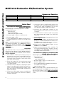
Reference Voltage
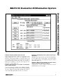
The evaluation software assumes a 2.500V reference
voltage, unless otherwise specified. To override this
value, go to the Measurement tab and type the new
reference voltage next to REF voltage.
Software Listing
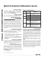
Table 1. Jumper Functions
JUMPER
JU1
The EV kit software disk contains the driver source and
header file. Refer to DRV1416.cpp and DRV1416.h.
Detailed Description
of Hardware
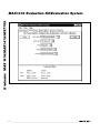
The MAX1416 (U1) is a multichannel, 16-bit, sigmadelta data-acquisition system. Resistors R1–R4 and
C1–C4 act as anti-aliasing filters. The MAX873 (U2) is a
2.5V reference. C14 ensures the MAX873’s stability for
arbitrary values of input capacitor C11. Level translators U3 and U4 allow the kit to support the 3V
MAX1415, as well as the 5V MAX1416. The input signal
can be applied directly to terminal blocks TB2 and TB3.
C5 and C6 bypass the analog-to-digital converter’s
power supply. See Figure 9, and refer to the MAX1416
data sheet.
Evaluating the MAX1415
To evaluate the MAX1415, request a free sample of the
MAX1415EUE and replace U1. Follow the Quick Start
procedure, with the following exceptions:
• In step 1, leave jumpers JU1 and JU2 open.
• In step 3, apply a +3VDC power supply (instead of
+5V) to TB1. Apply an external +1.225VDC differential reference between TB3 pins 3 and 2.
• After step 10, go to the software’s Measurement tab
and type the new reference voltage of 1.225 next to
REF voltage.
Evaluating the MX7705
To evaluate the MX7705, request a free sample of the
MX7705EUE and replace U1. The MX7705 is similar to
the MAX1415/1416 except it does not support internal
clock mode (INT must always be zero).
Using an External Reference
To use an external reference, remove the shunts from
JU1 and JU2, and connect a differential reference
between TB3 pins 3 and 2. The evaluation software
assumes a 2.500V reference voltage, unless otherwise
specified. To override this value, go to the
Measurement tab and type the new reference voltage
next to REF voltage.
SHUNT
POSITION
Closed*
Open
JU2
Closed*
Open
1-2*
Open
JU3
2-3
Closed*
JU4
Open
FUNCTION
U2 (MAX873) supplies REF+
reference voltage
REF+ must be externally connected
REF- connects to ground at U2
REF- must be externally connected
MCLKIN connects to crystal Y1
MCLKIN is not connected
MCLKIN connects to ground
(MAX1416/MAX1415 internaloscillator mode only)
MCLKOUT drives crystal Y1
MCLKOUT is not connected
(MAX1416/MAX1415 internaloscillator mode only)
*Default position.
Troubleshooting
Problem: No output measurement. System seems to
report zero voltage, or fails to make a measurement.
Check VDD supply voltage at TB1. The EV kit requires
a separate supply in addition to the supply on the
microcontroller module. Check the reference voltage
using a digital voltmeter. Use an oscilloscope to verify
that the CS, SCLK, and DIN waveforms are correct. If
the DRDY signal is pulsing, then the software has successfully initialized the MAX1416 and conversions have
been triggered.
Problem: Cannot see MCLK waveform on oscilloscope.
When using an external crystal, the MCLKIN and
MCLKOUT nodes are very sensitive to extra load
capacitance. Connecting a typical 10x scope probe
effectively doubles the load capacitance from 20pF to
40pF, which can slow down or even halt oscillation.
When using the internal oscillator (clock register INT =
1 and CLKDIS = 0), the oscillator signal is visible on the
MCLKOUT pin. In this mode, MCLKOUT can be measured using a typical 10x scope probe.
QSPI is a trademark of Motorola, Inc.
4
_______________________________________________________________________________________