1
13_ELECT.fm
12 ページ
2005年11月18日 金曜日 午後5時40分
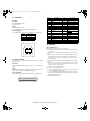
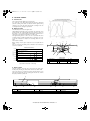
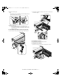
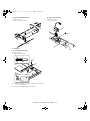
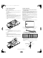
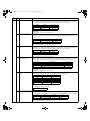
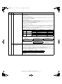
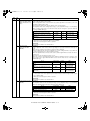
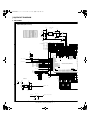
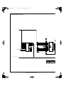
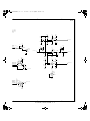
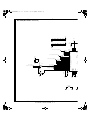
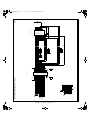
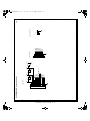
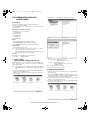
Since the AC power is directly rectified, if there were not this rush current prevention resistor (TH001), an extremely large rush current
would flow due to a charging current flowing through the smoothing
capacitor C006 when turning on the power.
To prevent against this, the rush current prevention resistor TH001 is
provided between the rectifying diode D003 and the smoothing diode
C006, suppressing a rush current.
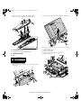
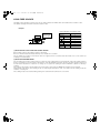
Q001
VDS waveform
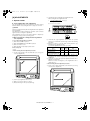
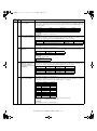
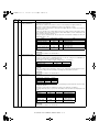
The rectifying/smoothing circuit rectifies a 60Hz AC voltage with the
rectifying circuit, and smoothes it with the smoothing capacitor C006.
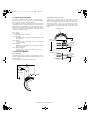
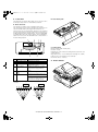
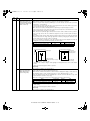
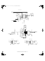
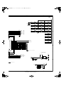
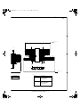
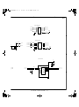
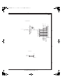
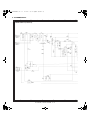
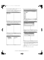
(3) Inverter and control circuit (Ringing choke converter
system)
Q001
ID waveform
ID
Np
Secondary output side
D706 D113
ID waveform
Nc
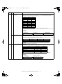
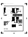
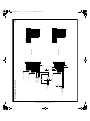
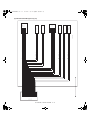
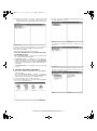
Fig. (5) Ringing choke converter operation waveforms
Ns
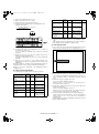
When Q001 turns off, energy accumulated in the transformer (T001)
flows a current of waveform C in the path indicated with dotted line as
shown in the figure above through D101 and D113 and dissipates to
the secondary output side. When this energy is exhausted, the current
flowing through D101 and D113 turns off. However, the NS winding has
a slight remaining energy, which generates a voltage in the base winding NC and turns on Q001 again to repeat switching operation, supplying a high frequency power to the secondary side.
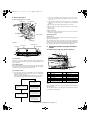
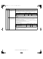
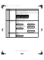
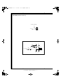
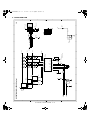
(4) Overcurrent protection circuit (Primary side)
The ON period extension due to an increased output load is detected,
and the OFF period of Q001 is extended by the control circuit, and
energy accumulated in the primary winding of the transformer T001 is
reduced, providing protection against an overcurrent. Refer to Fig. (4).
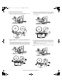
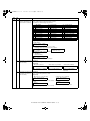
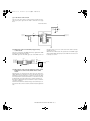
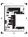
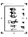
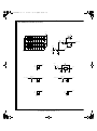
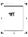
(5) Rectifying/smoothing circuit (+5V)
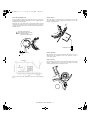
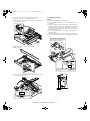
Fig. (4) Inverter and control circuit
When the power is supplied to this circuit, the DC voltage, Vref, supplied by the rectifying/smoothing circuit is applied through R006 and
R007 to FET (Q001), turning on Q001.
When Q001 is turned on, the drain current, ID, flows as the waveform B
in Fig. (5) to apply VDC to the main winding, NP, on the primary side.
At the same time, a voltage is generated in NC winding and applied
through R005 and C008b to the gate of Q001. As a result, Q001 is
turned on rapidly.
At the same time with this, C009 is charged through D001, R001, and
D012. When the potential of C009 reaches 0.7V (= VBE of Q002), Q002
turns on to turn off Q001.
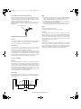
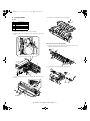
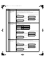
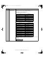
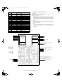
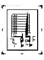
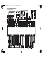
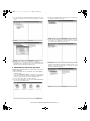
fig (6) Rectifying/smoothing circuit
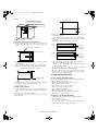
The high frequency pulse generated by the inverter circuit is
decreased by the converter transformer, rectified by the high frequency
diode D113, and smoothed by C107 and C108.
Voltage waveform
Voltage waveform
fig (7) +5V rectifying/smoothing circuit voltage waveform
AR-168N/168L ELECTRICAL SECTION 13 - 12