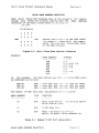
1
ADVANCED DIGITAL
MOLTI SlAVE
Product Reference Manual
ADVANCED DIGITAL CORPORATION
USA OFFICE
UNITED KINGDOM OFFICE
5432 PRODUCTION DRIVE
HUNTINGTON BEACH. CA 92649
TELEPHONE: (714) 891...004
TELEX: 183210 ADVANCED HTBH
27 PRINCESS STREET
HANOVER SQUARE. LONDON W1 R8NQ
UNITED KINGDOM
409-0077 / 409-3351
TLX 265840 FINEST
MULTI SLAVE PRODUCT REFERENCE MANUAL
Revision A.O
Advanced Digital Corporation
5432 Production Drive
Huntington Beach, Cali£ornia
92649 USA
Telephone: (714) 891-4004
Telex:
183210 ADVANCED HTBH
Advanced Digitsl (U.K.> Ltd.
27 Princess Street
Hanover· Square
London, U.K.
(01) 409-0077
Copyright (C) 1985 by
Advanced Digital Corporation
5432 Production Drive
Huntington Beach, Cali£ornia 92649
All rights reserved.
No part o£ this publication may be reproduced,
transmitted,
stored in a retrieval system, or translated
into any language or computer language,
in any £ora or by any
means,
electronic,
mechanical,
magnetic, optical, che~ical,
Dsnual, or otherwise, without the prior written perMission o£
Advanced Digital Corporation.
NOTICES
Page i
Multi Slave Product Reference Manual
CONTENTS
NOTICES
TABLE OF CONTENTS
ii
SECTION I
1-1
i
Introduction •••••••••••••••••••••••••••••••••••••• 1-1
Unpacking/Packing Instructions ••••••••••••••••.••• 1-1
Installation •••••••••••••••••••••••••••.•••••••••• 1-1
Warranty and Return Procedure ••••••••••••••••••••• 1-2
Features end Options •••••••••••••••••••••••••••••• 1-3
Functional Flow ••••••••••••••••••••••••.•••••••••• 1-4
Multi Slave Product Speci£ication •••••••••.••.•••• 1-5
Factory Con£iguration •••••••••••••••••••••••••.••• 1-6
General Notes •••••••••.••••.•••••••••.••.••••••••• 1-7
SECTION II
2-1
Power On/Reset Eventa ••••••••••••••••••.•.•••••••• 2-5
PROM Selection Jumpers .••••••••.••.••••••.•••••••• 2-6
Interrupt Selection Jumpera ••••••••••••••••••••••. 2-6
Slave Sase Address Selection •••.••.••••.•••••••.•• 2-7
Slave Status Port De£initions •••••.••••••••••••••• 2-8
MasterlSlave Communications •••••••.••••.•••••••••• 2-9
110 Address Map ••••.••.•.•••••.•••.•••.•••••••.••• 2-10
Bank and PROM Select Port ••••.••••.••••.••••.••••• 2-11
Serial 110 Controller •••••••••••.••••.•.•••••.•••• 2-12
Counter/Timer Circuit •...••••..•••.•.•..•••••..•.• 2-13
SECTION III
3-1
Fault Isolation and Troubleshooting •...•....•..•.. 3-1
SECTION IV
4-1
Multi Slaye Monitor •..•••.•.•...•..••...•..•...... 4-1
APPENDIX
APPENDIX
APPENDIX
APPENDIX
APPENDIX
APPENDIX
APPENDIX
APPENDIX
A
B
C
D
E
F
G
-
S-100 Bus Pinout •••..•..•...•••.•...••...• A-1
Multi Slave Jumper Options ••...•.•..•..•.. B-l
I/O Connector Pinouts ••..•••.......••..... C-1
110 Port Assignments .•••.•••.•....•.•...•• D-l
Multi Slave Schematic ••.•••....•...•...•.• E-l
Multi Slave Parts List •.•.•..•...••..•.••. F-l
- PS/NET Serial Inter£ace Adaptor .....••.... G-1
H - Signetics 2681 DUART Data Sheet ..•.••••.•. H-l
TABLE OF CONTENTS
Page
ii
Multi Slave Product Reference Manual
Illustrations:
Figure 1-1
Figure 1-2
Multi Slave Block Diagrsn •••••.••.••••..•• 1-4
Multi Slave Component Layout •••••••••••.•• 1-6
2-1
2-2
2-3
2-4
2-5
2-6
PROM Selection Ju.per.s ..••.•••..•..••••.•. 2-2
Interrupt Jumper Selection ••••..••••••.••. 2-2
Base Address Selection .••••••••••••.••.••• 2-3
Master Status Port De£initions .••••••••••• 2-4
Slave Status Port De£initions •.
2-4
Bank and PROM Select Port .••••.••••••••••• 2-7
Figure
Figure
Figure
Figure
Figure
Figure
a
••••••••••
Tables:
T8ble
Table
T8ble
Table
2-1
2-2
2-3
2-4
Master 5-100 Port Assignments •.•.•••.••••• 2-3
1/0 Port Assignments •••..•••••..••••.••••• 2-6
Bank Select Bit De£initions •••.••••••••••• 2-7
Serial 110 Cable Connector •••••••••••••••• 2-8
TABLE OF CONTENTS
Page
iii
SECTION I
Multi Slave Product Reference Manual
Section 1
INTRODUCTION
This Product Re£erence Manual provides information
to install,
utilize and maintain the Advanced Digital Corp.'s Multi Slave S100 bus compatible computer.
The Multi Slave is a single printed
circuit board,
conforming to the IEEE-696 form factor
of 5.25
inches by 10 inches (13.33 cm by 25.4 cm),
providing three independent 8 MHz 280 central processors,
each with two 64k byte
banks of memory, two serial 110 ports, and a counter/tiger.
UNPACKING/PACKING INSTRUCTIONS
When the Multi Slave is delivered by a transfer co~pany,
i t must
be carefully inspected for damage.
Prior to accepting delivery,
carefully inspect the shipping container for obvious damage.
If
damage
is evident,
note i t on the waybill and reqUire that
the
delivery agent sign the waybill.
Notify the transfer company
immediately, and submit a damage report to the carrier.
Remove the Multi Slave and any accessory items from the shipping
container.
Retain
the shipping container any packing material
for
possible reshipment.
Leave the Multi Slave in
its antistatic envelope until installation time.
INSTALLATION
After verifying that the intended enclosure for the Multi
Slave
will provide adequate power and air flow,
remove the Multi Slave
from
its anti-static envelope.
Inspect and
verify
that
the
configuration
Jumpers on
the Multi Slave are correct for
the
Multi
Slave's intended utilization.
Attach I/O cables to
the
connectors provided for serial 1/0 dS required.
Insert the Multi
Slave printed circuit board into a Buitable 5-100 bus slot connector.
INTRODUCTION/UNPACKING/INSTALLATION
Page 1-1
Multi Slave Product Reference Manual
Section 1
WARRANTY AND WARRANTY RETURN PROCEDURE
Advanced Digital Corporation warrants that its products will
be
£ree from defects in material and workaanship £or a period of 360
days of shipment from the factory.
1£ a
customer experiences a defect in either workManship or
materials during the warranty period,
noti£y your supplier i.mediately.
Your supplier may repair the Multi Slave or deter.ine
if some other action is'to be taken.
In the event that a return
o£ the Multi Slave is deemed neccessary, obtain a RETURN MATERIAL
AUTHORIZATION (RMA) NUMBER from your supplier.
Repack the Multi Slave and any accessory iteas in the original
packing material and ship i t in accordance with your supplier's
shipping instructions.
Make sure the RMA number
is clearly
marked on the shipping label.
Your supplier will
not accept
delivery of a return shipment without the proper RMA number.
**********************.
WAR N I N G
*
*
**********************.
The Multi Slave as delivered does not generate,
use,
or radiate
radio frequency energy.
However, after installation and application of power,
the Multi Slave may generate,
use,
or radiate
radio frequency energy.
Advanced Digital Corporation recoMaends
that the Multi Slave be installed in an enclosure which complies
with the provisions for computing devices pursuant to Subpart J
of Part 15 o£ FCC rules, which are designed to provide reasonable
protection against such interference.
WARRANTY
Page 1-2
Multi Slave Product Reference Manual
Section 1
FEATURES AND OPTIONS
The Hulti Slave provides the following features:
a
Three
independent a-bit, a MHz
a
Each CPU has 128k of memory,
configured as two 64k
byte banks, with a 1k to 16k area of co~~on (shared)
memory.
a
Two asynchronous serial 110 ports per CPU.
Level
conversion to EIA RS-232C or RS-422 standards i&
provided via the PS/NET (paddle card) accessory.
o
Independent baud
o
Counter/TiBer
o
User selectable PROM, Jumper configurable for one o£
the following: 2716, 2732, 2764, 27128, or 27256.
o
I££E-696 5-100 Bus Compatibility
o
Auto.atic power-on/reset bootstrap loader and resident monitor/debugger utility.
FEATURES AND OPTIONS
280 Microprocessors
rate selection on each serial port
providing real tiBe clock
capability
Page 1-3
Multi Sleve Product Reference Manual
Section 1
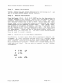
.....
....
~
..
po'
rt
..
....
~
~
..
.--+
A
+2681
DUARl
----.
f4-
-fJ
r--
...
...
....
.
...
PROM
.1
Z80-H
CPU
(1 of 3)
.
~
>---
....
r-----.
...
Bank
64k
RAM
Control
& Timing
'--
p,r ~
L_---..
.. I NTER-
FACE
....
S-100
BUS
"-
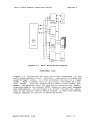
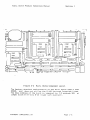
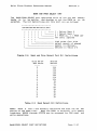
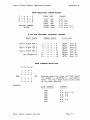
Figura 1-1
Mult! Slave Block D1agraa
FUNCTIONAL FLOW
Figure 1-1
illustrates the maJor £unctionsl components of
the
Multi Slave computer board.
Initially. immediately following the
power-on/reset event,
all three processors are held in a
reset
state.
Each
processor must be individually activated by e network
master.
Once t.he master has activated a Multi Slave processor~ the selected slave CPU then begins executing the instructions provided by the onboard EPROM. Depending upon user response
and intervention,
the proceenor will either initiate the
execution of the resident Monitor/Debug program, or begin the download
request sequence to receive an operating system.
MAJOR FUNCTIONAL FLOW
Page 1-4
Multi Slave Product Re£erence Manual
Section 1
HULTI SLAVE PRODUCT SPECIFICATIOH
Physical and Environmental:
For. Factor
IEEE-696 S-100 standard
5.25 inches x 10.0 inches x .75 inchea
Size
Weight
14 oz.
Temperature
operating
storage
·0 to 50 degrees Ce1c1us
-65 to 150 degrees Celciua
Humidity
o to
Altitude
o to 10,000 £eet (operating)
95~,
non-condensing
Power Requrements:
+5VDC @ xx.x Amps (xx Watts)
Power Regulation
On board, providing 4.75 to 5.25VDC
Cooling
1-5 CFH <cubic £eet per
~inute)
air £1ow
Power Supply Requirements:
Unregulated
+ 7VDC Hin1JluJl
+11VDC Average
+25VDC HaximuD <peak)
+14.5VDC Minimum
+21.5VDC Average
+35.0VDC Maximum (peak)
-14.5VDC Minimum
-21.5VDC Average
-35.0VDC Maximum <peak)
Functional Speci£ication:
Processor
2i10g 280H
Memory
128k Dynamic RAM
Processor Clock
8.000 MHz
Serial Controller
Signe~ics
FACTORY CONFIGURATION
2681 DUART
Page 1-5
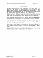
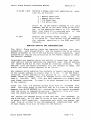
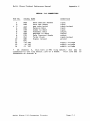
Hulti Slave Product Re£erence Manual
Figure 2-2
Section !
Multi Slave COMpOnGnt Layout
The £actory standard con£iguration o£ the MuJti Slave uses a 2764
EPROM,
end
does not utili.ze the 5-100 Vectored Interrupt Lines.
The base address of the board is Jumpered £01 110 address 90H
at
Jumper block E-19 thru E-26 (lower left quadrant).
FACTORY
CONFIGURAT~ON
Page 1-6
Multi Slave Product Reference Hanual
Section 1
GENERAL NOTES
The Multi Slave contains three independent 2i109 280-H CPUs.
The
principal 110 device £or each processor is the Signetics 2681
DUART
<Dual Universal Asynchronous Receiver/Transaitter).
This
particular device was cnosen £or its many i'eatures, which include
an internal duel baud rate generator and counter/tiaer.
Several types of PROMs are supported by the Hulti Slave, based on
Jumper options.
The PROM types supported are a8 %ollowa:
2716,
2732, 2764, 27128 ~nd 27256.
PROM addressing begins at OOOOH.
Each processor contains a total 0% 128k o£ user available .eMory,
configured as two 64k banks, and is selectable through ao£tware.
There is only one interrupt source on the Multi Slave,
which i8
provided by the DUART.
Typically,
the 280 CPU will be operated
using Mode 1 interrupts (see the 2ilog ZBO Technical Hanual £or a
discussion o£ 280 interrupt modes>.
Each slave is also capable o£ interrupting the master via the S100 vectored interrupt lines.
This will be discussed in detail
later.
Each 280 CPU is driven by a cent!al 8 MHz oscillator;
DUARTs are driven by a COMmon 3.6864 MHz crystal.
GENERAL NOTES
the
Page 1-7
three
SECTION II
Multi Slave Product Re£erence Manual
Section 2
POWER-ON/RESET EVENTS
Each Multi Slave CPU is held in a reset state until such ti.e 8S
the master enables the operation o£ a slave.
The master enables
a
slave by issuing an output byte to the slave's base address
with bit D4 reset.
The PROM is automatically selected,
and
instruction execution begins at address OOOOH.
The
ADe supplied PROM initializes
bo~h channels o£ the DUART
to
then tests channel A £or an available input character.
I£ a character is available, the Multi Slave monitor is activated
which issues the £ollowing message to the terMinal on channel A:
9600 baud,
Multi Slave Monitor Version 1.x Generated HM-DD-YY
Copyright ee) 1985 Advanced Digital Corporation
Enter
~?~
£or HELP
A complete discussion o£ the Multi Slave
section IV o£ this manual.
~onitor
~ay
be £ound in
1£ an input character is not available at serial chennel A within
approximately 100 milliseconds,
the startup program will
enter
the cold boot process,
sending an operating system download
request to the master processor over the S-100 bus.
POWER-ON/RESET EVENTS
Page 2-J
Multi Sleve Product Re£erence Manuel
Section 2
PROK SELECTION JUMPERS
Each CPU has a Jumper block to select the PROM
£ollowing table to set these Jumpers.
E. ,-& S4-IIP ez.'7_?lf
1
0
0
3
0
0
5
7
0
0
2
4
6
0
0
8
PROM TYPE
TYPICAL JUMPER
BLOCK
Figure 2-1
Usa
the
JUMPER
--------(2K)
2716
2732
2764
27128
27256
type.
------
3-5,
5-7,
1-3,
1-3,
1-2,
(4K)
(8K)
(16K)
(32K)
4-6
4-6
5-7
6-8, 5-7
6-8, 5-7
Hulti Slave PROM Selection Ju.pera
INTERRUPT SELECTION JUMPERS
Each Multi Slave CPU may interrupt the master processor on one of
two 5-100 vectored interrupt lines.
Selection o£ interrupts 1.
8S £ollows:
JUMPER BLOCK
MULTI SLAVE
-----------
.. ..
Multi Slave CPU 0
II
II
.
..
Multi Slave CPU 1
••
••
CPU
Slave
2
M.ulti
II
II
II
No
••
.
..
Connection
Figure 2-2
5-100 BUS
-----------J7
1
---------
3
0
0
5
0
0
7
9
0
0
0
0
2
4
6
8
10
11
13
0
0
12
0
0
15
0
0
14
16
0
0
INTOINT1INT2INT3INT4INTSINT6·
INT7-
(pin
(pin
(pin
<pin
(pin
(pin
(pin
(pin
4)
5)
6)
7)
8)
9)
10)
11)
Kulti Slave Interrupt 3uaper Selection
I£ the interrupt selection structure shown above is not suitable.,
wire wrap connections between the Ju.per block pins .8Y be used
in place o£ Jumper plugs r thus allowing any given Multi Slave CPU
to use any 0% the eight 5-100 vectored interrupt linea.
PROM/INTERRUPT SELECTION JUMPERS
Page 2-2
Multi Slave Product Reference Manual
Section 2
SLAVE BASE ADDRESS SELECTIOW
Each Multi Slave CPU occupies :four o£ the r.aeterls
I/O ports,
though only three are actually used by each CPU.
Base address
selection o:f the Multi Slave board is as £ollc;ovs:
t=J~- E'l.~
(7)(6)(5)(4)
1
3
5
7
a
0
0
0
a
0
a
a
4
I
6
8
AddreSB selection Ufas LOW TRUE LOGIC
Cno Jumper=l, Jumpcled=O)
and represents the four ~oBL signi£icant bita
of the base address.
LSB
MSB
I
2
I
Figure 2-3
Hulti Slav. Baaa
Selection
Add~Od~
Example:
BASE ADDRESS
JUMPERS
- _._---
------------
"
'JOH
80H
90H
AOH
1··2
3-4, 5-6,
3· 4, 5-6
8'''4, 7-8
BOH
IE,
£or example,
3 ··4
"0,.
COH
~~~
DOH
::.~
7-8
7-8
(:
-.J
the base addresR waR BOIl, Lhe three CPUs would
be addressed as £ollowa:
BOH
CPU #0
CPU #1
CPU #2
The master
<5-100)
;
88H
;
not used)
on:::;
," :2H
~83H
uses 84H, 85H, nn(,j
usee BAH, B9H, 8.na
B6H
<87H not used)
cBSH not used)
uses 80H,
84H
81H.
f.~AH
data port assignments ere r.11., i 0110'..,.5:
TYPE
FUNCTION
+0
R/W
Read Sl~ve St~tus
Write Control bits
+1
R/W
5-100 Datt! Port.
+2
R/W
Read = De-assert ALIVE- bit
Write= De-sesert SLAVE MESSAGE bit
BASE ADDRESS
Table 2-1
i~ee
d~tails
Haater 5-100 Port AaaigJ1M\snta
SLAVE BASE ADDRESS SELECTION
Page
2·- 3
below)
Multi Slave Product Reference Manual
Section 2
SLAVE STATUS PORT (read by Master Processor
.--.--.--+--.--+--.--.--+
1071061051041031021011001
.--+--+--+--+--+--+--+--+
1
1
= MASTER MESSAGE set
= SLAVE MESSAGE set
o =
o
o =
1 =
o =
ALIVEw bit set
Slave i s in HOLD.
Slave i s WRITING 5-100 data
Slave 1s REAOING S-100 data
Slave RESETw active
STATUS PORT (written by Haster Processor)
+--+--+--+--+--+--+--+--+
1071061D5104J03102101JOOJ
+--+--+--+--+--+--+--+--.
1
1
Figure 2-4
=
=
set MASTER MESSAGE bit
reset slave processor
Haater Statu. Port Bit Oa£intiona
Note that bits 06 and D7 of the STATUS PORT are not used, and are
on (1) when the port is read by the Master Processor.
Note also
that there are four low active terms;
ALIVE., HOLD~, WRITE*, and
RESET-.
SLAVE STATUS PORT BIT DEFINIT10NS
Page 2-q
Multi Slave Product Re£erence Manual
MASTER/SLAVE
'::;ect. i OTl
:z
COM~UNICAT!ONS
For the master processor to send data to the
slRve,
the
sl~v~
must be reading the 5-100 data port.
Conversly, £or the slave to
send data to the master,
the slave must write to the 5-100 data
port be£ore the master reads it.
As mentioned ea1'li~r, when the
slave is reading or writing to the S-100 data port,
it is placed
in
8 HOLD (wait) condition,
and released to resume
processing
when the Master Processor writes or reads the corresponding port.
This ensures that the master and slave(s) remain in synchronization during
bus communication;
reliable network
operation
1s
achieved
when the other status bits
(ALIVE-,
READ/WRITE-,
and
HOLD-) are implemented as part o£ a communications protocol.
The Haster Processor may reset a slave processor at any time
by
issuing an output to the appropriate slave status port with
bit
D4 set.
To reactivate the slave, the master must again issue an
output byte to the slave's status port with bit D4
reset,
£01lowed by a short post-reset delay.
An e~arnple of this
sequence
is shown below:
SL_RES:
SL_R05:
SL_R10:
A,lOH
(SLVBASE),A
B,,16
SL R05
NOT 10H
(SLVBASE),A
B,16
(SP),HL
EX
(SP),HL
EX
DJNZ SL R10
RET
LD
OUT
LD
DJNZ
)COR
OUT
LD
;
;
;
.;
,
;
;
;
;
SET BIT D4
OUTPUT TO SLAVE BASE ADDRESS
LEAVE THE BIT SET
FOR A SHORT TIME
TURN OFF BIT D4
UN-RESET THE SLAVE
SET UP FOR POST-RESET DELAY
THIS IS A
VERY EFFECTIVE
TIME WASTER
RETURN TO CALLER
...
...
The suggested
handshake mechanism between the master and
slave
is as £ollows (£or transmission £rom slave to master):
the slave
first asserts the SLAVE MESSAGE bit.
The master t,ay see this by
polling
(reading the slave status pbrt),
or the Multi Slave may
be configured to cause an interrupt on the
master.
In either
case, once the SLAVE MESSAGE bit has been asserted, the slave CPU
then outputs its £irst data byte to the S-100 bus communications
port.
Upon doing so, the slave CPU is £orced into a wait condition,
which
the
master must veri£y by testing the
WRITEand
HOLD~ bits at the slave status port.
Once the master has determined
that
both signals are true,
i t may then
read
the
byte
waiting at the S-100 data port.
The elave is rel~ased to resume
processing,
£ree to continue sending subsequent data bytes, etc.
master to slave transmission,
the master must SBsert
th8
In
a
which the slave sees by polling i t s '
status
port.
MASTER bit,
detecting
the active MASTER bit,
the elave must reset
it
Upon
MASTER/SLAVE COMMUNICATIONS
.o age
'"' - c;
_
.~
Multi Slave Product Re£erence Manual
Section 2
(indicating to the master that the slave is ready to accept the
message),
and
immediately issue a read to the 5-100 data port.
Again, the slave processor is £orced into a wait condition. which
the aaster must veri£y by testing the READ and HOLD- bits at the
slave status port.
Once the master has determined that both signals are active,
i t Day then write the data byte to the 5-100
data port.
The slave is released to resume processing,
£ree to
continue receiving subsequent data bytes, etc.
The £ollowing page provides a brie£ example o£ this
dialogue:
MASTER/SLAVE COMMUNICATIONS
master/slave
Page 2-6
Multi Slave Product Re£erence Manual
Section 2
MASTER PROCESSOR (RECEIVING MESSAGE FROM SLAVE)
IN
BIT
RET
OUT
WAIT1:
IN
BIT
JR
BIT
JR
IN
RET
A, (SLVSTAT)
SLVMSG,A
NZ
(MSGRST),A
; GET SLAVE STATUS
; IS SLAVE MESSAGE BIT SET?
; NO, RESUME OTHER TASKS (ACTIVE LOW)
OUTPUT CLEARS SLAVE MESSAGE BIT
; (CONTENTS OF A-REG INSIGNIFICANT)
A, (SLVSTAT)
SLVWRT,A
NZ,WAITl
SLVHLD,A
NZ,WAITl
A, (SLVDATA)
GET SLAVE STATUS BITS
IS SLAVE WRITING TO 5-100 PORT?
LOOP IF NOT
; IS SLAVE IN A HOLD CONDITION?
LOOP IF NOT
; ALL IS READY - GET THE DATA BYTE
; AND RETURN TO CA~LING TASK
MASTER PROCESSOR (SENDING MESSAGE TO SLAVE>
LD
OUT
WAIT2:
IN
BIT
JR
WAIT3:
IN
BIT
JR
BIT
JR
LD
OUT
RET
A,OOOOOOlOB
(SLVSTAT),A
SET MASTER MESSAGE BIT ...
••. SO THE SLAVE WILL SEE IT
A, (SLVSTAT)
MASTER,A
NZ,WAIT2
GET SLAVE STATUS
HAS THE SLAVE RESET IT YET?
LOOP UNTIL HE HAS DONE SO
A, (SLVSTAT)
SLVWRT,A
Z,WAIT3
SLVHLD,A
NZ,WAIT3
A,(HL)
(SLVDATA),A
GET SLAVE STATUS AGAIN
IS SLAVE READING THE 5-100 PORT?
LOOP IF NOT
IS SLAVE IN A HOLD CONDITION?
; LOOP IF NOT
GET BYTE TO SEND
SEND IT TO THE SLAVE
AND RETURN TO CALLING TASK
SLAVE PROCESSOR (RECEIVING MESSAGE FROM MASTER)
IN
IN
RET
A, (HASTER)
A, (DATAPORT)
; CLEAR MASTER MESSAGE BIT
AND IMMEDIATELY READ THE S-100 PORT
; RETURN TO CALLING TASK
SLAVE PROCESSOR (SENDING MESSAGE TO MASTER)
IN
LD
OUT
RET
A, (SLVMSG)
A,B
(DATAPORT),A
; SET SLAVE MESSAGE BIT
B-REG HAS DATA BYTE TO SEND
; OUTPUT DATA BYTE TO 5-100 DATA PORT
; RETURN TO CALLING TASK
Note that these examples transmit and receive only a single byte
at a
ti~e and provide only a skeletal communications
protocol.
The slave may utilize the 280 block input and output instructiona
to receive and trana~it any number o£ bytes to the master, though
the user
should employ a slightly more sophisticated protocol
when doing so.
In typical networking environments,
the £iret
byte transmitted contains the length o£ the message
to £ollow,
Implementation of such networking schemes i8 leit to the user.
MASTER/SLAVE COMMUNICATIONS
Page 2-7
Multi Slave Product Re£erence Manual
Section 2
BOOTSTRAP SOFTWARE
The £ollowing program will provide the user with a
bootstrap
£8cility which £ollows the protocol set £orth in the prior section.
This program is identical to that contained in the Multi
Slave monitor PROM r
and assumes that an intermediate loader will
be received £rom the master.
SLVMSG
SALIVE
SDATA
SHl1EH
EQU
EQU
EQU
EQU
20H
60H
0070H
BOOOH
;
110 READ SETS SLAVE MESSAGE BIT
110 READ SETS SLAVE ALIVE BIT
; B=HESSAGE LENGTH r C=PORT ADDRESS
; ONLY ADDRESSES ABOVE BOOOH ARE
; ACCESSABLE WHILE PROM IS ENABLED
BOOT:
IN
IN
LD
Ar(SLVMSG)
Ar (SALIVE)
BCrSDATA
OUT
LD
(C) rB
HLrSHMEM
INIR
JP
SHHEM
SET SLAVE MESSAGE BIT
SET SLAVE ALIVE BIT
B=BYTE COUNT (0=256 BYTES)
C=PORT ADDRESS
SEND BYTE COUNT FIRST
; ADDRESS TO STORE INCOMING MESSAGE
(WHICH WILL BE THE INTERMEDIATE
; LOADER PROGRAM)
RECEIVE ENTIRE MESSAGE FROM MASTER
BRANCH & EXECUTE INTERMEDIATE LOADER
;
;
;
;
MASTER/SLAVE COMMUNICATIONS
Page 2-8
Multi Slave Product Re£erence Manual
Section 2
110 ADDRESS HAP
Each Multi Slave CPU has an identical I/O address map.
assignDents are as £ollowa:
ADDRESS (Hex)
OO-OF
The port
TYPE
FUNCTION
R/W
DUART Data/Control (see Signetics
2681 Docu~entation £or details)
Not Used
10-lF
20-2F
R
Asserts SLAVE MESSAGE bit
30-3F
R
De-asserts MASTER MESSAGE bit
40-4F
w
BANK/PROM SELECT (details £ollow)
50-SF
R
STATUS PORT (MASTER and SLAVE bits)
60-6F
R
Asserts SLAVE ALIVER bit
70-7F
R/W
S-100 DATA PORT
Table 2-2
110 Port Aaaignaonta
The user should be aware that although it would appear that the
5-100 data ports would collide with one another, they are actually physically separated in the hardware.
This is explained a bit
more clearly by the £ollowing diagram:
SLAVE PROCESSOR NUMBER
#0
#1
#2
MASTER PROCESSOR
I/O ADDRESS 70H •••.••••••••.••.•..• I/0 BASE ADDRESS
+
0
1/0 ADDRESS 70H ••••••••••••.••..••• I/0 BASE ADDRESS
1/0 ADDRESS 70H •••••••••••••••••••• I/0 BASE ADDRESS
+
4
8
+
SLAVE STATUS PORT (read by the Slave, read only>
+--+--+--+--+--+--+--+--+
1071061051041D31021011001
+--+--+--+--+--+--+--+--+
1----- 1
--------- 1
Figure 2-5
SLAVE 1/0 ADDRESS MAP
= MASTER message active
= SLAVE message active
SlavQ Status Port Bit Definitions
Page 2-9
Multi Slave Product Ref'erence Manual"
Section 2
BANK AND PROM SELECT PORT
The BANK/PROM SELECT port apeci£iea which of' the two 64k
memory
banks is to be active,
and whether or not the PROM is
to
be
selected.
The bit de£initions £or this port ere as f'ollows:
?--?--?--?--?--?--?--?--+
1071061051041031021011001
=
Select Bank 0
Select Bank 1
o = PROM on, 1 = PROM o££
not used, ignored
1
1
=
high order four bits
select amount o£ shared
memory (in Kbytes),
de£ined in Table 2-3
Figure 2-6
Bank and Prom Seloct Port Bit
Bits D4-07
Hex Value
----0
1
2
3
4
5
6
7
8
Table 2-3
D~£inition.
Shared
Amount
-----16k
15k
14k
13k
12k
11k
10k
9k
8lt
7k
9
A
B
6k
5k
C
4k
D
3k
E
F
2k
lk
Bank Select Bit De£initionA
NOTE: Bank 0 and 1 are mutually exclusive and must not be set
active at the same time.
When the PROM is selected, only memory
locations BOOOH through OFFFFH may be accessed £or RAM read
and
write operations.
BANK/PROM SELECT PORT OEFINTIONS
Page 2-10
Multi SIeve Product Reference Menuel
Section 2
SERIAL 1/0 CONTROLLER
The Multi SIeve provides two independent aerial IIO channels per
CPU,
both contained in one seriel 1/0 controller, tho Signetica
2681 Dual Aaynchronoua Receiver/Transmitter (DUART).
The DUART
containa two internal,
independent baud rate generators, capable
o£ producing 18 user selectable baud rates.
Level conversion to
EIA RS-232 or RS-422 level is provided by an external circuit
aa ••• bly called the PS-NET.
SERIAL CHANNEL CONNECTORS
Connectors for each serial liD channel are located aerOS8 the top
o£ the Multi Slave board (see figure 1-1 £or exact place.ent).
Each connector has the following pinout:
PIN NO.
------1
2
•
3
4
3
6
7
8
9
10
11
12
DIRECTION
SIGNAL NAME
----------Data
Carrior Detect
Data Set Ready
see note below
Receive Data
Clear to Send
Transtlit Data
Request to Send
Data Terminal Ready
Tx/Rx Clock
Signal Ground
DCD
DSR
•••
RXD
CTS
TXD
RTS
DTR
CLK
GND
N1C
+16 VDC
13
-16 VDC
14
+5
VDC
---------
input
input
input/output
input
input
output
output
output
input/output
ground
supply voltage
supply voltage
supply voltage
•
On channel A,
this term is RNG (ring detect)
and may
connected to the ring detect line on a Dodea.
This line has
connected on channel B.
Tabla 2-4
SERIAL IIO CONTROLLER
Serial 110 Cable Connector
Page 2-11
be
no
Multi Slave Product Re£erence Manual
Section 2
COUNTER/TIMER CIRCUIT
The counter/timer circuit is contained on the DUART device.
As
its name implies,
i t may be used as a timer (programmable divider) or a counter,
providing an appropriate indication when
the
specified countdown value has reached zero.
It should be noted that unlike the 280 eTC, the DUART's counter/timer
uses a 15-bit countdown register,
providing much greater
£lexibility in its application.
Appendix H contains the data sheet £or the Signetics 2681 device.
2581 DUART Specifications
Poge 2-12
SECTION III
Hulti Slave Product Re£erence Manual
Section 3
FAULT ISOLATION
Fault
isolation
is the process o£ identifying a fault
and
the
resultant cause of the £ault to the lowest possible level.
This
section deals with hardware fault isolation and
is generally
independent o£ so£tware considerations.
Prior to any attempt at fault isolation,
a test environment must
be validated.
Generally, the test environment. will consist o£ an
5-100 chassis,
motherboard,
power supply,
S-100 extender card,
snd
a known good Multi Slave.
Validation consists o£
removing
all
other 5-100 circuit cards from the chaSSiS,
and
any
other
devices loading the +8, +16, and/or -16 VDC power supplies.
Having
removed all circuit boards from the
motherboard,
verify
that
the £ollowing voltages referenced to ground (5-100 bus
pin
50 and 100) are within the tolerances listed below:
DEFINITION
S-100 PIN
---------
----------
+ 8
+ 8
+16
-16
1
51
2
52
VDC
VDC
VDC
VDC
MINIMUM
AVERAGE
MAXIMUM
-------
-------
-------
+7.0
... 7.0
+14.5
-35.0
+11 .0
+25.0
... 25.0
+35.0
-14.5
"'11.0
+21.5
-21.5
The above conditions must be met before proceeding with the next
teat..
Step 1:
Visual
V~rificdtion
Inspect the suspect Multi Slave to verify that
components are
correctly
installed and properly seated in their sockets.
Components may be compared against a known good Multi
Slave.
All
DIP components have t.he Bame pin 1 orient.ation.
Step 2:
On Board +5 VDC Regulation
Remove
power from the
card
into
a suitable
Multi
Slave
into the
measure the voltage at
and 5.25 VDC.
Step 3:
Clock
motherboard.
Insert the S-100 extender
slat in the motherboard,
then insert
the
extender card
Bocket.
Apply
power
and
Ul-16.
This voltage must be between 4.75
Veri£jcat~an
Veri£y the clock £requenciea at the £ollow1ng locations:
U57-7
80ns
U49-8
150ns
FAULT ISOLATION
central clock distr~buted to all
CPU"s.
central SIO clock distr~buted to
all DUART's.
Page 3-1
Multi Slave Product Re£erence Manual
Step 5:
Section 3
Memory Veri£ication
Veri£y
memory row and column addressing by monitoring pin 1
pin 19 on each AM2965 memory driver circuit.
Step 6:
and
Monitor Veri£ication
Data Set Ready (Jl-2,
J3-2, J5-2) MUST be low for the monitor to
issue a message to the console.
Verify that the PS/NET-1 card ie
properly con£igured and connected to the Multi Slave,
and
that
the
terminal's baud rate is set to 9600.
Ensure that the
Mul~i
Slave card
ia in a reset-hold condition by pressing the
system
reset button on the computer's front panel.
Then, using a monitor program on the Master Processor,
activate the desired
slave
CPU by issuing an OUT <slave command port),40H.
The Multi Slave
monitor
should issue its logon message as described in Section 2
of
this manual.
Press any key on the slave console within
two
seconds a:fter "un-resetting" it.
The Multi Slave monitor should
then be ready to accept "::.~("Jmmands.
STEP 7:
Ve r i fit.: d t.i () n
0
f
0
t 1) e
l'
Ma J 0 r
Co mpo n e n t s
Verification
of other maJor Multi Slave components requires
development
of
short software routines which will
provide
scope
Inops to support Lhe analysis of Multi Slave signals some of the
more
commonly
required routines have been incorporated
in
the
Multi Slave Monitor program.
These tests include memory and I/O
.read and wr 1 te loops.
See t.he moni tor command lIst :for
:further
informatiofJ.
o q)(
F.o\ULT ISOLATION
Page
3-2
SECTION IV
Multi Slave Product Reference Manual
Section 4
THE MULTI SLAVE MONITOR
The Multi Slave contains a very powerful monitor program, providing numerous features not found in moat simple monitors.
Some of
the highlights include:
The basic
o
Full %unction decimal/hexadecimal calculator
(expression evaluator)
a
280 disassembler
o
Off"set variable :for LIST and DUMP functions
a
Comprehensive memory
o
Printer echo
(all console input & output may be
echoed to the printer) with user selectable baud
rate
o
Scope loops - memory and 1/0 readlwrite loops
mo~itor
command structure
COMMAND LETTER
[VI
r,V2
(,V3JJJ
diagnoat~ce
15
as follows:
<CR>
where Vl, V2, and V3 are var1ables (command parameters), and
Parameters
unless ~ndicated otherwise,
are hexadec~mal values.
mayor may not be requ~red depending upon the command.
Note that
<CR>,
and
ALL commands are termInated by a
carriage
return
fields wi~hin brackets ( [ l ) are optional.
MONITOR COMMANDS
BOOT
this
slave system by
issuing
an
opsystem download request to the
master.
For
specific details about the
download reques t pr . .)gram,
see "Master /Slave Commun.i.cat lons"
.In sect.~on I I o:f this manual.
B
erat~ng
COMPARE
~he contents o£ memory,
starting at
address Xl to address X2,
£or X3 bytes. If a
mismatch occurs, the contents o:f both addresses will be displayed.
D Xl
[X2JJ
MULTI SLAVE MONITOR
DUMP
the
contents o£
memory
beginning
at
address
OOOOH
<i£ the DUMP command has
not
been previously ~nvaked),
or contInue at the
last address plus one,
or at address Xl
for
256 bytes (or thru address X2).
SEE OFFSET
(S) COMMAND.
Page 4-1
Multi Slave Product Re£erence Manual
Sect~on
F Xl,X2,X3
FILL memory from address Xl
value X3.
G Xl
GO to address Xl (via a CALL) and
instructions at that address.
H
See
the next subsection for details of
command.
4
thru X2 with data
exec~te
the
tholS
I
Xl
INPUT data from I/O port address Xl and d.1splay 1~ on the console.
To display the
contents
of the next sequential port,
enter
a
carriage
return:
to display the contents of
the prlor port, enter a minus (-) sign.
}{
[N1J
D1 st.,} ay
t he cur k
811t
bank
number,
or
swi tch t.o
bauk Nt.
L rx.!
rX2J 1
11 X1,X2,)(3
l.IST,
using 280 mnemonics,
the .lnstructions
beginning
at address OOOOH (i£ the LIST co~
Jnand
has not been
previously
invoked),
or
'_:lJnLinue at t,he last address pluB one,
or at
ddrlr~ss
Xl for 18 lInea of instructione,
or
t.hr u addr c·gS X2.
SEE OFFSET (:$) COMMAND.
MOVE
tta~
dr €.. f.~p..
X:~
contents of memory beginning at adaddr·t,~8E'. X2 to address X3.
t.hl' LJ
a
X1,X2
OUTPUT data byte X2 to I/O port address Xl.
P
(rll)
Toggle the PRINTER online Dr offline,
or set
t tl e p:r 1 n t. ~ r b a \j d 1· a t ~ t LI val u e D 1 ( dec 1 mal ) .
S
Xl
::':;ET the. ~:unt.:~lItR of
•.: ',.:> n t. f?, n t!-!. l) ( t. hem €.- m0
T
LXl
The current
l I be
dis played.
Enter
<CR> to advance to the
next
.a •..1d 1" ~~!? S ,
(-)
tog (l b de k t CJ the p r 1 or address,
t w (.;.
h ~ >= ~ dec i mal
c h a (" a c: t. t? r s
(0 - 9 ,
A- F)
t 0
',:: h:s 1"1 9 02
t h 8 h t::' X val u e ,
(,) 1
( , A)
t 0 c han g e t h e
c·· (:II J t .~ n t ..•. l (.1 A:) C T T val 1I eA.
r,X211
tlddrE-'flB
l'
Y
Xl.
1 0 cat .l 0 n
W1
tJeglllnlng at OOOOH thru the h~gh
address tt.hp- starting address of
-1),
01" st.al· t i ng at add1' eSB
Xl
addret:.t,f'. XL').
A plus sign (-t-) will be
TEST mt:!muty
t~~.t
the
posS.l.ble
mt"Jn L t_Ol·
(tll:l·U
With each Buccess£ul pass.
Any adell-ee,s
'..."hleh fai 18 will be displayed
at
the
console,
along wlth the e~pected and £a.111ng
data
pattern.
Upon
completion of the
test
(one
complete pass at all specli.led
addreeceo),
the test will be termlnated and a message will be d.lBplayed at the coneole.
~isplayed
Page
'1-2
Slave Product Re£erence Manual
~ulti
Z Xl,.X2
(,.X3l
Section 4
Perform a Scope Loop test specified by
tion Xl,. as follows:
o
1
2
3
func-
= Memory Read Loop
=
=
=
Memory Write Loop
110 Read Loop
110 Write Loop
Field
X2 is the memory address or 110 port
address,. and X3 is the data value to be written
to the specified memory or 110 address.
Note
that field X3 is required only
if
the
test function is a write operation.
S
(Xl]
Display the current offset value,
or
change
i t to value Xl.
This offset will be added to
the
address
specified in the DUMP and
LIST
commands.
MONITOR ASPECTS AND CONSIDERATIONS
The Multi
Slave monitor takes two important factors
into consideration;
self preservation,
and the pOssibility of an active
master processor on the 5-100 bus during monitor execution.
Self
preservation implies the protection of the memory region in which
the monitor resides.
Interrupts are enabled while the monitor is executing; the interrupt service routine performs one important tasK, that of setting
the SLAVE ALIVE bit at each 16.666 ms interrupt interval.
This
ensures that the master processor will not attempt to reset
the
slave; the slave always appears to be "alive."
Any command which modifies the contents o£ memory performs a test
of the target address to ensure that it i8 not
1) the 280 Mode 1
interrupt
vector address or any portion of
it
(i.e.
locations
0038H, 0039H or 003AH), and 2) an address within the monitor.
In
case 1,
the SET,.
TEST,
FILL and MOVE commands will simply skip
over these locations.
In case 2, an error message will be issued
to the console.
There are
two
1/0 address groups which muet be
accessed
with
care.
The first group is 20H thru 2FH; an 1/0 read in this range
asserts the SLAVE MESSAGE bit, indicating to the master processor
that the slave is requesting service.
Typically, this will i n i t iate the operating system download sequence.
The second 110 address group is 70H thru 7FH,
the "gateway"
to
the 5-100 bus.
An 1/0 read or write in this range causes the CPU
to enter a WAIT condition,.
terminated only a£ter the master
has
read
from or written to the corresponding
communications port.
In most cases, this will be £atal to the monitor.
MULTI SLAVE MONITOR
Page 4-3
Multi Slave Product Reference Manual
Section 4
To prevent an inadvertent read or write to these ports, the monitor will prompt with:
CONFIRM (YIN):
when
i t encounters a read or write request to anyone of
the
a£orementioned addresses.
A single keystroke reply is required,
either 'y' to perform the requested function, or any other key to
terminate it.
OTHER FEATURES AND FACILITIES
The
Hulti
Slave monitor provides a means of obtaining
hardcopy
output o£ all console 1/0.
When hardcopy
output
is desired,
execution
of the 'P' command will display the 'PRINTER ON'
message at the console, with all subsequent console 110 being echoed
to the printer. The next invokation o£ the 'P' command terminates
the printer output, and displays the 'PRINTER OFF' message to the
console.
The default printer baud rate is 9600 baud;
by using the second form of the 'P' command:
this may be changed
Pn <CR>
where
'n' is the desired baud rate.
supported are 50,
75,
110,
134.5,
2000,
2400,
4800,
7200,
9600,
The baud
rates
currently
150,
300, 600, 1200, 1800,
19,200 and 38,400.
There is one
special
case here,
the 134.5 baud rate;
this value should
entered as 134 (without the decimal fraction).
be
All
monitor
commands may be terminated with the ESC(ape)
key.
Console
(and
printer)
output may be temporarily
suspended
by
entering control-S (~S) and resumed by entering control-C (~O).
monitor
command line may be 'deleted' by
entering control-X
This causes the cursor to return to the beginning o£ the
current line, immediately to the right o£ the asterisk (w) proDpt
character.
I f hardcopy output is enabled, a carriage returnlline
feed/space
sequence
is issued to the printer so that the
next
command line is not typed over the current line.
A
(AX).
All other control characters are invalid.
The monitor will issue
the bell character to the console in place o£ the control character.
All lower case characters entered on the console are converted to
upper case.
MULTI SLAVE MONITOR
Page 4-4
Multi Slave Product Re£erence Manual
Section 4
THE 'H' COMMAND - EXPRESSION EVALUATOR
Pocket calculators with such capabilities as hexadecimal
display
and Boolean £unctione are a convenient tool,
but when one isn1t
handy,
such calculations by hand are tedious at best.
For this
reason,
an expression evaluator haa been included in the Multi
Slave monitor program.
The expression evaluator has a total of 17 operators, as £ollows:
&
*
+
I
II
<
>
<=
-)=
«
»
I
I I
-=
Dyadic AND
Dyadic MULTIPLY
Dyadic ADD or monadic PLUS
Dyadic SUBTRACT or monadic MINUS
Dyadic DIVIDE (twols complement)
Dyadic REMAINDER
Dyadic LESS THAN
Dyadic GREATER THAN
Dyadic LESS THAN OR EQUAL
Dyadic EQUAL
Dyadic GREATER THAN OR EOUAL
Dyadic or monadic ROTATE LEFT
Dyadic or monadic ROTATE RIGHT
Dyadic INCLUSIVE OR
Dyadic EXCLUSIVE OR
Dyadic NOT EQUAL
Monadic NOT (one's complement)
MULTI SLAVE MONITOR
Page 4-5
Multi Slave Product Re£erence Manual
Section 4
Constants may occur in two £orms.
numbers or strings.
Numbers
may
be in decimal or hexadecimal notation.
A decimal number i8
simply
a string of digits;
a hexadecimal number is prefixed by
either a dollar sign (S) or enclosed in single quotes pre£ixed by
an X (e.g.
SFFFF or X~FFFF').
Expressions are evaluated to 16
bits o£ precision (modulo 65536, or SFFFF) using two's complement
arithmetic, with no check £or over£low.
Strings are any sequence
o£ characters enclosed in single quotes.
Two consective single
quotes are required
to represent one single quote within
a
string.
Null strings are ignored.
Expressions have the form:
[[OPERAND 1
[OPERATOR]] OPERAND 2
where OPERATOR
is one of the aforementioned dyadic or
monadic
operators,
and OPERAND 1 and OPERAND 2 are constants or expressions.
Dyadic operators require both operands, monadic operators
require only OPERAND_2.
All operators have equal precedence, and expressions are evaluated £rom le£t to right.
Parentheses around an expression may
be
used to alter precedence; the innermost expression in parenthesis
is evaluated £irst.
The dyadic operators are used to £orm expressions which evaluate
to either one or zero,
indicating a true or false
condition
respectively.
A true expression yields a result of one; a false
comparsion produces a zero result.
The
left and right rotation operators «< and » ) perform
a
16
bit rotate (not shift) operation;
rotation implies wraparound of
bits.
Shifting can be accomplished with the multiply and divide
operators.
When used as monadic operators, operands are rotated
one bit.
When used as dyadic operators, the first operand speci£ies the number o£ bits to rotate.
If a string constant appears in an expression with operators, the
value of the string is the ASCII code of the first character
in
the
string.
An exception to this rule occurs when two
strings
appear with a relational operator;
then a character by character
comparison of the two strings is performed, using the ASCII value
to determine relative order.
1£ the two strings are o£ unequal
length, the shorter is padded on the right with spaces.
MULTI SLAVE MONITOR
Page 4-6
Multi Sl8ve Product Re£erence M8nu8l
Section 4
EXAMPLES:
ElCpression
Evaluates to:
3
3
4
(4)
-(+3)
-3
9118
1+2-3
1+(2*3)
SFFFD
SFFFC
1
9
7
3+(2-=6}
(indic8tes 8 true condition)
(SFFFF=65535)
4 (3+1r where l=true)
«2
»3
S8001
3»SFO
SOOlE
"'A'+l
$10042
5==5
SFFFF<O
MULTI SLAVE MONITOR
1
o
4
Page 4-7
Appendix A
Multi Slave Product Re£erence Manual
S-lOO BUS PINOUT
S-100
Bus Pin MneMonic
Active
State
------- -------- -------01
02
03
04
05
06
07
08
09
10
11
12
13
14
15
16
17
18
19
20
21
22
23
24
25
26
27
28
29
30
31
32
33
34
35
36
37
38
39
40
41
42
+8 Volts
+16 Volts
XRDY
VIOVI1VI2VI3VI4VISVI6VI7NMIPWRFAIL*
TMA3A18
A16
A17
SDSBCOSBGND
High
(OC)
Low
(aC)
Low
(OC)
Low
(OC)
Low
(OC)
Low
(OC)
Low
(OC)
Low
(aC)
Low
(aC)
Low
Low
(OC)
Low
High
High
High
Low (aC)
Low (OC)
Source
------
Bus
Bus
Slave
Slave
Slave
Slave
Slave
Slave
Slave
Slave
Slave
Slave
Bus
Maater
Master
Maater
Haster
Maater
Master
BUB
ADSBOODSBphi
pSTVALpHLDA
Low (OC)
Low (OC)
High
Low
High
Master
Haster
Haater
Master
Haater
A05
A04
A03
A15
A12
A09
001
DATAl
000
DATAO
AlO
004
DATA4
D05
DATA5
006
DATA6
D12
DATA10
D13
DATAl1
High
High
High
High
High
High
High
High
High
High
High
High
High
High
High
High
High
High
High
High
High
Master
Haater
Master
Master
Master
Maater
Master
MIS
Haster
HIS
Master
Haater
HIS
Master
MIS
Master
HIS
Slave
MIS
Slave
MIS
S-100 Bus Pinout
Notes
---- -
Unused
Vectored
Vectored
Vectored
Vectored
Vectored
Vectored
Vectored
Vectored
Unused
Unused
Unused
Unused
Unused
Unused
Unused
Unused
Int
Int
Int
lnt
lnt
lnt
Int
lnt
0
1
2
3
4
5
6
7
Unused
Unused
Unused
Unused
Unused
Unused
Unused
Unused
Address bit 5
Address bit 4
Address bit 3
Address bit 15
Address bit 12
Unused
Data Out bit 1
Unused 1
Data Out bit 0 (LSB)
Unused
Unused
Data Out bit 4
Unused
Data Out bit 5
Unused
Data Out bit 6
Unused
Data In Bit 2
Unused
Data In bit 3
Unused
Page A-l
Multi Slave Product Reference Hanual
5-100
Bue. Pin Hnemonic
------- -------43
44
45
46
47
48
49
50
51
52
53
54
55
56
57
58
59
60
61
62
63
64
65
66
67
68
69
70
71
72
73
74
75
76
77
78
79
80
81
82
83
84
85
86
87
88
89
90
017
DATA15
aM1
sOUT
sINP
sHEHR
Active
State
Source
--------
------
---- -
High
High
High
High
High
High
Slave
HIS
Master
Master
Master
Master
Data In bit 7
Unused
Unused
Output Bus Cycle
Input Bus Cycle
Unused
Unused (sHLTA)
Unused
Ground
High
CLOCK
GND
+8 Volts
-16 Volts
GNO
Low
SLV CLRLow (OC)
TMAOLow (OC)
THAlLow (OC)
TMA2Low
aXTRCHigh
A19
Low (OC)
SIXTNHigh
A20
High
A21
High
A22
High
A23
Master
Bus
Bus
Bus
Bus
Master
Master
Master
Master
Maater
Haster
Maater
Haster
Haster
Haster
Master
GNO
Bus
ROV
INTHOLDRESETpSYNC
pWRpDBIN
AO
Al
A2
A6
A7
A8
Al3
AI4
All
002
DATA2
D03
DATA3
D07
OATA7
5-100 Bus Pinout
Appendix A
High (OC)
Low <OC)
Low (OC)
Low (OC)
High
Low
High
High
High
High
High
High
High
High
High
High
High
High
High
High
High
High
Slave
Slave
Haster
Bus
Maste2~
Haster
Maater
Master
Haater
Haster
Haatel.~
Master
Master
Master
Master
Haster
Maater
HIS
Master
HIS
Haster
HIS
Notes
Ground
Unused
Unused
Unused
Unused
Unused
Unused
Unuaed
Unused
Unused
Unused
Unused
Unused
Unused
Unused (PHANTOM-)
Unused (MWRT)
Unused
Ground
Unused
Unused
Unused
Unused
System Reset
Bus Trans:fer control
Data Bus Valid
Data In Strobe
Address bit 0 (LSB)
Address bit I
Address bit 2
Address bit 6
Address bit 7
Unused
Unused
Unused
Unused
Data Out b.it 2
Unused
Data Out bit 3
Unused
Data Out bit 7
Unused
Page A-2
Multi Slave Product Re£erence Hanual
5-100
Bus Pin Mnemonic
------- -------91
92
93
94
95
96
97
98
99
100
(OC)
Unused
014
DATA12
DIS
DATA13
016
DATA14
011
DATA9
010
DATA8
sINTA
sWO·
ERROR·
POC.
GND
Active
State
Source
--------
------
-----
High
High
High
High
High
High
High
High
High
High
High
Low
Low (OC)
Low
Slave
MIS
Slave
MIS
Slave
MIS
Slave
HIS
Slave
MIS
Haster
Haster
Slave
Bus
Bus
Data In
Unused
Data In
Unused
Data In
Unused
Data In
Unused
Data In
Unused
Unused
Unused
Unused
Unused
Ground
= open collector
= pin not implemented
5-100 Bus Pinout
Appendix A
Notes
bit 4
bit 5
bit 6
bit 1
bit 0
on Multi Slave
Page A-3
Multi Slave Product Re£erence Manual
Appendix B
PROM SELECTION JUMPER BLOCKS
1
0
0
2
3
5
0
0
4
0
0
7
0
0
6
8
PROM TYPE
JUMPER
2716
2732
2764
27128
27256
3-5,
5-7,
1-3,
1-3,
1-2,
--------(2K)
TYPICAL JUMPER
BLOCK
------
(4K)
(8K)
(16K)
(32K)
4-6
4-6
5-7
6-8, 5-7
6-8, 5-7
5-100 BUS VECTORED INTERRUPT JUMPERS
MULTI SLAVE
JUMPER BLOCK
-----------
..
Multi Sleve CPU 0
"
Multi Slave CPU 1
"
Multi Slave CPU 2
II
II
.
,
No Connection
S-100 BUS
------------
1
3
5
7
---------
0
2
4
6
0
0
B
9
0
0
11
13
15
0
0
10
12
0
0
0
0
0
0
0
14
0
0
16
INTO*
INTi*
INT2*
INT3*
INT4*
INT5*
INT6*
INT7*
(pin
(pin
(pin
(pin
(pin
(pin
(pin
(pin
4)
5)
6)
7)
8)
9)
10)
11)
BASE ADDRESS SELECTIOM
(7)(6)(5)(4)
1
3
5
7
0
0
0
0
0
0
0
0
LSB
HSB
I
I
I
I
2
4
6
8
Address selection uses LOW TRUE LOGIC
(no Jumper=l, Jumpered=O)
and represents the £our most signi£icant bits
o£ the base address.
Example:
BASE ADDRESS
-----------70H
BOH
90H
AOH
BOH
COH
DOH
Multi Slave Jumper Options
JUMPERS
-------
1-2
3-4,
3-4,
3-4,
3-4
5-6,
5-6
5-6, 7-8
5-6
7-8
7-8
Page B-1
Multi Slave Product Re£erence Menuel
Appendix C
SERIAL 1/0 CONNECTORS
PIN NO.
-------
•
SIGNAL NAME
----------Data
1
2
DCD
DSR
3
4
•••
5
6
7
a
9
10
11
12
13
14
RXD
CTS
TXD
RTS
DTR
CLK
GND
Carrier Detect
Data Set Ready
see note below
Receive Data
Clear to Send
Transmit Data
Request to Send
Data Terminal Ready
Tx/Rx Clock
Signal Ground
DIRECTION
--------input
input
input/output
input
input
output
output
output
input/output
ground
N/C
VDC
-16 VDC
~5
VDC
~16
supply voltage
supply voltage
supply voltage
...
On channel
A,
this term is RNG (ring detect)
end ~ey
connected to the ring detect line on a modem.
ThlS line haa
connected on channel B.
Multi Slave I/O Connector Pinouts
Page C'-l
be
no
Multi Slave Product Re£erence Manual
Appendix D
1/0 PORT ASSIGNMENTS
ADDRESS (Hex)
OO-OF
TYPE
FUNCTION
R/W
DUART Data/Control (see Signetice
2681 Documentation £or details)
Not Used
10-lF
20-2F
R
Asserts SLAVE MESSAGE bit
30-3F
R
De-asserts MASTER MESSAGE bit
40-4F
W
BANK/PROM SELECT (details £ollow)
50-SF
R
STATUS PORT (MASTER and SLAVE bite)
60-6F
R
Asserts SLAVE ALIVE- bit
70-7F
R/W
S-100 DATA PORT
Multi Slave I/O Port Assignments
Page D-1
Multi Slave Product Re£erence Manual
Appendix E
MULTI SLAVE SCHEMATICS
Multi Slave Schematics
Page E-l
Multi Slave Product Re£erence Hanual
Item
cty.
Appendix F
Part No.
Description
Reference
4
5
3
3
6
74LS367
74LS590
SN2681
AH2965
BUS DRIVER
8 BIT COUNTER
DUART
MEMORY DRIVER
5
6
3
6
280H
74LS138
3
7
8
9
3
3
3
1
74LS85
74LS74
74LS279
7406
74LSOO
74LS273
74LS373
4 BIT COMPARATOR
DUAL D FLIP FLOP
eUAD LATCH
HEX INVERTER
QUAD NAND GATE
OCTAL D FLIP FLOP
OCTAL LATCH
74LS393
74LS688
DS0026
PAL16R4A
PAL16LBA
PAL16L8
2764JL25
4 BIT COUNTER
8 BIT ID COMPARATOR
CLOCK DRIVER
PROG ARRAY LOGIC
PROG ARRAY LOGIC
PROG ARRAY LOGIC
EPROM
4.7K OHM PACK
47 OHI1 10~ 1/4W
1I< 10" 1J4W
10 OHI1 10" 1J4W
47 PF CAPACITOR
5 PF CAPACITOR
10 PF CAPACITOR
100 PF CAPACITOR
6.8 UF 25WVDC
10 UF 25WVDC
.1 UF CERAMIC CAP
64K x 8 SIP DRAM
8 PIN DIP SOCKET
14 PIN DIP SOCKET
U1 r U47 r U52 r U53,U64
U2,U6 r U10
U5 r U9 r U18
U13,U15,U17,U28,U31
U34
U14,U16,U27
U29,U32,U41,U43,U44
U51
U30,U33,U42
U39,U40,U58
U45,U56 r U59
U46
U49,U50
U54,U55,U66
U61,U62,U63,U68,U69
U70
U71
U67
U57
U21,U25,U37
U22,U26,U38
U60
U19,U23,U35
RP1,RP2,RP3
RI-R12
R1G
R17-R19,R21 r R22
C6-C10
Cll
C12
C13
1
2
3
10
11
2
12
13
3
6
14
15
16
17
18
19
20
21
22
23
24
25
26
27
28
29
30
31
32
33
34
1
1
1
3
3
1
3
3
12
1
5
5
1
1
1
1
3
1
6
1
8
TM4164EL9
CPU
TO 8 DECODER
35
19
16 PIN DIP SOCKET
36
23
20 PIN DIP SOCKET
37
38
3
6
28 PIN DIP SOCKET
40 PIN DIP SOCKET
39
40
41
1
1
1
NCT050C
DL6135
Multi Slave Parts List
3.6864 11Hz XTAL
8.00 MHz OSCILLATOR
30Ns DELAY LINE
CO"')
C3-C5
C1
U3,U4,U7,U8,U11,U12
U57
U39 r U40,U46,U49,U50
U58,U71,DL1
U1,U2,U6,U10,U29,U30
U32,U33,U41,U42,U44,
U45,U47,U51,U52,U53,
U56,U59,U64
U13,U15,U17,U21,U22,
U25,U26,U28,U31,U34,
U37,U38 r U54,U55,U60,
U61,U62,U63,U66,U67,
U68,U69,U70
U19,U23,U35
U5,U9,U14,U16,U18,
U27
Yl
Y2
DLl
Page
F-1
Multi Sl8ve Product Reference Manual
IteD
Qty.
42
43
6
4
44
45
46
47
48
49
50
1
2
1
2
2
Part No.
--------
1
78H05
2
Multi Slave Parts List
Appendix F
Description
Re£erence
14 PIN HEADER
8 PIN HEADER
J1-J6
E1-£8,E19-£26
E9,E16,E27-E34
-----------
16 PIN HEADER
5V/5A REGULATOR
PCB EJECTORS
HEAT SINK [REF VR1J
6-32 x 3 SCREWS
6-32 NUTS
#6 LOCK WASHER
---------
J7
VRl
Multi Slave Product Re£erence Manual
PS/NET Schematics
Appendix G
Page G-l
riul~1
Appendix H
SlavG Product Re£erence Manual
•
1£_ ...
SCN2681 SERIES
DUAL ASVNCHRONOUS RECEIVER/TRANSMITTER (DUART)
-=
DESCRIPTION
FEATURES
Tt-e SigMlics SCN2681 Dual Uni'Wersal
AS1nChronous Recoivor/Tr<lnsmittgr
(DUARn is a single chip MOS·LSI com·
m!,;r.i:allons device that provides 1....,0 I.,.
depend!)nt full·duplex as~nchronou,
receiver tran3milter channels in a '.lingio
paCKJge. It interfaces directly with micro·
pr::cessor, and may be used in d polled or
interrupt ·J~i"len sistem.
• DUAl full·duplex uynchronoul roeo/vorl
Ir:lnomitor
• QUAdruple buff~red racoivor data rOQI ..
lorG
T~e
operatlna modo and data format of
eaCh channel can te programmed inde·
p6ndently. Additionally. each rar.eiver ard
Ir."smitter Coln select its opera.ting spoed
.&. cr.e of eighteen fixed baud (1t6S. a 16x
c,ock .:!9riv.d '~om a programlT'aolo
CO..lnter!timer, or In exterl"al 1x or , Jl(
ClOCK. The oaud rate generater and
counterit mer can cporato J'reclly from :l
crys!al or 'rem exter"al clock inp'Jls. The
at]ility to independently program :he
operating !peed cf Ihe receiver and trans·
IT\:rter lTIaKe tl'le DUA"T p:arllcu:,ul.,. attrac·
tlve for d:.al·speOd channel apPlicatlOI"S
such as clus!ered terminal s~stems.
Each rece~vtlr IS Quadruply buffered 10
",ir.,mi.:e tho potential of receiver overrun
or :0 red~ce Interrupt ovorhead In inler·
rupt driv"!n systems, In addition. a flow
control ::apability is provided to disaolO a
remote utJAHT trlnsmitter Nhen :1'10 buf·
fer -:1 Inerece,v,n~ device ;s foJlt.
Also p~ovlde(] on t,-o SGN2681 are '} multi·
purpose 7·bit Input port and a multipur·
pose S·bll O.Jlcut oott, The!.e .::In ':0 used
as get'eral ~I.rpo~tl 110 p"rt5 :>r :an 00
asslQned spec!flc fun":li~ns ,5.JCh 13 clccK
l:'Iputs or sla:uSilnlerrupt OlJI~UI:5) u"'Jer
prOGram c:;nlrol.
11':0 SCN:681 '5 .iVil;oable in :I""e ,JaC".il~e
verSions 10 sallSI'; IIdflOU:5 sy:HI~m r~ql.,'e·
mems; 40·p,n ard 23·cin, !:o!h 0,15· ','oIije
i):Ps. ar.d a comp,lCI 24·;:1ln. 0.4' N.l!e.
DIP
PIN CONFIGURATION
• ProgrammAblo dlltll formQI
-5 to I) data bil; plu. parity
-Odd. ovon, no parity or force parity
-1, 1.5 or 2 atop bits progrlmmablD In
1/16 bll Incromon',
• ProgrAmmable btud rDlo for oach
colver and Iranlmitcr solecloble from:
-111 fixed Ullom: 50 to 38 ..1K baud
-Ono usor defined ralo dorlved from
progrllmmeblo tlmor/count.r
-Ell.I;)rnal h or tSx clock
r.
• Parity. !r:lming. ;snd ovorrun .rror dolDC·
lion
• Faleo .tllrl bit dolection
• Lino break dotoction and genoralion
• Programmablo channol modo
-Normal (full duplox)
-Automatic echo
-LOCAl loopback
- Romoto loopbACk
• Multl·functlon prog'rommllblo 10·blt
countorllimor
CEN
RUIT
X2
TXOA
01>5
on
ON
01
DO
D2
05
Ot
CI
Vee
• Multl·function 7,billnput por' •
-Can IONO ID clock or conlrollnpUIG
-Chonoo
stahl dOloction on four
inputa
IPZ
0'
CEN
RESET
• Multl·function a·blt oulpul por'
-Individual bit sollroool capability
-Oulputs clln b:l progrcmmod 10 bo
stalulJlnlorrupt signal a
• Vorsatilo InlGrrupl iyatom
-SinOlo intorrlJP~ outpul with .Ighl
mukablo inlerruptlng condition.
-Output port can bo conflgurod to provido II lotlllo' up 10 six separato wlr.
OR'abla Interrupt oulpull
Il2
01
• MAXimum dala transhu: 1X - 1MB/IOC,
16X - 125KB/soc
• Automatic wak.·up modo for multidrop
applicatlono
• Slarl·ond bro." Interrupllsto'ul
• Dotocta brOllk which origlnalol in tho
m:ddlo of D ch4'lr&ctor
• On·chip cryslal oscillator
• TTL compatlbl.
• 51nglo + SV power 'Supply
AO
vcc
CElli
' ::
L
AXOD
.;
TXOD
,
01
~:-,
I.
ONO '2
'(lICllt
RlIOA
.). 'NT"'"
~----'
TOP VIEWS
------------------~
Sign.tics 2681 DUART Device Specifications
Page H-l
"ul~i
Slave Product Re£erence
~enuel
Appendix H
DUAL ASYNCHRONOUS RECEIVER/TRANSMITTER (DUART)
SCN2681 SERIES
BLOCK DIAGRAM
,-.....
00-07
<
•
I
K
BUS BUFFEfi
)I
CHANNEL A
-
j.;:::
TRANSMIT
HOLDING REG
hOA
TRANSMIT
SHifT REGISTER
•
,
WRN
C[N
AO·A3
"un
OPERATION
CONTROL
II
"ON
4,
I
ADDRESS
DEcoDe
.I
R'W CONTRa ..
~
I
I
,-RECEIVE
HOLOI"G REG
(31
r----.
r
~
1-
Ei8
I
K
1 1
I
.!
1
~,
..
~
SRt.
~
I
r--
ISR
TIt,tING
IhOA
~
I
I
I
INTRN
.
.--MRt.'.2
I
INTERRUPT
CONTROL
RECEI'vE
SkirT REG
!
.
.,
..
Jls
..,
CHANNEL II
(AS ABOVEI
w
!'
INPuT POqT
C i/'----d
i ~----v'
,
I
I
I
I
I
hOIl
R,OI
.
i
8 !I
.
~ f-----~
:
I
i .
.....-
__- - IPO·I'"
~
~
.. op:·op-
~---
x'CL'----~1
x....----I
XTt..OSC
~:
CSF.t.
CSR£>
ACF.
CHiP
_----'v::
_----c. . . o
CTLR
Signetica 2681 DUART Device Specifications
Page H-2
Appendix H
Multi Slave Product Re£erence Hanual
DUAL ASYNCHRONOUS RECEIVER/TRANSMITTER (DUARn
SCN2681 SERIES
PIN DESIGNATION
APPLICABLE
MNEMONIC
NAME AND FUNCTION
X
1/0
Data BUI: Bldirectional3·state data bus used to transfer commands, data and status between
the OUART and the CPU. DO is the least significant bit.
X
I
X
I
X
X
I
IWrit. Strobo: When lOW and CEN IS also lOW, the contents of the data bus is loaded into the
, addressed register. The transfer cccurs on the rising edga of tha signal.
II R."d Strob.: When low and CEN IS also low, causes tha contants of the addrassed reoister to
X
X
I
I
X
X
I
I Ruot: A t-Igh Ip.vel clears internal registers (SRA, SRB, IMR,ISR, OPR, OPCR), putsOPO-OP7
In the high state, stops the counterltllT':er, and puts cnannp.ls A and B in the inactiva stata,
INlth lhe TxOA and TxOB outputs in the m,lIk (high) state.
0
! Intorrupt R~u •• t: Active low, open drain, output which signals the CPU that one or m"re of
I
!Crystal 1: Crystal or external clock input. A crystal or clock of the specified limits must be
21
24
DO-D7
X
X
CEN
X
X
WRN
X
X
X
RON
AO-A3
i
i
I
I
I X
I
INTRN
X
X
X
X
X1'ClK
i
I
I
I
I
I
Chip Enablo: Active low Input signal. Wtlen lOW, data transfers oetween the CPU and the
OUART are enabled on 00-07 as contrOlled by the WRN, RON and AO-Al inputs. When high,
I places the 00-07 lines in the 3·stato condition.
be presented on the I'jata bus, The read cycle begins on tha falling edga of RON.
X
RESET
I
I
II
TYPE
40
)(
I
I I
iI X I
i the eight
I
I
I
Addr8ac Inputl: Sele~t the OUART int~rnal registers and ports for readJwrite operations.
maskabl~
Interrupting conditions are true.
Isuppl!ed .It all times. When a crystal is used, a capaCitor must be connected from thiS pin to
Iground (see figure 5).
0
/CryDtll.2: Connect.ion for ottler side of ttle crystal. Should be conO'lcted to ground if a
Icrystal IS not used. When a crystal IS used. a capacitor must be connected from tttis pin to
Iground (see figure 5).
Channel A Rocolv~r S.rlol olt. Input: The least significant bi. t is received first, 'Mark' IS high,
'space' is low.
•
X
X
RlCOA
X
X
X
RxOB
X
X
X
TxOA
X
X
x
o
I
Tx08
x
X
x
o
IChannol B Transmltt.r Ser'.' Oata Output: The least significant bit is transmitted first. This
X2
Ii
Chann.' B Rocolvor Sorlal Oat. Input: The least significant bit IS received first. 'Mark' is high ..
'space' IS low.
Chann.1 A Transmltt., Sorl.1 Data Output: The least significant bit is transmitted first. ThiS
output IS held 10 the 'mark' condition wtlen "",e transmitter is disabled, idle, or when operat"
, 109 In local ioopback mode. 'Mark' ,s tllgh, 'space' IS low.
! output is tleld in the 'mark' condit,,)n when the transmitter is disabled, Idle, or when operat·
ling in local 100~bacK mode. 'Mark' IS high, ·space' is lOIN.
OPO
o
OP1
o
OP2
o
OP3
o
i OutPLIt 3: General purpose output, or open dralO. active low counterltimer output, or channel
OP4
o
OP5
o
IOutput 4: General purpose output, or channel A open drain, active low, RlCRDYAlFFULLA out·
Iput.
OPS
o
OP7
o
I Output 0: General purpose output. or channel A request to send (RTSAN, active lOIN). Can be
;jeactivated on receive or transmit
: Output 1: General puro;)se output. or c~al'r.el B request to send (RTSBN. actil;8 reIN). Can be
!deactivated on receive or transmit.
IOutput 2: General purpose output, or channel A transmitter 1X or t6X clock output, or chan-
Inel bo receiver IX clock output.
B transmitter tX clock output, or channel B receiver IX clock output.
~~?ut5: General purpose output, or channel B open drain, active low, RlCRO'tB/FFULLB out·
I
Output 6: GeMral purpose output, or channel A open drain, active low. TxROYA output.
Output 7: General purpose output, or Channel B open draIn, active low, TxROYB output.
IPO
Input 0: General purpose input, or channel A. clear to send act iva low input iCTSAN).
IP1
Input 1: General purpose input, or channel B clear to 'lend active low Input (CTSBN,.
IP2
Input 2: General purpose Input, or counterllimer external clock input.
IP3
Input 3: General purpose IOput, or channel A transmitter external clock input (TxCA). When
the external clock is used by the transmitter, the transmitted data is clocked on the falling
edge of the clock.
Signe~ics 2681 DUART Device Speci£ications
Page H-3
Appendlx H
Multi Sleve Product Reference Manual
DUAL ASYNCHRONOUS RECEIVER/TRANSMITTER (DUART)
SCN2681 SERIES
PIN DESIGNATION (Continued)
APPLICABLE
MNEMONIC
40
28
24
I
TYPE
NAME AND FUNCTION
Input 4: General purpose input. or channel A receiver external clock Input (RxCAI Whe:'\ thl!
external clock is used by the receiver. the received data is sampled on the riSing edge of the
clocl<.
IP4
X
I
IP5
X
I
Input 5: General purpose input. or channel B transmitter external clock input (TxCBI When
the .,"mal clock Is us.c ., the "an,m'tte'. the "an,mllted data" Clockee on the Iailinol
edge of the clock.
1P6
X
Vee
X
X
X
I
Power Supply: -+ 5V supply input
GND
X
X
X
I
Ground
I
Input 6: General purpose input cr channel B receiver external clock input iRxCB). When the I
external clock IS used by the r~celver. the received data is sampled on the riSing edg''! of tho,:
clock.
BLOCK DIAGRAM
Timing Circuits
The 2681 DUART consists of the following
eight major sections: data bus butler.
operation contrOl. interrupt control. tim·
ing. communications channels A and B. in·
put port and output port. Refer to the
blOCk. diagram.
The timing block ccnSlsts of a crystal
oscillator. a baud rate ~enerator. a programmable 16-t·it cOl.lnter/tlmer. and fou~
Clock selectors. The crystal oscillator
operates directl)' from a 3.6864MHz crys·
tal connected across tne X1/CLK and X2
inputs. If an extr~nal cloc" of tne ap~roPrt
ate frequency IS available. it may Oe connected to X 1!CLK. The clock serl/es as tne
basic timing reference for the baud rate
generator (BRG). the counter'tlmer. and
otner internal CHcl.its. A clock signal
within th~ limits specified ·n the speclflca·
tions section of thiS do'a sheet must
alwa,s be supplie;d te the DUART
Data Bus Buffer
The data bus buffer provides the interface
between the external and internal data
busses. It is controlled by the operation
control block to allow read and write
operations to take place between the controlling CPU ana the DUART.
Operation Control
The operation control logic receives
operation commands from the CPU and
generates a~propriate signals to internal
sections to control eevice operation. It
conta;ns address decoding and reac and
write circuits to permit communlcalio~s
WI~rl the microprocessor via the data bus
buffer.
Interrupt Control
A single active low interrUPt outPl.lt
(INTRN) is provided which is activated
upon the occurence 01 any of eight internai events_ Associated with the intern;pt
system are the interrupt mask register
(IMR) and the interrupt stat~s register
(lSR). The IMR may be- programmed to
select O:'l!y certai" coneitions to cause
INTRN to be assertE'd. The ISR can be reae
by the CPU to determine aa curre"II)' ac·
tlve interrupting conditions
Outputs OP3-0P7 can be programme: to
provide discrete interrupt output~ for the
transmitter~. receivers. and counte.'tloner
I
-
The baud rate generato~ operates from the
oscillator or e)terna! clock inpu! and IS
capable of generating 18 commonly used
data comruunlcatlon5 baud rates ranging
from 50 t:. 36.4K baud Tr.e clock outputs
from the BRG are at 1SX the actual boud
rate. The counter:tlmel can be used as a
timer te produce a 16X Clock for a r ./ other
bal:C :ate by e('Jun~ing 0o,",,, tnc crystal
cloc~ cr a'1 e,tern;,! Ci(;C~ Tnt' fO.Jr cloe";
select~r~ ailow tn£: Indepe-:dent srlectl:->"
for each receiver ana tran~mltter. Of any ot
these baLia rates or an eY.ternal tin"ng ~Ig·
nai.
Communications Channels
A and B
Each commurllcallons channel of tne 2691
comprises a full duplex as)'nchronous receiverltransmitter (UART). The operating
frequE'ncy for each receiver and transmitter ca~ be selectee Independe:r'otlr' from
the ba.Jd rate {jenerc\!or. tf'e ccunter time~.
or from an external input.
The transmitter accepts paralie! data from
the CPU. converts It to a serla. bit stream.
inserts the appropriate start. 5:0P and c~·
tlonal parity bi:s and outtluts a com-CS:h!
sena, stream oi data on tne T)r.D output
pin ll'le rece'ver accepts serla' :tata on
th£- RxD pin. CGr.llens this se"a Input te
paraliel forrr,at. ct",eci<s for sta't Oit. stop
bit. panty Olt (If any). or brea\( co~d!tl:~r
a~d senc~ an assemb!e::; cr-.aracle' to tne
CPU
Input Port
The Inpl,;ts to tnls unlall,h€:;: 7-.,: ~o·t car.
be rt:aj t,y tnE' CFU b,' pe·f:/rrr"'; arE-a:]
opera'lc:,'" <.I: ajd-Is!: D-f t.. t: ;~ ',;ut 'e·
sl.lt~.• 1: i! ;i'f;'('. 1 '" ~'Ii~ ... 10"" ,r,pl.lt re5.:I~s
In a iog c. 0 D· \III' alwa,s be reao a:; a
1:'9"... 1. Thf' f ,·,5 Of ~tllS P'='f ea" also ser .. L
'
as a;JX!!:a~1 Ir:;: .Jts to c:cr:a:~ portions Clf
ttl';'
DUA.r:;.T
10';IC
The counter/timer (crr: car; b~ ~rograrr,·
med to us€' one of several timing sources
FOur chan:Je·ct·sta'~ Oe:e:!CrS a'e pr::;
as its inpul The output o' tne err 'S aval;'
Vldt;:; .... ~.c~. are ass0:I"ltl.:l II"t" tn~.uts
able to tilE clock sele,;tors a'1J e.o'. also ~F.
programmed to be outp:.;t at OP3. In tl)~ . IF:-. IP2. IP1. a;H~ IPC A h'g-.. tr:.·I(, ... or 10 .....
tu·higt, tran!..llor. of II-leSE; l"\putS lasting
counter mOde. tne C0nte~'5 of the CfT CCl"l
!c"QP~ It,aro 2:'-50 •. 5 "",d: set the corre·
be read by the CPJ anc it can be stoppe:!
sp(;r',dtng t .. : In the Ir.;>.;! por" iN I: cheong,"
ana started under prograrr control. In the
reg 1St£:'; Tt,P tll~ ,H€: cl:::arp: ",.t' en It·,,;
timer moOe. the CfT acts as a program·
reg:ster I~. r€"O D~ tt.~· CI-ol,: Ar-., cnang£: o!
mabie diVide'
~'2te Gi<n ,,:50 t& Wugramme:! t: generotc
a~\ Intp~rur;' t(. the CF~
Signetics 2681 DUART Device Specifications
Page H-4
Appendix H
Multi Slave Product Re£erence Manual
DUAL ASYNCHRONOUS RECEIVER/TRANSMITTER (DUART)
Output Port
The 8·bit multl·purpose output port can be
used as a general purpose outPut port, In
which case the outputs are the comple·
l')'1ents of tne output port register (OPRI.
OPR!n) 1 results In OP!n):: low and vice·
versa. Bits at the OPR can be individually
set and r<;!sel. A bit IS set by oerformlng a
'Nrite operat:on at address E'6 with the ac·
companying J.lIa specifYing t~e bits to be
set (1 :: set, 0 no change). Likewise, a bit
is reset by a write at address F'6 with the
accompanying data specifYing the bits to
be reset (1 = reset, 0= no change).
=
=
Outputs can be also individ..,ally assigned
specific functions by appropriate pro·
grammlng of the channel A mode registp.rs
iMA1A. MR2A), the channel 9 mace regis·
ters IMAI8. MA28), and the output port
conf:gl.ration register IOPCR)
OPERATION
Transmitter
The 2681 is conditioned to transmit data
when the transmitter is enabled through
the command register. The 2681 indicates
to the CPU that it is ready 10 accept a
character by setting tM TxRDY bit in the
status register. This condition can be pro·
grammed to generate an interrupt request
at OPS or OP7 and INTAN. When a charac·
ter is loaded Into the transmit holding reg·
Ister (THA), the above conditions are
negated. Data is transferred from the h ~,Id·
ing register to the transmit ')hift register
..... hen it is Idle or has completed transmis·
sion of the previous character. The TxADY
conditions are then asserted again whiCh
means one full character time of outterlng
IS provided. Characters cannot be loaded
Into ~he THA while the transmitter is diS'
abled.
The transmitter converts the parallel data
from the CPU to a serial bit stream on the
TxD output Pin. It automatically sends a
start bit followed by the programmed
number of data bits, an optional parity bit,
and the programmed number of stop bits.
The least Significant bit is sent first. Following the transmission of the stop bits, if
a new character is not available in the
THA, the TxD output remains high and th~
TxEMT bit in the status register (SR) will
be set to 1. Tran5mission resumes and the
TxEMT bit is cleared when the CPU loads a
new character into the THR. If the transmitter is disabled, it continues operating
until the character currently being transmitted is completely sent cut. The transmitter can be forced to send a continLOous
lOW condition by ISSUing a send break
command.
The transmitter can be reset through a
software command. If it is reset, operation
ceases immediately and the transmitter
must be enabled through the command
register before resuming operation. If eTS
operation IS enabled, the CTSN input must
be low in order for the character to be
transmitted. If It goes high in the middle of
a transmission, the character in the shift
register is transmitted and TxDA then remains In the marking state until CTSN
I)Oe5 low. The transmitter can also control
I~e ~jeactl'l<ition of Ire ATSN output. If
programmp.d, the RTSN output will be reset on~ bit tlrne atter the character in the
transmit shift register and transmit holding register (if any) are completely transmitted, if the transmitter has been disabled.
Receiver
The 2681 is conditioned to receive data
when enabled through the command (eg'
Ister. The receiver looks for a high to low
(mark to space) transition of the start bit
on the RxD input pin. If a transition is detected, the state of the AxD pin is sampled
dach t6X cloCk for 7·112 clocks (16X clock
mode) or at the next riSing edge of the bit
time clock (1X clock mode). If RxD is
sampled high, the start bit is invalid and
tM search for a valid start bit begins
:lgain. It AxD is still low, a valid start tit is
assumed and the receiver continues to
sample the input at one bit time intervals
at tre theoretical center of the bit, until
the proper number of data bits and the
panty bit (if any) have been assembled,
and one stop bit has been detected. The
least sigificant bit IS received first. rhe
data IS then transterred to the receive
holding register (AHA) and the AxRDY bit
in the SA is set to a 1. This condition can
be programmed to generate an interrupt at
OP4 or OPS and INTMN. If the character
len~th IS less than eight bits, the most
Significant unused bits in the AHA are set
to zero.
After the stop bit is detected, the receiver
Will Immediately look for the next start bit.
However, If a non-zero character was received Without a stop bit (framing error)
and RxD remains low for one half of the bit
period after the stop bit was sampled,
tnen the receiver operates as if a new start
bit transition had been detected at that
point (one-half bit time after the stop bit
was sampled).
The parity error, framing error, overrun er·
ror and received break state lit any) are
S!gnetics 2681 DUART Device Specifications
SCN2681 SERIES
strobed Into the SA at the received charac·
ter boundary, before the AxRDY status bit
is set. If a break condition IS detected
(AxD IS ,ow for the entire character including the stop bit), a character con·
sisting of all zeros will be loaded Into the
AHR and the received break bit in the SA
is set to 1. The AxD input must return to a
h:gh condition for at least one·half bit time
before a search for the next start bit
beginS.
The AHA consists of a first·in·first-out
(FIFO) stack with a capacity of three characters. Data is Ie"aded tram the receive
shift register Into the topmost empty position I)f the FIFO. The AxADY bit In the
status register is set whenever one or
more characters are available to be read,
and a FFULL status bit is set if all three
stack pOSitions are filled With data. Either
of these bits can be selected to cause an
interrupt. A read of the AHR outputs the
data at the top of the FIFO. After the read
cycle, the data FIFO and its aSSOCiated
status bits (see below) are 'popped' thus
emptying a FIFO position for new data.
In addition to the data word, three status
bits (panty error, framing error, and received break) are also appended to each
data character In the FIFO (overrun is not).
Status can be provided in two ways, as
programmed by the error mode control bit
in the mode register. In the 'character'
mode, status is orovided on a characterby·character basis: the status applies only
to the ct1aracter at the top of the FIFO. In
the 'block' mode, the status provided in
the SR for these three bits is the logical
OA of the status for all characters coming
to the top of the FIFO since the last 'reset
error' command was Issued. In either
mode reading the SA does not af'ect ~he
FIFO. The FIFO is 'popped' only when the
AHR is read. Therefore tne status register
snould be read prior to reading the FIFO.
If the FIFO is full when a new character is
received, that character is held in the receive shift register until a FIFO position is
available. If an additional character is received while this state exits, the contents
of the FIFO are not affected: the character
previously in the shift register is lost and
the overrun error status bit (SA[4)) Will be
set upon receipt of the start bit of the new
(overruning) character.
The receiver can control the deactivation
of ATS. If programmed to operate in this
mode, the ATSN output will be negated
when a valid start bit was received and the
FIFO is full. When a FIFO position becomes available, the RTSN output Will be
re-asserted automatically. This feature
can be used to prevent an overrun, In the
Page H-5
Multi Slave Product Reference Manual
Append1)i;; H
JANUARY 1983
DUAL ASYNCHRONOUS RECEIVER/TRANSMITTER (DUART)
receiver, by connecting the RTSN output
to the CTSN Input of the transmitting
device.
If the receiver is disabled, the FIFO char·
acters can be read. However, no additional
characters can be received until the reo
ceiver is enabled again. If the receiver is
reset, the FIFO and all of the receiver
status, and the corresponding output
ports and interrupt are reset. No addi·
tional characters can be received until the
receiver is enabled again.
Multidrop Mode
The DUART is equipped with a wake up
mode used for multidrop applications.
This mode is selected by programming
bits MR1AI4:3) or MR1B[4:3) to 'II' for
channels A and B respectively. In thiS
mode of operation, a 'master' station
transmits a" address character followed
by data characters for the addressed
'slave' station. The slave stations, witt"'
receivers that are normally disabled, ex·
amine the received data stream and 'wake·
up' the CPU (by setting RxRDY) only upon
receipt of an address character. The CPU
compares the received address to its sta·
tion address and enables the receiver if it
wishes to receive the subsequent data
characters. Upon receipt of another ad·
dress character, the CPU may disable the
receiver to initiate the process again.
A transmitted character consists of a sta~t
• bit, the programmed number c f data bits.
an address/data (A/D) bit, and the pro·
grammed r,umber of stop bits. The polarity
of the transmitted AID bit is selected by
the CPU by programming bit MRIA[2)'
MRIB[2). MRIA[2)/MRIB[2)= 0 transmits a
zero in the AID bit position. which Iden·
tifies the corresponding data bits as data.
while MRIA[2)/MRIB[2J= I transmits a
one in the AID bit position. which identl.
fies the corresponding data bits as an ao·
oress. The CPU should program the modf.
register prior to loading the corresp':lndinG
data bits into the THR.
In this mode, the receiver continuously
loOkS at the received data stream. whet he'
it IS enabled or disabled. If disabled. it
sets the RxRDY status bit and loads thE:
character into the RHR FIFO if the reo
ceived AID bit is a one (address tag,. but
aiscaras the receivea character If the
received AID bit is a zero (data te.g). If
enabled, all received characters are trans·
ferred to the CPU via the RHR. In either
case. the data bits are loaded Into the data
FIFO while the AID bit IS loaded Into thE:
status FIFO position normally used for
pa~lty error (SRA[5J or SRB:5)1 FraminG
error. overru,", error. and breat d~te~t oper·
ate normally whether or not the receiver is
enabled.
PROGRAMMING
The operation of the DUART is program·
med by writing control words into the ap·
propriate registers. Operational feedback
is provided via status registers which can
be read by the CPU. The addreSSing of the
registers is described in table I.
The contents of certain control registers
are inlt lalized to zero on RESET. Care
Should be exercised if the contents of a
register are changed during operation,
since certain changes may cause opera·
tional problems. For example, changing
the number of bits per character while the
transmitter is active may cause the trans·
mission of an Incorrect character. In gen·
eral, the contents of the MR, the CSR, and
the OPCR should only be changed while
the receiver(s) and transmitter(s) are not
enabled. and certain changes to the ACR
should only be made while the CfT is
stopped.
Mode registers I and 2 of each channel are
accessed via independent auxiliary point·
ers. The pointer is set to MRlx by RESET
or by issuing a 'reset pointer' command
via the corresponding command register.
Any read or write of the mode register
while the pOinter is at MRlx switches the
pOinter to MR2x. The painter then remains
at MR2)<., so that subsequent accesses are
always to MR2x unless the pOinter is reset
to MRlx as described above.
Mode, command, clock select. anj status
are duplicated for each channel
to provide total independent operation
and control. Refer to table 2 fcr register bit
des':flptions.
regl~ters
Table 1
I! 0~
o
! 0
I~
I'
I
I
I~
I~
MR1A - Channel A Mode
Register 1
MRIA IS accessed when the chann('1 A MR
pointer points to MRI. The pointer is set
to MR1 by RESET or by a 'set r)ointer' command applied via CRA. After reading or
wntlng MRIA, the pointer will point to
MR2A.
MR1A(7] - Channel A Receiver Request·
to-Send Control - This bit controls the
deactivation of the RTSAN output (0 PO) by
the receiver. This output is normally
asserted by setting OPR[O) and negated by
resetting OPR(O). MRIA(7)= I causes
RTSAN to be negated upon receipt of a
valid start bit if the channel A FIFO is full.
However. OPR[O) is not reset and RTSAN
will be asserted again when an empty
FIFO pOSition is available. This feature
can be used for flow control to prevent
overrun in the receiver by using the
RTSAN output signal to control the CTSN
input of the transmitting deVice.
MR1A[6] - Channel A Receiver Interrupt
Select - ThiS bit selects either the chan·
nel A receiver ready status (RXRDY) or the
channel A FIFO full status (FFULL) to be
used for CPU interrupts. It also causes the
selected bit to be output On OP4 if it is
programmed as an interrupt output via the
OPCR.
MR1A[5] - Channel A Error Mode Select
- ThiS bit selects the operating mode of
the three FIFOed status bits (FE, .PE, reo
ceived break) for channei A. In the 'chara::ler' mode, status is provided on a character·by·character basis: the status applies
onl,' to the character at the top of the
FIFO. In the 'bIQcl\' mode, the status proVided In the SR for these bits is the ac-
2681 REGISTER ADDRESSING
READ (RON
I~
SCN2681 SERIES
=0)
Mode Regi~ter A (MR1A. MR2A)
Status Register A (SRA)
"Reserved"
RX Holding Register A (RHRA)
Input Port Change Reg (IPCR)
Interrupt Status Reg. (ISRI
CounteriTimer Upper (CTU)
CounterfTlmer Lower \CTL)
Mode Register B.(MRIB, MR2B}
Status Register 8 (SRB)
"Reserved"
RX Holding Register B (RHRB)
"Reserved"
Input Port
Start Counter Comma-,j
Stop C(jurtt~r Command
5ignetics 2681 DUART Device Speci£ications
WRIlE (WRN
I
I
I
I
I
I
I
=01
Mode Register A (MR1A. MR2A)
Clock Select Reg. A (CSRA)
Commesnd Register A (CRA:,
TX HalOing Registe' A (THRA)
Aux. CO"ltrol Register (ACR,
Interrupt Masi': Reg. (\~AR,
CfT Upper Registe' (CiUR
crr Lower Register (CTLR)
Mode Register B (MR1B ~R2Bi
Clock Select Reg. B (CSR5;
Command Register B ICRe!
TX HOldl'lg Register B ITHRB)
"Reserve::l"
Output Port Conf Reg (OpeRI
Set Output Port Bits COT-rnane
Re'set Output Port 81ts Comrnanc .
Page H-6
Appendix H
Multi Slavo Product Re£eroncQ Henual
DUAL ASVNC ..IRONOUS RECEIVER/TRANSMITTER (DUARij
Tablo 2
M"1A
MA1.
REGISTER BIT FORMATS
BIT7
OITO
OITS
AX RTS
CONTROL
RXINT
SELECT
ERROR
MODE
0 ... 00
1 =yos
0= RXROV
1 = FFULL
0= char
1 = block
BIT7
0lT6
CHANNEL MODE
MA2A
MA21
'''1212 0 S 'a •• I".'lnown lor 0-7 ,I
BIT7
BIT7
CRA
CAD
SAA
SAl
not usedmust bo 0
0lT4
DIT3
BIT2
00 = with panty
0= even
1 =odd
01 = force parity
10 = no parity
11 = multi·drop mode
BIT5
BIT4
CTS
ENAOLE Tx
0= no
1 = ,es
0= no
1 = yes
BIT3
OITO
OITS
BITO
OITS PER CHAR.
00=5
01 =6
10= 7
11 = 8
I
BIT2
0lT1
BITO
STOP OIT LENGTH-
0= 0.563
1 = 0.625
2 = 0.688
3= 0.750
~h.~n81 ,~ ~'""Q'lmrr.eO '~,!)
01T1
PARITY
TYPE
PARITY MODE
Tx RTS
CONTROL
00= Normal
01:: Auto echo
10= Local loop
11 = Remote lOOp
CSAA
CSAI
SCN268i SERIES
4 = 0.813
5= 0.875
6= 0.9.38
7 = 1.000
8 = 1.563
9= 1.625
A= 1.688
B= 1.750
C= 1.813
0=1.875
E= 1.938
F=2.000
BIT2
BIT1
BITO
o,u.. :~.• ,
0lT4
BIT3
RECEIVER CLOCK SELECT
TRANSMITTER CLOCK SELECT
See toxt
See lexl
BIT5
BIT3
8112
BIT1
BITO
MISCELLANEOUS COMMANDS
"DISABLE Tx
ENABLE Tx
DISABLE Rx
ENABLE Rx
See loxt
0= no
, = yes
0= no
1 =yes
0=00
, = yes
0=00
1 =yes
BITO
BIT4
.
BIT7
0lT6
BIT5
0lT4
BIT3
BIT2
BIT1
OITO
RECEIVED
OREAK
FRAMING
ERROR
PARITY
ERROR
OVERRUN
ERROR
TxEMT
TxRDV
FFULL
RxRDV
O=no
1 :II ~es
0= no
1 = yes
0= no
1 = yes
0= no
1.: yes
0= no
1 = yes
0= no
1 yes
O=no
1 = yes
0=00
1 =yes
.
=
'T"••• ~I.'", O,II.r ••""dnOdd!o Ine Cc"e~ponCI:'~ :.1'. ;h.r.cto,.n :"0 ,,:0 ... FIFO" 'Ud 01,,,_ S~~'UI :,,;;,\t., p'c.,c!es '~es. O.• s :15"'0"' '''''~D 01 ,lie ~IFO
.og.,".' "",n D,".0 T"". o',s .I'" ~I".reo 0) a 'esll' .rro, Sli:". c~"'~."C In crl'ICle' '1'1,,12. 'ney .1<e ·l.SCI'~ad .. ~en :~ • .;(mesoond.ng
c,..r.c •• r 's '.ad
".I'.
I,om ,,.. F!FO.
OPe ..
BIT7
BIT8
BIT5
BIT4
OP7
OPO
OPS
OP4
OP3
OP2
O=OPR[7]
1.TxROVB
O=OPR[6]
1 = TxROVA
O=OFR(S)
1 RxROVI
FFULLB
0= OPR[")
1 = RxROV'
FFULLA
00= OPR(3)
01 = CIT OUTPUT
10=TACBllX)
11 RACB ('X)
00= OPRI2}
01 TxCA 116X)
10 TxCA ('X)
11 = RxCA (IX)
BIT5
BIT4
BIT7
ACA
IPCA
=
BIT3
0lT2
BIT1
BITO
=
=
=
BIT3
BIT2
BIT1
OITO
BRG SET
SELECT
COUNTERITIMER
MODE AND SOURCE
DELTA
IP31NT
DELTA
IP21NT
DELTA
IP11NT
DELTA
IPO INT
0=5ell
1 =sot2
See table 4
0= off
1 =on
0= oil
1 =on
0= off
1 =on
0=0 1
'
l=on
BITO
BIT7
BITO
BIT5
BIT4
BIT3
0lT2
BIT1
BITO
DELTA
IP3
DELTA
IP2
DELTA
IP1
DELTA
IPO
IP3
IP2
IP1
IPO
0= no
1 =yes
0= no
1 = yes
0= no
1 = yes
0= no
1.: yes
O=low
1 = hIgh
O=low
1 high
0= low
1 high
O=low
1 :hiQh
Signetics 2681 DUART Device
Speci~icationa
=
=
Page H-7
Appendix H
"ult! Slave Product Reference Manual
DUAL ASYNCHRONOUS RECelYER/1RANSMITTER (OUART)
Table 2
IIR
IMR
SCN2681 SERIES
REGISTER BIT FORMATS (Contlnu.d)
BI17
BIT8
BITS
BIT4
BIT3
BIT2
BIT1
alTO
INPUT
PORT
CHANGE
DELTA
BREAK B
RxROYI
FFULLB
TxRDYB
COUNTER
READY
DELTA
BREAK A
RxROYI
FFULLA
TaROYA
O.no
1. yes
O.no
1 ayes
OD no
1 yes
011: no
1 ayos
0= no
1 eyes
O=no
1 = yes
0= no
1 = yes
O.no
lzyes
BIT4
BIT3
~IT2
BIT1
alTO
T_ROYB
INT
COUNTER
READY
INT
DELTA
BREAK A
INT
R.ROYI
FFULLA
INT
TxRDYA
INT
0= off
1 = on
0= off
1 = on
0= off
1 = on
0= off
1 = on
=
BIT7
BIT6
BIT5
IN. PORT
CHANGE
INT
DELTA
BREAK B
INT
R_ROYI
FFULLB
INT
0 .. 011
1 con
0= off
1= on
0=
1 = on
off
o. off
1-on
CTUR
CTLR
cumulation (logical OR) of the status for
a"FIFOcharacters
coming to the top of the
since the last 'reset error' command
tor channel A was issued.
MR1A[4:3) Channel A Parity Mod.
Select - If 'with parity' or 'force parity' is
lelected. a parity bit is added to the trans·
mitted character and the receiver per·
forms a parity check on incoming data.
MR1A[4:3] = 11 selects channel A to ope r •
.te In the spbcial multidrop mode de·
scribed in the Operation seCllon.
MR1A(2) - Channel A Parity Type Select
- This bit selects thE: parity t)'pe (cdd or
even) If the 'with parity' mcde is program·
med by MR1A[4:3], and the polarity of the
forced parity bIt if the 'force partty' mode
1& programmed. It has no effect if the 'no
parity' m"de is programmed. In the special
multidrop mode it selects the polarity of
the AID bIt.
MR1AI1:0)- Channel A Bltl per Character
Select - This field selects the nU'11ber 'of
data bits per character to be transmItted
and received. The character le ... gt~ doe5
not inc Iud!: the start. parity. and stop 0lt5
MR2A - Channel A Mode
Register 2
MR2A is accessed when the channel A MR
pOinter points to MR2, which occurs after
any access to MR1A. Accesses to MR2A
do not change the pointer.
MR2A[7:6) - Channel A Mode Select Each channe! 01 the DUART can operate Irone of four modes. MR2A(7:61= 00 is the
normal mode. with the transmitter and reo
ceiver operating independently. MR2A[7:6]
= 01 places the channel in the automatic
cchc moos. which 3utorr.atica!!, rctr~r.s
mits the received data. ThE: following c.on·
dillons arc true while In automatic. ecnc.
mode:
1. Received dat~ IS reclocked and retrans·
mltted or. the TxDA output.
2. The receive clock is useo lor the traM'
mitter.
3. The receiver must be enabled, but the
transmitter need not be enableCl
4. The charonei A TxRDY and TxEMT
status bits are inactive
5. The received parity IS checked, but IS
not regenerated for transmission. I.e.
transmitted parity bit IE as received.
6. Character framing is checked, but the
stop bits are retransmitted as received.
7 A received break is eChoed as received
until the next valid start bit is detected
8. CPU to receiver communication contln·
ues normally, but the CPU to transmit·
ter link is disabled.
Two diagnostic modes can also be conflg·
ured. MR2A!7:6J= 10 selects local loop·
bacK mode In thiS mode:
1. The transrTlltter output IS internally
connecteo to the receiver .nPI.tt.
2 The transmll cloc .... is used for tne reo
ce!ver.
3. Tr>e ·hDJ,. output is held hlgt•.
4. The RJl.DA Input IS Iwnored.
5. The transmitter must be enabled. but
the rece:ve' need not be en.:lled.
6. CP:J to transmitter and rece'ver com·
municatlons continue normal',.
The second diagnostIc mooe IS t ... e remc!!:
loopba::~ mode. selected by MR2A!7:6j=
11. In thiS mod(:
1 Recelvea data is relocked anO retran!.·
mIlled 0'" the T"OA output
2. ;t'le receive CIO:: ... IS used for tt'le tra ... !.
miller
Sign.tics 2681 DUART Device Specifications
Page H-8
Appendix H
Multi Slave Product Re£erence Hanual
DUAL ASYNCHRONOUS RECEIVER/TRANSMITTER (DUART)
3. Received data IS not sent to the local
CPU, dnd the error status conditions
are Ir.actlve.
4. The received parity is not checked and
is not reg'3nerated for transmission,
i.e., transmitted parity Cit IS as reo
cel"ed,
5. Ttie receiver must be enabled.
6. Charac~er framing is not checked, and
tne stop bits are retransmitted as reo
Cel\leCl.
7. A recel·,ed break IS echoed as r~cel·,ed
untli tne next valid :itart bit is detected.
The user must exercise care ..... r.en switch·
ing Into and out of the ·Yarious modes The
seiected mcde woll be activated immel.ll·
ately u;>on mode selection, even if this oc·
curs ,n t~e m.dd!e of a received or transmitted character. LikeWise, If a mcde is deselected, tne device will 3Wltch out of the
mode immediately An e)(ceotion to this IS
switching out of autoechO or remote loopback modes: if the de-selection occurs
just after the receiver has sampled the
stop bit (indicated In autoecho by assertion ofAxADY), and the transmitter is
enabled, the transmitter Will remain in
autoecho mode until the entire stop bit
has ceen retransmitted.
MR2A(S) - Channel A Transmitter Reque.t·to-Send Control - This bit controls
the deactivation 01 the ATSAN output
(OPO) by the transmitter. This output is
normaily asserted by setting OPA[O) and
negated by resetting OPA[O). MA2A(5):: 1
caLlses OPR[O) to be reset ,mtomat:call,
one bit time after the characters in the
channel A. :ransmlt s~dt register and In
the THA, " an'(, are completely transmitted, ,ncludlng tne ;:lrogrJmmed nllmber of
stop bits, If the transmitter IS not enabled.
This feature .:an be used to al.tomati~al!y
terminate the transmiSSion of a message
as follows:
1. Program a.Jto·reset mode: MR2A.(51= 1.
2, Enable transmitter.
3. Assert RTSAN: OPA[O)
4. Send message.
= 1.
5. Disable transmitter after the last character is loaded Into the channel A THR.
6. The last character will be transmitted
anCl OPR[O) will be reset one bit time
after the last stop bit, causing RTSAN
to be negated.
MR2A(4) - Chann.1 A Clear·to,Send Control - If this bit IS 0, CTSAN ras no elfect
on the transmitter. If this bit IS a 1•. the
transmitter Checks the state of CTSAN
(I PO) each time it is ready to send a character. If IPO is asserted (low), the character is
transmitted. If it is negated (high), the
TxDA output remains in the marking state
and the transmission is delayed until
CTSAN goes low. Changes ,n CTSAN
""hile a character is being transmitted do
not allect the transmission of that character.
MR2A(3:0) - Channel A Stop Bit Length
Select - This field programs the length of
Ihe stop bit appended to the transmitted
character. Stop bit lengths at 9/16 to 1 and
1·9"6 to 2 bits. 111 Increments of 1/16 oit,
can be programmed for character lengths
016, 7. and 8 bits. For a character length of
5 tJltS, 1·1/16 to 2 stop bits can be programmed In increments of .1i1S bit. The receiver o~ly checks for a 'marl(' condition
at the center of the first stop bit pOSition
(ere bit time after the last data bit, or after
tt'e parity bit if parity is enabled) in all
cases.
I f an external 1X clock is used for the
transmitter, MA2A(3) = a selects one stop
bit and MA2A(3) = 1 selects two stop bits
to be transmitted.
MR1 B - Channel B Mode
Register 1
MA 1 B IS accessed when tne channel B MR
pOI"ter POints to MA1. The pOinter IS set
to MR1 by RESET or by a 'set pOln:er' command applied via CRB. After reading or
wYfltlr.g MR 1B, the pointer will point to
MR2B
The bit ·jefinltlons lor this register are
,dentlcal to the bit definitions lor MR1A,
~x.~~pt that all ,~ontrol act,ons apply to the
ch:lnnel B receiver and t~ansmltter and the
.:;.:;rrespo~dlng inputs and outputs.
M R2B - Channel B Mode
Register 2
'.1R2B is accessed when the channel B MA
pOinter pOints to MR2, which occurs after
any ,lccess to MR 1B. Accesses to MA2B
,jo not change the pointer.
The Olt deflrltlons for thiS register ::Ire
identical to the bit definitions for MR2A,
except that all control actions apply to the
channel B receiver and transmitter and the
corresponding inputs arij outputs.
CSRA - Channel A Clock Select
Register
CSRA(7:4! - Channel A Recel".r Clock
Select - This field selects the baud rate
clock for the channel A receiver as 101lows:
Signetics 2681 DUART Device
Spec1i~cationa
SCN2681 SERIES
CSRA(7:4)
a
a ()
a a
0 a
a
a
a
0
a
a
0
1
1 a
1 1
a a
a 1
a
0 1 1 1
a a a
0 0 1
a
a
a
1 1
11
a
a
1
a
Baud Rate
CLOCK = 3.6864MHz
ACR[71.1
ACR[71 =0
75
110
1345
150
300
600
1,200
2.000
2.400
4800
1,800
9,600
19.2K
Timer
IP4-16X
IP4-1X
50
110
134.5
200
300
000
1,200
1,050
2,400
J 800
7,200
9,600
38.4K
Timer
IP4-16X
IP4-1X
The receiver clock is always a 16X clock
ex.cept for CSRA[7:4) 1111.
=
CSRA(3:0) - Channel A Transmitter Clock
Select - This field selects the baud rate
Clock lor the channel A transmitter. The
field definition is as per CSRA(7:4) except
as follows:
CSRA(3:0)
a
1 1
1 1 1 1
ACR[7)
Baud Rate
0
ACR[71 = 1
=
IP3-10X
IP3-1X
IP3-16X
IP3-1X
The transmitter clock is always a 16X
clock except lor CSRA[3:0] 1111.
=
CSRB - Channel B Clock Select
Register
CSRB[7:4) - Channel B Receiver Clock
Select - This field selects the baud rate
clock for the channel B receiver. The field
delinltlon 15 as per CSRA[7:4) except as
fellOWS·
CSRB(7:4)
,
1
1
1
I
1
a
1
ACR(7)
Baud Rate
0
ACR[71
=
=1
IP6-16X
IP6-1X
IPS-lOX
IP6-IX
T~e r~celver
clock IS always a 16X clock
except for CSRB[7.4) = 1I 11.
CSRB(3:0)- Channel B TransmItter Clock
Select - This field selects the baud rate
clcck for Ihe channel B transmitter. The
lield rjeflnitlon is as per CSAA(7·4] except
as follows:
CSRB[J:O)
1
1
1
1
,
a
1
Baud Rate
ACR(7) = 0
ACR[71 = 1
IP5-16X
IP5-1X
IP5-16X
IP5-1X
The transmitter c:ock 19 always a l6X
clocK except for CSRB[3:01 1111.
=
Page H-9
"ul~i
Appendix H
Slave Product Re£erence Manual
DUAL ASYNCHRONOUS RECEIVER/TRANSMITTER (DUART)
eRA - Chlnnll A Commlnd
Reglltlr
eRA
il I register uled to lupply com·
mands to channel A. Multiple commands
can be lpecified in a lingle write to CRA
. . long I I the comm.nds are non·conflict·
lng, e.g., the 'enable transmitter' and
'r.l.t transmitter' commands cannot be
lpeclfied in • single command word.
CRAIe:.) -
Channll A Mllc.llanioul
CcNnrftIndl - The encoded value of this
field m.y be used to Ipecify a single com·
mand aa follows:
CRA(t:4)
o0
o0
o1
o1
times, TXDA will remain high for
one bit time before the next
character, if any, is transmitted.
0
1
0
1
1 0 0
1 0 1
1 1 0
1 1 1
COMMAND
No command.
Reset MR pointer. Causes the
channel A MR pointer to point to
MR1.
Reset receiver. Resets the chan·
nel A receiver as if a hardware
reset had been applied. The reo
ceiver Is disabled and the FIFO
Is flushod.
Reset transmitter. Resets the
channel A transmitter as II a
hardware reset had been ap·
plied.
Reset error status. Clears the
channel A Received Break, Par·
Ity Error, Framing Error, and
Overrun Error bits in the status
register {SRA(7:4)l. Used in char·
acter mode to clear OE status
(.Ithough RB. PE, and FE bits
will also be cleared) and in block
mode to clear all error status
after a block of data has been
received.
CRAI3) - Dllable Channll A Tranlmltter
- This command terminates transmitter
operation and resets the TxRDY and
TxEMT stalus bits. However, If a character
Is being transmitted or If a character is in
the THR when the transmitter is disabled,
the transmission of the character(s) is
completed before assuming the inactive
state.
CRA(2J - Enable Channel A Transmitter
- Enables operation of Ihe channel A
transmitter. The TxRDY status bit will be
asserted.
CRA(1) - Disable Channel A Receiver This command terminates operation of
the receiver immedialely - a character
being received will be lost. The command
has no effect on the receiver status bils or
any other control registers. II the special
multidrop mode is programmed. the reo
ceiver operates even if it is disabled. See
Operation section.
CRA[O) - Enable Channel A Rocoiv.r Enables operation of the channel A &e.
ceiver. II not in the special wakeup mode.
thiS also forces the receiver into the
search for start·bit state.
CRB - Channel B Command
Register
CAB IS a register uSE;d 10 supply com·
mands to ct,ar-ne l B. Multiple command~
can be speCified in a single write to CAB
as long as the commands are non·conflict·
ing e.g.. the 'enable transmltler' and
'reset transmitter' commands cannol be
specified in a single command \Nord.
Reset Channel A break change
interrupt. Causes the channel A
broak detect change bit in th€' in·
terrupt status register (ISR(2J) to
The bit dcfiniti:)ns fo~ th!s reClsterart
be cleared te· zero.
identical to the bit definitions fer eRA, ex·
Start break Forces the TXDA
ce;t Ihal a!1 control actions apI")' to the
output low (spacing). If ttl 0::
channt'l B receiver and transmitter and the
transmitter is empty the start of
corresponding ir,puls and outputs.
thl br6ak condition will be de·
layed L;p to two bit times. If the
SRA - Channal A Status
transmitter Is active ttle brea\<.
Register
begins when.transmission of thE:
character is completed. If a cha',
SRA(7) - Channel A Received Br.ak acttr is in the THR, the start of
ThiS bil indicates that an all zero character
the break will be delayed until
of the programmed length has beer, re
that c~aracter, or any others . ceived Without a stop bit. Only a single
loaded lubseQuently are trans·
FIFO pOSition is occupied when is break IS
mitted. The transmitter must be
received further entries 10 the FI FO are in·
enabled for this command to be
hibited until the RxDA line returns to the
accepted.
marking slate for at least one·hall a bit
time (two s;Jccessive edges of thc inte'nal
Stop S rea 1<.. The TXDA line wiil
or extemal h: Clockl.
go high (marking) within two bit
SCN2681 SERIES
When this bit IS set, the channel A 'change
in break' bit in the ISR (ISR[2)l is I8t. ISR{2)
is also set when the end of the bruk con·
dition, as defined above, is detected.
The break detect circuitry can detect
breaks that originate in the middle of a
received character. However, If • break
begins in the middle of a cl'iilraCttr, it must
persist until at least the end of the next
character time in order for it to be de·
tected.
SRA(6) - Channel A Framing Error - ThiS
bit. when set, indicates that a SlOP bit was
not detected when tt'le correspondmg data
character an the FIFO was received. The
stop bit check is made in the middle ot the
first sto;> bit position
SRA[S) - Channel A Parity Error - ThiS
bil is set when the 'with panty' or 'force
parity' mode is programmed and the corre·
sponding character In the FIFO was reo
ceived with incorrect parity.
In lhe special multidrop mode the parity
error bit stores the received AID bit.
SRA(4) - Channel A Overrun Error - This
bit, when set. indicates that one or more
characters in the received data stream
have been lost. It is set upon receipt of a
new character when the FIFO is full and a
character is already In the receive shift
register waiting for an empty FIFO posi.
tion. When this occurs, the Character in
the receive shift register (and Its break
detect, ..,arity error and framing error
status. if any) is lost.
This bit IS cleare~
command.
b~'
a 'reset error statu!.'
SRA[3} - Channel A Transmitter Empty
(TxEMTA) - TtliS bit Will be set when the
channei A tranS"'ltler underruns. i.e., bott,
thE.' transm:t holdinG rewlster (THAI and
the tranSrTtli shall register are ~mpty. It IS
se~ after transmiSSion of tne last stop bit
of a Characte~ II no character IS In the THR
awaiting transmiSSion It IS reset when the
THA is loadec b, the CPU or wne!l the
transmitter is disabled.
SRA(2) - Channel A Tranlmltter R.ady
(TxRDYA) - ThiS bit. wher. sel, indicates
that the THA IS empty and ready to be
loaded With a character. ThiS Olt IS cleared
wher. the THR is loaoed b)' tfle CPU and IS
set when thE; character IS tra"lslerred to
the transmit Shift register. TxRDV is rese:
when the transmitter IS disabled and is set
when the tranS'TIltter IS first enabled. VIZ.,
characters loaded Into the THA while the
transmll1e~ IS d'Si'blej wli. nI)l be tra~s·
mltte"
Sign.tics 2681 DUART Device 5peci£ications
Page H-10
Appendix H
Hulti Slave Product Re£erence Hanusl
DUAL ASYNCHRONOUS RECEIVER/TRANSMITTER (DUART)
SAA(1) - Chlnnel A FIFO Full (FFULLA)
- This bit is set wt,en a character IS trans·
ferred from the receive Shift register to tna
receive FIFO and the transfer causes :he
FIFO :0 beco'1'le full, i.e., all three FIFC
pO'litions are occuplec·. It is reset 'Nt'1ef'
tnp. CPU leads the RHA. If a character IS
waltln] In tne receive shift regls:er ce·
calise the FIFO is full, FFULL will not be
reset when the CPU reads the RHR.
SRA(O) Channel A Receive' Ready
(AxA'J'tA) - ThiS bit indicates that a char·
~cter has oeen received and is Naltlng In
1M FIFO to De read by the CPU. It IS set
Nheil the cnaracter IS transferred from the
receive shift register to tn~ FIFO and reset
Nnen the CPU reads the AHA, If after thiS
read there are no more characters stili ,n
the FIFO.
SRB - Channel B Status Register
Tj,e bit definitions for this register are
Identical to the bit definitions for SAA, ex·
cept that all status applies to the channel
B receiver and transmitter and the carre·
sponding inputs and outputs.
OPCR - Output Port Configur.
ation Register
OPCR(7) - OPT Output Seldct - ThiS bit
programs the OP7 output to provide one of
the following:
-
The complement of OPR[7]
-
The channel B transmitter interrupt
output, which is the complement of
TxRDYB. When In this mode OP7 acts
as an open collector output. Note that
thiS output IS not masked by the con·
tents of tr.e IMR.
OPCR(6) - OPS Output Select - Tnls Oit
programs the OP6 output to provide one of
the follo.'oIng:
-
The complement of OPR[6)
-
The channel A trar'lsmitter interrupt
output, which IS the cl)mplement of
TxA:)YA. VJhen in lhls mode OP6 acts
as ar'l open co!iector output. Note that
thiS output IS not mas~ed ty the can·
tents at 'ne IMA.
Oi'CA(4) - OP4 Output Select - This bit
programs the OP4 output to provide one of
the fallowing:
OPCR[1:O) - OP2 Output Select - This
field programs the OP2 output to provide
one of the following:
-
-
The complement of OPA(2)
-
The 16X clock for the channel A trans·
'nitter. This is the clock selected by
CSRA[3:0), and will be a 1X clock if
CSRA[3:0) 1111.
The lX clock for the channel A trans·
mitter, which IS the Clock that shifts the
transmitted data. If data is not being
transmitted, a tree running lX clock is
The complement of OPR[4)
- The channel A receiver interrupt out·
put, which IS the complement of ISR[I).
When in this mode OP4 acts dS an open
collector output. Note that this output
is not mask~c1 by the contents of the
IMA.
The complement of OPAlS!
The channel B receiver inter:IJpt out·
put, which is the complement :If ISR[5).
When il'1 thiS mode OPS .)'=13 35 an open
collector output. Note that thiS output
is rot md~ked by the contents of Ihe
IMR.
Signe~ics
=
-
OPCR[3:2) - OP3 Output Select - This
field programs the OP3 output to provide
one of the following:
- The complement I)f OPA[3)
- The counter/timer uutput, in which
case OP3 acts as an open coli ector out·
put. In the timer mode, thts output is a
square wave at tne programmed fre·
quency. In the counter mode, the out·
put remains high until terminal count is
reached, at which lime it goes low. The
output returns to the high state when
the count~r is stopped by a stop
counter command. Note that this out·
pu~ IS not ma"ked by the contents of
the IMA.
out~ut.
-
The 1X clock for the channel A receiver,
which is the clock that samples the
received data. If data is not being received, a free running lX clock is out·
put.
ACR -
Auxiliary Control Register
ACR(7] - Baud Rate Generator Set Select
- This bit selects one of two sets of baud
rates to be generated by the BRG:
-
The 1X clo.;k for the channel B trans·
mitter, which is the clock that shifts the
transmitted data. If data is not being
transmitted. a free running IX clock is
output.
Set 1: 50, 110, 134.5,200,300,600, 1.0SK,
1.2K, 2.4K, 4.8K, 7.2K, 9.6K, and
38.4K baud
Set 2: 75, 110, 134.5, 150,300,600, 1.2K,
I.SK, 2.0K, 2.4K, 4.8K, 9.6K, and
19.2K baud.
-
The 1X clock for the chanr~el B receiver,
which is the clock that samples the
received data. If data is not being received, a free running IX clock is out·
put.
The selected set of rates is available for·
use by the channel A and B receivers and
transmitters as described in CSRA and
CSAB. Baud rate generator characteristics
are given If table 3.
Table 3
I
BAUD RATE GENERATOR CHARACTERISTICS
CRYSTAL OR CLOCK = 3.6864MHz
NOMINAL RATE(BAUD)
ACTUAL 16X CLOCK (KHz)
ERROA (PERCENT)
50
75
tl0
134.S
0.8
I 2
1.759
2.153
2.4
32
48
9.6
16756
19.2
28.S
32056
384
76.8
115.2
153.6
3072
614.4
0
0
-0069
0.059
0
I
I
lSC
i
200
30e
600
1050
1200
1900
200·
24:Je'
48,10
7200
9600
192K
J8.4K
OPCR(S) - OPS Outilut Se:'lc; .- Thl~ b:t
programs the OPS output to ,Jrovlde one of
the follOWing.
-
SCN2681 SERIES
0
0
0
-0.260
0
0
0.175
0
0
0
0
a
a
.... erE
0 . . ''1
Cv"';18 .}, 'tiX :,OCIC''S, 50)0
!. '~'.:I
2681 DUART Device Speciiications
Page H-ll
"ul~i
Slave Product Re£erenca Manual
Appendix H
DUAL ASYNCHRONOUS RECEIVER/TRANSMITTER (OUART)
AC",I:4)-CountedTlmor Mode Mel Clock
Source Select - This field lelects the
oper.tlng mode
the counter/timer .nd
itl clock source .1 ahown In t.ble ...
0'
ACRP:OJ - IP3, IP2. 1P1, IPO Chlnoa of
lletelntemapt Enable - Thla field "Iects
which bltl of the Input Port Ch.nge regis·
te, (lPCR) cause the Input change bit In
the Interrupt at.tul reg later (ISR[7}) to be
let. I' • bit la In the 'on' It.te, the setting
of the corresponding bit In the IPCR will
allo relult In the letting of ISR(7), which
rHult1 In the generation of .n Interrupt
output If IMR[7}- 1. If a bit Is in the 'off'
It.te, the letting of th.t bit in the IPCR
hal no effect on ISR[7}.
IPeR - Input Port Change
Regllt.r
IPCA(7:.) - IP3. IP2, IP1, IPO Ching. of
8tlt, - These bitl .re set when. change
te, as defined In the Input Port sec·
tion of thil data Iheet, occurs at the reo
lpec:tlve input pin •. They .re cleared when
the IPCR Is re.d by the CPU, A read of the
IPCR .110 clears ISR(7), the Input change
bit In the Interrupt .tatus register.
0' ...
The lilting of theae bits can be program·
med to gener.te .n Interrupt to the CPU.
IPCR[3:0) -IP3,IP2,IP1,IPO Current St.t.
- These bits provide the current state of
the respective Inputs. The Inform.tion Is
unl.tched .nd reflects the state of the in,
put pins at the time the IPCR is read.
ISR -
Interrupt StatuI Register
This register provides the status of all
potential interrupt sources. The contents
of this register are masked by the interrupt
mask register (IMR). If a bit In the ISR is a
'1' .nd the correspond inc bit in the IMR i~
• Iso a '1', the INTRN output Will be a~·
.erted. If the corresponding bit in the IMR
i •• zero, the state of the bit in the ISR has
no effect on the INTRN output. Note that
the IMR does not mask the reading of the
ISR - the true Itatus will be provideo
reg.rdless of the contents of the IMR. The
contents of this register are initialized to
00 16 when the DUAAT is reset.
ISRI1l- Input Pori Chan", St.tul - This
bit is • '1' when a change of state has·
occurred .t the IPO, IP1, IP2, or IP3 inputs
.nd th.t event has been selected to cause
.n interrupt by the programming of
ACR(3:0). The bit il cleared when the CPU
r••ds the IPCR.
Table 4
SCN2681 SERIES
ACR [6:4) FIELD DEFINITION
ACR(S:")
MODE
000
001
010
1 1
1 00
1
1
Counter
Counter
Counter
Counter
Timer
Timer
Timer
Timer
o
o
1 1 0
1 1 1
CLOCK SOURCE
External (lP2)
TXCA - lX clock of ch.nnel A tr.nsmilter
TXCB.- 1X clock of ch.nnel B transmitter
Crystal or external clock (Xl/CLK) divided by 16
External (lP2)
External (lP2) divided by 16
Crystal or oxternal clock (X1/ClK)
Crystal or oxternal clock (X1/ClK) dividr:d by 16
ISRIS) - Channel a Changl In a....k This bit, when set, indicates that the chan·
nel B receiver has detected the beginning
or the end of a received break. It is roset
when the CPU issues a channel B 'reset
break change Interrupt' command.
ISR(2) - Channel A Change In
This bit, when set, indicates that the chan·
nel A receiver has detectej the beginning
or the end of a received break. It is reset
when the CPU issues a channel It. 'roset·
break Change Interrupt' commanD.
ISRIS) - Ch.nnel a Recllver Rudy or
FIFO Full - The function of this bit is pro·
grammed by MR1BI6]. ILprogrammed as
receiver ready, it indicates that a character
has been received .in channel B and is
waiting in the FIFO to be read by the C~U.
It is set when the character is transferred
from the receive shift register to the FIFO
.nd reset when the CPU reads the RHA. If
after this read there are more characters
still in the FIFO the bit Will be set again
after the FIFO is 'popped'. If programmed
as FIFO full, it is set when a character is
transferred from the receive holding regis·
ter to the receive FIFO and the transfer
causes the channel B FIFO to become full,
i.e, all three FIFO positions are occupied.
It is reset when the CPU reads the RHA. If
a character is waiting 10 the receive shift
register because the FIFO is lull, the bit
will be set _aain when the Wi/ltinO charac·
ter is loaded into the FIFO .
ISRI') - Channel A Recllver Rudy or
FIFO Full- The function of thiS bit is programmed by MR1A[6J. If programmed .s
receiver ready, it indicates that a character
has been received in channel A and is
waiting in the FIFO to be read by the CPU.
It is set when the character is transferred
from the receive shift register to the FIFO
and reset when the CPU roads the AHR. If
after this read there are more characters
still in the FIFO the bit will be set .g.1O
after the FIFO is 'popped'. If progr.mmed
as FIFO full. it IS set when a character is
transferred from the receive holding regis·
ter to the receive FIFO and the transfer
causes the Cha'lnel A FIFO to become full,
I.e., all three FIFO positions are occupied.
It is reset when the CPU reads the RHA. If
a character is waiting In the receive shift
reQlster because the FIFO IS full, tne bit
will be set again w ... en the wa,tlnc; charac·
te~ IS loaded Ir.to the FIFO
a
ISRI") - Channel Transmitter Reidy ThiS bit is a duplicate of TxRDYB (SRBi2]I.
ISRI3) - Counter Rlady - In the counter
mode, this bit is sel when the counler
reaches terminal count and is reset when
the counter is stopped by a stop counter
command.
In the timer mode. this bit IS set once eactcycle of the generated square wave levery
other time that the counter/timer reaches
zero count) The bit IS reset by a stop
counter command. The command, hOoN'
ever, does not Slop the counterltimer.
Sign.tics 2681 DUART Device Speciiications
a...." -
ISRIO] - Channel A Tr.nsmittlr Rlady This btl is a duplicate of TxRDl'A tSRAt2)'.
IMR -
Interrupt Mask Register
The programming of this register selects
which bits in the ISR cause l"l interrupt
output. If a bit in the ISR IS a ',. and the
corresponding bit in the IMR IS also a T.
the It'HRN output wlii be a!>sertec "the
corresponding bit In the IM~ is a z(:'o, the
state of the bit in the 'SR has nc effect on
the INTRN output. Note that the IMR does
not mask the programmable I"terrupt out·
puts OP3-0P7 c~ the rea~lr; of the ISR.
Page H-12
DUAL ASYNCHRONOUS RECEIVER/TRANSMITTER (DUART)
CTUR and CTLR - Counter/Timer
Registers
current timing cycle and to begin a new
cycle using the values in CTUA and CTlA.
SCN2681 SERIES
The counter ready status bit (ISA[3)) is set
once each cycle of the square wave. The
bit is reset by a stop counter command
(read with A3-AO = 1111). The command,
however, does not stop the CIT. The gen·
erated square wave is output on OP3 if it is
programmed to be the CIT output.
and ISA[3] is cleared when the counter is
stopped by a stop counter command. The
CPU may change the values of CTUA and
CTlA at any time, but the new count becomes effective only on the next start
counter command. If new values have not
been loaded, the previous count values
are preserved and used for the next count
cycle.
In the counter mode, the CIT counts down
the number of pulses loaded into CTUA
In the timer (programmable divider) mode, and CTlA by the CPU. Counting begins
the CIT generates a square wave with a upon receipt of a start counter command.
period of twice the value (in clock periods) Upon reaChing terminal count (0000,6), the
of the CTUA and CTlA. If the value in. counter ready interrupt bit (ISA[3J) is set.
CTUA or CTlA is changed, the current The counter continues counting past the
half·period will not be affected, but subse· terminal count until stopped by the CPU. If
quent half periods will be. In this mode the OP3 is programmed to be the output of the
CiT runs continuously. Aeceipt of a start CIT, the output remains high until terminal
counter command (read with A3-AO =
count is reached, at which time it goes
1110) causes the counter to terminate the low. The output returns to the high state
In the counter mode, the current value of
the upper and lower 8 bits of the counter
(CTU, CTl) may be read by the CPU. It IS
recommended that the counter be stop·
ped when reading to prevent potential ;>ro·
blems which may occur if a carry from the
lower 8·bits to the upper a·bits occurs bet·
ween the times that both halves of the
counter are read. However. nole that a
subsequent start counter command will
cause the counter to begin a new count
cycle using the values in CTUA and CTlA.
The CTUA and CTlA hold the eight MSBs
and eight LSBs respectively of the value to
be used by the counter/timer In either the
counter or timer modes of operation. The
minimum value which may be loaded Into
the CTUA/CTLA registers is 0002,6' Note
that these registers are ..... rite·only and can·
not be read by the CPU.
ABSOLUTE MAXIMUM RATINGS'
PARAMETER
Operating ambient temperature 2
Storage temperature
All voltages with respect to ground 3
NOTES.
RATING
UNIT
o to + 70
·C
·C
V
- 65 to + 150
-0.5 to + 6.0
, Suesses aDo.e l~ose "Slea ·Jnaer ADsol"le MaXimum RatIngs may cause permanent damage to tha .:leVice. Th,S '5
a stress r.l.~t;l Only and lur.ct!Qnal operallon 01 lne devIce .t tnese or ill any other conditIon aDove thOSe .nd"ated
In tne ~perat.on section 01 t".s spec.I,.;atlon ., not .mpl,ed
2 For cperat.ng ilt ele-olted 'emperatules. t~e cev'ce must be Clerateo based on + 150'C max.mum junclton
lemperature
3. TI'IIS ;lloduct ."Cluces CtlCL;.tt'f spec",cally aeslgned lor the protect,on ol,ts ,Mernal Clev,ces 'rom damag,nt;l el.
I$cts 01 eacess.-e sta!.c challfe. Nenethe'ess .• , .$ suggested Ihat convent,onal precaullons De talc en 10 avo,d ap·
p'y.ng any v:"talOes arlfer than :he 'ated max.ma
DC ELECTRICAL CHARACTERISTICS TA = o·c to + 70·C, Vee= 50V
PARAMETER
VIL
V IH
V iH
VOL.
VOH
IlL
ILL
lac
Icc
NOTES:
Input low voltage
Input high voltage (except Xl/ClK)
Input high voltage (Xl/ClK)
Output low voltage
Output htgh voltage (except o.c. outputs)
Input leakage current
Data bus 3·state leakage current
Open collector output leakage current
Power supply current
TEST CONDITIONS
:!:
5%45.6
LIMITS
Min
Typ
Max
0.8
2.0
4.0
I
I
I
i
IOL= 2.4mA
IOH= - 400j4A
VIN=OtOV cc
Vo: 0 to Vcc
Vo=OtoV cc
2.4
-10
-10
-10
0.4
10
10
10
150
UNIT
V
V
V
V
V
j4A
I
/loA
/loA
mA
4. Paramala" .ra .aud o.ar specll'eCl lemper.ture 'linga.
5. All 1011ige m.aluram.nll are r,r,rencld 10 ground IGNO). For IlIt,ng. Iii ,f\pul "gnlll , .. ing bll .... n 0.4V .nd 2.4V .. '11'1. "anll.,on I,m. 0120'1' m&ll,mum AlIl,me mauur.·
m.nll are ref"anced II 'nput vOI!.gll 01 a 8'.' .nd 2.0V .nd oulpul .oltlg .. 01 0.8V and 2.0V . . . pprop"llI.
8. T~p.c:al ••1.... Ire II + 25'C, lyplCl' ,upply vOl "011. Ind lyPlCl1 proc .. "ng p.r.mlt ....