1
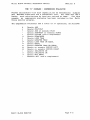
Appendix H
Multi Slave Product Re£erence Hanual
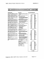
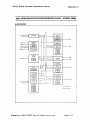
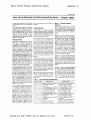
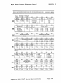
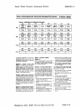
DUAL ASYNCHRONOUS RECEIVER/TRANSMITTER (DUARn
SCN2681 SERIES
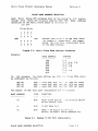
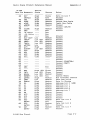
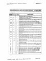
PIN DESIGNATION
APPLICABLE
MNEMONIC
NAME AND FUNCTION
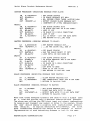
X
1/0
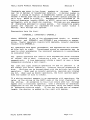
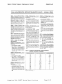
Data BUI: Bldirectional3·state data bus used to transfer commands, data and status between
the OUART and the CPU. DO is the least significant bit.
X
I
X
I
X
X
I
IWrit. Strobo: When lOW and CEN IS also lOW, the contents of the data bus is loaded into the
, addressed register. The transfer cccurs on the rising edga of tha signal.
II R."d Strob.: When low and CEN IS also low, causes tha contants of the addrassed reoister to
X
X
I
I
X
X
I
I Ruot: A t-Igh Ip.vel clears internal registers (SRA, SRB, IMR,ISR, OPR, OPCR), putsOPO-OP7
In the high state, stops the counterltllT':er, and puts cnannp.ls A and B in the inactiva stata,
INlth lhe TxOA and TxOB outputs in the m,lIk (high) state.
0
! Intorrupt R~u •• t: Active low, open drain, output which signals the CPU that one or m"re of
I
!Crystal 1: Crystal or external clock input. A crystal or clock of the specified limits must be
21
24
DO-D7
X
X
CEN
X
X
WRN
X
X
X
RON
AO-A3
i
i
I
I
I X
I
INTRN
X
X
X
X
X1'ClK
i
I
I
I
I
I
Chip Enablo: Active low Input signal. Wtlen lOW, data transfers oetween the CPU and the
OUART are enabled on 00-07 as contrOlled by the WRN, RON and AO-Al inputs. When high,
I places the 00-07 lines in the 3·stato condition.
be presented on the I'jata bus, The read cycle begins on tha falling edga of RON.
X
RESET
I
I
II
TYPE
40
)(
I
I I
iI X I
i the eight
I
I
I
Addr8ac Inputl: Sele~t the OUART int~rnal registers and ports for readJwrite operations.
maskabl~
Interrupting conditions are true.
Isuppl!ed .It all times. When a crystal is used, a capaCitor must be connected from thiS pin to
Iground (see figure 5).
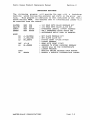
0
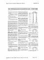
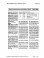
/CryDtll.2: Connect.ion for ottler side of ttle crystal. Should be conO'lcted to ground if a
Icrystal IS not used. When a crystal IS used. a capacitor must be connected from tttis pin to
Iground (see figure 5).
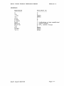
Channel A Rocolv~r S.rlol olt. Input: The least significant bi. t is received first, 'Mark' IS high,
'space' is low.
•
X
X
RlCOA
X
X
X
RxOB
X
X
X
TxOA
X
X
x
o
I
Tx08
x
X
x
o
IChannol B Transmltt.r Ser'.' Oata Output: The least significant bit is transmitted first. This
X2
Ii
Chann.' B Rocolvor Sorlal Oat. Input: The least significant bit IS received first. 'Mark' is high ..
'space' IS low.
Chann.1 A Transmltt., Sorl.1 Data Output: The least significant bit is transmitted first. ThiS
output IS held 10 the 'mark' condition wtlen "",e transmitter is disabled, idle, or when operat"
, 109 In local ioopback mode. 'Mark' ,s tllgh, 'space' IS low.
! output is tleld in the 'mark' condit,,)n when the transmitter is disabled, Idle, or when operat·
ling in local 100~bacK mode. 'Mark' IS high, ·space' is lOIN.
OPO
o
OP1
o
OP2
o
OP3
o
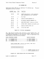
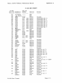
i OutPLIt 3: General purpose output, or open dralO. active low counterltimer output, or channel
OP4
o
OP5
o
IOutput 4: General purpose output, or channel A open drain, active low, RlCRDYAlFFULLA out·
Iput.
OPS
o
OP7
o
I Output 0: General purpose output. or channel A request to send (RTSAN, active lOIN). Can be
;jeactivated on receive or transmit
: Output 1: General puro;)se output. or c~al'r.el B request to send (RTSBN. actil;8 reIN). Can be
!deactivated on receive or transmit.
IOutput 2: General purpose output, or channel A transmitter 1X or t6X clock output, or chan-
Inel bo receiver IX clock output.
B transmitter tX clock output, or channel B receiver IX clock output.
~~?ut5: General purpose output, or channel B open drain, active low, RlCRO'tB/FFULLB out·
I
Output 6: GeMral purpose output, or channel A open drain, active low. TxROYA output.
Output 7: General purpose output, or Channel B open draIn, active low, TxROYB output.
IPO
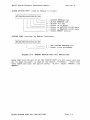
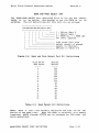
Input 0: General purpose input, or channel A. clear to send act iva low input iCTSAN).
IP1
Input 1: General purpose input, or channel B clear to 'lend active low Input (CTSBN,.
IP2
Input 2: General purpose Input, or counterllimer external clock input.
IP3
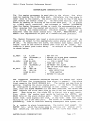
Input 3: General purpose IOput, or channel A transmitter external clock input (TxCA). When
the external clock is used by the transmitter, the transmitted data is clocked on the falling
edge of the clock.
Signe~ics 2681 DUART Device Speci£ications
Page H-3