1
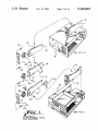
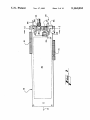
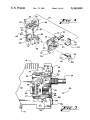
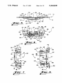
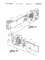
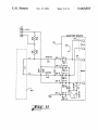
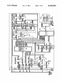
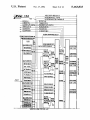
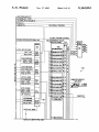
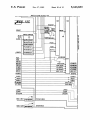
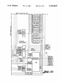
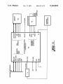
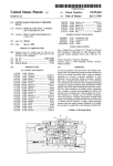
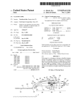
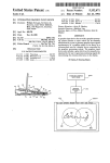
llllllllllllllIllIlllllllllllllllllllllllllllllllllIllllllllllllllllllllll
USO05163833A
United States Patent [191
[11]
[45]
Olsen et al.
[54]
DUAL PERSONAL COMPUTER
ARCHITECTURE PERIPHERAL ADAPTER
BOARD
[751 Inventors: Derek S. Olsen, San Jose; Richard D.
Cavaness, Fremont; Gail R. Snyder,
San Jose, all of Calif.
[73] Assignee: Digital Communications Associates,
Inc., Alpharetta, Ga.
Int. Cl.5 ............................................. .. HOSK 7/10
Field of Search ........... .. 439/59, 61, 62, 170-173,
439/65, 79, 80; 361/399, 413, 415, 427; 364/708
Meade et al. .
Huston, Jr. ....................... .. 364/200
4,291.370
Charles
. . . ..
4,309,754 l/1982 Dinwiddie, Jr.
Adcock
4,447,878
5/1984 Kinnie et a1.
4,473,755
4,575,793
9/1984
3/1986
364/200
364/200
... .. .. ....
. . . ..
364/200
364/200
Imani et a1. .............. ..
307/101
Morel et a1. ................... .. 364/200
4,901,205
4,936,785
4,885,482 12/1989
2/1990
6/1990 Krug
Sharp
Landiseteteta1.
a1.
a1.. ......................... .. 439/75
FOREIGN PATENT DOCUMENTS
08801008
9/1988
function for the board and circuit is a terminal emulator,
which allows a personal computer into which the board
is plugged to function as a terminal for a mainframe or
minicomputer. Edge connectors or contacts are pro
the edge connectors is compatible with a different com
puter bus, The adapter board may be ?ipped over to
3,993,936 11/1976
4,287,563 9/1981
. . . . . r . . . ..
ABSTRACT
A peripheral adapter board and circuit which is capable
for operation with two different personal computer bus
architectures is disclosed. The preferred peripheral
vided on opposite side edges of the board; each one of
References Cited
U.S. PATENT DOCUMENTS
4/1984
nection”; Computer Design, vol. 23, No. 2, Feb. 1984,
pp. 231-236.
[57]
US. Cl. .................................... .. 439/61; 361/413;
4,443,846
1988, pp. 131-132, Armonk, NY, entitled “Adapter
Card for Personal Computer”.
D. Erlin, “Establishing the Micro-to-Mainframe Con
Primary Examiner—Neil Abrams
Division of Ser. No. 339,186, Apr. 14, 1989.
9/1981
OTHER PUBLICATIONS
IBM_ Bulletin, Bardo, vol. 20, No. 1, p. 89, Jun. 1977.
IBM Technical Disclosure Bulletin, vol. 31, No. 5, Oct.
Attorney, Agent, or Firm—Jones, Askew & Lunsford
439/79; 439/170
[56]
Nov. 17, 1992
user manual; 1988.
Related US. Application Data
[58]
5,163,833
Excerpt from Devlonics Terminals N.V. modem card
[21] Appl. No.: 781,510
Oct. 22, 1991
[22] Filed:
[62]
[511
[52]
Patent Number:
Date of Patent:
plug into either computer bus. A removable, reposition
able connector board assembly is provided at one end of
the board, for mounting communications connectors in
a position accessible from the back panel of a host per
sonal computer. The connector board may be reposi
tioned to maintain the orientation of the communica
tions connectors with respect to the personal computer
back panel when the adapter board is flipped over to
plug into a different computer bus. Circuitry is pro
vided for detecting the particular computer bus into
which the adapter board is plugged, and for providing
appropriate address, data, and control signals associated
with the selected computer bus.
Belgium .
0350573
l/1990 European Pat. Off, .
3808364
9/1989 Fed. Rep. of Germany .
CONVERTIBLE DUAL
BUS ADAPTER
29 Claims, 12 Drawing Sheets
US. Patent
Nov. 17, 1992
Sheet 1 of 12
5,163,833
US. Patent
Nov. 17, 1992
Sheet 2 of 12
5,163,833
US. Patent
Nov. 17, 1992
Sheet 3 of 12
5,163,833
US. Patent
Nov. 17, 1992
Sheet 5 of 12
5,163,833
US. Patent
Nov. 17, 1992
Sheet 6 0f 12
5,163,833
J2
m D. T
m
B
m29E
anr
wEmv8
w
o.
M w
m“566.0
I“II].|lIIl
1|;
I1|lI|1lr
_
_
_
_
_
_
_
_
an
a
a 1.,
4s
W
5
_
_
1.2.1
A.
4
‘We
4A
3L
a
an
w
.
m.8i\|“5.60
US. Patent
Nov. 17, 1992
_ 13A
-
INTERRUPTS ENABLE
SYSCLK
/186|NT|N
SYSCLK
l186lNTIN
ICDSETUP (AEN)
lCDSETUP (AEN)
IMEMCS16
/MEMCS16
I /coos1s
‘
5,163,833
INTERRUPT
VECTOR SELECT
TYPE
12° N
4
Sheet 8 0f 12
/CDDS16
lCDSFDBK
-/CDSFDBK
GLOBALREAHMBASESELECT
STROBESFORREGISTERBAWGO
coMIeIIIIAIIoIIPEsIsIEIIMM
160
PC
N
M‘
I I
'
'
emmmwm
BUS
M00 1 'G A REG
KIACAIUENABE
'
IIUJIMSESLCT
5; PARENT
m
E; LATCH
MCAJR-
INT TYPE
m; ATOR snIIIMsa:. 159 IIIuIsmIIIIIE “o
SE56;
'55153 L551
'
PJ ENABLE
-
IRMA ENABLE
L PCASEGMENT
“WWW
— 'BM
“AMEN-v
ENABLE
sIIIIAMsEsLcT
PJBASESLCT
—
I
$3
LATCHUUSE Q
mm
‘
IRMAENABLE
Wm, IBNMSEH
.m
PCAJR
mm“
PJ ENABLE
REARM
BASE i»
WWW
‘A.
H m LAs-LAo
152 BASE
—T
3PORTPAMEN
WWW
IGLOBAL
Mm -nw
PCAIO u E
BASESLCT
\
NIvEcIsBEcI
lRST
_.
LA2-LAO
McAIo
KAUCACUFE'B'EG
INTENABLE
__
>
—+>IIcIIIoaIsEsIc1
‘
_l
MCA CARD ENABLE
IBM ENABLEHI
1:
55
‘5
PJBASEEL
::
m1,
I:
::
1mm
comen'Per
noIIaIIsssIcI
M
m
RMBAESLCT
M
“WNW
Iu'TIImI'nIoII'
MATCH LINE T0 FIG Tao
Km
m
3
LATGIPJBASE é
Immum <
2
LA3-LA°
.
.IaeAsEEE
IAIcImaAss
E:
LAa-LAo
52
WWW
::
::
LATGIPMNSE
35
55
;:
IIIIIIIIIEEE
;;
158
%
;;
SHMBASESEECT
SIRMAENABLE
PJBASESFlFP-T
LA3- LAO E
IE
E:
'
US. Patent
Nov. 17, 1992
VECTOR SELECT
TNTEBBUPT TYPE
INTERRUPTS ENABLE
SYSCLK
/186|NT1N
Sheet 9 of 12
5,163,833
IGLOBAL REARM
GLOBAL REARM ADDRESS
STROBES FOR REGISTER BANK 160
EMULATW mm
‘
REGISTER BANK PC
was
'
168
016g; ,1‘.
Hmmsume
MD a/WR
necooe 5i
_ WSUAUSOUNDREG
E:
_,cLPsonAmmEe
_
grain;
—
PCA
-:
m
I:
W #1:
.
g»
LATCH IBM BASE
LATCH SIRMA BASE
-:
‘m
_$IERMINALIDREG
LATCH PJ BASE
Ii
LATCH IRMA BASE
H
'|
IRD &/WR
PJ
1;
DEOODE E:
LATCH JR BASE
LA3 - LAo
JR
-» CONTROL REG
:1
m
050002 :5
’
scm
m
_;PAEMDPEG
— “mm
-
&
~
900
‘AM’
:3
H
T
‘
1
'
' v
120
(/
,
E
V
P-EB7ESTATUSHEG B.
‘
if
1 Mamas
‘
;:
_
'
PAEGMBEG
ummessw?
JR TIMING
::
:2
*
INTERRUPH86
(167
“SIRMAONLY
mum
necoos
LATCH ALL BASE
\
PJaMmBTAcEs
COMPUTERTNTERFACE
GATEARRAY
133
i
MATCH LINE T0 FIG 13D
DATA
, BUS
I:
m. 5-‘
WCHMBASE
‘ 190
REG
m0 8‘ IWR
LATCHRMBASE
mo &/WR
cum ‘ IIRQA ,
JR
‘
_
;:
LA3 - LAO
Ma
— WWW
:~
mm & NVR
LA3 - LAO
I
mmmm
LA2 _ LAO
GLOBALREARMBASE
T0FLM1AI3TNCGAEH
1Q
~
LATCH SETUP BAsE
1m
$6?
[186mm
:
1
5,163,833
2
PC/AT adapter cards, as well as to provide an upgrade
path to a 32-bit architecture which is compatible with at
DUAL PERSONAL COMPUTER ARCHITECTURE
PERIPHERAL ADAPTER BOARD
least some existing interface adapters. Many computer
installations will inevitably wind up with a mix of MCA
5 machines, PCA machines, EISA machines, and perhaps
CROSS REFERENCE TO RELATED
APPLICATION
even other personal computer architectures such as the
NuBus architecture. The proliferation of bus architec
This is a division of application Ser. No. 07/339,186,
tures has created a need for interface adapter boards for
?led Apr. 14, 1989, by Olsen et al., entitled “Dual Per
sonal Computer Architecture Peripheral Adapter 10 personal computers which increases flexibility in mov
ing the boards from computer to computer for up
Board and Circuit”.
grades, enhancements, replacement, and the like.
TECHNICAL FIELD
A related problem faced by owners is computer in
ventory or asset maintenance and control. The need to
The present invention relates to peripheral adapter
provide a different peripheral adapter for each different
boards of the type which fit into expansion slots associ
ated with personal computers, and more particularly 5 type of personal computer utilized, even though the
basic functions of the peripheral adapters may be the
relates to a terminal emulator peripheral adapter board
same, makes the tasks of selecting, acquiring, storing,
capable of operation with two discrete computer bus
maintaining, and repairing a large number of different
architectures.
BACKGROUND OF THE INVENTION
peripheral adapters unnecessarily complicated. It
20 would be more efficient if a single function peripheral
Owners and operators of personal computers regu
larly must face the fact that changes in computer tech
nology move beyond the technology embodied in a
particular machine in which they have invested. As
adapter were operative in more than one computer bus
architecture.
Accordingly, there is a need in the computer industry
for an adapter board that is compatible with and can be
computer manufacturers advance to new generations of 25 plugged into more than one type of computer bus archi
equipment, they often change to a new bus architecture.
tecture.
An example is the adoption of Micro Channel Architec
SUMMARY OF THE INVENTION
ture (MCA) by International Business Machines Corpo
ration (IBM) for use in IBM PS/Z personal computers,
The present invention solves the aforementioned and
to replace the widely popular Personal Computer Ar
chitecture (PCA) previously used in IBM PC , PC XT,
30
other problems in the art discussed above by providing
an adapter board capable of operation with either of
two discrete computer bus architectures. The preferred
and PC AT computers. Peripheral device interface
circuits embodied in adapter cards provided with edge
adapter board is operable in at least two different com
contacts compatible with the PCA system cannot be
puter bus architecture environments: the IBM PC/AT
35
used with the MCA system, and conversely.
Thus, a user who is considering upgrading to a new
generation of computer technology which employs a
different bus architecture must replace not only the
central processing unit, but all of the peripheral device
interface adapters purchased for use in connection with
the earlier machine. This may include terminal emula
tors for communicating with mainframe computers,
environment, now commonly referred to as the Per
sonal Computer Architecture (PCA) environment, and
the PS/2 environment, now commonly referred to as
the Micro Channel Architecture (MCA).
An adapter board embodying the present invention
includes two different bus connector means, each asso
ciated with one of the two architectures, PCA and
MCA, and circuit means for interfacing between the
two different bus architectures and a peripheral func
printer interfaces, and the like. If, for example, a copo
ration decides to provide terminal emulation capability 45 tion. The disclosed peripheral function is a terminal
emulator function. The terminal emulator functions
for a large group of personal computers to enable them
which are accessible to personal computer applications
to communicate with the corporation’s mainframe com
or drivers (e.g., the known IRMA, P], IBM, and the
puter, the purchase of an adapter board for each of the
like emulator drivers) comprise both hardware re
personal computers is usually required. However, if the
corporation also is considering upgrading the personal 50 sources such as input/output ports and a display RAM,
as well as microcoded services provided by a micro
computers to machines with a different, perhaps more
processor which is dedicated for 3270 protocol han
advanced, bus architecture, it faces a dilemma. If the
dling functions.
needed capability is immediately purchased, it may
Although in the preferred embodiment the adapter
have to be purchased again in the form of new adapter
boards compatible with the new bus architecture. If the 55 board comprises a terminal emulator, other types of
peripheral functions may be implemented. Accordingly,
corporation postpones upgrading to the new bus archi
the present invention is not limited to a terminal emula
tecture, it will be sacri?cing the needed terminal emula
tor, and will also be useful for peripheral functions such
tion capability during the interim period.
modems, memory expansion cards, graphics adapters,
Another aspect of the difficulties faced by personal
computer users and owners is the current competition
between the MCA personal computer bus and the Ex
Itended Industry Standard Architecture (EISA) per
sonal computer bus. Certain manufacturers of “clones”
of the popular IBM PCA bus architecture have recently
as memory expansion board, data acquisition circuits,
graphics adapters, modems, etc.
The preferred embodiment is a 3270-type emulation
adapter which provides an IBM PC or compatible per
sonal computer or an IBM PS/2 model personal com
puter with an interface to IBM 3270 control units,
embarked upon a course of action to promote the 32-bit 65 thereby allowing the personal computers to emulate
IBM 3278 and 3279 display stations, or an IBM 3287
EISA bus as an alternative to the MCA bus. The EISA
bus is being promoted at least partly to postpone the
obsoletion of older 8-bit PC bus adapter cards and 16-bit
printer. As will be understood by those skilled in the art,
in the 3278/3279 emulation mode, the circuit appears to
3
5,163,833
a mainframe computer to be a 3278 or 3279 display
station.
In order to receive communications from a main
frame control unit or cluster controller, the preferred
embodiment includes external communication connec
tors for electrical connection and communication with
remote devices. The preferred external connector is
provided on a removable, dual position connector
board assembly which is movable between a ?rst posi
tion with respect to the adapter board and a second
position with respect to the board. Thus, the adapter
board may be used with either of the bus architectures
and the external connector board, and its associated
communications connectors, may be positioned to be
4
of two discrete computer bus architectures while pres
enting the same con?guration of external connectors
associated with the board.
It is a further object of the present invention to pro
vide a terminal emulator board or card that can be used
with a personal computer having a PCA bus architec
ture or with a different personal computer having an
MCA bus architecture.
Other objects, features and advantages will become
apparent upon review of the following detailed descrip
tion of the preferred embodiment of the invention,
when taken in conjunction with the drawing and the
appended claims.
the computer housing or cabinet.
It will be appreciated that the preferred bus connec
tor means comprise electrical edge contacts compatible
with the expansion slots of the respective bus architec
tures. In the preferred embodiment disclosed below, the
BRIEF DESCRIPTION OF THE DRAWINGS
FIG. 1 is a schematic perspective of an IBM PC/AT
personal computer and an IBM PS/Z Model 50 personal
computer, showing the removal of an adapter board
constructed in accordance with the present invention
from one of the computers and recon?guration for use
in the other computer.
FIG. 2 is a side plan view of the component side of an
external communications connector may be a BNC type
coaxial connector, an RJ-ll connector, or both.
use with an MCA computer bus architecture, without
compatible with the particular bus architecture to 15
which the board is connected while still maintaining
physical alignment with openings in the back panel of
adapter board embodying the invention, assembled for
More particularly described, the invention provides a 25 card holder, retainer, and backplate.
computer adapter board including a main circuit board,
FIG. 3 is a detailed side plan view of a removable and
and external communication connector means for en
repositionable external communication connector
abling the board to be connected to a device located off
board which forms a part of the preferred embodiment
the board, with the connector means being mounted on
shown in FIG. 2.
a removable section of the main circuit board. The 30
FIG. 4 is an exploded perspective view of the remov
removable section is received in either of two orienta
able connector board shown in FIG. 3.
tions by the main board, so as to place the external
‘FIG. 5 is a vertical cross-sectional view taken along
connector means in either of two orientations. In the
line 5—5 of FIG. 2.
preferred embodiments, the removable section is slid
FIG. 6 is a side plan view of a holder which retains
ably received within an area cut out of the main board. 35 the removable connector board of FIG. 3.
The removable section preferably includes two connec
FIG. 7 is an end plan view of the holder of FIG. 6.
tors, one of which will be positioned to engage a mating
FIG. 8 is an end plan view of the removable connec
connector on the main board in either of the two orien
tor board assembly.
tations of the removable section.
FIG. 9 is an exploded perspective view of the main
It will thus be seen that a computer user considering 40 circuit board, the removable assembly and hardware
a future upgrade to a new computer with a different bus
used to interface the adapter board with an MCA bus
architecture could purchase a needed adapter board
architecture.
embodying the present invention and have compatibil
FIG. 10 is an exploded perspective view of the main
ity with both the old and new bus architectures. The
circuit board, removable connector board assembly,
user thus will not have to replace several expensive 45 and hardware used to interface the adapter board with
adapter boards when upgrading the underlying system,
and can merely recon?gure the adapter board for the
a PCA bus architecture.
FIG. 11 is a schematic diagram of the circuitry of the
new architecture when the new computer is acquired.
removable connector board, connecting the external
Thus, it is an object of the present invention to pro
communication connectors to the main circuit board.
vide a more versatile peripheral circuit adapter board 50
FIG. 12 is a schematic block diagram of the preferred
for computers.
embodiment of a dual computer bus interface circuit
It is a further object of the present invention to pro
which is provided on the main circuit board for inter
vide an improved adapter board capable of operation
facing the adapter to a plurality of different computer
with at least two discrete bus architectures.
bus architectures.
It is a further object of the present invention to pro 55
FIG. 13 comprising FIGS. 13A-13D, is a more de
vide an improved peripheral function adapter board and
circuit for use with a plurality of different computer bus
architectures, having an improved bus interface circuit
for interfacing to the different computer bus architec
tures.
It is a further object of the present invention to pro
vide an improved peripheral function adapter circuit for
use with a plurality of different computer bus architec
tures which makes economical use of circuit compo
nents and board real estate by consolidating bus inter 65
face functions common to both bus architectures.
It is a further object of the present invention to pro
vide an adapter board capable of operation with either
tailed schematic block diagram of the computer inter
face gate array which is employed in the computer bus
interface circuit shown in FIG. 12.
FIG. 14 is a more detailed schematic block diagram
of of the JR CPU which is employed in the computer
bus interface circuit shown in FIG. 12 to effectuate 3270
communications.
DETAILED DESCRIPTION OF THE
PREFERRED EMBODIMENT
Referring now to the drawings, in which like numer
als refer to like parts throughout the several views,
FIG. 1 shows an IBM PC/AT personal computer 6,
5
5,163,833
with the preferred embodiment of the present inven
tion, a dual bus computer interface adapter board 10
6
communication protocol. It accepts and executes com
mands from both a 3270-type control unit and from the
con?gured for use in such a computer architecture,
PC. It accordingly assists the personal computer in
being removed therefrom. The adapter board 10 is
recon?gured for use in an IBM PS/Z Model 50 personal
establishing a 3270 mainframe session through cluster
controllers such as IBM type 3274, 3276, and 3174 con
computer 8 by removing thumbscrews 111, 112, remov
trol units, and IBM 4321, 4331, 4361 and 470l systems.
In the present invention, various terminal emulator
ing a PCA backplate 118, removing a removable con
nector board assembly 20, ?ipping the board 10 over in
the direction of arrows 9 so that the MCA edge connec
tor 14 is downwardly disposed and the PCA edge con
nector 16 is upwardly disposed, reinserting the remov
able connector board assembly 20, attaching MCA card
holder 114 and card retainer 115, attaching an MCA
backplate 110 with the thumbscrews 111, 112, and in
serting the recon?gured board 10 into the computer 8.
FIG. 2 shows a plan view of the dual bus computer
interface adapter board 10 embodying the present in
vention, con?gured for an MCA computer bus archi
modes are implemented with programming in the JR
CPU. Operation in a selected mode provides what is
known as a “programming interface”, that is, a prede
termined set of parameters, commands, and registers
needed by a software driver in the host PC to allow the
software driver to effectuate operation in a particular
emulator mode. The associated programming interfaces
which are operative with the present invention employ
resources provided on the preferred adapter board 10.
Several different industry standard terminal emula
tion programming interfaces or modes may be imple
mented with the preferred embodiment, allowing the
tecture. The main adapter board 10 includes a compo
nent side 11, shown in FIG. 2, and a solder side 12 (see 20 use of currently popular micro-to-mainframe software.
Such interfaces include the known IRMA, PJ, and IBM
FIG. 10). The board 10 has a longitudinal axis of sym
metry represented by a dashed line 13. Along the bot
Advanced Adapter interfaces. For further information
on these programming interfaces, see the IBM docu
tom edge of the board as viewed in FIG. 2, the board 10
ment entitled “Technical Referenced for the Advanced
includes a series of MCA edge contacts 14, which are
arranged to be plugged into an expansion slot in a com 25 Adapter”, IBM document number GA23-0302-l. See
also the Digital Communications Associates, Inc. docu
puter using MCA bus architecture. A set of PCA edge
ment entitled DCA IRMA 2 Technical Reference
contacts 16 for a PCA expansion slot are positioned
along the top of the board 10, generally opposite the
MCA edge contacts.
.
Guide, document number 40-97920-000, published by
the assignee of the present invention.
Inasmuch as these types of terminal emulation modes
The preferred embodiment of a dual bus interface 30
will be known to those skilled in the art, further discus
adapter 10 disclosed herein operates to con?gure a
sion of same will not be provided herein, other than to
personal computer into which the adapter is plugged
into a terminal emulator for a mainframe computer,
say that the disclosed adapter is programmed to imple
although other computer interface functions will be
ment such mainframe terminal emulation interfaces.
come apparent to those skilled in the art. Accordingly, 35
circuitry 30 is provided on the board 10 for executing
the terminal emulator peripheral function. Although in
the preferred embodiment, the adapter board circuitry
30 comprises a terminal emulator, it should be under
stood that other types of peripheral functions may be
implemented. Thus, the circuit 30 may be a memory
expansion circuit, a color graphics monitor driver
/adapter, a data acquisition circuit, a modem, a disk
drive or tape drive controller, or any of a number of
other computer peripheral functions.
As discussed above, the preferred adapter board 10 is
operable in at least two different computer bus architec
ture environments: the IBM PC/AT environment, now
commonly referred to as the Personal Computer Archi
tecture (PCA) environment, and the PS/2 environment,
now commonly referred to as the Micro Channel Ar
chitecture (MCA). The terminal emulator functions
which are accessible to personal computer applications
or drivers (e.g., IRMA, PJ, IBM Advanced Adapter,
and the like) comprise both hardware resources such as
input/output ports and a display or “multi port” RAM,
as well as microcoded services provided by the dedi
cated JR microprocessor.
As will be understood by those skilled in the art, in
The disclosed embodiment is a 3270-type emulation
adapter which provides an IBM PC/AT or compatible
personal computer or an IBM PS/Z MCA or compati
the 3278/3279 emulation mode, the circuit appears to a
ble model personal computer with an interface to IBM
3270 control units, thereby allowing the personal com 50 mainframe computer to be a 3278 or 3279 display sta
tion. The circuit decodes and executes commands from
puters to emulate IBM 3278 and 3279 display stations,
established over a conventional IBM category A coax
a control unit or cluster controller, to cause updating of
a display buffer located on the board and to process
ial cable at distances at up to 5,000 feet utilizing external
keystrokes. The preferred adapter board includes
or an IBM 3287 printer. The communication link is
communications connector 24, or a conventional IBM 55 enough display buffer memory to accommodate IBM
type 3 twisted pair cable at distances at up to 1,000 feet
utilizing external communications connector 25. For
further information about the 3270 protocols, see the
IBM documents entitled “IBM 3270 Connection Tech
nical Reference," IBM document number GA23-0339-0
or “IBM 3174/3274 Control Unit to Device Product
327X screen models 2 through 5, and to support the
IBM Extended Attribute Buffer (EAB) for each model.
Software which executes on the personal computer'
stimulates the adapter board circuit 30 to transfer a
copy of the display buffer to the personal computer
video board when screen updates occur. Keystrokes
from the personal computer’s keyboard are submitted to
Attachment Information (PAI)” dated October 1986.
the adapter circuit, and the adapter 10 sends them to the
The preferred adapter circuit includes an on-board
control unit in the appropriate protocol.
dedicated processor denominated the JR CPU (de
scribed below in connection with the preferred cir 65 Another mode of operation is the 3287 mode. In this
mode, the preferred circuit described herein appears to
cuitry 30) for managing the 3270 communications func
be a 3287 printer to a control unit. The adapter circuit
tions, which thereby off-loads the host personal com
decodes and executes commands from the control unit
puter from the real-time processing requirement of
7
5,163,833
8
that similarly update the display or print buffer and
solicits printer status. The display buffer is used by the
connector 29, depending upon the orientation of the
circuit to buffer print data and a control block. Soft
ware executing on the personal computer moves a copy
of the buffered print data to a printer attached to the
nector board assembly 20 is changed between its two
possible orientations, the particular one of the female
connector board assembly 20. As the removable con
connectors 27 and 28 which is on the component side 11
personal computer and acknowledges print completion
of the main board is located directly adjacent to the
or a printing error.
male connector 29.
Yet another mode of operation possible with the
disclosed embodiment is known as the DFT mode,
wherein the adapter circuit appears to be a gateway to
an intelligent workstation. The adapter circuit decodes
and executes commands from a control unit and updates
a display buffer. The display buffer is used to buffer a
3270 data stream commands and communication status.
These commands may be addressed to a plurality of 15
logical displays and a printer. Such intelligent worksta
tions are capable of processing 3270 data streams, man
aging formatted display screens, and handling local
keystroke processing.
These and other modes of operation may occur to
those skilled in the art after the discussion which fol
lows.
Referring still to FIG. 2, in order to communicate
The removable board 35 also includes circuitry 38 for
connecting the BNC external communications connec
tor 24 and the RJll external connectors connector 25 to
the two separate ?ve-pin connectors 27 and 28, as
shown in FIG. 11, and then to an analog interface cir
cuit 40 on the adapter 10. The analog interface circuit
40 comprises a conventional circuit known for use in
3270 communications, and will not be described further
herein. The circuitry 38 comprises a parallel connection
between the active or signal-carrying terminals of the
RJ ll connector 25 and the BNC connector 24. The
active or signal-carrying terminals are provided as pins
27-1 and 28-1, signal return is provided on the pins 27-2,
28-2, 27-3, 28-3, 27-5, 28-5, while DC ground is pro
vided on pins 274, 284. These pins mate with respec
tive pins 29-1, 29-2, 29-3, 29-4, and 29-5 of the male
with a cluster controller (such as an IBM 3274, 3276, or
connector 29. A transient voltage absorber CR1 such as
3174 Control Unit) or other control unit, an external 25 as General Instruments 1N6267 and filter capacitors C1,
communications connector comprising a removable
C2 provide for noise ?ltering between DC ground and
connector board assembly 20 is ?tted into the main
chassis/frame ground in the known manner.
adapter board 10 at the rear end of the board (the right
Incoming communications signals are applied to con
side of the board 10 in FIG. 2). The removable connec
nectors 24, 25, coupled through capacitor C5 and
tor board assembly 20 may be associated with the board
brought to a pulse transformer T1 in the analog inter
10 in either of two orientations, as explained in detail
face circuit 40, which passes the difference between the
below. The connector board assembly 20, being con?g
ured as a terminal emulation adapter circuit, carries two
external connectors in the preferred embodiment-a
two signal lines through to a voltage comparator (not
shown) for conversion to T'I'L levels. Outgoing com
munications signals are applied to a separate winding of
coaxial connector 24 and an RJll connector 25-—which 35 T1, passed through capacitor C5, and applied to con
are accessible from the back panel of the computer
nectors 24, 25 and the external cable. Received data
when the board 10 is installed in an expansion slot. The
decoding is performed by receiver logic internal to the
connector board assembly 20 also includes a pair of
JR CPU 122, described in connection with FIG. 12.
female multi-pin header connectors 27 and 28 (see FIG.
Encoding of the transmitted data is performed by trans
4) positioned for one of them to receive the pins of a 40 mitter logic also internal to the JR CPU 122. A jumper
corresponding male multi-pin connector 29 located on
12 allows for connection of terminating resistors R35 or
the main board 10 when the connector board assembly
R36 between the terminals of the pulse transformer T1,
20 is installed into the main board 10.
depending upon whether the RJ ll or BNC connection
Processing of communications between the cluster
is used, for impedance matching of the transformer
controller or other control unit and the personal com 45 circuit to the requirements of the communications lines
puter into which the preferred adapter 10 is plugged,
connected.
including protocol decoding and encoding, mainte
Turning now to FIGS. 3 and 4, it will be seen that a
nance of display memory, etc., are effectuated through
circuit 30, which is described later.
As shown in FIGS. 3 and 4, the removable connector
board assembly 20 includes a removable printed circuit
board section 35 and a holder 60 which supports the
removable board 35 and enables it to be inserted or
removed from its installed relationship to the main
pair of notches 57 and 58 are formed in the top and
bottom edges, respectively, of the removable board 35
of the connector board assembly 20, near the front edge
thereof. These notches assist in locating the board 35
with respect to the holder 60, which is'shown in FIGS.
3-8. The holder 60 is preferably molded from a unitary
piece of non-conductive plastic material which may be
board 10. The board 35 has a component side 36 and a 55 one of several appropriate types known to those skilled
solder side 37. The external communications connectors
24 and 25 noted above are positioned along the rear
in the art. A planar base 62 is formed with a pair of
edge of the board 35, such that the female portion of the
coaxial/ENC connector 24 extends beyond the edge of
base 62 along opposite edges thereof. The angled walls
angled walls 63 and 64 extending out of the plane of the
63 and 64 end in a pair of ledges 65 and 66, respectively.
the main board when the removable connector board
As shown in FIGS. 5 and 8, the removable board 35
assembly 20 is installed as shown in FIGS. 2 and 3. The
rests on the ledges 65 and 66 spaced apart in relation to
RJll connector 25 is a female connector positioned to
the base 62, with the female 5-pin connector 28 extend
extend beyond the rear edge of the main board 10. The
ing into the space between the base 62 and the board 35.
female terminal connectors 27 and 28 are positioned at
A pair of U-shaped tracks 70 and 71 are provided in
the rear edge of the removable board 35, with the con 65 the holder 60 extending adjacent to the ledges 65 and
nector 27 on the component side 36 and the connector
66. The tracks open away from the center of the holder
28 on the solder side 37. The connectors 27, 28 are
60 in the plane of the board 35, and are just wide enough
identical, so that either of them can mate with the male
to slidably receive the main board 10, in a manner de
5,163,833
scribed below. A pair of cutouts 68 and 69 are provided
in the angled walls 63 and 64 and the base 62 to permit
movement of the resilient latches 74 and 75, which
extend above the ledges 65 and 66. As shown best in
FIG. 5, these latches 74, 75 de?ne a bevelled surface
and can be urged outwardly during installation of the
removable board 35, whereupon they spring back over
10
85 and 86, and when the board 35 is fully installed, the
openings 97 and 98 are aligned with the cutouts 90 and
91 of the posts.
Referring now to FIG. 9, the main adapter board 10
de?nes a generally square cutout 105 shaped to mat
ingly receive the removable connector board assembly
20. The cutout 105 is centered on the axis of symmetry
13 (FIG. 2) and opens to the rear edge of the main board
10. Holes 106 and 107 are formed in the main board
place.
The holder 60 also de?nes a transverse support wall . .a O adjacent to the cutout 105 to receive the detents 82 and
83 of the locking tabs 80 and 81 of the holder 60.
77 extending between the angled walls 63 and 64 be
The removable connector board assembly 20 may be
tween the cutouts 68 and 69 and the front edge of the
assembled with the main board 10 in either of two con
holder 60. The support wall rises from the base 62 to a
the upper and lower edges of the board 35 to hold it in
height even with that of the ledges 65 and 66, and helps
both to give rigidity to the holder 60 and to prevent the
board 35 from bowing toward the base 62.
Near the front edge of the holder 60, a pair of locking
tabs 80 and 81 extend outwardly from the holder at the
level of the ledges 65 and 66 to a position beyond the
tracks 70 and 71. The tabs 80 and 81 carry detents 82 20
and 83, respectively, which project slightly into the
?gurations, shown in FIGS. 9 and 10. To install the
removable connector board for operation with an MCA
architecture, the tracks 70 and 71 are aligned with the
top and bottom edges of the cutout 105, with the com
ponent side 36 of the removable board 35 facing the
same direction as the component side 11 of the main
board 10. Then, the tracks 70 and 71 are slid onto the
main board. When the detents 82 and 83 engage the rear
edge of the main board 10, the tabs 80 and 81 ?ex to
plane of the main board 10, as shown in FIG. 5, to catch
allow the detents to slide over the solder side surface of
in openings in the main board as described below, and
the board 10. The removable assembly is moved into the
retain the connector board assembly 20 in place. The
thickness of the tabs 80 and 81, and the resilient nature 25 main board 10 until the pins of the male terminal 29
insert into the sockets of the female terminal connector
of the plastic material, should be such that the tabs can
27, and the detents 82 and 83 enter the holes 106 and
?ex by at least the height of the detents 82 and 83.
At the two rear corners of the holder 60, a pair of
posts 85 and 86 extend at right angles away from the
base 62 on the concave side of the holder 60. A pair of
?anges 87 and 88 extend inwardly along the inner edges
of the posts 85 and 86. The ?anges 87 and 88 are shaped
and spaced apart to matingly receive the notches 57 and
58 provided in the removable board 35. The posts 85
and 86 also de?ne cutout slots 90 and 91 positioned to
align with holes in a standard backplate, as described
below.
A pair of conductive U-shaped grounding clips 95
107. The fully installed MCA configuration is shown in
FIGS. 2, 3, and 9.
To install the MCA con?gured adapter board 10 into
a computer, the MCA card holder 114 and card retainer
115 are snapped onto the board 10. An MCA backplate
110 is secured to the board by aligning the holes in the
backplate with the openings 97 and 98 in the grounding
clips 95 and 96. The backplate 110 is secured by thread
ing a pair of thumbscrews 111 and 112 through the
openings in the backplate and into the openings 97 and
98. Other openings in the backplate allow the coaxial
connector 24 to extend through the backplate, and
and 96 are ?tted onto the extending ends of the posts 85
and 86. The clips 95 and 96 de?ne openings 97 and 98 40 allow access to the R111 connector 25. The board is
now ready to be inserted into the computer with the
which align with the slots 90 and 91 on the holder 60
edge contacts 14 engaging an MCA expansion slot (not
and threadably receive standard thumbscrews as de
scribedbelow. The clips 95 and 96 include extensions
shown).
It should be understood that the MCA card holder
100 and 101 that wrap around the ?anges 87 and 88 of
the posts 85 and 86, and de?ne pin sets 102 and 103 45 114 and card retainer 115 are not standard IBM MCA
card holders and retainers. The standard IBM-type card
which are soldered or press fit to the removable board
holders and retainers are permanently attached to stan
35 as shown in FIG. 4.
To assemble the removable connector board assem
bly 20, one needs the parts shown in FIG. 4, namely, the
removable board section 35, the holder 60, and the
grounding clips 95 and 96. The clips 95 and 96 may
initially be soldered or press ?t to the board 35 after
dard IBM MCA printed circuit boards by rivets,
whereas the preferred card holder 114 and card retainer
115 employed in the present invention are removable so
as to allow removal and recon?guration of the board
for use in a PCA environment.
placing the pin sets 102 and 103 in appropriate openings
To recon?gure the board for a computer utilizing a
in the printed circuit board 35. Then, the board 35 and
the holder 60 are moved together until the notches 57
and 58 engage the ?anges 87 and 88. The board 35 slides
PCA architecture, the thumb screws 111 and 112 are
along the ?anges 87 and 88 until it meets the bevelled
surfaces of the resilient latches 74 and 75. Pressure is
exerted on the board 35 to cause its edges to move the
removed, then the MCA backplate 110, card holder
114, and card retainer 115 are removed. The removable
connector board assembly 20 then may be grasped and
pulled outwardly, sliding the tracks 70, 71 along the
edges of the cutout 105 while disengaging the female
latches outwardly, allowing the board 35 to move past 60 connector 27 away from the male connector 29, and
dislodging the detents 82 and 83 from the holes 106 and
the latches until it rests against the ledges 65 and 66,
107. When the removable connector board assembly 20
whereupon the latches spring back above the board 35
is clear of the main board 10, it is rotated 180 degrees so
and hold it ?rmly against the ledges and the support
that the solder side 37 (FIG. 4) of the removable board
wall 77. Lateral movement of the board 35 is con?ned
35 and the base 62 of the holder face in the same direc
by the ?anges 87 and 88, and by the inner walls of the
tion as the component side 11 of the main board 10, as
tracks 70 and 71, which extend above the level of the
shown in FIG. 10. The removable connector board
ledges 65 and 66. As the the board moves toward the
assembly 20 may then be slid onto the main board
‘ ledges, the U-shaped clips 95 and 96 slide over the posts
11
5,163,833
12
within the cutout 105 in the same manner as described
As will be understood by those skilled in the art,
above. The detents 82 and 83 move along the compo
nent side surface of the main board 10, and enter the
buses such as the MCA bus 14 and the PCA bus 16
peripheral device interfaces for different computer
holes 106 and 107 from the opposite side as previously
typically carry out many of the same basic functions,
described. The female connector 28 is now aligned with
the male connector terminal 29, and the two become
coupled as the connector board assembly 20 reaches its
namely, receiving address information from address
signals, decoding the address signals to determine if the
particular peripheral circuit is being addressed by a host
fully inserted position (not shown).
CPU, receiving and transmitting data signals, generat
ing and processing interrupts, timing to accommodate
Still referring to FIG. 10, to install the PCA con?g
the various cycles on the buses, and performing other
Iured adapter board 10 into a computer, a PCA back
types of computer system control functions. While
plate 118 is secured to the board by aligning the holes in
there are various (and often substantial) differences
the backplate with the openings 97 and 98 in the
between the MCA bus and the PCA bus, including but
grounding clips 95 and 96. The backplate 118 is secured
not limited to the pinouts of the bus connectors and the
by threading the thumbscrews 111 and 112 through the
openings in the backplate and into the openings 97 and 15 physical dimensions of the contacts on the edge connec
tors, there are nonetheless similarities.
98. The board 10 is then ready to be inserted into the
The present invention capitalizes on the similarities
computer with the edge contacts 16 engaging a PCA
expansion slot (not shown).
It thus will be seen that when the removable connec
tor board assembly 20 is changed from an MCA orienta
tion to a PCA con?guration, and conversely, the exter
nal communications connectors 24 and 25 change from
between functions common to both bus architectures.
Signi?cant efficiencies in usage of board real estate and
components are obtained in the present invention by
providing computer interface functions common to
both buses and providing services to both buses through
a custom VLSI computer interface gate array 120,
while still allowing for the differences between the
positions extending above the component side of the
main board 10 to positions extending above the solder
25 buses. The computer interface gate array 120 performs
side of the main board. Since the coaxial connector 24
and the RJ 11 connector 25 are on opposite sides of the
axis of symmetry 13 (see FIG. 2), they also exchange
most of computer interface services and functions com
mon to both the PCA and the MCA bus.
Referring in this regard to FIG. 12, the address lines
positions with respect to the axis of symmetry 13 when
the con?guration of the removable assembly 20 is 30 ADO-A19 of both the MCA bus 14 and the PCA bus 16
are provided to the computer interface gate array 120
switched.
for decoding. Since the MCA bus 14 includes more
It will also be appreciated that the mechanical recon
address lines than the PCA bus, the address lines A2
?gurability of the preferred adapter board described
0-A23 of the MCA bus are provided to a card select
above can easily be adapted for use with other types of
address decode circuit 126 for decoding whether the
peripheral devices and connectors for purposes other 35 particular adapter card 10 is being addressed on the
than a terminal emulator, while still remaining within
MCA bus. The output of the decoder 126 is a signal
the scope of the present invention. For example, if the
denominated/ADSEL, which becomes low true when
adapter 10 is employed as a graphics interface for a high
the particular adapter is addressed on the MCA bus.
resolution RGB monitor, a monitdr cable connector
(Note: for purposes of the following discussion, a slash
(not shown) may be mounted on the'connector board 40 “/” preceding a signal name signi?es a low true signal.)
assembly 20, and the connector repositioned with re
The determination of whether the PCA bus 16 or the
spect to the back of the computer cabinet to maintain
MCA bus 14 is active is made by signal denominated
alignment with openings in the back. It will be therefore
MCA UNIQUE GROUND, provided on line 128. This
be appreciated that the present invention is operable
signal, also denominated PCMDL, is derived from one
with a wide variety of personal computer peripheral 45 of the pins of the MCA bus 14 which is grounded only
functions.
when the adapter is plugged into an MCA bus; the line
is pulled up to ?ve volts by a pullup resistor R2, so that
Preferred Circuitry
if the adapter board is plugged into a PCA bus 16, the
Inasmuch as the disclosed embodiment of the present
signal PCMDL will be high. The PCMDL signal ac
invention of a dual computer architecture peripheral 50 cordingly identi?es which of the two different com
adapter comprises a terminal emulator as the peripheral
puter architectures is being employed.
function, next will be described the preferred interface
Data signals D00-D07 from both the MCA bus 14
circuitry for interfacing two different personal com
and the PCA bus 16 are provided to a low byte_trans
puter architectures, the PCA architecture and the MCA . ceiver circuit 130, which is a bidirectional circuit. The
architecture, to a terminal emulator peripheral function. 55 data signals or bus BDO-BD7 from the transceiver 130
Turning in this regard to FIG. 12, the preferred cir
are then provided to the computer interface gate array
cuitry 30 for interfacing the adapter board to the PCA
120, as well as to the JR CPU 122, for data transfers.
and MCA computer architectures is shown, with the
The data lines BDO-BD7 are considered as the low byte
particular peripheral function of providing a terminal
of a 16-bit data path.
emulation circuit for effectuating 3270 emulation proto 60 Those skilled in the art will understand that the MCA
‘ cols. The preferred interface circuit 30 is constructed
bus 14, being either an 8, 16, or a 32-bit bus, includes at
around a computer interface gate array 120 and a dedi
least additional data signals DOS-D15. These line are
cated microprocessing circuit or CPU 122, designated
considered the high byte of a 16-bit data path. In a
the JR CPU, for carrying out 3270 protocol functions.
con?guration wherein the adapter is operative as a
Signals constituting 3270 communications are received 65 16-bit bus, the data signals D08-D15 from the MCA bus
via the BNC/coax connector 24 or the R111 connector
14 are provided to a high byte driver 131, which buffers
25 at an analog interface circuit 40, which is connected
the high data byte to data lines BD08-BD15. The high
for communications with the JR CPU 122.
byte lines BD08-BD15 are provided to a high byte
13
5,163,833
transceiver 132, as well as to a high byte random access
memory (RAM) 134. The high byte RAM 134 consti
tutes part of the triple port RAM, is preferably an 8K by
8 or 32K by 8 static RAM. The RAM 134 is addressed
by the address lines MAO-MA7, which are provided as
output address lines from the gate array 120. The RAM
134, 136 can be expanded to a total of 64K bytes, if 32K
bytes RAM chips are employed.
It will be understood that data for the high byte
RAM 134 may originate either from the host bus line
D08-D15, or internally via internal data lines
MDO~MD7. If data originates on the data lines
MDO-MD7, it passes through the high byte transceiver
132. The data lines MDO-MD7 are an internal data bus
which is connected between the high byte transceiver
132, the computer interface gate array 120, the low byte
RAM 136, and a program read-only memory (ROM)
138. Both the RAM 134, 136, and the ROM 138 may be
14
gate array 120 is being used in a PCA environment, the
input switch information is used to establish base ad
dress locations for resources installed on the adapter.
This must be done to ensure that no two devices (the
adapter and another peripheral device) share the same
address space.
Turning next to FIG. 13, the computer interface gate
array circuit 120 is preferably constructed as a custom
or semicustom VLSI gate array. The primary func
tional blocks of the computer interface gate array 120
include a latch circuit 150 which is used to latch in
various address information and status information
which may be transitory, address multiplexers 152, 153,
157, 158, a con?guration register bank 160 for storing
information concerning the setup, a peripheral function
or emulator register bank 162 for storing information
speci?c to the execution of the adapter’s particular
function (in this case, terminal emulation), decoder cir
cuits 168, 169, a triple port RAM controller 165, a PC
20 cycle control circuit 170, a switch capture circuit 175, a
the address lines MAO-MA7 and BAO-BA7.
JR CPU monitor and control circuit 180, and an inter
Control signals such as clocks, address strobes, mem
rupt control 190.
ory refresh signals and the like from both the MCA bus
The configuration register 160 stores configuration
14 and the PCA bus 16 are provided as the signals de
data downloaded via a PC DATA BUS. The register
nominated SYSTEM CONTROL BUS to the com
puter interface gate array 120. Interrupt request signals 25 includes an MCA con?guration register MCA CON
FIG ‘A’ REG, dual purpose MCA and PCA con?gura
such as /IRQA-/IRQD from both the MCA bus 14 and
tion registers MCA & PCA CONFIG ‘B’ REG and
the PCA bus 16 are also provided to the gate array 120.
MCA & PCA CONFIG ‘C’ REG, and an MCA CON
As will be discussed in greater detail below, the com
FIG ‘D’ REG.
puter interface gate array 120 includes a plurality of
The incoming address lines ADO-A19 are provided to
data storage registers required for implementing the
various locations in the circuit 120, including a-pro
various 3270 protocol and mainframe communication
up to a total of 64K bytes each and are addressed with
functions. Accordingly, signals emanating from the
grammable base address comparator 156. Address lines
computer interface gate array 120 include address lines
MAO-MA7, which form a memory address for the
ADO-A12 are provided to the latch circuit 150 for stor
age of these bits of the address as the latched address
memories 134, 136, 138. An address latch 140 buffers
signals LA00-LA12. The base address comparator 156
the address signals MAO-MA7 and forms a low address
compares the incoming addresses to various base ad
comprising signals BAD-HA7, which are provided to
dresses, and provides output signals at the beginning of
the memories.
The gate array also generates MEMORY CON
a bus cycle indicating that a selected base address has
occurred on the address bus. The base addresses corre
TROL signals for the memories 134, 136, 138. These 40 spond to addresses in the address space of the host CPU
assigned to a particular programming interface.
signals are provided to a memory control programmed
Output signals from the base address comparator 156
logic array (PAL) 142, which provides speci?c memory
include the signals RAM BASE, ROM BASE, JR
control signals for controlling the reading from and
BASE, PJ BASE, IRMA'BASE, SIRMA BASE, IBM
writing to the memories.
The JR CPU 122, being a dedicated special purpose 45 BASE, and GLOBAL REARM BASE. These output
signals are provided to the latch 150. The signal denom
computer itself, is able to address memory to access
instructions and data in a manner similar to other com
inated RAM BASE occurs when the address on the
puters. Accordingly, address signals CA00-CA13 are
address lines ADO-A19 corresponds to the address PCA
SEGMENT or MCA RAM BASE SLCT, depending
upon whether PCA mode or MCA mode, respectively,
provided as a bus between the computer interface gate
array 120, the JR CPU 122, and a microcode RAM
1440, 144b. The microcode RAM 144 is preferably 8K
is selected by the select signal PCMDL. A multiplexer
by 8 static RAM, and provides data buses denominated
157 selects between these two address segments, de
CDO-CD7 and CD08-CD15.
The RAM 144 is employed for storage of instructions
for the JR CPU 122. These instructions are download
from a host PC, and con?gure the JR CPU to operate in
pending upon the mode selected. RAM BASE and
subsequently PC MEMREQ (from decoder 168) indi
cates that the triple port RAM 134, 136 has been se
lected by the host PC for a read or write operation.
one of a plurality of different emulation modes, such as
Similarly, the comparator 156 provides the signal
IRMA, PJ, IBM Advanced Adapter, and the like.
A set of option switches 146 are read by the computer
interface gate array 120 during the power up cycle. The
computer interface gate array 120 enables the switch
ROM BASE to the latch 150 in response to comparison
between the address lines ADO-A19 and an address
segment of either PCA ROM BASE SLCT or MCA
ROM BASE SLCT. These two address segments are
selected by a multiplexer 158, depending on whether
PCA or MCA mode is selected by the select signal
CDO-CD7 bus. When the computer interface gate array
PCMDL. The ROM BASE signal indicates that the
120 is being used in an MCA environment, the input
switch information is used to generate alternate adapter 65 ROM 138 has been selected for a read operation.
The address segments MCA RAM BASE SLCT and
ID information. This allows the computer interface gate
MCA ROM BASE SLCT are stored in the register
array to be used in a plurality of different designs, each
MCA CONFIG ‘D’ REG in the con?guration register
with a unique identi?er. When the computer interface
driver 147 to drive switch information onto the