1
PPC1Bug
Diagnostics Manual
PPC1DIAA/UM2
Notice
While reasonable efforts have been made to assure the accuracy of this document,
Motorola, Inc. assumes no liability resulting from any omissions in this document,
or from the use of the information obtained therein. Motorola reserves the right to
revise this document and to make changes from time to time in the content hereof
without obligation of Motorola to notify any person of such revision or changes.
No part of this material may be reproduced or copied in any tangible medium, or
stored in a retrieval system, or transmitted in any form, or by any means, radio,
electronic, mechanical, photocopying, recording or facsimile, or otherwise,
without the prior written permission of Motorola, Inc.
It is possible that this publication may contain reference to, or information about
Motorola products (machines and programs), programming, or services that are
not announced in your country. Such references or information must not be
construed to mean that Motorola intends to announce such Motorola products,
programming, or services in your country.
Restricted Rights Legend
If the documentation contained herein is supplied, directly or indirectly, to the U.S.
Government, the following notice shall apply unless otherwise agreed to in
writing by Motorola, Inc.
Use, duplication, or disclosure by the Government is subject to restrictions as set
forth in subparagraph (c)(1)(ii) of the Rights in Technical Data and Computer
Software clause at DFARS 252.227-7013.
Motorola, Inc.
Computer Group
2900 South Diablo Way
Tempe, Arizona 85282
Preface
The PPC1Bug Diagnostics Manual provides general information, installation
procedures, and a diagnostic Þrmware guide for the PPC1Bug Debugging
Package. All information contained herein is speciÞc to MotorolaÕs PowerPCªbased boards: UB60x Ultra 60x Low ProÞle Form Factor motherboards, AB60x
Atlas 60x Baby-AT Form Factor motherboards, MVME160x multi-module Single
Board computers, MVME130x PowerBase embedded controllers, and E60x
PowerStackª Series E system motherboards. In this manual, they are collectively
referred to as Òthe PowerPC boardÓ; when necessary to refer to them individually,
they are called the UB60x, AB60x, MVME160x, MVME130x, and E60x, respectively.
This manual covers release 1.9 of PPC1Bug, dated 12/19/95, and earlier versions.
Use of the PPC1Bug debugger, the debugger command set, the one-line
assembler/disassembler, and system calls for the debugging package are all
described in the PPCBug Firmware Package User's Manual (PPCBUGA1/UM2 and
PPCBUGA2/UM2).
Refer also to the lists of publications in Appendix A, Related Documentation, for
other documents that may provide helpful information.
This manual is intended for anyone who wants to design OEM systems, supply
additional capability to an existing compatible system, or work in a lab
environment for experimental purposes. A basic knowledge of computers and
digital logic is assumed.
Conventions
The following conventions are used in this document:
bold
is used for user input that you type just as it appears. Bold is also
used for commands, options and arguments to commands, and
names of programs, directories, and files.
italic
is used for names of variables to which you assign values. Italic
is also used for comments in screen displays and examples.
courier
is used for system output (e.g., screen displays, reports),
examples, and system prompts.
RETURN
represents the “carriage return” or ENTER key.
CTRL
represents the control key. Execute control characters by
pressing the CTRL key and the letter simultaneously, e.g.,
CTRL-d.
Manual Terminology
Throughout this manual, a convention has been maintained whereby data and
address parameters are preceded by a character which speciÞes the numeric
format as follows:
$
0x
%
&
dollar
Zero-x
percent
ampersand
specifies a hexadecimal character
specifies a binary number
specifies a decimal number
Unless otherwise speciÞed, all address references are in hexadecimal throughout
this manual.
An asterisk (*) following the signal name for signals which are level signiÞcant
denotes that the signal is true or valid when the signal is low.
An asterisk (*) following the signal name for signals which are edge signiÞcant
denotes that the actions initiated by that signal occur on high to low transition.
In this manual, assertion and negation are used to specify forcing a signal to a
particular state. In particular, assertion and assert refer to a signal that is active or
true; negation and negate indicate a signal that is inactive or false. These terms are
used independently of the voltage level (high or low) that they represent.
For PPC1Bug, data and address sizes are deÞned as follows:
❏
A byte is eight bits, numbered 0 through 7, with bit 0 being the least significant.
❏
A halfword is 16 bits, numbered 0 through 15, with bit 0 being the least
significant.
❏
A word is 32 bits, numbered 0 through 31, with bit 0 being the least significant.
In addition, commands that act on halfwords or words over a range of addresses
may truncate the selected range so as to end on a properly aligned boundary.
Safety Summary
Safety Depends On You
The following general safety precautions must be observed during all phases of operation, service, and
repair of this equipment. Failure to comply with these precautions or with speciÞc warnings elsewhere in
this manual violates safety standards of design, manufacture, and intended use of the equipment.
Motorola, Inc. assumes no liability for the customer's failure to comply with these requirements.
The safety precautions listed below represent warnings of certain dangers of which Motorola is aware. You,
as the user of the product, should follow these warnings and all other safety precautions necessary for the
safe operation of the equipment in your operating environment.
Ground the Instrument.
To minimize shock hazard, the equipment chassis and enclosure must be connected to an electrical ground.
The equipment is supplied with a three-conductor AC power cable. The power cable must be plugged into
an approved three-contact electrical outlet. The power jack and mating plug of the power cable meet
International Electrotechnical Commission (IEC) safety standards.
Do Not Operate in an Explosive Atmosphere.
Do not operate the equipment in the presence of ßammable gases or fumes. Operation of any electrical
equipment in such an environment constitutes a deÞnite safety hazard.
Keep Away From Live Circuits.
Operating personnel must not remove equipment covers. Only Factory Authorized Service Personnel or
other qualiÞed maintenance personnel may remove equipment covers for internal subassembly or
component replacement or any internal adjustment. Do not replace components with power cable
connected. Under certain conditions, dangerous voltages may exist even with the power cable removed. To
avoid injuries, always disconnect power and discharge circuits before touching them.
Do Not Service or Adjust Alone.
Do not attempt internal service or adjustment unless another person, capable of rendering Þrst aid and
resuscitation, is present.
Use Caution When Exposing or Handling the CRT.
Breakage of the Cathode-Ray Tube (CRT) causes a high-velocity scattering of glass fragments (implosion).
To prevent CRT implosion, avoid rough handling or jarring of the equipment. Handling of the CRT should
be done only by qualiÞed maintenance personnel using approved safety mask and gloves.
Do Not Substitute Parts or Modify Equipment.
Because of the danger of introducing additional hazards, do not install substitute parts or perform any
unauthorized modiÞcation of the equipment. Contact your local Motorola representative for service and
repair to ensure that safety features are maintained.
Dangerous Procedure Warnings.
Warnings, such as the example below, precede potentially dangerous procedures throughout this manual.
Instructions contained in the warnings must be followed. You should also employ all other safety
precautions which you deem necessary for the operation of the equipment in your operating environment.
!
WARNING
Dangerous voltages, capable of causing death, are present in
this equipment. Use extreme caution when handling, testing,
and adjusting.
The computer programs stored in the Read Only Memory of this device contain
material copyrighted by Motorola Inc., 1995, and may be used only under a license
such as contained in MotorolaÕs software licenses.
The software described herein and the documentation appearing herein are
furnished under a license agreement and may be used and/or disclosed only in
accordance with the terms of the agreement.
The software and documentation are copyrighted materials. Making unauthorized
copies is prohibited by law. No part of the software or documentation may be
reproduced, transmitted, transcribed, stored in a retrieval system, or translated
into any language or computer language, in any form or by any means without the
prior written permission of Motorola, Inc.
Disclaimer of Warranty
Unless otherwise provided by written agreement with Motorola, Inc., the software
and the documentation are provided on an Òas isÓ basis and without warranty.
This disclaimer of warranty is in lieu of all warranties whether express, implied, or
statutory, including implied warranties of merchantability or Þtness for any
particular purpose.
!
WARNING
This equipment generates, uses, and can radiate electro-magnetic
energy. It may cause or be susceptible to electro-magnetic
interference (EMI) if not installed and used in a cabinet with
adequate EMI protection.
Motorola¨ and the Motorola symbol are registered trademarks of Motorola, Inc.
Delta Seriesª, VMEmodule, and VMEsystemTM are trademarks of Motorola, Inc.
PowerPCª is a trademark of IBM and is used by Motorola with permission.
Timekeeperª is a trademark of SGS-Thomson Microelectronics.
AIXª is a trademark of IBM Corp.
All other products mentioned in this document are trademarks or registered
trademarks of their respective holders.
© Copyright Motorola, Inc. 1996
All Rights Reserved
Printed in the United States of America
May 1996
Contents
Introduction 1-1
Overview of PPC1Bug Firmware 1-2
Debugger and Diagnostic Directories 1-2
Command Entry 1-3
Installation, ConÞguration, and Start-Up 1-6
GCSR Tests for PowerBase (MVME130x) 1-6
Introduction 2-1
Utilities 2-1
AEM - Append Error Messages Mode 2-2
CEM - Clear Error Messages 2-3
CF - Test Group ConÞguration Parameters Editor 2-3
DE - Display Error Counters 2-4
DEM - Display Error Messages 2-4
DP - Display Pass Count 2-5
HE - Help 2-5
HEX - Help Extended 2-8
LA - Loop Always Mode 2-8
LC - Loop-Continue Mode 2-9
LE - Loop-On-Error Mode 2-9
LF - Line Feed Suppression Mode 2-10
LN - Loop Non-Verbose Mode 2-11
MASK - Display/Revise Self Test Mask 2-11
NV - Non-Verbose Mode 2-12
SD - Switch Directories 2-13
SE - Stop-On-Error Mode 2-13
ST and QST - Self Test and Quick Self Test 2-14
ZE - Clear (Zero) Error Counters 2-15
ZP - Zero Pass Count 2-15
AM79C970 - Ethernet Controller Tests 3-2
CINIT - Chip Initialization 3-3
CLOAD - Continuous Load 3-4
CNCTR - Connector 3-5
ERREN - PERREN/SERREN Bit Toggle 3-6
ILR - Interrupt Line Register Access 3-7
IOR - I/O Resource Register Access 3-8
REGA - PCI Register Access 3-9
SPACK - Single Packet Send/Receive 3-10
XREGA - Extended PCI Register Access 3-11
AM79C970 Error Messages 3-12
CS4231 - Audio Codec Tests 3-17
BEEP - Produce Audible Beep Tone 3-18
DIRECT - Direct Register Read/Write Access 3-19
ID - Verify Chip ID 3-20
INDIRECT - Data Pattern Read/Write to Indirect Registers 3-21
DEC21040 - Ethernet Controller Tests 3-22
CINIT - Chip Initialization 3-23
CLOAD - Continuous Load 3-24
CNCTR - Connector 3-25
ERREN - PERREN/SERREN Bit Toggle 3-26
ILR - Interrupt Line Register Access 3-27
IOR - I/O Resource Register Access 3-28
REGA - PCI Header Register Access 3-29
SPACK - Single Packet Send/Receive 3-30
XREGA - Extended PCI Register Access 3-31
DEC21040 Error Messages 3-32
I82378 - PCI/ISA Bridge Tests 3-37
IRQ - Interrupt 3-38
REG - Register 3-39
KBD87303 - Keyboard Controller Tests 3-40
KBCONF - Keyboard Device ConÞdence/Extended 3-41
KBFAT - Keyboard Test 3-42
KCCONF - Keyboard Controller ConÞdence/Extended 3-43
KCEXT - Keyboard/Mouse Controller Extended Test 3-44
MSCONF - Mouse Device ConÞdence/Extended 3-45
MSFAT - Mouse Test 3-46
KBD87303 Error Messages 3-47
L2CACHE - Level 2 Cache Tests 3-51
DISUPD - Disable Updating 3-52
ENUPD - Enable Updating 3-53
PATTERN - WriteThru Pattern 3-54
SIZE - Verify Cache Size 3-55
WBFL - Write Back w/Flush 3-56
WBINV - Write Back w/Invalidate 3-57
WRTHRU - WriteThru 3-58
L2CACHE Error Messages 3-59
NCR - 53C825/810 SCSI I/O Processor Tests 3-60
ACC1 - Device Access 3-61
ACC2 - Register Access 3-63
DFIFO - DMA FIFO 3-65
IRQ - Interrupts 3-67
PCI - PCI Access 3-70
SCRIPTS - SCRIPTs Processor 3-72
SFIFO - SCSI FIFO 3-75
PAR87303 - Parallel Port Test 3-76
REG - Register 3-77
PC16550 - UART Tests 3-78
BAUD - Baud Rates 3-79
IRQ - Interrupt Request 3-80
LPBK - Internal Loopback 3-81
LPBKE - External Loopback 3-82
REGA - Device/Register Access 3-83
PC16550 Error Messages 3-84
PCIBUS - Generic PCI/PMC Slot Tests 3-86
REG - PCI/PMC Slot Register Access 3-87
PCIBUS Error Messages 3-88
RAM - Local RAM Tests 3-89
ADR - Memory Addressing 3-90
ALTS - Alternating Ones/Zeros 3-92
BTOG - Bit Toggle 3-93
CODE - Code Execution/Copy 3-95
MARCH - March Pattern 3-96
PATS - Data Patterns 3-97
PED - Local Parity Memory Error Detection 3-98
PERM - Permutations 3-100
QUIK - Quick Write/Read 3-101
REF - Memory Refresh Testing 3-102
RNDM - Random Data 3-104
RTC - MK48T18 Real Time Clock Tests 3-105
ADR - MK48T18 BBRAM Addressing 3-106
CLK - Real Time Clock Function 3-108
RAM - Battery Backed-Up SRAM 3-110
SCC - Z85230 Serial Communication Controller Tests 3-111
ACCESS - Device/Register Access 3-113
BAUDS - Baud Rates 3-114
DMA - Receive/Transmit DMA 3-115
ELPBCK - External Loopback 3-117
ILPBCK - Internal Loopback 3-118
IRQ - Interrupt Request 3-119
MDMC - Modem Control 3-120
SCC Error Messages 3-121
VGA543X - Video Diagnostics Tests 3-123
ATTR - Attribute Register 3-124
BLT - Bit Blitter 3-125
CRTC - CRT Controller Registers 3-126
DSTATE - DAC State Register 3-127
EXTN - Extended Registers 3-128
GRPH - Graphics Controller Registers 3-129
MISC - Miscellaneous Register 3-130
PAL - Color Palette 3-131
PCI - PCI Header VeriÞcation 3-132
PELM - Pixel Mask Register 3-133
SEQR - Sequencer Registers 3-134
VRAM - Video Memory 3-135
VME2 - VME Interface ASIC Tests 3-136
REGA - Register Access 3-137
REGB - Register Walking Bit 3-139
SWIA - Software Interrupts (Polled Mode) 3-141
SWIB - Software Interrupts (Processor Interrupt Mode) 3-143
SWIC - Software Interrupts Priority 3-145
TMRA, TMRB - Tick Timer Increment 3-147
TMRC - Prescaler Clock Adjust 3-148
TMRD, TMRE - Tick Timer No Clear on Compare 3-150
TMRF, TMRG - Tick Timer Clear on Compare 3-152
TMRH, TMRI - Overßow Counter 3-154
TMRJ - Watchdog Timer Counter 3-156
Z8536 - Counter/Timer Tests 3-157
CNT - Counter 3-158
IRQ - Interrupt 3-159
LNK - Linked Counter 3-160
REG - Register 3-161
Motorola Computer Group Documents A-1
ManufacturersÕ Documents A-3
Related SpeciÞcations A-9
Abbreviations, Acronyms, and Terms to Know GL-1
Help Screen (Sheet 1 of 2) 2-6
List of Tables
Diagnostic Utilities 2-1
Diagnostic Test Groups 3-1
AM79C970 Test Group 3-2
AM79C970 Error Messages 3-12
CS4231 Test Group 3-17
DEC21040 Test Group 3-22
DEC21040 Error Messages 3-32
I82378 Test Group 3-37
KBD87303 Test Group 3-40
KBD87303 Error Messages 3-47
L2CACHE Test Group 3-51
L2CACHE Error Messages 3-59
NCR Test Group 3-60
PAR87303 Test Group 3-76
PC16550 Test Group 3-78
PC16550 Error Messages 3-84
PCIBUS Test Group 3-86
PCIBUS Error Messages 3-88
RAM Test Group 3-89
RTC Test Group 3-105
SCC Test Group 3-111
SCC Error Messages 3-121
VGA543X Test Group 3-123
VME2 Test Group 3-136
Z8536 Test Group 3-157
xiii
xiv
1General Information
1
Introduction
This manual describes the complete set of hardware diagnostics
included in the PPCBug Debugging Package, intended for testing
and troubleshooting of MotorolaÕs PowerPC-based boards. This
member of the PPCBug firmware family, known as PPC1Bug, is
implemented on these Motorola PowerPC-based products:
❏ MVME160x VMEbus-compatible Single Board Computers
(consisting of an MVME1600-01 or MVME1600-011 base
board, a PM603 or PM604 processor/memory mezzanine
module, and an optional RAM104 module)
MVME130x VMEbus-compatible PowerBase embedded
controllers
❏ UB60x Ultra 60x PowerPC-Based Low Profile Form Factor
Motherboards
❏ AB60x Atlas 60x PowerPC-Based Baby-AT Form Factor
Motherboards
❏ E60x PowerStack Series E System Motherboards
They are collectively referred to in this manual as the ÒPowerPC
boardÓ. When necessary to refer to them individually, they are
called the MVME160x, MVME130x, UB60x, AB60x, and E60x,
respectively.
❏
This introductory chapter includes information about the operation
and use of the diagnostics. Chapter 2 contains descriptions of the
diagnostic utilities. Chapter 3 contains descriptions of the
diagnostic test routines.
Before using the PPC1Bug diagnostics, you should ensure that your
PowerPC board and other hardware have been properly
configured and connected, according to the installation guide for
your PowerPC board. You also need the two-volume manual for
the PPCBug Debugging Package, PPCBug Firmware Package User's
Manual. It contains a complete description of PPCBug, the start-up
procedure, descriptions of all general software debugging
commands, and other information you need to know about the
debugger.
1-1
1
General Information
Overview of PPC1Bug Firmware
The PPC1Bug firmware consists of three parts:
❏
A command-driven, user-interactive software debugger,
described in the PPCBug Firmware Package UserÕs Manual.
❏
A command-driven diagnostics package for the PowerPC
board hardware, described in this manual. The diagnostic
firmware contains a battery of utilities and tests for exercise,
test, and debug of hardware in the PowerPC board
environment. The diagnostics are menu-driven for ease of
use.
❏
A user interface or debug/diagnostics monitor that accepts
commands from the system console terminal. The tests
described in this manual are called, commands are input, and
results reported via this monitor, the common system
monitor used for the debugger and the diagnostics. The
monitor is command-line driven and provides input/output
facilities, command parsing, error reporting, interrupt
handling, and a multi-level directory for menu selection.
Debugger and Diagnostic Directories
When using PPC1Bug, you operate out of either the debugger
directory or the diagnostic directory:
❏
❏
If you are in the debugger directory, the debugger prompt
PPC1-Bug> is displayed and you have all of the debugger
commands at your disposal.
If you are in the diagnostic directory, the diagnostic prompt
is displayed and you have all of the diagnostic
commands at your disposal as well as all of the debugger
commands.
PPC1-Diag>
1-2
Command Entry
To use the diagnostics, you must be in the diagnostic directory. If
the prompt PPC1-Bug> is displayed, you are in the debugger
directory and must switch to the diagnostic directory by entering
SD, the debuggerÕs Switch Directories command. The diagnostic
prompt PPC1-Diag> is then be displayed.
You may examine the commands in the particular directory that
you are currently in by using the Help (HE) command.
Because PPC1Bug is command-driven, it performs various
operations in response to commands that you enter at the
keyboard. PPC1Bug executes the command and the prompt
reappears. However, if you enter a command that causes execution
of user target code (e.g., GO), then control may or may not return
to PPC1Bug, depending on the outcome of the user program.
The Help (HE) command displays a menu of all available
diagnostic functions; i.e., the tests and utilities. Several tests have a
subtest menu which may be called using the HE command. In
addition, some utilities have subfunctions, and as such have
subfunction menus.
Command Entry
Enter the name of a diagnostic command when the prompt
PPC1-Diag> appears, and then press the RETURN or ENTER key.
The command may be the name of a diagnostic utility routine and
may include one or more arguments; or it may be the name of one
or more test groups listed in a main (root) directory and may
include one or more subcommands (individual test names) listed in
the subdirectory for a particular test group.
The utility routines are described in Chapter 2. The test groups are
described in Chapter 3. Examples of command entry for both are
given below.
1-3
1
1
General Information
Root-Level Command (Utility):
The utility or root-level commands affect the operation of the tests
that are subsequently run. A test group name may be entered on the
same command line. For example:
PPC1-Diag>CF RAM
causes an interactive dialog to begin, in which you may enter
parameters for the RAM tests.
Command entry may also include a subcommand (individual test
name). For example:
PPC1-Diag>HE DEC21040 ERREN
causes a help screen to appear that gives information about the
ERREN test in the DEC21040 test group.
Root-Level Command (Test Group):
Entering just the name of a test group causes all individual tests that
are part of that group to execute in sequence (with some
exceptions). For example:
PPC1-Diag>RAM
causes all Random Access Memory (RAM) tests to execute, except
for two that only execute if specified.
Subdirectory-Level Command (Individual Test):
Entering the name of a test group followed by the name of an
individual test from that group causes just that test to execute.
For example, to call up a particular Random Access Memory
(RAM) test, enter:
PPC1-Diag>RAM ADR
This causes the monitor to find the RAM test group subdirectory,
and then to execute the Memory Addressing test command ADR
from that subdirectory.
To call up a particular VMEchip2 (VME2) test, enter:
PPC1-Diag>VME2 REGB
1-4
Command Entry
This causes the monitor to find the VME2 test group subdirectory,
and then to execute the Register Walking Bit test command REGB
from that subdirectory.
Multiple Subdirectory-Level Commands (Individual Tests):
If the first part of a command is a test group name, any number
and/or sequence of tests from that test group may be entered after
the test group name so long as the debugger's input buffer size limit
is not exceeded. For example:
PPC1-Diag>RAM PATS ADR
This causes both the Data Patterns (PATS) and the Memory
Addressing (ADR) tests from the RAM test group to execute.
Multiple Root-Level Commands (Test Groups):
Multiple commands may be entered. If a command expects
parameters and another command is to follow it, separate the two
with a semicolon (;).
For example, to invoke the command RTC CLK (to execute the Real
Time Clock Function test from the MK48T18 Real Time Clock test
group) after the command RAM ADR, the command line would
read:
PPC1-Diag>RAM ADR; RTC CLK
Spaces are not required before or after the semicolon but are shown
here for legibility. Spaces are required between commands and
their arguments. Several commands may be combined on one line.
1-5
1
1
General Information
Installation, Configuration, and Start-Up
The PPC1Bug firmware is installed by Motorola at the factory when
your PowerPC board is manufactured.
Refer to your PowerPC board installation manual and ensure that
all necessary hardware preparation, board installation, connection
of peripherals, and hardware configuration, including console
selection and configuration of Software Readable Headers (where
applicable), has been correctly done.
After your hardware has been set up according the the installation
manual, refer to the PPCBug Firmware Package UserÕs Manual for the
start-up procedure before powering up the system.
GCSR Tests for PowerBase (MVME130x)
PPC1Bug supports tests for the PowerBase (MVME130x) boards,
using the onboard Global Control and Status Registers (GCSR) of
the VMEchip2 ASIC. These tests can be performed by the host or
some other remote processor module on the VMEbus.
The tests include some selftests of the PowerBase board(s). For
details, refer to the PowerBase Embedded Controller ProgrammerÕs
Reference Guide.
1-6
2Diagnostic Utilities
2
Introduction
This chapter contains descriptions and examples of the various
diagnostic utilities available in PPC1Bug.
Utilities
In addition to individual or sets of tests, the diagnostic package
supports the utilities (root-level commands or general commands)
listed in the table below and described on the following pages.
Table 2-1. Diagnostic Utilities
Command
AEM
CEM
CF
DE
DEM
DP
HE
HEX
LA
LC
LE
LF
LN
MASK
NV
QST
SD
Description
Append Error Messages Mode
Clear Error Messages
Test Group ConÞguration Parameters Editor
Display Error Counters
Display Error Messages
Display Pass Count
Help
Help Extended
Loop Always Mode
Loop-Continue Mode
Loop-On-Error Mode
Line Feed Suppression Mode
Loop Non-Verbose Mode
Display/Revise Self Test Mask
Non-Verbose Mode
Quick Self Test
Switch Directories
2-1
Diagnostic Utilities
Table 2-1. Diagnostic Utilities (Continued)
2
Command
SE
ST
ZE
ZP
Description
Stop-On-Error Mode
Self Test
Clear (Zero) Error Counters
Zero Pass Count
Notes You may enter command names in either uppercase or
lowercase.
Terminate all command lines by pressing the RETURN
key.
AEM - Append Error Messages Mode
The AEM command allows you to accumulate error messages in
the internal error message buffer of the diagnostic monitor.
This command sets the internal append error messages flag of the
diagnostic monitor. The default of the internal append error
messages flag is clear. The internal flag is not set until it is
encountered in the command line by the diagnostic monitor.
The contents of the buffer can be displayed with the DEM
command.
When the internal append error messages flag has not been set or
has been cleared with CEM, the diagnostic error message buffer is
erased (cleared of all character data) before each test is executed.
The duration of this command is for the life of the command line
being parsed by the diagnostic monitor.
Example:
PPC1-Diag>aem;ram ref
RAM
REF: Memory Refresh Test............ Running ---> FAILED
(error message written to error message buffer)
PPC1-Diag>
2-2
Utilities
CEM - Clear Error Messages
2
This command allows you to clear the internal error message buffer
of the diagnostic monitor manually.
Example:
PPC1-Diag>cem
(error message buffer is cleared)
PPC1-Diag>
CF - Test Group Configuration Parameters Editor
The CF parameters control the operation of all tests in a test group.
For example, the RAM test group has parameters such as starting
address, ending address, parity enable, etc. At the time of initial
execution of the diagnostic monitor, the default configuration
parameters are copied from the firmware into the debugger work
page. Here you can modify the configuration parameters via the CF
command.
When you invoke the CF command, you are interactively
prompted with a brief parameter description and the current value
of the parameter. You may enter a new value for that parameter, or
a RETURN to accept the current value and proceed to the next
configuration parameter. To discontinue the interactive process,
enter a period ( . ) followed by RETURN.
You may specify one or more test groups as argument(s)
immediately following the CF command on the command line. If
no arguments follow the CF command, the parameters for all test
groups are presented so you may change them if you wish.
Examples:
PPC1-Diag>cf
RAM Configuration Data:
Starting/Ending Address Enable [Y/N] =N ?RETURN
Starting Address =00004000 ?RETURN
Ending Address =00F84FFC ?RETURN
2-3
Diagnostic Utilities
Random Data Seed =12301983 ?RETURN
March Address Pattern =00000000 ?RETURN
Instruction (Code) Cache Enable [Y/N] =Y ? .RETURN
PPC1-Diag>cf scc
SCC Configuration Data:
SCC Memory Space Base Address
=80000840 ? RETURN
Internal-Loopback/Baud-Rates Port Mask =00000003 ? RETURN
External-Loopback/Modem-Control Port Mask =00000003 ?RETURN
PPC1-Diag>
2
DE - Display Error Counters
Each test or command in the diagnostic monitor has an individual
error counter. As errors are encountered in a particular test, that
error counter is incremented. If you were to run a self test or just a
series of tests, the results could be broken down as to which tests
passed by examining the error counters.
To display all error counters after the conclusion of a test, enter DE.
DE displays the results of a particular test if the name of that test
follows DE. Only nonzero values are displayed.
Example:
PPC1-Diag>de kbd87303 kcext
No errors
PPC1-Diag>
DEM - Display Error Messages
This command allows you to display (dump) the internal error
message buffer of the diagnostic monitor manually.
Example:
PPC1-Diag>dem
(contents of error message buffer are displayed)
PPC1-Diag>
2-4
Utilities
DP - Display Pass Count
2
A count of the number of passes in Loop-Continue (LC) mode is
kept by the monitor. This count is displayed with other information
at the conclusion of each pass. To display this information without
using LC, enter DP.
Example:
PPC1-Diag>dp
Pass Count =19
PPC1-Diag>
HE - Help
The Help command provides on-line documentation. Entering HE
at the diagnostics prompt (PPC1-Diag>) displays a menu of the top
level directory of utility commands and test group names if no
parameters are entered, or the menu of a subdirectory if the name
of that subdirectory, or test group name, is entered following HE.
The display of the top level directory lists “(DIR)” after the name of
each command that has a subdirectory.
Note
If HE is entered to the debugger prompt (PPC1-Bug>), the
debugger commands will be displayed.
Examples:
To display the menu of all utility and test group names, enter:
PPC1-Diag>he
(see Figure 2-1)
When a menu is too long to fit on the screen, it pauses until you
press RETURN again.
2-5
Diagnostic Utilities
2
PPC1-Diag>he
AEM
Append Error Messages Mode
AM79C970 Ethernet Controller (AM79C970) Tests (DIR)
CEM
Clear Error Messages
CF
Configuration Editor
CS4231
cs4231 Audio Codec (DIR)
DE
Display Errors
DEC21040 Ethernet Controller (DEC21040) Tests (DIR)
DEM
Display Error Messages
DP
Display Pass Count
HE
Help on Tests/Commands
HEX
Help Extended
I82378
ISA Bridge (I82378) Tests (DIR)
KBD87303 kbd87303 Keyboard/Mouse Controller Tests (DIR)
LA
Loop Always Mode
LC
Loop Continuous Mode
LE
Loop on Error Mode
LF
Line Feed Mode
LN
Loop Non-Verbose Mode
NCR
NCR 53C8XX SCSI I/O Processor Tests (DIR)
NV
Non-Verbose Mode
PAR87303 Parallel Interface (PC87303) Tests (DIR)
PC16550 UART (PC16550) Serial Input/Output (DIR)
Press "RETURN" to continue
RETURN
Figure 2-1. Help Screen (Sheet 1 of 2)
2-6
Utilities
2
PCIBUS Generic PCI/PMC Slot Tests
QST
Quick Self Test (DIR)
RAM
Random Access Memory Tests (DIR)
RTC
MK48T0x Timekeeping (DIR)
SCC
Serial Communication Controller(Z85C230)Tests (DIR)
SE
Stop on Error Mode
ST
Self Test (DIR)
VGA543X Cirrus VGA Controller Test (DIR)
VME2
VME2Chip2 Tests (DIR)
Z8536
z8536 Counter/Timer Input/Output (DIR)
ZE
Zero Errors
ZP
Zero Pass Count
PPC1-Diag>
Figure 2-1. Help Screen (Sheet 2 of 2)
To bring up a menu of all the RAM memory tests, enter:
PPC1-Diag>he ram
RAM
Random Access Memory Tests (DIR)
ADR
Addressability
ALTS
Alternating Ones/Zeroes
BTOG
Bit Toggle
CODE
Code Execution/Copy
MARCH March Address
PATS
Patterns
PED
Local Parity Memory Error Detection
PERM
Permutations
QUIK
Quick Write/Read
REF
Memory Refresh Test
RNDM
Random Data
PPC1-Diag>
To review a description of an individual test, enter the full name:
PPC1-Diag>he ram code
RAM
Random Access Memory Tests (DIR)
CODE
Code Execution/Copy
PPC1-Diag>
This displays information on the RAM Code Execution/Copy test
routine.
2-7
Diagnostic Utilities
2
HEX - Help Extended
The HEX command goes into an interactive, continuous mode of
the HE command.
The prompt displayed for HEX is the question mark (?). You may
then type the name of a directory or command. You must type
QUIT to exit.
Example:
PPC1-Diag>HEX
Extended Help, Type <QUIT> to Exit
? lc
LC
Loop Continuous Mode
? i82378 irq
I82378 ISA Bridge (I82378) Tests (DIR)
IRQ
Interrupt Request
? quit
PPC1-Diag>
LA - Loop Always Mode
To repeat a test or series of tests endlessly, enter the prefix LA. The
LA command modifies the way that a failed test is endlessly
repeated.
The LA command has no effect until a test failure occurs, at which
time, if the LA command has been previously encountered in the
user command line, the failed test is endlessly repeated. To break
the loop, press the BREAK key on the diagnostic video display
terminal.
Certain tests disable the BREAK key interrupt, so it may become
necessary to press the abort or reset switches on the PowerPC board
front panel.
Example:
PPC1-Diag>la;vme2 tmrb
VME2 TMRB: Timer 2 Increment............. Running ---> PASSED
(no errors detected so LA is ignored)
PPC1-Diag>
2-8
Utilities
LC - Loop-Continue Mode
2
To repeat a test or series of tests endlessly, enter the prefix LC. This
loop includes everything on the command line.
To break the loop, press the BREAK key on the diagnostic video
display terminal. Certain tests disable the BREAK key interrupt, so
it may become necessary to press the abort or reset switches on the
PowerPC board front panel.
Example:
PPC1-Diag>lc;ram adr
RAM ADR: Addressability................. Running
Pass Count =1, Errors This Pass =0, Total Errors =0
RAM ADR: Addressability................. Running
Pass Count =2, Errors This Pass =0, Total Errors =0
RAM ADR: Addressability................. Running
Pass Count =3, Errors This Pass =0, Total Errors =0
RAM ADR: Addressability................. Running
--Break Detected-PPC1-Diag>
---> PASSED
---> PASSED
---> PASSED
---> <BREAK>
LE - Loop-On-Error Mode
Occasionally, when an oscilloscope or logic analyzer is in use, it
becomes desirable to repeat a test endlessly (loop) while an error is
detected. The LE command modifies the way a failed test is
endlessly repeated.
The LE command has no effect until a test failure occurs, at which
time, if the LE command has been previously encountered in the
user command line, the failed test is re-executed as long as the
previous execution returns failure status.
To break the loop, press the BREAK key on the diagnostic video
display terminal. Certain tests disable the BREAK key interrupt, so
it may become necessary to press the abort or reset switches on the
PowerPC board front panel.
2-9
Diagnostic Utilities
Example:
2
PPC1-Diag>le;scc
SCC ACCESS: Device/Register Access...... Running ---> PASSED
SCC IRQ: Interrupt Request.............. Running ---> FAILED
SCC/IRQ Test Failure Data:
(error message)
SCC
IRQ: Interrupt Request.............. Running ---> FAILED
SCC/IRQ Test Failure Data:
(error message)
SCC IRQ: Interrupt Request.............. Running --->
<BREAK>
--Break Detected-PPC1-Diag>
LF - Line Feed Suppression Mode
Entering LF on a command line sets the internal line feed mode flag
of the diagnostic monitor. The duration of the LF command is the
life of the user command line in which it appears.
The default state of the internal line feed mode flag is clear, which
causes the executing test title/status line(s) to be terminated with a
line feed character (scrolled).
The line feed mode flag is normally used by the diagnostic monitor
when executing a System Mode self test. Although rarely invoked
as a user command, the LF command is available to the diagnostic
user.
Example:
PPC1-Diag>LF;RAM
RAM ADR: Addressability................ Running ---> PASSED
(display of subsequent RAM test messages overwrite this line)
PPC1-Diag>
2-10
Utilities
LN - Loop Non-Verbose Mode
2
The LN command modifies the way a failed test is endlessly
repeated.
The LN command has no effect until a test failure occurs, at which
time, if the LN command has been previously encountered in the
user command line, further printing of the test title and pass/fail
status is suppressed. This is useful for more rapid execution of the
failing test; i.e., the LN command contributes to a ÒtighterÓ loop.
Example:
PPC1-Diag>LN;RAM ADR
RAM ADR: RAM ADR: Addressability........ Running ---> PASSED
Pass Count =1, Errors This Pass =0, Total Errors =0
RAM ADR: Addressability................. Running ---> PASSED
Pass Count =2, Errors This Pass =0, Total Errors =0
RAM ADR: Addressability................. Running ---> PASSED
Pass Count =3, Errors This Pass =0, Total Errors =0
RAM ADR: Addressability................. Running ---> <BREAK>
--Break Detected-PPC1-Diag>
MASK - Display/Revise Self Test Mask
Using MASK with an argument enables/disables the specified test
from running under self test. The argument must be a specific test
name. If mask is invoked without arguments, the current self test
mask, showing disabled tests, is displayed.
The mask command is a ÒtoggleÓ command -- if the specified test
name mask was set, it will be reset; if it was reset, it will be set. After
the toggle, the new self test mask is displayed.
If the mask command is invoked with an invalid test name or a test
directory (as opposed to a specific test name), an appropriate error
message is output.
2-11
Diagnostic Utilities
When the mask command is used on a PowerPC board system, the
mask values are preserved in non-volatile memory. This allows the
system to be completely powered down without disturbing the self
test mask.
2
Example:
PPC1-Diag>mask ram adr
Update Non-Volatile RAM (Y/N)? y
RAM/ADR
PPC1-Diag>mask
RAM/ADR
PPC1-Diag>
NV - Non-Verbose Mode
Upon detecting an error, the tests display a substantial amount of
data. To avoid the necessity of watching the scrolling display, you
can choose a mode that suppresses all messages except test name
and PASSED or FAILED. This mode is called non-verbose and you can
invoke it prior to calling a command by entering NV.
Example:
PPC1-Diag>nv;pc16550 lpbke
PC16550 LPBKE:External Loopback .......Running --> FAILED
PPC1-Diag>
NV causes the monitor to run the UART external loopback test, but
show only the name of the test and the results (pass/fail).
PPC1-Diag>pc16550 lpbke
PC16550 LPBKE:External Loopback .......Running --> FAILED
PC16550/LPBKE Test Failure Data:
RTS loopback to CTS or RI Failed: COM2
PPC1-Diag>
Without nv, the failure data is displayed
2-12
Utilities
SD - Switch Directories
2
The SD command allows you to switch back and forth between
PPC1BugÕs diagnostic directory (the prompt reads PPC1-Diag>) and
the debug directory (the prompt reads PPC1-Diag>).
If you are in the diagnostic directory and enter SD, you will return
to the debug directory. At this point, only the debug commands for
PPC1Bug can be entered.
If you are in the debug directory and enter SD, you will return to
the diagnostic directory. You may enter either the diagnostic or
debug commands from the diagnostics directory.
Example:
PPC1-Diag>sd
PPC1-Bug>sd
PPC1-Diag>
SE - Stop-On-Error Mode
Sometimes you may want to stop a test or series of tests at the point
where an error is detected. SE accomplishes that for most of the
tests. To invoke SE, enter it before the test or series of tests that is to
run in Stop-On-Error mode.
Example:
PPC1-Diag>se; dec21040 ior ilr; scc dma irq
DEC21040 IOR:I/O Resource Register Access...Running --> PASSED
DEC21040 ILR:Interrupt Line Register Access.Running --> PASSED
SCC
DMA: DMA Test..................... Running --> FAILED
(error message)
(error encountered in DMA test so IRQ test not run)
PPC1-Diag>
2-13
Diagnostic Utilities
2
ST and QST - Self Test and Quick Self Test
The diagnostics monitor provides an automated test mechanism
called self test. This mechanism runs all the tests included in an
internal self test directory.
Entering the QST command executes the suite of self tests that are
run at start-up. Entering ST causes more tests to execute than does
QST, but also requires more test time.
The commands HE ST and HE QST list the top level commands of
the self test directory in alphabetical order. Each test for that
particular command is listed in the section pertaining to the
command.
For details on extended self test operation, refer to the PPCBug
Firmware Package User's Manual.
Example:
PPC1-Diag>qst
RAM
ADR: Addressability.............. Running ---> PASSED
PC16550 REGA: Register Access............ Running ---> PASSED
PC16550 IRQ: Interrupt................... Running ---> PASSED
PC16550 BAUD: Baud Rate.................. Running ---> PASSED
PC16550 LPBK: Internal Loopback.......... Running ---> PASSED
Z8536 CNT: Counter..................... Running ---> PASSED
Z8536 LNK: Linked Counter.............. Running ---> PASSED
Z8536 IRQ: Interrupt................... Running ---> PASSED
(all tests in quick self test directory are run)
PPC1-Diag>
2-14
Utilities
ZE - Clear (Zero) Error Counters
2
The error counters originally come up with the value of zero, but it
is occasionally desirable to reset them to zero at a later time. This
command resets all of the error counters to zero.
Example:
PPC1-Diag>ze
PPC1-Diag>
This clears all error counters.
ZP - Zero Pass Count
Invoking the ZP command resets the pass counter to zero. This is
frequently desirable before typing in a command that invokes the
Loop-Continue mode. Entering this command on the same line as
LC results in the pass counter being reset on every pass.
Example:
PPC1-Diag>lc;ram adr ;zp
RAM ADR: Addressability................. Running ---> PASSED
Pass Count =1, Errors This Pass =0, Total Errors =0
RAM ADR: Addressability................. Running ---> PASSED
Pass Count =1, Errors This Pass =0, Total Errors =0
RAM ADR: Addressability................. Running ---> PASSED
Pass Count =1, Errors This Pass =0, Total Errors =0
RAM ADR: Addressability................. Running --->
<BREAK>
--Break Detected-PPC1-Diag>
2-15
Diagnostic Utilities
2
2-16
3Test Descriptions
3
Detailed descriptions of PPC1Bug's diagnostic tests are presented
in this chapter. The test groups are described in the order shown in
the following table. Note that some test groups do not run on all
PowerPC boards. The column ÒPowerPC BoardÓ lists the boards on
which each group of tests will run.
Table 3-1. Diagnostic Test Groups
Test Group
AM79C970
Description
AM79C970 Ethernet Controller Tests
CS4231
DEC21040
I82378
KBD87303
Audio Codec Tests
DEC21040 Ethernet Controller Tests
i82378 PCI/ISA Bridge Tests
PC87303 Keyboard/Mouse Tests
L2CACHE
Level 2 Cache Tests
NCR
NCR 53C825/53C810 SCSI-2 I/O
Processor Tests
PC87303/87323 Parallel Port Test
PC16550 UART Tests
Generic PCI/PMC Slot Tests
Local RAM Tests
MK48T18 Real-Time Clock Tests
Z85230 Serial Communication
Controller Tests
Video Diagnostics Tests
VMEchip2 VME Interface ASIC Tests
Z8536 Counter/Timer Tests
PAR87303
PC16550
PCIBUS
RAM
RTC
SCC
VGA543X
VME2
Z8536
PowerPC Board
Early Access versions of the
MVME160x
UB60x, AB60x
All except MVME130x
All
All except the Ò-01xÓ versions
of the MVME160x and all versions of MVME130x
All except some versions of the
MVME160x and all versions of
MVME130x
All except MVME130x
All except MVME130x
All
All
All
All except MVME130x
MVME160x, E60x
MVME160x, UB60x
MVME160x, MVME130x
MVME160x, E60x
Notes 1. You may enter command names in either uppercase
or lowercase.
2. Some diagnostics depend on restart defaults that are
set up only in a particular restart mode. Refer to the
documentation on a particular diagnostic for the
correct mode.
3-1
3Test Descriptions
Test Descriptions
AM79C970 - Ethernet Controller Tests
These sections describe the individual AM79C970 Ethernet
Controller tests. These tests are available only on ÒEarly AccessÓ
MVME160x boards.
3
Entering AM79C970 without parameters causes all AM79C970
tests to run in the order shown in the table below, except as noted.
To run an individual test, add that test name to the AM79C970
command.
The individual tests are described in alphabetical order on the
following pages.
Table 3-2. AM79C970 Test Group
Name
REGA
XREGA
SPACK
ILR
ERREN
IOR
CINIT
CLOAD
CNCTR
Description
Register Access
Extended PCI Register Access
Single Packet Send/Receive
Interrupt Line Register Access
PERREN and SERREN Bit Toggle
I/O Resource Register Access
Chip Initialization
Executed only when speciÞed:
Continuous Load
Connector
None of these tests need any external hardware hooked up to the
Ethernet port with the exception of the CNCTR test, which needs
external loopback ÒplugsÓ in the AUI connector.
3-2
AM79C970 - Ethernet Controller Tests
CINIT - Chip Initialization
Command Input
3
PPC1-Diag>am79c970 cinit
Description
This test checks the AM79C970 Chip initialization sequence for
proper operation while using interrupts and reading the
initialization blocks and rings structures used for Ethernet
communications.
Response/Messages
After the command has been issued, the following line is printed:
AM79C970 CINIT: Chip Initialization:..........Running --->
If all parts of the test are completed correctly, then the test passes:
AM79C970 CINIT: Chip Initialization:..........Running ---> PASSED
If any part of the test fails, then the display appears as follows:
AM79C970 CINIT: Chip Initialization:..........Running ---> FAILED
AM79C970/CINIT Test Failure Data:
(error message)
Refer to the section AM79C970 Error Messages for a list of the error
messages and their meaning.
3-3
Test Descriptions
CLOAD - Continuous Load
Command Input
3
PPC1-Diag>AM79C970 CLOAD
Description
This test verifies that a continuous load can be placed on the
controller by transmitting/receiving a sequence of packets totalling
at least 1 megabyte of throughput, comparing the input data with
the output data.
Response/Messages
After the command has been issued, the following line is printed:
AM79C970 CLOAD: Continuous Load:..............Running --->
If all parts of the test are completed correctly, then the test passes:
AM79C970 CLOAD: Continuous Load:..............Running ---> PASSED
If any part of the test fails, then the display appears as follows:
AM79C970 CLOAD: Continuous Load:..............Running ---> FAILED
AM79C970/ClOAD Test Failure Data:
(error message)
Refer to the section AM79C970 Error Messages for a list of the error
messages and their meaning.
3-4
AM79C970 - Ethernet Controller Tests
CNCTR - Connector
Command Input
3
PPC1-Diag>am79c970 cnctr
Description
This test verifies that both connectors operate correctly (AUI and
10base-T), by transmitting and receiving packets and comparing
the data.
This test requires the presence of an external loopback ÒplugÓ in the
AUI port.
Note
It is recommended that the board under test not be
connected to a live network while this test is running.
The suggested ÒloopbackÓ setup for this test is an AUIto-thinnet transceiver attached to a BNC tee with
terminators on each arm of the tee.
Response/Messages
After the command has been issued, the following line is printed:
AM79C970 CNCTR: Connector:....................Running --->
If all parts of the test are completed correctly, then the test passes:
AM79C970 CNCTR: Connector:....................Running ---> PASSED
If any part of the test fails, then the display appears as follows:
AM79C970 CNCTR: Connector:....................Running ---> FAILED
AM79C970/CNCTR Test Failure Data:
(error message)
Refer to the section AM79C970 Error Messages for a list of the error
messages and their meaning.
3-5
Test Descriptions
ERREN - PERREN/SERREN Bit Toggle
Command Input
3
PPC1-Diag>am79c970 erren
Description
This test toggles the PERREN and SERREN (Address and Data
Parity Error status) bits in the command register found in the PCI
header address space to verify that this register functions properly.
Each bit is toggled (written) and then read to verify that they are
indeed toggled.
Response/Messages
After the command has been issued, the following line is printed:
AM79C970 ERREN:PERREN and SERREN bit toggle:...Running --->
If all parts of the test are completed correctly, then the test passes:
AM79C970 ERREN:PERREN and SERREN bit toggle:...Running ---> PASSED
If any part of the test fails, then the display appears as follows:
AM79C970 ERREN:PERREN and SERREN bit toggle:...Running ---> FAILED
AM79C970/ERREN Test Failure Data:
(error message)
Refer to the section AM79C970 Error Messages for a list of the error
messages and their meaning.
3-6
AM79C970 - Ethernet Controller Tests
ILR - Interrupt Line Register Access
Command Input
3
PPC1-Diag>AM79C970 ILR
Description
This test sends all possible byte patterns (0x00 - 0xFF) to the
Interrupt Line register in the PCI register space. It verifies that the
register can be read and written for all possible bit combinations. It
checks that the byte read is the same as the byte previously written
to verify that the register holds data correctly.
Response/Messages
After the command has been issued, the following line is printed:
AM79C970 ILR:Interrupt Line Register Access:..Running --->
If all parts of the test are completed correctly, then the test passes:
AM79C970 ILR:Interrupt Line Register Access:. Running ---> PASSED
If any part of the test fails, then the display appears as follows:
AM79C970 ILR:Interrupt Line Register Access:..Running ---> FAILED
AM79C970/ILR Test Failure Data:
(error message)
Refer to the section AM79C970 Error Messages for a list of the error
messages and their meaning.
3-7
Test Descriptions
IOR - I/O Resource Register Access
Command Input
3
PPC1-Diag>am79c970 ior
Description
This test reads all the I/O resource registers (pointed to by the PCI
Base Address register) and all the indexed registers read indirectly
through the RAP index register, and CSR/BCR data registers. This
test verifies that the registers can be accessed and that the data
paths to the device are functioning.
Response/Messages
After the command has been issued, the following line is printed:
AM79C970 IOR: I/O Resource Register Access:....Running --->
If all parts of the test are completed correctly, then the test passes:
AM79C970 IOR: I/O Resource Register Access:....Running ---> PASSED
If any part of the test fails, then the display appears as follows:
AM79C970 IOR: I/O Resource Register Access:....Running ---> FAILED
AM79C970/IOR Test Failure Data:
(error message)
Refer to the section AM79C970 Error Messages for a list of the error
messages and their meaning.
3-8
AM79C970 - Ethernet Controller Tests
REGA - PCI Register Access
Command Input
3
PPC1-Diag>AM79C970 REGA
Description
This test performs a read test on the Vendor ID and the Device ID
registers in the AM79C970 PCI header space and verifies that they
contain the correct values. This test verifies that the registers can be
accessed and that the data paths to the device are functioning.
Response/Messages
After the command has been issued, the following line is printed:
AM79C970
REGA: PCI Register Access.......... Running --->
If all parts of the test are completed correctly, then the test passes:
AM79C970
REGA: PCI Register Access.......... Running ---> PASSED
If any part of the test fails, then the display appears as follows:
AM79C970
REGA: PCI Register Access.......... Running ---> FAILED
AM79C970/REGA Test Failure Data:
(error message)
Refer to the section AM79C970 Error Messages for a list of the error
messages and their meaning.
3-9
Test Descriptions
SPACK - Single Packet Send/Receive
Command Input
3
PPC1-Diag>AM79C970 SPACK
Description
This test verifies that the AM79C970 Ethernet Controller can
successfully send and receive an Ethernet packet, using interrupts
in internal loopback mode.
Response/Messages
After the command has been issued, the following line is printed:
AM79C970
SPACK: Single Packet Xmit/Recv:..... Running --->
If all parts of the test are completed correctly, then the test passes:
AM79C970
SPACK: Single Packet Xmit/Recv:..... Running --->PASSED
If any part of the test fails, then the display appears as follows:
AM79C970
SPACK: Single Packet Xmit/Recv:..... Running --->FAILED
AM79C970/SPACK Test Failure Data:
(error message)
Refer to the section AM79C970 Error Messages for a list of the error
messages and their meaning.
3-10
AM79C970 - Ethernet Controller Tests
XREGA - Extended PCI Register Access
Command Input
3
PPC1-Diag>AM79C970 XREGA
Description
This test performs a read test on all of the registers in the AM79C970
PCI header space and verifies that they contain the correct values.
This test verifies that the registers can be accessed and that the data
paths to the device are functioning.
Response/Messages
After the command has been issued, the following line is printed:
AM79C970
XREGA:Extended PCI register Access:.Running --->
If all parts of the test are completed correctly, then the test passes:
AM79C970
XREGA:Extended PCI register Access..Running ---> PASSED
If any part of the test fails, then the display appears as follows:
AM79C970
XREGA:Extended PCI register Access:.Running ---> FAILED
AM79C970/XREGA Test Failure Data:
(error message)
Refer to the section AM79C970 Error Messages for a list of the error
messages and their meaning.
3-11
Test Descriptions
AM79C970 Error Messages
The AM79C970 test group error messages generally take the
following form:
3
AM79C970 CLOAD: Continuous Load:........... Running ---> FAILED
AM79C70/CLOAD Test Failure Data:
Ethernet packet data mismatch:
Iter: nnnn Element: nnn Value sent: xxxx Value returned: xxxx
The first line of the test failure data identifies what type of failure
occurred. The following line provides additional information about
the failure.
Table 3-3. AM79C970 Error Messages
Error Message
Initialization Error: Init.Block Address mismatch
Initialization Error: Transmit Ring Size mismatch
Initialization Error: Receive Ring Size mismatch
Initialization Error: Logical Ethernet Address
Filter, byte N mismatch
Initialization Error: Physical Ethernet Address,
byte N mismatch
3-12
Symptom or Cause
Init. Block address given to
controller was not
properly stored after
initialization.
Controller did not
properly detect Transmit
Descriptor Ring size after
initialization.
Controller did not
properly detect Receive
Descriptor Ring size after
initialization.
Controller not properly
storing Nth byte of the
Logical Ethernet Þlter
address after initialization.
Controller not properly
storing Nth byte of the
Physical Ethernet Address
after initialization.
AM79C970 - Ethernet Controller Tests
Table 3-3. AM79C970 Error Messages (Continued)
Error Message
Initialization Error: Mode Register mismatch
Initialization Error: Receive Descriptor Ring
address mismatch
Initialization Error: Transmit Descriptor Ring
address mismatch
Not enough diagnostics memory to accommodate
am79c970 buffers.
PCI XXX register contains invalid data.
Detected Value: NNN Should Be: NNN
Interrupt Line register mismatch error
Value sent: NNN Value returned: NNN
Unable to set(reset) the PERREN(SERREN) bit in
the PCI command register.
Symptom or Cause
Controller not properly
storing the operating mode
register after initialization.
Controller not properly
storing the address of the
Receive Descriptor ring
after initialization.
Controller not properly
storing the address of the
Transmit Descriptor ring
after initialization.
There was not enough
diagnostics memory space
available for use by the
Initialization block,
Descriptor Rings, and
buffers.
The PCI Header Register,
as listed, contains a bad
value, other than a Þxed,
predetermined constant.
May indicate a bad device,
or faulty interface to it.
The value read is not the
same as what was written,
indicating a problem
storing data in the PCI
Header register space.
Inability to toggle bits in
the PCI command register,
which may indicate faulty
interface to the PCI header
registers.
3-13
3
Test Descriptions
Table 3-3. AM79C970 Error Messages (Continued)
Error Message
3
Unsolicited Exception:
Exception Time IP NNN
Vector NNN
Transmit of Ethernet Packet Failed: Lost Carrier
(LCAR)
Transmit of Ethernet Packet Failed: Late
Collision (LCOL)
Transmit of Ethernet Packet Failed: Too many
Retries (RTRY)
Transmit of Ethernet Packet Failed: Buffer Error
(BUFF)
Transmit of Ethernet Packet Failed: Underflow
error (UFLO)
Transmit of Ethernet Packet Failed: Excessive
Deferral (EXDEF)
Receive of Ethernet Packet Failed: Invalid
Checksum (CRC)
Receive of Ethernet Packet Failed: Framing Error
(FRAM)
3-14
Symptom or Cause
An interrupt occurred
where it was not supposed
to, usually because of a bus
error, indicating a basic
system problem
interfacing to the
controller.
Carrier Signal got lost
during a packet transmit,
in AUI mode.
A Collision occurred after
the slot time of the channel
had elapsed.
Transmit failed too many
times, indicating a
transmission problem
over the network.
ENP ßag not found at the
end of a transmitted frame,
and the next packet is not
owned by controller.
Transmitter truncated a
message, due to data
unavailability.
Indicates IEEE/ANSI 802.3
deÞned excessive deferral
of transmitted packet.
Packet Checksum vs. Data
is invalid, indicating bad
transmission of packet.
Some bits were missing on
an incoming byte in a
frame.
AM79C970 - Ethernet Controller Tests
Table 3-3. AM79C970 Error Messages (Continued)
Error Message
Receive of Ethernet Packet Failed: Overflow
condition (OFLO)
Receive of Ethernet Packet Failed: Buffer error
(BUFF)
Time out waiting for Interrupt
Memory Error interrupt encountered (MERR)
Time Out interrupt encountered (BABL)
Collision Error interrupt encountered (CERR)
Missed Frame interrupt encountered (MISS)
Jabber Error interrupt encountered (JAB)
Symptom or Cause
FIFO unable to store
incoming packet, usually
because packet is too large
to Þt in buffer.
Buffer is not available to
receive incoming frame,
usually because ownership
has not been given back to
controller.
An expected interrupt,
either from Initialization,
Transmit or Receive was
never received, indicating
some other problem has
occurred.
Interrupt that occurs when
the controller cannot
access the memory bus.
Interrupt indicating that
transmitter has taken too
long to transmit a frame.
Interrupt indicating that
the AUI port collision
inputs failed to activate in
a timely manner after a
frame was transmitted.
Interrupt indicating that
the receiver missed an
incoming frame because
there was no place to put it
(no buffers owned by
controller).
Interrupt indicating that
the twisted pair
transmission limit has
been exceeded.
3-15
3
Test Descriptions
Table 3-3. AM79C970 Error Messages (Continued)
Error Message
3
Collision Counter Overflow interrupt encountered
(RCVCCO)
Receive interrupt occurred, but no data
available.
Received packet is the wrong size.
Requested packet size of %d illegal
Must be in range NN to NNN
Ethernet packet data mismatch
Iter: NNN Element: NN Value sent: XXXX Value
returned: XXXX
3-16
Symptom or Cause
Too many collisions have
occurred.
Controller interrupted
indicating that data has
been received, but the
incoming byte count does
not reßect this.
Size of the packet is not the
same size as it was when it
was sent.
Size of packet to send is
out of boundaries, as
deÞned by standard
Ethernet packet sizings.
Data in packet received
does not equal data in the
packet that was sent.
3Test Descriptions
CS4231 - Audio Codec Tests
CS4231 - Audio Codec Tests
These sections describe the individual CS4231 Audio Codec
(CS4231) tests. These tests are not available on the MVME160x-01x,
MVME130x, or E60x PowerPC boards.
Entering CS4231 without parameters causes all CS4231 tests to
execute in the order shown in the table below.
To run an individual test, add that test name to the CS4231
command.
The individual tests are described in alphabetical order on the
following pages.
Table 3-4. CS4231 Test Group
Name
BEEP
ID
DIRECT
INDIRECT
Description
Produces Audible Beep Tone
Verify Chip ID
Direct Register Read/Write Access
Indirect Register Data Pattern Read/Write
3-17
3
Test Descriptions
BEEP - Produce Audible Beep Tone
Command Input
3
PPC1-Diag>CS4231 BEEP
Description
Note
The BEEP test unconditionally ÒpassesÓ. It is the
responsibility of the test operator to listen for the beep
tone that should be produced.
This test produces an audible beep tone for a duration of one
second. The purpose of this test is to verify the integration of the
CS4231 audio controller chip with the on-board sound system. The
test proceeds as follows:
1. Value corresponding to speaker tone frequency is placed in
i82378 speaker tone counter.
2. Enable Mono I/O on CS4231.
3. Enable i82378 speaker tone counter and output.
4. Delay one second.
5. Disable speaker tone output.
Response/Messages
After the command has been issued, the following line is printed:
CS4231 BEEP: Generate Beep Tone.......... Running -->
Since this test passes unconditionally, the following line is printed
prior to completion:
CS4231 BEEP: Generate Beep Tone.......... Running --> PASSED
3-18
CS4231 - Audio Codec Tests
DIRECT - Direct Register Read/Write Access
Command Input
3
PPC1-Diag>cs4231 direct
Description
Note
This test unconditionally ÒpassesÓ, as the test only
verifies access.
This test verifies read/write accessibility to the CS4231 direct access
registers. The test proceeds as follows:
1. Read Status Register, which is read only.
2. Read and write Index Address Register
3. Read and write Indexed Data Register.
4. Write Playback I/O Register, which is write only.
Response/Messages
After the command has been issued, the following line is printed:
CS4231
DIRECT: Direct Register R/W Access... Running --->
When the test completes, the test passes:
CS4231
DIRECT: Direct Register R/W Access... Running ---> PASSED
3-19
Test Descriptions
ID - Verify Chip ID
Command Input
3
PPC1-Diag>CS4231 ID
Description
This test verifies the three-bit CS4231 Chip ID in the Version/ID
Register.
Response/Messages
After the command has been issued, the following line is printed:
CS4231 ID: Verify Chip ID................. Running -->
If all parts of the test are completed correctly, then the test passes:
CS4231 ID: Verify Chip ID................. Running --> PASSED
If the test fails, then the display appears as follows:
CS4231 ID: Verify Chip ID................. Running --> FAILED
Data Miscompare Error:
Address = ________, Expected =________, Actual =_________
3-20
CS4231 - Audio Codec Tests
INDIRECT - Data Pattern Read/Write to Indirect Registers
Command Input
3
PPC1-Diag>CS4231 INDIRECT
Description
This test writes, reads back, and verifies bit patterns to the four fully
read/write CS4231 indirect registers: Timer Lower and Upper Byte
Registers and the Playback Lower and Upper Byte Registers. The
Timer Lower and Upper Byte Registers are MODE2 registers. The
Playback Lower and Upper Byte Registers are MODE1.
The patterns used are as follows:
$00
$01
$55
$80
$AA
$FF
Response/Messages
After the command has been issued, the following line is printed:
CS4231 INDIRECT: Indirect Register R/W Verify..Running -->
If all parts of the test are completed correctly, then the test passes:
CS4231 INDIRECT: Indirect Register R/W Verify..Running --> PASSED
If any part of the test fails, then the display appears as follows:
CS4231 INDIRECT:Local Parity Memory Detection..Running --> FAILED
Data Miscompare Error:
Address =________, Expected =________, Actual =________
3-21
3Test Descriptions
Test Descriptions
DEC21040 - Ethernet Controller Tests
These sections describe the individual DEC21040 Ethernet
Controller tests. These tests are not available on the MVME130x
boards.
3
Entering DEC21040 without parameters causes all DEC21040 tests
to run in the order shown in the table below, except as noted.
To run an individual test, add that test name to the DEC21040
command.
The individual tests are described in alphabetical order on the
following pages.
Table 3-5. DEC21040 Test Group
Name
REGA
XREGA
SPACK
ILR
ERREN
IOR
CINIT
CLOAD
CNCTR
Description
Register Access
Extended Register Access
Single Packet Transmit and Receive
Interrupt Line Register Access
ERREN and SERREN Bit Toggle
I/O Resource Register Access
Chip Initialization
Executed only when speciÞed:
Continuous Load
Connector
None of these tests need any external hardware hooked up to the
Ethernet port with the exception of the CNCTR test, which needs
external loopback ÒplugsÓ in the AUI connector.
3-22
DEC21040 - Ethernet Controller Tests
CINIT - Chip Initialization
Command Input
3
PPC1-Diag>dec21040 cinit
Description
This test checks the DEC21040 chip initialization sequence for
proper operation while using interrupts and reading the
initialization blocks and rings structures used for Ethernet
communications.
Response/Messages
After the command has been issued, the following line is printed:
DEC21040 CINIT: Chip Initialization:..........Running --->
If all parts of the test are completed correctly, then the test passes:
DEC21040 CINIT: Chip Initialization:..........Running ---> PASSED
If any part of the test fails, then the display appears as follows:
DEC21040 CINIT: Chip Initialization:..........Running ---> FAILED
DEC21040/CINIT Test Failure Data:
(error message)
Refer to the section DEC21040 Error Messages for a list of the error
messages and their meaning.
3-23
Test Descriptions
CLOAD - Continuous Load
Command Input
3
PPC1-Diag>DEC21040 CLOAD
Description
This test verifies that a continuous load can be placed on the
controller by transmitting/receiving a sequence of packets totalling
at least 1 megabyte of throughput, comparing the input data with
the output data.
Response/Messages
After the command has been issued, the following line is printed:
DEC21040 CLOAD: Continuous Load:..............Running --->
If all parts of the test are completed correctly, then the test passes:
DEC21040 CLOAD: Continuous Load:..............Running ---> PASSED
If any part of the test fails, then the display appears as follows:
DEC21040 CLOAD: Continuous Load:..............Running ---> FAILED
DEC21040/ClOAD Test Failure Data:
(error message)
Refer to the section DEC21040 Error Messages for a list of the error
messages and their meaning.
3-24
DEC21040 - Ethernet Controller Tests
CNCTR - Connector
Command Input
PPC1-Diag>dec21040 cnctr
3
Description
This test verifies that the data path through the external (AUI or
10BaseT) connection is functional, by transmitting and receiving
packets and comparing the data. This test requires the presence of
an external loopback ÒplugÓ for AUI or 10BaseT.
Note
It is recommended that the board under test not be
connected to a live network while this test is running.
The suggested ÒloopbackÓ setup for AUI is an AUI-tothinnet transceiver attached to a BNC tee with
terminators on each arm of the tee. For 10BaseT setup,
an external shunt needs to be put in the 10BaseT socket
(it cannot be connected to a live network).
Response/Messages
After the command has been issued, the following line is printed:
DEC21040 CNCTR: Connector:....................Running --->
If all parts of the test are completed correctly, then the test passes:
DEC21040 CNCTR: Connector:....................Running ---> PASSED
If any part of the test fails, then the display appears as follows:
DEC21040 CNCTR: Connector:....................Running ---> FAILED
DEC21040/CNCTR Test Failure Data:
(error message)
Refer to the section DEC21040 Error Messages for a list of the error
messages and their meaning.
You can use the CF command to select the port to be tested
(whether AUI or 10BaseT). The following example uses the CF
command to select port 1 (the 10BaseT port), skipping port 0 (the
AUI port).
Example:
PPC1-Diag>CF DEC21040
DEC21040 Configuration Data:
Port Select =00000000 ? 1
3-25
Test Descriptions
ERREN - PERREN/SERREN Bit Toggle
Command Input
3
PPC1-Diag>DEC21040 ERREN
Description
This test toggles the PERREN and SERREN (Address and Data
Parity Error status) bits in the command register found in the PCI
header address space to verify that this register functions properly.
Each bit is toggled (written) and then read to verify that they are
indeed toggled.
Response/Messages
After the command has been issued, the following line is printed:
DEC21040 ERREN:PERREN and SERREN bit toggle:...Running --->
If all parts of the test are completed correctly, then the test passes:
DEC21040 ERREN:PERREN and SERREN bit toggle:...Running ---> PASSED
If any part of the test fails, then the display appears as follows:
DEC21040 ERREN:PERREN and SERREN bit toggle:...Running ---> FAILED
DEC21040/ERREN Test Failure Data:
(error message)
Refer to the section DEC21040 Error Messages for a list of the error
messages and their meaning.
3-26
DEC21040 - Ethernet Controller Tests
ILR - Interrupt Line Register Access
Command Input
3
PPC1-Diag>DEC21040 ILR
Description
This test sends all possible byte patterns (0x00 - 0xFF) to the
Interrupt Line register in the PCI register space. It verifies that the
register can be read and written for all possible bit combinations. It
checks that the byte read is the same as the byte previously written
to verify that the register holds data correctly.
Response/Messages
After the command has been issued, the following line is printed:
DEC21040 ILR:Interrupt Line Register Access:..Running --->
If all parts of the test are completed correctly, then the test passes:
DEC21040 ILR:Interrupt Line Register Access:. Running ---> PASSED
If any part of the test fails, then the display appears as follows:
DEC21040 ILR:Interrupt Line Register Access:..Running ---> FAILED
DEC21040/ILR Test Failure Data:
(error message)
Refer to the section DEC21040 Error Messages for a list of the error
messages and their meaning.
3-27
Test Descriptions
IOR - I/O Resource Register Access
Command Input
3
PPC1-Diag>dec21040 ior
Description
This test reads all the I/O resource registers (pointed to by the PCI
Base Address register) and all the indexed registers read indirectly
through the RAP index register, and CSR/BCR data registers. This
test verifies that the registers can be accessed and that the data
paths to the device are functioning.
Response/Messages
After the command has been issued, the following line is printed:
DEC21040 IOR: I/O Resource Register Access:....Running --->
If all parts of the test are completed correctly, then the test passes:
DEC21040 IOR: I/O Resource Register Access:....Running ---> PASSED
If any part of the test fails, then the display appears as follows:
DEC21040 IOR: I/O Resource Register Access:....Running ---> FAILED
DEC21040/IOR Test Failure Data:
(error message)
Refer to the section DEC21040 Error Messages for a list of the error
messages and their meaning.
3-28
DEC21040 - Ethernet Controller Tests
REGA - PCI Header Register Access
Command Input
3
PPC1-Diag>DEC21040 REGA
Description
This test performs a read test on the Vendor ID and the Device ID
registers in the DEC21040 PCI header space and verifies that they
contain the correct values. This test verifies that the registers can be
accessed and that the data paths to the device are functioning.
Response/Messages
After the command has been issued, the following line is printed:
DEC21040
REGA: PCI Register Access.......... Running --->
If all parts of the test are completed correctly, then the test passes:
DEC21040
REGA: PCI Register Access.......... Running ---> PASSED
If any part of the test fails, then the display appears as follows:
DEC21040
REGA: PCI Register Access.......... Running ---> FAILED
DEC21040/REGA Test Failure Data:
(error message)
Refer to the section DEC21040 Error Messages for a list of the error
messages and their meaning.
3-29
Test Descriptions
SPACK - Single Packet Send/Receive
Command Input
3
PPC1-Diag>DEC21040 SPACK
Description
This test verifies that the DEC21040 Ethernet Controller can
successfully send and receive an Ethernet packet, using interrupts
in internal loopback mode.
Response/Messages
After the command has been issued, the following line is printed:
DEC21040
SPACK: Single Packet Xmit/Recv:..... Running --->
If all parts of the test are completed correctly, then the test passes:
DEC21040
SPACK: Single Packet Xmit/Recv:..... Running --->PASSED
If any part of the test fails, then the display appears as follows:
DEC21040
SPACK: Single Packet Xmit/Recv:..... Running --->FAILED
DEC21040/SPACK Test Failure Data:
(error message)
Refer to the section DEC21040 Error Messages for a list of the error
messages and their meaning.
3-30
DEC21040 - Ethernet Controller Tests
XREGA - Extended PCI Register Access
Command Input
3
PPC1-Diag>DEC21040 XREGA
Description
This test performs a read test on all of the registers in the DEC21040
PCI header space and verifies that they contain the correct values.
This test verifies that the registers can be accessed and that the data
paths to the device are functioning.
Response/Messages
After the command has been issued, the following line is printed:
DEC21040
XREGA:Extended PCI register Access:.Running --->
If all parts of the test are completed correctly, then the test passes:
DEC21040
XREGA:Extended PCI register Access..Running ---> PASSED
If any part of the test fails, then the display appears as follows:
DEC21040
XREGA:Extended PCI register Access:.Running ---> FAILED
DEC21040/XREGA Test Failure Data:
(error message)
Refer to the section DEC21040 Error Messages for a list of the error
messages and their meaning.
3-31
Test Descriptions
DEC21040 Error Messages
The DEC21040 test group error messages generally take the
following form:
3
DEC21040 CLOAD: Continuous Load:........... Running ---> FAILED
DEC21040/CLOAD Test Failure Data:
Ethernet packet data mismatch:
Iter: nnnn Element: nnn Value sent: xxxx Value returned: xxxx
The first line of the test failure data identifies what type of failure
occurred. The following line provides additional information about
the failure.
Table 3-6. DEC21040 Error Messages
Error Message
Initialization Error: Init.Block Address mismatch
Initialization Error: Transmit Ring Size mismatch
Initialization Error: Receive Ring Size mismatch
Initialization Error: Logical Ethernet Address
Filter, byte N mismatch
Initialization Error: Physical Ethernet Address,
byte N mismatch
Initialization Error: Mode Register mismatch
3-32
Symptom or Cause
Init. Block address given to
controller was not
properly stored after
initialization.
Controller did not
properly detect Transmit
Descriptor Ring size after
initialization.
Controller did not
properly detect Receive
Descriptor Ring size after
initialization.
Controller not properly
storing Nth byte of the
Logical Ethernet Þlter
address after initialization.
Controller not properly
storing Nth byte of the
Physical Ethernet Address
after initialization.
Controller not properly
storing the operating mode
register after initialization.
DEC21040 - Ethernet Controller Tests
Table 3-6. DEC21040 Error Messages (Continued)
Error Message
Initialization Error: Receive Descriptor Ring
address mismatch
Initialization Error: Transmit Descriptor Ring
address mismatch
Not enough diagnostics memory to accommodate
DEC21040 buffers.
PCI XXX register contains invalid data.
Detected Value: NNN Should Be: NNN
Interrupt Line register mismatch error
Value sent: NNN Value returned: NNN
Unable to set(reset) the PERREN(SERREN) bit in
the PCI command register.
Unsolicited Exception:
Exception Time IP NNN
Vector NNN
Symptom or Cause
Controller not properly
storing the address of the
Receive Descriptor ring
after initialization.
Controller not properly
storing the address of the
Transmit Descriptor ring
after initialization.
There was not enough
diagnostics memory space
available for use by the
Initialization block,
Descriptor Rings, and
buffers.
The PCI Header Register,
as listed, contains a bad
value, other than a Þxed,
predetermined constant.
May indicate a bad device,
or faulty interface to it.
The value read is not the
same as what was written,
indicating that there is a
problem storing data in the
PCI Header register space.
Inability to toggle bits in
the PCI command register,
which may indicate faulty
interface to the PCI header
registers.
An interrupt occurred
where it was not supposed
to, usually because of a bus
error, indicating a basic
system problem
interfacing to the
controller.
3-33
3
Test Descriptions
Table 3-6. DEC21040 Error Messages (Continued)
Error Message
3
Transmit of Ethernet Packet Failed: Lost Carrier
(LCAR)
Transmit of Ethernet Packet Failed: Late
Collision (LCOL)
Transmit of Ethernet Packet Failed: Too many
Retries (RTRY)
Transmit of Ethernet Packet Failed: Buffer Error
(BUFF)
Transmit of Ethernet Packet Failed: Underflow
error (UFLO)
Transmit of Ethernet Packet Failed: Excessive
Deferral (EXDEF)
Receive of Ethernet Packet Failed: Invalid
Checksum (CRC)
Receive of Ethernet Packet Failed: Framing Error
(FRAM)
Receive of Ethernet Packet Failed: Overflow
condition (OFLO)
Receive of Ethernet Packet Failed: Buffer error
(BUFF)
3-34
Symptom or Cause
Carrier Signal got lost
during a packet transmit,
in AUI or 10BaseT mode.
A Collision occurred after
the slot time of the channel
had elapsed.
Transmit failed too many
times, indicating a
transmission problem
over the network.
ENP ßag not found at the
end of a transmitted frame,
and the next packet is not
owned by controller.
Transmitter truncated a
message, due to data
unavailability.
IEEE/ANSI 802.3 deÞned
excessive deferral of
transmitted packet.
Packet Checksum vs. Data
is invalid, indicating bad
transmission of packet.
Some bits were missing on
an incoming byte in a
frame.
FIFO unable to store
incoming packet, usually
because packet is too large
to Þt in buffer.
Buffer is not available to
receive incoming frame,
usually because ownership
has not been given back to
controller.
DEC21040 - Ethernet Controller Tests
Table 3-6. DEC21040 Error Messages (Continued)
Error Message
Time out waiting for Interrupt
Memory Error interrupt encountered (MERR)
Time Out interrupt encountered (BABL)
Collision Error interrupt encountered (CERR)
Missed Frame interrupt encountered (MISS)
Jabber Error interrupt encountered (JAB)
Collision Counter Overflow interrupt encountered
(RCVCCO)
Symptom or Cause
An expected interrupt,
either from Initialization,
Transmit or Receive was
never received, indicating
some other problem has
occurred.
Interrupt that occurs when
the controller cannot
access the memory bus.
Interrupt indicating that
transmitter has taken too
long to transmit a frame.
Interrupt indicating that
the AUI port collision
inputs failed to activate in
a timely manner after a
frame was transmitted.
Interrupt indicating that
the receiver missed an
incoming frame because
there was no place to put it
(no buffers owned by
controller).
Interrupt indicating that
the twisted pair
transmission limit has
been exceeded.
Too many collisions have
occurred.
3-35
3
Test Descriptions
Table 3-6. DEC21040 Error Messages (Continued)
Error Message
3
Receive interrupt occurred, but no data
available.
Received packet is the wrong size.
Requested packet size of %d illegal
Must be in range NN to NNN
Ethernet packet data mismatch
Iter: NNN Element: NN Value sent: XXXX Value
returned: XXXX
3-36
Symptom or Cause
Controller interrupted
indicating that data has
been received, but the
incoming byte count does
not reßect this.
Size of packet is not the
same size as it was when it
was sent.
Size of packet to send is
out of boundaries, as
deÞned by standard
Ethernet packet sizings.
Data in packet received
does not equal data in the
packet that was sent.
3Test Descriptions
I82378 - PCI/ISA Bridge Tests
I82378 - PCI/ISA Bridge Tests
This section describes the individual I82378 PCI/ISA Bridge tests.
3
Entering I82378 without parameters causes all I82378 tests to
execute in the order shown in the following table.
To run an individual test, add that test name to the I82378
command.
The individual tests are described in alphabetical order on the
following pages.
Table 3-7. I82378 Test Group
Name
REG
IRQ
Description
Register
Interrupt
3-37
Test Descriptions
IRQ - Interrupt
Command Input
3
PPC1-Diag>I82378 IRQ
Description
This test verifies that the I82378 can generate interrupts.
Response/Messages
After the command has been issued, the following line is printed:
I82378 IRQ: Interrupt........................ Running --->
If all parts of the test are completed correctly, then the test passes.
I82378 IRQ: Interrupt........................ Running ---> PASSED
If any failures occur, the following is displayed (more descriptive
text then follows):
I82378 IRQ: Interrupt........................ Running ---> FAILED
If the test fails because an interrupt request from the I82378 is
pending, after masking the I82378 interrupt in the IEN register, the
following is displayed:
I82378/IRQ Test Failure Data:
Unexpected I82378 IRQ pending
Address =________, Expected =________, Actual =________
This test makes use of the I82378 counters, to generate the test
interrupt. If after running the counters to Òterminal countÓ, an
interrupt has not been requested by the I82378, the following
message is displayed:
I82378/IRQ Test Failure Data:
I82378 IRQ not pending in IST register
Address =________, Expected =________, Actual =________
3-38
I82378 - PCI/ISA Bridge Tests
REG - Register
Command Input:
3
PPC1-Diag>i82378 reg
Description
This test verifies that the I82378 registers can be written and read.
Data patterns verify that every read/write bit can be modified.
Response/Messages
After the command has been issued, the following line is printed:
I82378 REG: Register......................... Running --->
If all parts of the test are completed correctly, then the test passes.
I82378 REG: Register......................... Running ---> PASSED
If any failures occur, the following is displayed (more descriptive
text then follows):
I82378 REG: Register......................... Running ---> FAILED
If the test fails because the pattern written does not match the data
read back from the I82378 register, the following is printed:
I82378/LNK Test Failure Data:
Register xxx Miscompare Error:Address =____,Expected =_,Actual =_
3-39
3Test Descriptions
Test Descriptions
KBD87303 - Keyboard Controller Tests
These sections describe the individual PC87303 Keyboard
Controller, Mouse, and Keyboard Device tests. These tests are not
available on the MVME160x-01x PowerPC board, or on any version
of the MVME130x board.
3
Entering KBD87303 without parameters causes all KBD87303 tests
to run in the order shown in the table below, except as noted.
To run an individual test, add that test name to the KBD87303
command.
The individual tests are described in alphabetical order on the
following pages.
Table 3-8. KBD87303 Test Group
Name
KCCONF
KBCONF
MSCONF
KCEXT
KBFAT
MSFAT
Description
Keyboard Controller ConÞdence
Keyboard Device ConÞdence/Extended
Mouse Device ConÞdence/Extended
Executed only when speciÞed:
Keyboard/Mouse Controller Extended Test
Keyboard Test
Mouse Test
There are no configuration parameters for these tests. The KBFAT
and MSFAT tests assume that there is a keyboard and a mouse
present, otherwise they will fail. The other tests need not have any
keyboard or mouse connected in order to operate successfully.
3-40
KBD87303 - Keyboard Controller Tests
KBCONF - Keyboard Device Confidence/Extended
Command Input
3
PPC1-Diag>KBD87303 KBCONF
Description
This test performs an interface test of the keyboard controller to ensure
correct operation of the interface to the keyboard device.
Response/Messages
After the command has been issued, the following line is printed:
KBD87303 kbconf:Keyboard Device Confidence/Extended:Running ->
If all parts of the test are completed correctly, then the test passes:
KBD87303 kbconf:Keyboard Device Confidence/Extended:Running -> PASSED
If any part of the test fails, then the display appears as follows:
KBD87303 kbconf:Keyboard Device Confidence/Extended:Running -> FAILED
KBD87303/kbconf Test Failure Data:
(error message)
Refer to the section KBD87303 Error Messages for a list of the error
messages and their meaning.
3-41
Test Descriptions
KBFAT - Keyboard Test
Command Input
3
PPC1-Diag>kbd87303 kbfat
Description
This test performs all the tests found in the keyboard device
confidence/extended (kbconf) tests, issues an echo test to the
keyboard device, issues a reset command to the keyboard device, and
reads the keyboard device ID from the keyboard to ensure that the
keyboard is plugged in and functioning correctly. These tests can
only function with a keyboard device present.
Response/Messages
After the command has been issued, the following line is printed:
KBD87303 KBFAT: Keyboard Test:................ Running --->
If all parts of the test are completed correctly, then the test passes:
KBD87303 KBFAT: Keyboard Test:................. Running ---> PASSED
If any part of the test fails, then the display appears as follows:
KBD87303 KBFAT: Keyboard Test:................. Running ---> FAILED
KBD87303/KBFAT Test Failure Data:
(error message)
Refer to the section KBD87303 Error Messages for a list of the error
messages and their meaning.
3-42
KBD87303 - Keyboard Controller Tests
KCCONF - Keyboard Controller Confidence/Extended
Command Input
3
PPC1-Diag>KBD87303 KCCONF
Description
This test writes a command byte and reads it back from the PC87303
keyboard controller to place it in correct operation mode, and test that
the registers can be accessed and that the data paths to the device are
functioning. It then issues a keyboard controller self-command to
invoke the internal diagnostics that are performed in the keyboard
controller itself.
Response/Messages
After the command has been issued, the following line is printed:
KBD87303 KCCONF:Keyboard Controller Confidence:.Running --->
If all parts of the test are completed correctly, then the test passes:
KBD87303 KCCONF:Keyboard Controller Confidence:.Running ---> PASSED
If any part of the test fails, then the display appears as follows:
KBD87303 KCCONF:Keyboard Controller Confidence:.Running ---> FAILED
KBD87303/KCCONF Test Failure Data:
(error message)
Refer to the section KBD87303 Error Messages for a list of the error
messages and their meaning.
3-43
Test Descriptions
KCEXT - Keyboard/Mouse Controller Extended Test
Command Input
3
PPC1-Diag>KBD87303 KCEXT
Description
This test performs all the functions in the keyboard controller
confidence tests (kcconf), tests the keyboard controller RAM
locations by writing all possible byte values (0x00-0xff) to all possible
RAM locations, and tests the Password functionality of the controller.
Response/Messages
After the command has been issued, the following line is printed:
KBD87303 KCEXT:Keyboard Controller Extended/Test:.Running ->
If all parts of the test are completed correctly, then the test passes:
KBD87303 KCEXT:Keyboard Controller Extended/Test:.Running -> PASSED
If any part of the test fails, then the display appears as follows:
KBD87303 KCEXT:Keyboard Controller Extended/Test:.Running -> FAILED
KBD87303/KCEXT Test Failure Data:
(error message)
Refer to the section KBD87303 Error Messages for a list of the error
messages and their meaning.
3-44
KBD87303 - Keyboard Controller Tests
MSCONF - Mouse Device Confidence/Extended
Command Input
3
PPC1-Diag>kbd87303 msconf
Description
This test performs an interface test of the keyboard controller to
ensure correct operation of the interface to the mouse device.
Response/Messages
After the command has been issued, the following line is printed:
KBD87303 MSCONF:Mouse Device Confidence/Extended:.Running -->
If all parts of the test are completed correctly, then the test passes:
KBD87303 MSCONF:Mouse Device Confidence/Extended:.Running --> PASSED
If any part of the test fails, then the display appears as follows:
KBD87303 MSCONF:Mouse Device Confidence/Extended:.Running --> FAILED
KBD87303/MSCONF Test Failure Data:
(error message)
Refer to the section KBD87303 Error Messages for a list of the error
messages and their meaning.
3-45
Test Descriptions
MSFAT - Mouse Test
Command Input
3
PPC1-Diag>KBD87303 MSFAT
Description
This test performs all the tests found in the mouse device
confidence/extended (msconf) tests, reads the Mouse Device Type
byte from the mouse device, and reads the status bytes from the
mouse device to ensure that the mouse is plugged in and
functioning correctly. These tests can only function with a mouse
device present.
Response/Messages
After the command has been issued, the following line is printed:
KBD87303 MSFAT: Mouse Test:.................. Running --->
If all parts of the test are completed correctly, then the test passes:
KBD87303 MSFAT: Mouse Test:.................. Running ---> PASSED
If any part of the test fails, then the display appears as follows:
KBD87303 MSFAT: Mouse Test:.................. Running ---> FAILED
KBD87303/MSFAT Test Failure Data:
(error message)
Refer to the section KBD87303 Error Messages for a list of the error
messages and their meaning.
3-46
KBD87303 - Keyboard Controller Tests
KBD87303 Error Messages
The KBD87303 test group error messages generally take the
following form:
3
KBD87303 KBFAT: Keyboard Test:............... Running ---> FAILED
KBD87303/KBFAT Test Failure Data:
Failure during command: XX
Keyboard Controller timed out waiting for Output Buffer Full
The first line of the test failure data identifies what type of failure
occurred. The following line provides additional information about
the failure.
Table 3-9. KBD87303 Error Messages
Error Message
Failure during command: XX
(Writing byte: XX to controller port 60h)
Keyboard Controller timed out waiting for Input
Buffer Empty
Failure during Keyboard command: XX
Time out: possible device not present
Failure during Mouse command: XX
Time out: possible device not present
Symptom or Cause
Keyboard controller never
became ready to receive
command or data byte.
Possible problem with
keyboard controller
embedded Þrmware.
Failure of keyboard
controller or keyboard
device to send back a byte
as a result of a command
given to the keyboard
device. Indicates problem
with keyboard controller
embedded Þrmware or
the keyboard device itself.
Failure of keyboard
controller or mouse device
to send back a byte as a
result of a command given
to the mouse device.
Indicates problem with
keyboard controller
embedded Þrmware or
the mouse device itself.
3-47
Test Descriptions
Table 3-9. KBD87303 Error Messages (Continued)
Error Message
3
Failure during command: XX
Keyboard Controller timed out waiting for Output
Buffer Full
Controller Command mismatch error
Value written: XX Value read: XX
Keyboard Controller Failed Self Test (0xAA)
Controller RAM mismatch error
Value written: XX Value read: XX
Invalid result from Password Test command
3-48
Symptom or Cause
Failure of keyboard
controller to send back a
byte as a result of a
command given to the
keyboard controller itself.
Indicates a possible
problem with the keyboard
controller embedded
Þrmware or hardware.
Command byte read from
keyboard controller does
not equal what was sent.
Indicates possible
problem with bus
interface to keyboard
controller, or its
embedded Þrmware.
Keyboard controller selftest command returned
result that indicates a
failure. May indicate a
problem with the
embedded Þrmware.
The value read from one of
the keyboard controller
RAM locations does not
equal to what was written,
indicating a possible
problem with the
controller, or itÕs
embedded Þrmware.
The password test
command failed,
returning an invalid
result, indicating that there
may be a problem with the
embedded Þrmware.
KBD87303 - Keyboard Controller Tests
Table 3-9. KBD87303 Error Messages (Continued)
Error Message
Password Test failed, password should exist, but
doesn’t
Password Test failed, password should not exist,
but does
Unsolicited Exception:
Exception Time IP NNNN
Vector NNNN
Keyboard Interface test failed
Clock(Data) line is stuck high(low).
Keyboard Interface test failed
Invalid test result from controller
Keyboard Echo test failed:Invalid result code= XX
Symptom or Cause
A password that was given
to the keyboard controller
was not stored properly,
indicating a possible
problem with the
embedded Þrmware.
There was a failure in
clearing out the password
from the keyboard
controller, indicating a
possible problem with the
embedded Þrmware.
An unexpected interrupt
occurred, indicating a
possible bus error, or
faulty interface to the
keyboard controller.
There is a problem with
the interface to the
keyboard device, or the
keyboard device itself. One
of the data or clock lines is
not operating correctly.
There was a complete
failure of the interface test
to the keyboard device.
May be a problem with the
embedded Þrmware itself.
The echo test to the
keyboard failed,
indicating that the
keyboard may not be
present or working
properly.
3-49
3
Test Descriptions
Table 3-9. KBD87303 Error Messages (Continued)
Error Message
3
Keyboard Internal Diagnostic test failure: Check
keyboard
Invalid result code (%x) from Keyboard Internal
Diagnostic test
Invalid ACK from Keyboard Read ID test.Getting XX
Keyboard Read ID failed: First(Second) byte, XX,
should be XX.
Mouse Interface test failed
Clock(Data) line is stuck high(low).
Mouse Interface test failed
Invalid test result from controller
Mouse Read ID failed, returning XX, should be XX.
3-50
Symptom or Cause
The keyboard device
internal diagnostics test
failed, indicating a
problem with the keyboard
device itself.
Keyboard device failed to
send an Acknowledge
byte, indicating that it may
be not present or working
correctly.
Keyboard sending the
wrong ID byte(s) back,
indicating wrong device
type being used, or a
problem with the device.
There is a problem with
the interface to the mouse
device, or the mouse
device itself. One of the
data or clock lines is not
operating correctly.
Indicates a complete
failure of the interface test
to the mouse device. May
be a problem with the
embedded Þrmware itself
Mouse is sending the
wrong ID byte(s) back,
indicating wrong device
type being used, or a
problem with the device.
3Test Descriptions
L2CACHE - Level 2 Cache Tests
L2CACHE - Level 2 Cache Tests
This section describes the individual Level 2 (L2) Cache tests. These
tests are not available on some versions of the MVME160x or on any
version of the MVME130x PowerPC boards.
Entering L2CACHE without parameters causes all L2CACHE tests
to run in the order shown in the table below, except as noted.
To run an individual test, add that test name to the L2CACHE
command.
The individual tests are described in alphabetical order on the
following pages.
Table 3-10. L2CACHE Test Group
Name
Description
WBFL
Write Back w/Flush
WBINV
Write Back w/Invalidate
WRTHRU
WriteThru
DISUPD
Disable Updating
ENUPD
Enable Updating
PATTERN
WriteThru Pattern
Executed only when speciÞed:
SIZE
Verify Cache Size
3-51
3
Test Descriptions
DISUPD - Disable Updating
Command Input
3
PPC1-Diag>l2cache disupd
Description
This test performs a write/read test on the L2 Cache. The main
objective of this test is to exercise the L2 Cache with Cache
Updating disabled. The test flow is as follows:
Turn on the cache with updating and WriteBack. Write an
incrementing pattern to cache original region. Verify the
incrementing pattern. Turn off cache updating. Write a
decrementing pattern to displacing memory region. Turn off the
cache. Write decrementing pattern to original memory region.
Verify the decrementing pattern. Turn on the cache with
WriteBack. Verify the decrementing pattern in the cache.
Response/Messages
After the command has been issued, the following line is printed:
L2CACHE DISUPD: L2-Cache Disable Updating... Running --->
If all parts of the test are completed correctly, then the test passes:
L2CACHE DISUPD: L2-Cache Disable Updating... Running ---> PASSED
If any part of the test fails, then the display appears as follows:
L2CACHE DISUPD: L2-Cache Disable Updating... Running ---> FAILED
L2CACHE/DISUPD Test Failure Data:
(error message)
Refer to the section L2CACHE Error Messages for a list of the error
messages and their meaning.
3-52
L2CACHE - Level 2 Cache Tests
ENUPD - Enable Updating
Command Input
3
PPC1-Diag>l2cache enupd
Description
This test performs a write/read test on the L2 Cache. The main
objective of this test is to exercise the L2 Cache with Cache
Updating enabled. The test flow is as follows:
Turn on the cache with WriteBack. Write an incrementing pattern
to cache original region. Verify the incrementing pattern. Turn off
cache. Write a decrementing pattern to original memory region.
Turn on the cache with WriteBack and enable updating. Write
decrementing pattern to displacing memory region. Verify the
incrementing pattern from the original region.
Response/Messages
After the command has been issued, the following line is printed:
L2CACHE ENUPD: L2-Cache Enable Updating... Running --->
If all parts of the test are completed correctly, then the test passes:
L2CACHE ENUPD: L2-Cache Enable Updating... Running ---> PASSED
If any part of the test fails, then the display appears as follows:
L2CACHE ENUPD: L2-Cache Enable Updating... Running ---> FAILED
L2CACHE/ENUPD Test Failure Data:
(error message)
Refer to the section L2CACHE Error Messages for a list of the error
messages and their meaning.
3-53
Test Descriptions
PATTERN - WriteThru Pattern
Command Input
3
PPC1-Diag>l2cache pattern
Description
This test performs a write/read test on the L2 Cache. The main
objective of this test is to exercise the L2 Cache WriteThru control,
using multiple bit patterns. The test flow is as follows:
Turn on the cache with WriteThru. Write an incrementing pattern
to memory and the cache. Verify pattern is in the cache. Turn off the
cache. Verify the pattern is outside of cache.
Response/Messages
After the command has been issued, the following line is printed:
L2CACHE PATTERN: L2-Cache WriteThru Pattern... Running --->
If all parts of the test are completed correctly, then the test passes:
L2CACHE PATTERN: L2-Cache WriteThru Pattern... Running ---> PASSED
If any part of the test fails, then the display appears as follows:
L2CACHE PATTERN: L2-Cache WriteThru Pattern... Running ---> FAILED
L2CACHE/PATTERN Test Failure Data:
(error message)
Refer to the section L2CACHE Error Messages for a list of the error
messages and their meaning.
3-54
L2CACHE - Level 2 Cache Tests
SIZE - Verify Cache Size
Command Input
3
PPC1-Diag>l2cache size
Description
The main objective of this test is to verify the size of the L2 Cache,
as indicated by the CPU Type Register. An error is reported if the
size is incorrect.
Response/Messages
After the command has been issued, the following line is printed:
SIZE: Verify Cache Size................ Running --->
If all parts of the test are completed correctly, then the test passes:
SIZE: Verify Cache Size................ Running ---> PASSED
If any part of the test fails, then the display appears as follows:
SIZE: Verify Cache Size................ Running ---> FAILED
L2CACHE/SIZE Test Failure Data:
(error message)
Refer to the section L2CACHE Error Messages for a list of the error
messages and their meaning.
3-55
Test Descriptions
WBFL - Write Back w/Flush
Command Input
3
PPC1-Diag>l2cache wbfl
Description
This test performs a write/read test on the L2 Cache. This test
verifies that the device can be both accessed and that the L2 Cache
Flush control works. The test flow is as follows:
Turn off the cache. Write an incrementing pattern to memory and
verify that the pattern is in memory. Turn on the cache with
WriteBack. Write a decrementing pattern to the cache. Turn off the
cache. Verify that the incrementing pattern is still in memory. Turn
on the cache with WriteBack. Flush the cache, which should flush
the cache contents to memory. Turn off the cache. Verify that the
decrementing pattern is in memory.
Response/Messages
After the command has been issued, the following line is printed:
L2CACHE WBFL: L2-Cache WriteBack w/ Flush... Running --->
If all parts of the test are completed correctly, then the test passes:
L2CACHE WBFL: L2-Cache WriteBack w/ Flush... Running ---> PASSED
If any part of the test fails, then the display appears as follows:
L2CACHE WBFL: L2-Cache WriteBack w/ Flush... Running ---> FAILED
L2CACHE/WBFL Test Failure Data:
(error message)
Refer to the section L2CACHE Error Messages for a list of the error
messages and their meaning.
3-56
L2CACHE - Level 2 Cache Tests
WBINV - Write Back w/Invalidate
Command Input
3
PPC1-Diag>l2cache wbinv
Description
This test performs a write/read test on the L2 Cache. This test
verifies that the device can be both accessed and that the L2 Cache
Invalidate control is working. The test flow is as follows:
Turn off the cache. Write an incrementing pattern to memory. Turn
on the cache with WriteBack. Write a decrementing pattern to cache
while invalidating the cache. Flush the cache, which should have no
effect. Verify that the incrementing pattern is still in memory.
Response/Messages
After the command has been issued, the following line is printed:
L2CACHE WBINV: L2-Cache WriteBack w/Invalidate... Running --->
If all parts of the test are completed correctly, then the test passes:
L2CACHE WBINV: L2-Cache WriteBack w/Invalidate... Running ---> PASSED
If any part of the test fails, then the display appears as follows:
L2CACHE WBINV: L2-Cache WriteBack w/Invalidate... Running ---> FAILED
L2CACHE/WBINV Test Failure Data:
(error message)
Refer to the section L2CACHE Error Messages for a list of the error
messages and their meaning.
3-57
Test Descriptions
WRTHRU - WriteThru
Command Input
3
PPC1-Diag>l2cache wrthru
Description
This test performs a write/read test on the L2 Cache. This test
verifies that the device can be both accessed and that the L2 Cache
WriteThru control is working. The test flow is as follows:
Turn on the cache with WriteThru. Write an incrementing pattern
to memory and the cache. Verify the incrementing pattern. Turn off
the cache. Verify that the incrementing pattern is in memory. Write
decrementing pattern to memory. Verify the decrementing pattern.
Turn on the cache with WriteThru, and verify the incrementing
pattern in cache.
Response/Messages
After the command has been issued, the following line is printed:
L2CACHE WRTHRU: L2-Cache WriteThru......... Running --->
If all parts of the test are completed correctly, then the test passes.
L2CACHE WRTHRU: L2-Cache WriteThru......... Running ---> PASSED
If all parts of the test are not completed correctly, then the test does
not pass:
L2CACHE WRTHRU: L2-Cache WriteThru......... Running ---> FAILED
L2CACHE/WRTHRU Test Failure Data:
(error message)
Refer to the section L2CACHE Error Messages for a list of the error
messages and their meaning.
3-58
L2CACHE - Level 2 Cache Tests
L2CACHE Error Messages
The L2 Cache test group error messages generally take the
following form:
3
L2CACHE DISUPD: L2-Cache Disable Updating... Running ---> FAILED
L2CACHE/DISUPD Test Failure Data:
Data Miscompare Failure:
Address =00040000, Expected =00000000, Actual =FFFFFFFF
The first line of the failure identifies what type of failure occurred.
The following line provides additional information about the
failure.
Table 3-11. L2CACHE Error Messages
Error Message
f_l2cache_init: internal error: unexpected cmd=0xYY
L2-Cache Size Miscompare Error: Address = %08X,
Expected = %s, Actual = %s
Data Miscompare Failure:
Address =00040000, Expected =00000000, Actual
=FFFFFFFF
Symptom or Cause
Init function called with
something other than INIT,
DONE, or SETUP.
Cache Size does not match
expected.
Data write does not match
data read.
3-59
3Test Descriptions
Test Descriptions
NCR - 53C825/810 SCSI I/O Processor Tests
These sections describe the individual NCR 53C825/53C810 (SCSI
I/O Processor) tests. These tests are not available on the
MVME130x boards.
3
Entering NCR without parameters causes all NCR tests in the order
shown in the table below.
To run an individual test, add that test name to the NCR command.
The individual tests are described in alphabetical order on the
following pages.
Table 3-12. NCR Test Group
Name
PCI
ACC1
ACC2
SFIFO
DFIFO
SCRIPTS
IRQ
Description
PCI Access
Device Access
Register Access
SCSI FIFO
DMA FIFO
SCRIPTs Processor
Interrupts
The error message displays following the explanation of an NCR
test pertain to the test being discussed.
3-60
NCR - 53C825/810 SCSI I/O Processor Tests
ACC1 - Device Access
Command Input
3
PPC1-Diag>NCR ACC1
Description
This procedure tests the basic ability to access the NCR
53C825/53C810 device.
1. All device registers are accessed (read) on 8-bit and 32-bit
boundaries. (No attempt is made to verify the contents of the
registers.)
2. The device data lines are checked by successive writes and
reads to the SCRATCH register, by walking a 1 bit through a
field of zeros and walking a 0 bit through a field of ones.
If no errors are detected, the NCR device is reset; otherwise the
device is left in the test state.
Response/Messages
After the command has been issued, the following line is printed:
NCR ACC1: Device Access..................... Running --->
If all parts of the test are completed correctly, then the test passes:
NCR ACC1: Device Access..................... Running ---> PASSED
If any part of the test fails, then the display appears as follows:
NCR ACC1: Device Access..................... Running ---> FAILED
NCR/ACC1 Test Failure Data:
(error message)
Here (error message) is one of the following:
SCRATCH Register is not initially cleared
Device Access Error:
Address =________, Expected =________, Actual =________
Device Access Error:
3-61
Test Descriptions
Bus Error Information:
Address ________
Data ________
Access Size __
Access Type _
Address Space Code _
Vector Number ___
3
Unsolicited Exception:
Program Counter ________
Vector Number ___
Status Register ____
Interrupt Level _
Notes 1. All error message data is displayed as hexadecimal
values.
2. The Unsolicited Exception information is only
displayed if the exception was not a Bus Error.
3. Access Size is displayed in bytes.
4. Access Type is: 0 (write), or 1 (read).
3-62
NCR - 53C825/810 SCSI I/O Processor Tests
ACC2 - Register Access
Command Input
3
PPC1-Diag>ncr acc2
Description
This procedure tests the basic ability to access the NCR
53C825/53C810 registers, by checking the state of the registers from
a software reset condition and checking their read/write ability.
Status registers are checked for initial clear condition after a
software reset. Writable registers are written and read with a
walking 1 through a field of zeros.
If no errors are detected, the NCR device is reset; otherwise the
device is left in the test state.
Response/Messages
After the command has been issued, the following line is printed:
NCR ACC2: Register Access................... Running --->
If all parts of the test are completed correctly, then the test passes:
NCR ACC2: Register Access................... Running ---> PASSED
If any part of the test fails, then the display appears as follows:
NCR ACC2: Register Access................... Running ---> FAILED
NCR/ACC2 Test Failure Data:
(error message)
Here (error message) is one of the following:
ISTAT Register is not initially cleared
SSTAT0 Register is not initially cleared
SSTAT1 Register is not initially cleared
SSTAT2 Register is not initially cleared
SIEN Register Error:
Address =________, Expected =__, Actual =__
3-63
Test Descriptions
SDID Register Error:
Address =________, Expected =__, Actual =__
SODL Register Error:
Address =________, Expected =__, Actual =__
3
SXFER Register Error:
Address =________, Expected =__, Actual =__
SCID Register Error:
Address =________, Expected =__, Actual =__
DSA Register Error:
Address =________, Expected =________, Actual =________
TEMP Register Error:
Address =________, Expected =________, Actual =________
DMA Next Address Error:
Address =________, Expected =________, Actual =________
Register Access Error:
Bus Error Information:
Address ________
Data ________
Access Size __
Access Type _
Address Space Code _
Vector Number ___
Unsolicited Exception:
Program Counter ________
Vector Number ___
Status Register ____
Interrupt Level _
Notes 1. All error message data is displayed as hexadecimal
values.
2. The Unsolicited Exception information is only
displayed if the exception was not a Bus Error.
3. Access Size is displayed in bytes.
4. Access Type is: 0 (write), or 1 (read).
3-64
NCR - 53C825/810 SCSI I/O Processor Tests
DFIFO - DMA FIFO
Command Input
3
PPC1-Diag>NCR DFIFO
Description
This procedure tests the basic ability to write data into the DMA
FIFO and retrieve it in the same order as written. The DMA FIFO is
checked for an empty condition following a software reset, then the
FBL2 bit is set and verified. The FIFO is then filled with 16 bytes of
data in the four byte lanes verifying the byte lane full or empty with
each write. Next the FIFO is read verifying the data and the byte
lane full or empty with each read.
If no errors are detected, the NCR device is reset; otherwise the
device is left in the test state.
Response/Messages
After the command has been issued, the following line is printed:
NCR DFIFO: DMA FIFO......................... Running --->
If all parts of the test are completed correctly, then the test passes:
NCR DFIFO: DMA FIFO......................... Running ---> PASSED
If any part of the test fails, then the display appears as follows:
NCR DFIFO: DMA FIFO......................... Running ---> FAILED
NCR/DFIFO Test Failure Data:
(error message)
Here (error message) is one of the following:
DMA FIFO is not initially empty
DMA FIFO Byte Control not enabled
Address =________, Expected =__, Actual =__
DMA FIFO Byte Control Error:
Address =________, Expected =__, Actual =__
3-65
Test Descriptions
DMA FIFO Empty/Full Error:
Address =________, Expected =__, Actual =__
DMA FIFO Parity Error:
Address =________, Expected =__, Actual =__ DMA FIFO Byte Lane _
3
DMA FIFO Error:
Address =________, Expected =__, Actual =__ DMA FIFO Byte Lane _
3-66
NCR - 53C825/810 SCSI I/O Processor Tests
IRQ - Interrupts
Command Input
3
PPC1-Diag>NCR IRQ
Description
This test verifies that interrupts can be generated and received and
that the appropriate status is set.
Response/Messages
After the command has been issued, the following line is printed:
NCR IRQ: NCR 53C825 Interrupts.............. Running --->
If all parts of the test are completed correctly, then the test passes:
NCR IRQ: NCR 53C825 Interrupts.............. Running ---> PASSED
If any part of the test fails, then the display appears as follows:
NCR IRQ: NCR 53C825 Interrupts.............. Running ---> FAILED
NCR/IRQ Test Failure Data:
(error message)
Here (error message) is one of the following:
Test Initialization Error:
Not Enough Memory, Need =________, Actual =________
Test Initialization Error:
Memory Move Byte Count to Large, Max =00ffffff, Requested =________
Test Initialization Error:
Test Memory Base Address Not 32 Bit Aligned =________
SCSI Status Zero “SGE” bit not set
Address =________, Expected =__, Actual =__
Interrupt Status “SIP” bit not set
Address =________, Expected =__, Actual =__
SCSI Status Zero “SGE” bit will not clear
Address =________, Expected =__, Actual =__
3-67
Test Descriptions
Interrupt Status “SIP” bit will not clear
Address =________, Expected =__, Actual =__
Interrupt Control Reg. not initially clear
Address =________, Expected =__, Actual =__
3
SCSI Interrupt Enable “SGE” bit not set
Address =________, Expected =__, Actual =__
Interrupt Control “IEN” bit not set
Address =________, Expected =__, Actual =__
Interrupt Status bit did not set
Status: Expected =__, Actual =__
Vector: Expected =__, Actual =__
State : IRQ Level =_, VBR =__
Interrupt Control “INT” bit will not clear
Address =________, Expected =__, Actual =__
SCSI Interrupt Enable Reg. will not mask interrupts
Address =________, Expected =__, Actual =__
Incorrect Vector type
Status: Expected =__, Actual =__
Vector: Expected =__, Actual =__
State : IRQ Level =_, VBR =__
SCSI Interrupt
Status: Expected =__, Actual =__
DMA Interrupt
Status: Expected =__, Actual =__
Unexpected Vector taken
Status: Expected =__, Actual =__
Vector: Expected =__, Actual =__
State : IRQ Level =_, VBR =__
Interrupt did not occur
Status: Expected =__, Actual =__
Vector: Expected =__, Actual =__
State : IRQ Level =_, VBR =__
Interrupt Status bit did not set
Status: Expected =__, Actual =__
Vector: Expected =__, Actual =__
State : IRQ Level =_, VBR =__
Interrupt Control “INT” bit will not clear
Address =________, Expected =__, Actual =__
3-68
NCR - 53C825/810 SCSI I/O Processor Tests
Bus Error Information:
Address ________
Data ________
Access Size __
Access Type _
Address Space Code _
Vector Number ___
3
Unsolicited Exception:
Program Counter ________
Vector Number ___
Status Register ____
Interrupt Level _
3-69
Test Descriptions
PCI - PCI Access
Command Input
3
PPC1-Diag>ncr pci
Description
This procedure tests the basic ability to access the PCI
Configuration register address space for the NCR 53C825/53C810
device. It performs a read of the address space and copies it into
local memory and checks for bus errors and other catastrophic
errors during this process.
If no errors are detected, the NCR device is reset; otherwise the
device is left in the test state.
Response/Messages
After the command has been issued, the following line is printed:
NCR
PCI: PCI Access..................... Running --->
If all parts of the test are completed correctly, then the test passes:
NCR
PCI: PCI Access..................... Running ---> PASSED
If any part of the test fails, then the display appears as follows:
NCR
PCI: PCI Access..................... Running ---> FAILED
NCR/PCI Test Failure Data:
(error message)
Here (error message) is one of the following:
Unsolicited Exception:
Exception Time IP xxxxxxx
Vector nnnn
3-70
NCR - 53C825/810 SCSI I/O Processor Tests
If it happens that the exception is a bus error, more information
follows:
Data-Access/Machine-Check Information:
Address xxxxxxxx
Data dddddddd
Access Size nnnn
Access Type xxxx
Address Space Code xxxx
bus error vector xxxxxxxx
3
Notes 1. All error message data is displayed as hexadecimal
values.
2. Access Size is displayed in bytes.
3. Access Type is: 0 (write), or 1 (read).
3-71
Test Descriptions
SCRIPTS - SCRIPTs Processor
Command Input
3
PPC1-Diag>NCR SCRIPTS
Description
This test initializes the test structures and makes use of the
diagnostic registers for test, as follows:
❏
Verifies that the following registers are initially clear:
SIEN
SCSI Interrupt Enable
DIEN
DMA Interrupt Enable
SSTAT0
SCSI Status Zero
DSTAT
DMA Status
ISTAT
Interrupt Status
SFBR
SCSI First Byte Received
❏
Sets SCSI outputs in high impedance state, disables interrupts
using the ÒMIENÓ, and sets NCR device for Single Step
Mode.
❏
Loads the address of a simple ÒINTERRUPT instructionÓ
SCRIPT into the DMA SCRIPTs Pointer register. The
SCRIPTs processor is started by hitting the ÒSTDÓ bit in the
DMA Control Register.
Single Step is checked by verifying that ONLY the first
instruction executed and that the correct status bits are set.
Single Step Mode is then turned off and the SCRIPTs
processor started again. The ÒINTERRUPT instructionÓ
should then be executed and a check for the correct status bits
set is made.
❏
3-72
Loads the address of the ÒJUMP instructionÓ SCRIPT into the
DMA SCRIPTs Pointer register, and the SCRIPTs processor is
automatically started. JUMP Òif TRUEÓ (Compare = True,
Compare = False) conditions are checked, then JUMP Òif
NCR - 53C825/810 SCSI I/O Processor Tests
FALSEÓ (Compare = True, Compare = False) conditions are
checked.
❏
Builds the ÒMemory Move instructionÓ SCRIPT in a script
buffer to allow the ÒSource AddressÓ, ÒDestination AddressÓ,
and ÒByte CountÓ to be changed by use of the ÒconfigÓ
command. If a parameter is changed, the only check for
validity is the ÒByte CountÓ during test structures
initialization.
The ÒMemory MoveÓ SCRIPT copies the specified number of
bytes from the source address to the destination address.
Response/Messages
After the command has been issued, the following line is printed:
NCR SCRIPTS: NCR 53C825 SCRIPTs Processor... Running --->
If all parts of the test are completed correctly, then the test passes:
NCR SCRIPTS: NCR 53C825 SCRIPTs Processor... Running ---> PASSED
If any part of the test fails, then the display appears as follows:
NCR SCRIPTS: NCR 53C825 SCRIPTs Processor... Running ---> FAILED
NCR/SCRIPTS Test Failure Data:
(error message)
Here (error message) is one of the following:
Test Initialization Error:
Not Enough Memory, Need =________, Actual =________
Test Initialization Error:
Memory Move Byte Count to Large, Max =00ffffff, Requested =________
Test Initialization Error:
Test Memory Base Address Not 32 Bit Aligned =________
SCSI Interrupt Enable Reg. not initially clear
Address =________, Expected =__, Actual =__
DMA Interrupt Enable Reg. not initially clear
Address =________, Expected =__, Actual =__
3-73
3
Test Descriptions
SCSI Status Zero Reg. not initially clear
Address =________, Expected =__, Actual =__
DMA Status Reg. not initially clear
Address =________, Expected =__, Actual =__
3
Interrupt Status Reg. not initially clear
Address =________, Expected =__, Actual =__
SCSI First Byte Received Reg. not initially clear
Address =________, Expected =__, Actual =__
SCSI First Byte Received Reg. not set
Address =________, Expected =__, Actual =__
DMA Status “SSI” bit not set
Address =________, Expected =__, Actual =__
Interrupt Status “DIP” bit not set
Address =________, Expected =__, Actual =__
SCSI Status Zero Reg. set during single step
Address =________, Expected =__, Actual =__
Test Timeout during: INTERRUPT SCRIPTs Test
Address =________, Expected =__, Actual =__
“SIR” not detected during: INTERRUPT SCRIPTs Test
Address =________, Expected =__, Actual =__
Test Timeout during: JUMP SCRIPTs Test
Address =________, Expected =__, Actual =__
“SIR” not detected during: JUMP SCRIPTs Test
Address =________, Expected =__, Actual =__
Jump if “True”, and Compare = True; Jump not taken
Jump if “True”, and Compare = False; Jump taken
Jump if “False”, and Compare = True; Jump taken
Jump if “True”, and Compare = False; Jump not taken
Test Timeout during: Memory Move SCRIPTs Test
Address =________, Expected =__, Actual =__
“SIR” not detected during: Memory Move SCRIPTs Test
Address =________, Expected =__, Actual =__
3-74
NCR - 53C825/810 SCSI I/O Processor Tests
SFIFO - SCSI FIFO
Command Input
3
PPC1-Diag>ncr sfifo
Description
This procedure tests the basic ability to write data into the SCSI
FIFO and retrieve it in the same order as written. The SCSI FIFO is
checked for an empty condition following a software reset, then the
SFWR bit is set and verified. The FIFO is then filled with 8 bytes of
data verifying the byte count with each write. Next the SFWR bit is
cleared and the FIFO read, verifying the byte count with each read.
If no errors are detected, the NCR device is reset; otherwise the
device is left in the test state.
Response/Messages
After the command has been issued, the following line is printed:
NCR SFIFO: SCSI FIFO....................... Running --->
If all parts of the test are completed correctly, then the test passes:
NCR SFIFO: SCSI FIFO....................... Running ---> PASSED
If any part of the test fails, then the display appears as follows:
NCR SFIFO: SCSI FIFO....................... Running ---> FAILED
NCR/SFIFO Test Failure Data:
(error message)
Here (error message) is one of the following:
SCSI FIFO is not initially empty
SCSI FIFO writes not enabled
SCSI FIFO Count Error:
Address =________, Expected =__, Actual =__
SCSI FIFO Error:
Address =________, Expected =__, Actual =__
3-75
3Test Descriptions
Test Descriptions
PAR87303 - Parallel Port Test
This section describes the PC87303/87323 parallel port test. This
test is performed using only one processor. This test is not available
on the MVME130x boards.
3
You may enter PAR87303 with or without specifying the REG test.
REG is the only test in the PAR87303 group.
The REG test is described on the following page.
Table 3-13. PAR87303 Test Group
Name
REG
3-76
Description
Register
PAR87303 - Parallel Port Test
REG - Register
Command Input:
3
PPC1-Diag>PAR87303 REG
Description
This test verifies that all of the PC87303/87323 registers can be
written and read. Data patterns verify that every read/write bit can
be modified.
Response/Messages
After the command has been issued, the following line is printed:
PAR87303 REG:PC87303 Parallel Port’s Register/Data..Running -->
If all parts of the test are completed correctly, then the test passes:
PAR87303 REG:PC87303 Parallel Port’s Register/Data..Running --> PASSED
If any failures occur, the following is displayed (more descriptive
text then follows):
PAR87303 REG:PC87303 Parallel Port’s Register/Data..Running --> FAILED
If the test fails because the pattern written doesnÕt match the data
read back from the PAR87303/87323 register, the following is
printed:
PAR87303/REG Test Failure Data:
Register xxx Miscompare Error:Address =____,Expected =_,Actual =_
3-77
3Test Descriptions
Test Descriptions
PC16550 - UART Tests
These sections describe the individual PC16550 UART tests.
3
Entering PC16550 without parameters causes all PC16550 tests to
run in the order shown in the table below, except as noted.
To run an individual test, add that test name to the PC16550
command.
Note
There is only one PC16550 UART on the MVME130x
PowerBase board.
The individual tests are described in alphabetical order on the
following pages.
Table 3-14. PC16550 Test Group
Name
REGA
IRQ
BAUD
LPBK
Description
Register Access
Interrupt Request
Baud Rate tests
Internal loopback
Executed only when speciÞed:
LPBKE
External Loopback
You can use the CF command to select the ports to be tested. This
example uses the CF command to select port 0, skipping 1.
Example:
PPC1-Diag>CF PC16550
External-Loopback Port Mask =00000002? 01
(Bit 0 selects port 0, Bit 1 selects port 1, etc. -- see note below.)
The next parameter is the port selection mask. This mask is used
during testing to identify which ports are to be tested. The default
is to test every port except the console port. The External-Loopback
Port Mask is used for the LPBKE test suite.
3-78
PC16550 - UART Tests
BAUD - Baud Rates
Command Input
3
PPC1-Diag>PC16550 BAUD
Description
This test transmits 18 characters at various baud rates. The data is
received and compared. If any protocol errors are created or the
data is not correct when received, the test failed.
The bauds tested are:
300
1200
2400
9600
19200
38400
Response/Messages
After the command has been issued, the following line is printed:
PC16550
BAUD: Baud Rates.................. Running --->
If all parts of the test are completed correctly, then the test passes:
PC16550
BAUD: Baud Rates.................. Running ---> PASSED
If any part of the test fails, then the display appears as follows:
PC16550
BAUD: Baud Rates.................. Running ---> FAILED
PC16550/BAUD Test Failure Data:
(error message)
Refer to the section PC16550 Error Messages for a list of the error
messages and their meaning.
3-79
Test Descriptions
IRQ - Interrupt Request
Command Input
3
PPC1-Diag>PC16550 IRQ
Description
This test verifies that the PC16550 UARTs can generate interrupts
to the local processor. This is done using the transmitter empty
interrupt from the PC16550 UART under test.
Response/Messages
After the command has been issued, the following line is printed:
PC16550
IRQ: Interrupt Request............ Running --->
If all parts of the test are completed correctly, then the test passes:
PC16550
IRQ: Interrupt Request............ Running --->PASSED
If any part of the test fails, then the display appears as follows:
PC16550
IRQ: Interrupt Request............ Running --->FAILED
PC16550/IRQ Test Failure Data:
(error message)
Refer to the section PC16550 Error Messages for a list of the error
messages and their meaning.
3-80
PC16550 - UART Tests
LPBK - Internal Loopback
Command Input
3
PPC1-Diag>pc16550 lpbk
Description
This test transmits 18 characters at 9600 baud. The data is received
and compared. If any protocol errors are created or the data is not
correct when received, the test failed.
Response/Messages
After the command has been issued, the following line is printed:
PC16550
LPBK: Internal Loopback........... Running --->
If all parts of the test are completed correctly, then the test passes:
PC16550
LPBK: Internal Loopback........... Running --->PASSED
If any part of the test fails, then the display appears as follows:
PC16550
LPBK: Internal Loopback........... Running --->FAILED
PC16550/LPBK Test Failure Data:
(error message)
Refer to the section PC16550 Error Messages for a list of the error
messages and their meaning.
3-81
Test Descriptions
LPBKE - External Loopback
Command Input
3
PPC1-Diag>pc16550 lpbke
Description
This test transmits 18 characters at 9600 baud. The data is received
and compared. If any protocol errors are created or the data is not
correct when received, the test failed. This test also verifies that
modem control lines may be asserted and deasserted and that these
signals are received back by the UART.
This test does require an external loopback connector to be installed.
For this test, the following connections need to be made in the
loopback connector:
TxD connected to RxD
DTR connected to DCD and DSR
RTS connected to CTS and RI
Response/Messages
After the command has been issued, the following line is printed:
PC16550
LPBKE: External Loopback.......... Running --->
If all parts of the test are completed correctly, then the test passes:
PC16550
LPBKE: External Loopback.......... Running --->PASSED
If any part of the test fails, then the display appears as follows:
PC16550
LPBKE: External Loopback.......... Running --->FAILED
PC16550/LPBKE Test Failure Data:
(error message)
Refer to the section PC16550 Error Messages for a list of the error
messages and their meaning.
3-82
PC16550 - UART Tests
REGA - Device/Register Access
Command Input
3
PPC1-Diag>PC16550 REGA
Description
This test performs a read test on all registers in the PC16550 UARTs.
It also verifies that the UART scratch registers are readable and
writable. This test verifies that the device can be both accessed and
that the data paths to the device are functioning.
Response/Messages
After the command has been issued, the following line is printed:
PC16550
REGA: Register Access............. Running --->
If all parts of the test are completed correctly, then the test passes:
PC16550
REGA: Register Access............. Running ---> PASSED
If any part of the test fails, then the display appears as follows:
PC16550
REGA: Register Access............. Running ---> FAILED
PC16550/REGA Test Failure Data:
(error message)
Refer to the section PC16550 Error Messages for a list of the error
messages and their meaning.
3-83
Test Descriptions
PC16550 Error Messages
The PC16550 test group error messages generally take the
following form:
3
PC16530 BAUD: Baud Rates................... Running ---> FAILED
PC16530/BAUD Test Failure Data:
Data Miscompare Error:
Address =XXXXXXXX, Register Index =XX
Expected =XX, Actual =XX
The first line of the test failure data identifies what type of failure
occurred. The following line provides additional information about
the failure.
Table 3-15. PC16550 Error Messages
Error Message
Unsolicited Exception:
Vector XX
Data Miscompare Error:
Address =XXXXXXXX, Register Index =XX
Expected =XX, Actual =XX
Transmit buffer failed to empty: channel %d
Time out waiting for transmitter interrupt:channel
XX
Baud rate failure, expected %d took %d:channel XX
Receiver line status interrupt occurred:channel XX
<additional error information>
3-84
Symptom or Cause
An unexpected
exception occurred.
Data write does not
match data read.
Transmitter buffer
remained full.
During Interrupt
testing, no interrupt
was generated or
received.
Measured baud rate
was not the same as
that expected.
Data transmission
error occurred.
Possible errors are:
framing, parity, or data
overrun.
PC16550 - UART Tests
Table 3-15. PC16550 Error Messages (Continued)
Error Message
Unexpected modem status interrupt occurred:channel
XX
Transmit/Receive character mismatch:channel XX
Receiver Ready (Character Available) Time-Out
PC16550 Base Address =XXXXXXXX, Channel =XX
Baud Rate =XXXX
DTR loopback to DSR and DCD Failed: Channel=XX
RTS loopback to CTS and RI Failed: Channel=XX
Symptom or Cause
An unexpected
change of modem
signals was received
during testing.
Data transmitted does
not match data
received.
The receiver has not
received a character in
the allotted time.
When DTR was
driven, DCD or DSR
did not follow.
When RTS was
driven, CTS or RI did
not follow.
3-85
3
3Test Descriptions
Test Descriptions
PCIBUS - Generic PCI/PMC Slot Tests
These sections describe the individual PCIBUS tests. These tests are
available on all PowerPC boards.
3
Entering PCIBUS without parameters causes all PCIBUS tests to
run in the order shown in the table below, except as noted.
To run an individual test, add that test name to the PCIBUS
command.
The individual tests are described in alphabetical order on the
following pages.
Table 3-16. PCIBUS Test Group
Name
REG
3-86
Description
Register Access
PCIBUS - Generic PCI/PMC Slot Tests
REG - PCI/PMC Slot Register Access
Command Input
3
PPC1-Diag>pcibus reg
Description
The purpose of this function is to test any available PCI or PMC
slots on PowerPC based boards. The test loops through all possible
slots for the current board. The test then checks to see if the slot is
inhabited, if not, the test is not performed. If a device is present, its
own Built-In-Self-Test is run, if possible, and the interrupt line
register is written with a sixteen byte pattern. Each of these bytes
written is verified, and finally the register is restored to its initial
value.
Note
The test will pass if all the conditions are met, or if the
slot is not populated (some boards have multiple slots).
Response/Messages
After the command has been issued, the following line is printed:
PCIBUS REG: PCI/PMC Slot Reigister Access:... .Running --->
If all parts of the test are completed correctly, then the test passes:
PCIBUS REG: PCI/PMC Slot Reigister Access:.....Running ---> PASSED
If any part of the test fails, then the display appears as follows:
PCIBUS REG: PCI/PMC Slot Reigister Access:.....Running ---> FAILED
(error message)
Refer to the section PCIBUS Error Messages for a list of the error
messages and their meaning.
3-87
Test Descriptions
PCIBUS Error Messages
The PCIBUS test group error messages generally take the following
form:
3
PCIBUS REG: PCI/PMC:........... Running ---> FAILED
BIST failed to complete.
The first line of the test failure data identifies what type of failure
occurred.
Table 3-17. PCIBUS Error Messages
Error Message
BIST failed to complete.
Interrupt Line Register Write Error.
3-88
Symptom or Cause
The Built-In-Self-Test of
the PCI or PMC device did
not complete before timing
out.
The value read from the
Interrupt Line Register
does match what was
written.
3Test Descriptions
RAM - Local RAM Tests
RAM - Local RAM Tests
These sections describe the individual Random Access Memory
(RAM) tests.
Entering RAM without parameters causes all RAM tests to execute
in the order shown in the table below.
To run an individual test, add that test name to the RAM command.
The individual tests are described in alphabetical order on the
following pages.
Table 3-18. RAM Test Group
Name
MARCH
QUIK
ALTS
PATS
ADR
CODE
PERM
RNDM
BTOG
PED
REF
Description
March Pattern
Quick Write/Read
Alternating Ones/Zeros
Data Patterns
Memory Addressing
Code Execution/Copy
Permutations
Random Data
Bit Toggle
Parity Error Detection
Memory Refresh
3-89
3
Test Descriptions
ADR - Memory Addressing
Command Input
3
PPC1-Diag>RAM ADR
Description
This is the memory addressability test, the purpose of which is to
verify addressing of memory in the range specified by the
configuration parameters for the RAM test group. Addressing
errors are sought by using a memory locations address as the data
for that location. This test is coded to use only 32-bit data entities.
The test proceeds as follows:
1. A Locations Address is written to its location (n).
2. The next location (n+4) is written with its address
complemented.
3. The next location (n+8) is written with the most significant
(MS) 16 bits and least significant (LS) 16 bits of its address
swapped with each other.
4. Steps 1, 2, and 3 are repeated throughout the specified
memory range.
5. The memory is read and verified for the correct data
pattern(s) and any errors are reported.
6. The test is repeated using the same algorithm as above (steps
1 through 5) except that inverted data is used to insure that
every data bit is written and verified at both Ò0Ó and Ò1Ó.
Response/Messages
After the command has been issued, the following line is printed:
RAM
ADR: Addressability.............. Running --->
If all parts of the test are completed correctly, then the test passes:
RAM
3-90
ADR: Addressability.............. Running ---> PASSED
RAM - Local RAM Tests
If the test fails, then the display appears as follows:
RAM
ADR: Addressability.............. Running ---> FAILED
RAM/ADR Test Failure Data:
Data Miscompare Error:
Address =________, Expected =________, Actual =________
3
3-91
Test Descriptions
ALTS - Alternating Ones/Zeros
Command Input
3
PPC1-Diag>RAM ALTS
Description
This test verifies addressing of memory in the range specified by
the configuration parameters for the RAM test group. Addressing
errors are sought by using a memory locations address as the data
for that location. This test is coded to use only 32-bit data entities.
The test proceeds as follows:
1. Location (n) is written with data of all bits 0.
2. The next location (n+4) is written with all bits 1.
3. Steps 1 and 2 are repeated throughout the specified memory
range.
4. The memory is read and verified for the correct data
pattern(s) and any errors are reported.
Response/Messages
After the command has been issued, the following line is printed:
RAM
ALTS: Alternating Ones/Zeroes........... Running --->
If all parts of the test are completed correctly, then the test passes:
RAM
ALTS: Alternating Ones/Zeroes........... Running ---> PASSED
If the test fails, then the display appears as follows:
RAM
ALTS: Alternating Ones/Zeroes........... Running ---> FAILED
RAM/ALTS Test Failure Data:
Data Miscompare Error:
Address =________, Expected =________, Actual =________
3-92
RAM - Local RAM Tests
BTOG - Bit Toggle
Command Input
3
PPC1-Diag>ram btog
Description
The memory range is specified by the RAM test directory
configuration parameters. (Refer to CF - Test Group Configuration
Parameters Editor in Chapter 2.) The RAM test directory
configuration parameters also determine the value of the global
random data seed used by this test. The global random data seed is
incremented after it is used by this test. This test uses the following
test data pattern generation algorithm:
1. Random data seed is copied into a work register.
2. Work register data is shifted right one bit position.
3. Random data seed is added to work register using unsigned
arithmetic.
4. Data in the work register may or may not be complemented.
5. Data in the work register is written to current memory
location.
If the RAM test directory configuration parameter for code cache
enable equals ÒYÓ, the microprocessor code cache is enabled. This
test is coded to operate using the 32-bit data size only. Each
memory location in the specified memory range is written with the
test data pattern. Each memory location in the specified memory
range is then written with the test data pattern complemented
before it is written. The memory under test is read back to verify
that the complement test data is properly retained. Each memory
location in the specified memory range is then written with the test
data pattern. The memory under test is read back to verify that the
test data is properly retained.
3-93
Test Descriptions
Response/Messages
After the command has been issued, the following line is printed:
RAM
3
BTOG: Bit Toggle........................ Running --->
If all parts of the test are completed correctly, then the test passes:
RAM
BTOG: Bit Toggle........................ Running ---> PASSED
If the test fails, then the display appears as follows:
RAM
BTOG: Bit Toggle........................ Running ---> FAILED
RAM/BTOG Test Failure Data:
Data Miscompare Error:
Address =________, Expected =________, Actual =________
3-94
RAM - Local RAM Tests
CODE - Code Execution/Copy
Command Input
3
PPC1-Diag>RAM CODE
Description
Copy test code to memory and execute. The code in the memory
under test copies itself to the next higher memory address and
executes the new copy. This process is repeated until there is not
enough memory, as specified by the configuration parameters, to
perform another code copy and execution.
Response/Messages
After the command has been issued, the following line is printed:
RAM CODE: Code Execution/Copy............... Running --->
If all parts of the test are completed correctly, then the test passes:
RAM CODE: Code Execution/Copy............... Running ---> PASSED
The test failure mode is typified by the nonjudicial of the PASSED
message above after more than about 1 minute, which indicates that
the MPU has irrecoverably crashed.
Hardware reset is required to recover from this error.
3-95
Test Descriptions
MARCH - March Pattern
Command Input
3
PPC1-Diag>ram march
Description
This is the memory march test, the purpose of which is to verify
addressing of memory in the range specified by the configuration
parameters for the RAM test group. Addressing errors are sought
by writing a pattern and its complement to each location. This test
is coded to use only 32-bit data entities. The test proceeds as
follows:
1. Starting at the beginning test address and proceeding
towards the ending address, each location is written with the
starting pattern.
2. Starting at the beginning test address and proceeding
towards the ending address, each location is verified to
contain the starting pattern and is written with the
complement of the starting pattern.
3. Starting at the ending test address and decreasing to the
starting test address, each location is verified to contain the
complement of the starting pattern and is then written with
the starting pattern.
Response/Messages
After the command has been issued, the following line is printed:
RAM
MARCH: March Address.............. Running --->
If all parts of the test are completed correctly, then the test passes:
RAM
MARCH: March Address.............. Running ---> PASSED
If the test fails, then the display appears as follows:
RAM
MARCH: March Address.............. Running ---> FAILED
RAM/MARCH Test Failure Data:
Data Miscompare Error:
Address =________, Expected =________, Actual =________
3-96
RAM - Local RAM Tests
PATS - Data Patterns
Command Input
3
PPC1-Diag>RAM PATS
Description
If the test address range (test range) is less than 8 bytes, the test
immediately returns pass status. The effective test range end
address is reduced to the next lower 8-byte boundary if necessary.
Memory in the test range is filled with all ones ($FFFFFFFF). For
each location in the test range, the following patterns are used:
$00000000
$01010101
$03030303
$07070707
$0F0F0F0F
$1F1F1F1F
$3F3F3F3F
$7F7F7F7F
Each location in the test range is, individually, written with the
current pattern and the 1's complement of the current pattern. Each
write is read back and verified. This test is coded to use only 32-bit
data entities.
Response/Messages
After the command has been issued, the following line is printed:
RAM
PATS: Patterns................... Running --->
If all parts of the test are completed correctly, then the test passes:
RAM
PATS: Patterns................... Running ---> PASSED
If the test fails, then the display appears as follows:
RAM
PATS: Patterns................... Running ---> FAILED
RAM/PATS Test Failure Data:
Data Miscompare Error:
Address =________, Expected =________, Actual =_________
3-97
Test Descriptions
PED - Local Parity Memory Error Detection
Command Input
3
PPC1-Diag>RAM PED
Description
The memory range and address increment is specified by the RAM
test directory configuration parameters. (Refer to CF - Test Group
Configuration Parameters Editor in Chapter 2.)
First, each memory location to be tested has the data portion
verified by writing/verifying all zeros, and all ones. Each memory
location to be tested is tested once with parity interrupt disabled,
and once with parity interrupt enabled. Parity checking is enabled,
and data is written and verified at the test location that causes the
parity bit to toggle on and off (verifying that the parity bit of
memory is good). Next, data with incorrect parity is written to the
test location. The data is read, and if a parity error exception does
occur, the fault address is compared to the test address. If the
addresses are the same, the test passed and the test location is
incremented until the end of the test range has been reached.
Response/Messages
After the command has been issued, the following line is printed:
RAM
PED: Local Parity Memory Detection...... Running --->
If the board under test does not support Parity error detection, the
test is bypassed:
RAM
PED: Local Parity Memory Detection...... Running --> BYPASS
If all parts of the test are completed correctly, then the test passes:
RAM
PED: Local Parity Memory Detection...... Running ---> PASSED
If any part of the test fails, then the display appears as follows:
RAM
PED: Local Parity Memory Detection...... Running ---> FAILED
RAM/PED Test Failure Data:
(error message)
3-98
RAM - Local RAM Tests
Here (error message) is one of the following:
If a data verification error occurs:
Data Miscompare Error:
Address =________, Expected =________, Actual =________
3
If an unexpected exception, such as a parity error being detected as
the parity bit was being toggled:
Unexpected Exception Error, Vector =________
Address Under Test =________
If no exception occurred when data with bad parity was read:
Parity Error Detection Exception Did Not Occur
Exception Vector =________
Address Under Test =________
If the exception address was different from that of the test location:
Fault Address Miscompare, Expected =________, Actual =________
3-99
Test Descriptions
PERM - Permutations
Command Input
3
PPC1-Diag>RAM PERM
Description
This command performs a test which verifies that the memory in
the test range can accommodate 8-bit, 16-bit, and 32-bit writes and
reads in any combination. The test range is the memory range
specified by the RAM test group configuration parameters for
starting and ending address. If the test address range (test range) is
less than 16 bytes, the test immediately returns pass status. The
effective test range end address is reduced to the next lower 16-byte
boundary if necessary.
This test performs three data size test phases in the following order:
8, 16, and 32 bits. Each test phase writes a 16-byte data pattern
(using its data size) to the first 16 bytes of every 256-byte block of
memory in the test range. The 256-byte blocks of memory are
aligned to the starting address configuration parameter for the
RAM test group. The test phase then reads and verifies the 16-byte
block using 8-bit, 16-bit, and 32-bit access modes.
Response/Messages
After the command has been issued, the following line is printed:
RAM
PERM: Permutations..................... Running --->
If all parts of the test are completed correctly, then the test passes:
RAM
PERM: Permutations..................... Running ---> PASSED
If the test fails, then the display appears as follows:
RAM
PERM: Permutations..................... Running ---> FAILED
RAM/PERM Test Failure Data:
Data Miscompare Error:
Address =________, Expected =________, Actual =________
3-100
RAM - Local RAM Tests
QUIK - Quick Write/Read
Command Input
3
PPC1-Diag>ram quik
Description
Each pass of this test fills the test range with a data pattern by
writing the current data pattern to each memory location from a
local variable and reading it back into that same register. The local
variable is verified to be unchanged only after the write pass
through the test range. This test uses a first pass data pattern of 0,
and $FFFFFFFF for the second pass. This test is coded to use only
32-bit data entities.
Response/Messages
After the command has been issued, the following line is printed:
RAM
QUIK: Quick Write/Read................. Running --->
If all parts of the test are completed correctly, then the test passes:
RAM
QUIK: Quick Write/Read................. Running ---> PASSED
If the test fails, then the display appears as follows:
RAM
QUIK: Quick Write/Read................. Running ---> FAILED
RAM/QUIK Test Failure Data:
Data Miscompare Error:
Expected =________, Actual =________
3-101
Test Descriptions
REF - Memory Refresh Testing
Command Input
3
PPC1-Diag>RAM REF
Description
The memory range and address increment is specified by the RAM
test directory configuration parameters. (Refer to CF - Test Group
Configuration Parameters Editor in Chapter 2.)
First, the real time clock is checked to see if it is functioning
properly. Second, each memory location to be tested has the data
portion verified by writing/verifying all zeros, and all ones. Next a
data pattern is written to the test location. After all the data patterns
are filled for all test locations, a refresh wait cycle is executed. After
the wait cycle, the data is read, and if the previously entered data
pattern does not match the data pattern read in, a failure occurs. If
the data patterns match, then the test is passed.
Response/Messages
After the command has been issued, the following line is printed:
RAM
REF: Memory Refresh Test................ Running --->
If all parts of the test are completed correctly, then the test passes:
RAM
REF: Memory Refresh Test................ Running ---> PASSED
If any part of the test fails, then the display appears as follows:
RAM
REF: Memory Refresh Test................ Running ---> FAILED
RAM/REF Test Failure Data:
(error message)
Here (error message) is one of the following:
If the real time clock is not functioning properly, one of the
following is printed:
RTC is stopped, invoke SET command.
3-102
RAM - Local RAM Tests
Or:
RTC is in write mode, invoke SET command.
Or:
3
RTC is in read mode, invoke SET command.
If a data verification error occurs before the refresh wait cycle:
Immediate Data Miscompare Error:
Address =________, Expected =________, Actual =________
If a data verification error occurs following the refresh wait cycle:
Unrefreshed Data Miscompare Error:
Address =________, Expected =________, Actual =________
3-103
Test Descriptions
RNDM - Random Data
Command Input
3
PPC1-Diag>RAM RNDM
Description
The test block is the memory range specified by the RAM test group
configuration parameters. The test proceeds as follows:
1. A random pattern is written throughout the test block.
2. The random pattern complemented is written throughout the
test block.
3. The complemented pattern is verified.
4. The random pattern is rewritten throughout the test block.
5. The random pattern is verified.
This test is coded to use only 32-bit data entities. Each time this test
is executed, the random seed in the RAM test group configuration
parameters is post incremented by 1.
Response/Messages
After the command has been issued, the following line is printed:
RAM
RNDM: Random Data....................... Running --->
If all parts of the test are completed correctly, then the test passes:
RAM
RNDM: Random Data....................... Running ---> PASSED
If the test fails, then the display appears as follows:
RAM
RNDM: Random Data....................... Running ---> FAILED
RAM/RNDM Test Failure Data:
Data Miscompare Error:
Address =________, Expected =________, Actual =________
3-104
3Test Descriptions
RTC - MK48T18 Real Time Clock Tests
RTC - MK48T18 Real Time Clock Tests
These tests check the BBRAM, SRAM, and clock portions of the
MK48T18 Real Time Clock (RTC) chips. These tests are not
available on the MVME130x boards.
Entering RTC without parameters causes all RTC tests to execute
in the order shown in the table below, except as noted.
To run an individual test, add that test name to the RTC command.
The individual tests are described in alphabetical order on the
following pages.
Table 3-19. RTC Test Group
Name
RAM
ADR
CLK
Description
Battery Backed-Up SRAM
BBRAM Addressing
Executed only when speciÞed:
Clock Function
3-105
3
Test Descriptions
ADR - MK48T18 BBRAM Addressing
Command Input
3
PPC1-Diag>RTC ADR
Description
This test is designed to assure proper addressability of the
MK48T18 BBRAM. The algorithm used is to fill the BBRAM with
data pattern ÒaÓ, a single address line of the MK48T18 is set to one,
and pattern ÒbÓ is written to the resultant address. All other
locations in the BBRAM are checked to ensure that they were not
affected by this write. The ÒaÓ pattern is then restored to the
resultant address. All address lines connected to the MK48T18 are
tested in this manner.
Since this test overwrites all memory locations in the BBRAM, the
BBRAM contents are saved in debugger system memory prior to
writing the BBRAM. The RTC test group features a configuration
parameter which overrides automatic restoration of the BBRAM
contents. The default for this parameter is to restore BBRAM
contents upon test completion.
Response/Messages
After the command has been issued, the following line is printed:
RTC ADR: MK48T0x RAM Addressing............. Running --->
If all parts of the test are completed correctly, then the test passes:
RTC ADR: MK48T0x RAM Addressing............. Running ---> PASSED
If any part of the test fails, then the display appears as follows:
RTC ADR: MK48T0x RAM Addressing............. Running ---> FAILED
RTC/ADR Test Failure Data:
(error message)
3-106
RTC - MK48T18 Real Time Clock Tests
Here (error message) is one of the following:
If debugger system memory cannot be allocated for use as a save
area for the BBRAM contents:
RAM allocate
memc.next=________ memc.size=________
If the BBRAM cannot be initialized with pattern ÒaÓ:
Data Verify Error: Address =________, Expected =__, Actual =__
Memory initialization error
If a pattern ÒbÓ write affects any BBRAM location other than the
resultant address:
Data Verify Error: Address =________, Expected =__, Actual =__
Memory addressing error - wrote __ to ________
3-107
3
Test Descriptions
CLK - Real Time Clock Function
Command Input
3
PPC1-Diag>RTC CLK
Description
This test verifies the functionality of the Real Time Clock (RTC).
This test does not check clock accuracy.
This test requires approximately nine seconds to run. At the
conclusion of the test, nine seconds are added to the clock time to
compensate for the test delay. Because the clock can only be set to
the nearest second, this test may induce one second of error into the
clock time.
Response/Messages
After the command has been issued, the following line is printed:
RTC CLK: MK48T0x Real Time Clock............ Running --->
If all parts of the test are completed correctly, then the test passes:
RTC CLK: MK48T0x Real Time Clock............ Running ---> PASSED
If the test fails, then the display appears as follows:
RTC CLK: MK48T0x Real Time Clock............ Running ---> FAILED
RTC/CLK Test Failure Data:
(error message)
Here (error message) is one of the following:
If the check for low battery fails:
RTC low battery
The RTC time registers are configured for constant updating by the
clock internal counters. The seconds register is read initially and
then monitored (read) to verify that the seconds value changes. A
predetermined number of reads are made of the seconds register.
3-108
RTC - MK48T18 Real Time Clock Tests
If the predetermined number of reads are made before the seconds
register changed, the following message is printed:
RTC not running
The RTC time registers are configured for reading. A predetermined number of MPU Òdo nothingÓ loops are executed. If the
seconds register changes before the full count of MPU loops is
executed, the following message is printed:
RTC did not freeze for reading
If the real-time clock registers fail the data pattern test:
Data Miscompare Error:
Address =________, Expected =________, Actual =________
The following message indicates a programming error and should
never be seen by the diagnostics user:
WARNING -- Real Time Clock NOT compensated for test delay.
3Test Descriptions
3-109
3
Test Descriptions
RAM - Battery Backed-Up SRAM
Command Input
3
PPC1-Diag>rtc ram
Description
This test performs a data test on each SRAM location of the
MK48T18 ÒTimekeeperÓ RAM. RAM contents are unchanged upon
completion of test, regardless of pass or fail test return status. This
test is coded to test only byte data entities. The test proceeds as
follows:
For each of the following patterns: $1, $3, $7, $f, $1f, $3f, $7f;
for each valid byte of the ÒTimekeeperÓ RAM:
1. Write and verify the current data test pattern.
2. Write and verify the complement of the current data test
pattern.
Response/Messages
After the command has been issued, the following line is printed:
RTC
RAM: MK48T0x Battery Backed Up RAM...... Running --->
If all parts of the test are completed correctly, then the test passes:
RTC
RAM: MK48T0x Battery Backed Up RAM...... Running ---> PASSED
If the test fails, then the display appears as follows:
RTC
RAM: MK48T0x Battery Backed Up RAM...... Running ---> FAILED
RTC/RAM Test Failure Data:
(error message)
Here (error message) is the following:
Data Miscompare Error:
Address =________, Expected =________, Actual =________
3-110
3Test Descriptions
SCC - Z85230 Serial Communication Controller Tests
SCC - Z85230 Serial Communication Controller
Tests
These sections describe the individual Serial Communication
Controller (SCC) tests. These tests are not available on the UB60x
PowerPC boards, or on the MVME130x boards.
Entering SCC without parameters causes all SCC tests to run in the
order shown in the table below, except as noted.
To run an individual test, add that test name to the SCC command.
The individual tests are described in alphabetical order on the
following pages.
Table 3-20. SCC Test Group
Name
Description
ACCESS
Device/Register Access
IRQ
Interrupt Request
Executed only when speciÞed:
BAUDS
Baud Rates
ELPBCK
External Loopback
ILPBCK
Internal Loopback
MDMC
Modem Control
DMA
Receive/Transmit DMA
Note
These tests number the ports of the Z85230 starting
with the first Z85230 channel 0 as being port A, the
second channel 1 as being port B. For the Power PC
family of boards there are only ports A and B.
You can use the CF command to select the ports to be tested. The
following example uses the CF command to select port 1, skipping
port 0.
3-111
3
Test Descriptions
Example:
PPC1-Diag>CF SCC
SCC Memory Space Base Address
=80000840?RETURN
Internal-Loopback/Baud-Rates Port Mask =00000003? 2
3
(Bit 0 selects port 0, Bit 1 selects port 1; see note below.)
External-Loopback/Modem-Control Port Mask=00000003?
The first parameter is the base address space for the Z85230 devices.
This is preset for the PowerPC family of boards and should not be
changed.
The next two parameters are the port selection masks. These masks
are used during testing to identify which ports are to be tested. The
default is to test every port. The Internal-Loopback/Baud-Rates
Port Mask is used for the BAUDS and ILPBCK test suites. The
External-Loopback/Modem-Control Port Mask is only used for the
ELPBCK and MDMC test suites.
3-112
SCC - Z85230 Serial Communication Controller Tests
ACCESS - Device/Register Access
Command Input
3
PPC1-Diag>SCC ACCESS
Description
This test performs a write/read test on two registers in the Z85230.
This test verifies that the device can be both accessed and that the
data paths to the device are functioning.
Response/Messages
After the command has been issued, the following line is printed:
SCC ACCESS: Device/Register Access...... Running --->
If all parts of the test are completed correctly, then the test passes:
SCC ACCESS: Device/Register Access...... Running ---> PASSED
If any part of the test fails, then the display appears as follows:
SCC ACCESS: Device/Register Access...... Running ---> FAILED
SCC/ACCESS Test Failure Data:
(error message)
Refer to the section SCC Error Messages for a list of the error
messages and their meaning.
3-113
Test Descriptions
BAUDS - Baud Rates
Command Input
3
PPC1-Diag>scc bauds
Description
This test transmits 256 characters at various baud rates. The data is
received and compared. If any protocol errors are created or the
data is not correct when received, the test failed.
The bauds tested are:
1200
2400
4800
Note
9600
19200
38400
Because of the design of the Z85230, when internal
loopback testing is performed, data is still transmitted
out of the device on the TxD line. This may cause
problems with terminals, modem, printers, and any
other device attached.
Response/Messages
After the command has been issued, the following line is printed:
SCC BAUDS: Baud Rates................... Running --->
If all parts of the test are completed correctly, then the test passes:
SCC BAUDS: Baud Rates................... Running ---> PASSED
If any part of the test fails, then the display appears as follows:
SCC BAUDS: Baud Rates................... Running ---> FAILED
SCC/BAUDS Test Failure Data:
(error message)
Refer to the section SCC Error Messages for a list of the error
messages and their meaning.
3-114
SCC - Z85230 Serial Communication Controller Tests
DMA - Receive/Transmit DMA
Command Input
3
PPC1-Diag>SCC DMA
Description
This test will verify that the SCC can transmit and receive via
internal loopback, a 256-byte block of data that consists of all
numbers between 0x00 and 0xFF.
The test will be performed under DMA control. A match of the
contents of the transmit and receive buffers will be verified. Due to
the nature of DMA, use of the i82378 SIO IC is also necessary.
Note
Because of the design of the Z85230, when DMA testing
is performed, data is still transmitted out of the device
on the TxD line. This may cause problems with
terminals, modem, printers, and any other device
attached.
Response/Messages
After the command has been issued, the following line is printed:
SCC DMA: DMA Test....................... Running --->
If all parts of the test are completed correctly, then the test passes.
SCC DMA: DMA Test....................... Running ---> PASSED
If all parts of the test are not completed correctly, then the test does
not pass. The receiver buffer may not be filled with the data before
terminal count. This results in either one or both controllers giving
error messages:
SCC DMA: DMA Test....................... Running ---> FAILED
SCC/DMA Test Failure Data:
(error message)
3-115
Test Descriptions
In the first case, the Serial Port 3 Receiver (Z85230 Port A Rx, I82378
DMA Controller 1 and Channel 0) has reached terminal count
before receiving all the data. In the second case, the Serial Port 4
Receiver (Z85230 Port B Rx, I82378 DMA Controller 2 and Channel
5) has reached terminal count before receiving all the data.
3
If the receiver buffer is filled with data before terminal count, it may
still be an incorrect match to the data transmitted. This results in an
error:
SCC DMA: DMA Test....................... Running ---> FAILED
SCC/DMA Test Failure Data:
(error message)
The Verify Counter used in this error message gives the amount of
data transferred correctly. The values in the two buffers that did not
match are shown also.
Refer to the section SCC Error Messages for a list of the error
messages and their meaning.
3-116
SCC - Z85230 Serial Communication Controller Tests
ELPBCK - External Loopback
Command Input
3
PPC1-Diag>SCC ELPBCK
Description
This test transmits 256 characters at 38400 baud. The data is
received and compared. If any protocol errors are created or the
data is not correct when received, the test fails.
This test does require an external loopback connector to be installed.
For this test, the following connections need to be made in the
loopback connector:
TxD connected to RxD
Response/Messages
After the command has been issued, the following line is printed:
SCC ELPBCK: External Loopback............ Running --->
If all parts of the test are completed correctly, then the test passes:
SCC ELPBCK: External Loopback........... Running ---> PASSED
If any part of the test fails, then the display appears as follows:
SCC ELPBCK: External Loopback........... Running ---> FAILED
SCC/ELPBCK Test Failure Data:
(error message)
Refer to the section SCC Error Messages for a list of the error
messages and their meaning.
3-117
Test Descriptions
ILPBCK - Internal Loopback
Command Input
3
PPC1-Diag>SCC ILPBCK
Description
This test transmits 256 characters at 38400 baud. The data is
received and compared. If any protocol errors are created or the
data is not correct when received, the test failed.
Note
Because of the design of the Z85230, when internal
loopback testing is performed, data is still transmitted
out of the device on the TxD line. This may cause
problems with terminals, modem, printers, and any
other device attached.
Response/Messages
After the command has been issued, the following line is printed:
SCC ILPBCK: Internal Loopback........... Running --->
If all parts of the test are completed correctly, then the test passes:
SCC ILPBCK: Internal Loopback........... Running ---> PASSED
If any part of the test fails, then the display appears as follows:
SCC ILPBCK: Internal Loopback........... Running ---> FAILED
SCC/ILPBCK Test Failure Data:
(error message)
Refer to the section SCC Error Messages for a list of the error
messages and their meaning.
3-118
SCC - Z85230 Serial Communication Controller Tests
IRQ - Interrupt Request
Command Input
3
PPC1-Diag>scc irq
Description
This test verifies that the Z85230 can generate interrupts to the local
processor. This is done using the baud rate zero counter interrupt
from the Z85230.
Response/Messages
After the command has been issued, the following line is printed:
SCC IRQ: Interrupt Request.............. Running --->
If all parts of the test are completed correctly, then the test passes:
SCC IRQ: Interrupt Request.............. Running ---> PASSED
If any part of the test fails, then the display appears as follows:
SCC IRQ: Interrupt Request.............. Running ---> FAILED
SCC/IRQ Test Failure Data:
(error message)
Refer to the section SCC Error Messages for a list of the error
messages and their meaning.
3-119
Test Descriptions
MDMC - Modem Control
Command Input
3
PPC1-Diag>SCC MDMC
Description
This test verifies that the Z85230 can negate/assert selected modem
control lines and that the appropriate input control functions
properly.
This test does require an external loopback connector to be installed.
For this test the following connections need to be made in the
loopback connector:
DTR connected to DCD
RTS connected to CTS and DSR
Note that DTR is asserted through the Z8536, not the Z85230, in this
test.
Response/Messages
After the command has been issued, the following line is printed:
SCC MDMC: Modem Control................. Running --->
If all parts of the test are completed correctly, then the test passes:
SCC MDMC: Modem Control................. Running ---> PASSED
If any part of the test fails, then the display appears as follows:
SCC MDMC: Modem Control................. Running ---> FAILED
SCC/MDMC Test Failure Data:
(error message)
Refer to the section SCC Error Messages for a list of the error
messages and their meaning.
3-120
SCC - Z85230 Serial Communication Controller Tests
SCC Error Messages
The SCC test group error messages generally take the following
form:
SCC
BAUDS: Baud Rates....................... Running ---> FAILED
SCC/BAUDS Test Failure Data:
Transmit/Receive Character Miscompare Error:
Expected =55, Actual =5F
SCC Base Address =80000840, Channel =01
Baud Rate =1200
The first line of the failure identifies what type of failure occurred.
The following line provides additional information about the
failure.
Table 3-21. SCC Error Messages
Error Message
Exception, Vector xx
Data Miscompare Error:
Address =xxxxxxxx, Register Index =xx
Expected =xx, actual =xx
Symptom or Cause
An unexpected exception
occurred.
Data write does not match
data read.
Exception Vector Serviced Error:
Expected =xxx, Actual =xxx
Interrupt Level =x
SCC Base Address =xxxxxxxx, Channel =xx
Incorrect vector taken or
provided during interrupt
service.
Exception failed to occur, Vector Expected =xxx
Interrupt Level =X
SCC Base Address =xxxxxxxx, Channel =xx
During Interrupt testing,
no interrupt was generated
or received.
A preexisting interrupt
could not be cleared.
Interrupt Not (Stuck-At) Error:
Vector =xxx, Interrupt Level =x
SCC Base Address =xxxxxxxx, Channel =xx
SCC Receiver Error: Status =XXX
SCC Base Address =xxxxxxxx, Channel =xx
Baud Rate =xxxx
<Additional error info>
Data transmission error
occurred. Possible error
are: framing, parity, or data
overrun
3-121
3
Test Descriptions
Table 3-21. SCC Error Messages (Continued)
Error Message
3
SCC Receiver Error: Status =xx
Break Sequence detected in the RXD stream
SCC Base Address =xxxxxxxx, Channel =xx
Baud Rate =xxxx
Symptom or Cause
An unexpected break was
received during testing.
Transmit/Receive Character Miscompare Error:
Expected =xx, Actual =xx
SCC Base Address =xxxxxxxx, Channel =xx
Baud Rate =xxxx
Data transmitted does not
match data received.
Transmitter Ready Time-Out
SCC Base Address =xxxxxxxx, Channel =xx
Baud Rate =xxxx
The selected ports
transmitter never
indicated ready to
transmit.
The receiver has not
received a character in the
allotted time.
When DTR was driven,
DCD did not follow.
Receiver Ready (Character Available) Time-Out
SCC Base Address =xxxxxxxx, Channel =xx
Baud Rate =xxxx
DTR assertion failed to assert DCD
SCC Base Address =xxxxxxxx, Channel =xx
DTR negation failed to negate DCD
SCC Base Address =xxxxxxxx, Channel =xx
RTS assertion failed to assert CTS
SCC Base Address =xxxxxxxx, Channel =xx
When RTS was driven,
CTS did not follow.
RTS negation failed to negate CTS
SCC Base Address =xxxxxxxx, Channel =xx
SCC DMA #1 Error: Time-out before Terminal Count
SCC Base Address =xxxxxxxx
SCC DMA #2 Error: Time-out before Terminal Count
SCC Base Address =xxxxxxxx
SCC DMA Error: Data Miscompare Error
SCC Base Address =xxxxxxxx, SCC Channel =xx
Verify Counter =xx
xmit buffer =xxxxxxxx, receive buffer =xxxxxxxx
3-122
The receiver (controller
#1) did not receive all the
data before TC.
The receiver (controller
#2) did not receive all the
data before TC.
Data transmitted does not
match data received.
3Test Descriptions
VGA543X - Video Diagnostics Tests
VGA543X - Video Diagnostics Tests
These sections describe the individual Video Graphics Array
(VGA) tests. These tests are not available on the AB60x, E60x, or
MVME130x PowerPC boards.
Entering VGA543X without parameters causes all VGA tests to
execute in the order shown in the table below.
To run an individual test, add that test name to the VGA543X
command.
The individual tests are described in alphabetical order on the
following pages.
Table 3-22. VGA543X Test Group
Name
ATTR
CRTC
DSTATE
EXTN
GRPH
MISC
PAL
PCI
PELM
SEQR
VRAM
BLT
Description
Attribute Registers
CRT Controller Registers
DAC State Register
Extended Registers
Graphics Controller
Miscellaneous Register
Color Palette
PCI Header VeriÞcation
Pixel Mask Register
Sequencer Registers
Video Memory
Bit Blitter
3-123
3
Test Descriptions
ATTR - Attribute Register
Command Input
3
PPC1-Diag>VGA543X ATTR
Description
This test verifies the correct operation of the VGA Attribute
Registers. The test proceeds as follows:
1. Each Attribute Register is initialized with one of 256 possible
values, with reserved bits being masked off to a value of zero.
2. The Attribute Register is read back to verify that the data that
was written to the register in step 1 was written correctly.
Response/Messages
After the command has been issued, the following line is printed:
VGA543X ATTR: Attribute Registers..........Running ->
If all parts of the test are completed correctly, then the test passes:
VGA543X ATTR: Attribute Registers..........Running -> PASSED
If the test fails, then the display appears as follows:
VGA543X ATTR: Attribute Registers..........Running -> FAILED
VGA543X/ATTR Test Failure Data:
Read Register: _________ Index register: ________
Value Read: ________ Expected: ________
3-124
VGA543X - Video Diagnostics Tests
BLT - Bit Blitter
Command Input
3
PPC1-Diag>vga543x blt
Description
This test verifies that the Bit Blitter of the Cirrus Logic CL-543X chip
is functioning correctly by invoking a blitter operation to copy a
block of data from system memory to video DRAM, then invoking
a blitter operation to copy the block from one area in video DRAM
to another and then finally a blitter operation to copy the block of
data back into system memory. The contents of the original block of
system memory are compared to that of the destination block. The
test fails if the block which was blittered does not match the original
block.
Response/Messages
After the command has been issued, the following line is printed:
VGA543x BLT: Cirrus vga543x bitblt..........Running ->
If all parts of the test are completed correctly, then the test passes:
VGA543x BLT: Cirrus vga543x bitblt..........Running -> PASSED
If any part of the test fails, then the display appears as follows:
VGA543x BLT: Cirrus vga543x bitblt .........Running -> FAILED
VGA543x/BLT Test Failure Data:
Memory compare error in bitblt test
byte ______,is__ should be__.
3-125
Test Descriptions
CRTC - CRT Controller Registers
Command Input
3
PPC1-Diag>VGA543X CRTC
Description
This test verifies the correct operation of the VGA CRT Controller
Registers. The test proceeds as follows:
1. Each CRT Controller Register is initialized with one of 256
possible values, with reserved bits being masked off to a
value of zero.
2. The CRT Controller Register is read back to verify that the
data that was written to the register in step 1 was written
correctly.
Response/Messages
After the command has been issued, the following line is printed:
VGA543X CRTC:CRT Controller Registers......Running -->
If all parts of the test are completed correctly, then the test passes:
VGA543X CRTC:CRT Controller Registers......Running --> PASSED
If the test fails, then the display appears as follows:
VGA543X CRTC:CRT Controller Registers......Running --> FAILED
VGA543X/CRTC Test Failure Data:
Data Register: ________ Index: _____
Value Read: ________ Expected: _______
3-126
VGA543X - Video Diagnostics Tests
DSTATE - DAC State Register
Command Input
3
PPC1-Diag>vga543x dstate
Description
Test the DAC State Register. This test verifies that the VGA
controller changes when set to the various mode states.
Response/Messages
After the command has been issued, the following line is printed:
VGA543X DSTATE: DAC State Registers........Running ->
If all parts of the test are completed correctly, then the test passes:
VGA543X DSTATE: DAC State Registers........Running -> PASSED
If the test fails, then the display appears as follows:
VGA543X DSTATE: DAC State Registers........Running -> FAILED
VGA543X/DSTATE Test Failure Data:
Unexpected state read from DAC State Reg
Depending upon which mode failed, then the display appears as
follows:
Expected read mode (11B) Found: _____
Or:
Expected write mode (11B) Found: _____
3-127
Test Descriptions
EXTN - Extended Registers
Command Input
3
PPC1-Diag>VGA543X EXTN
Description
This test verifies that the Extended Sequencer, Graphics, CRT
Controller, and Pel Mask Registers are correctly functioning. Each
possible pattern for each of the registers is used with reserved bits
being masked to a value of zero.
1. Each extended register is initialized with one of 256 possible
values, with reserved bits being masked off to a value of zero.
2. The extended register is read back to verify that the data that
was written to the register in step 1 was written correctly.
Response/Messages
After the command has been issued, the following line is printed:
VGA543X EXTN: Extended Registers.........Running --->
If all parts of the test are completed correctly, then the test passes:
VGA543X EXTN: Extended Registers.........Running ---> PASSED
If the test fails, then the display appears as follows:
VGA543X EXTN: Extended Registers.........Running ---> FAILED
VGA543X/EXTN Test Failure Data:
Read register: _____ Index Register: _____ loaded with _____
Value read: ________ Expected: ________
3-128
VGA543X - Video Diagnostics Tests
GRPH - Graphics Controller Registers
Command Input
3
PPC1-Diag>VGA543X GRPH
Description
This test verifies the correct operation of the VGA Graphics
Controller Registers. The test proceeds as follows:
1. Each Graphics Controller Register is initialized with one of
256 possible values, with reserved bits being masked off to a
value of zero.
2. The Graphics Controller Register is read back to verify that
the data that was written to the register in step 1 was written
correctly.
Response/Messages
After the command has been issued, the following line is printed:
VGA543X GRPH: Graphics Control Registers ...Running ->
If all parts of the test are completed correctly, then the test passes:
VGA543X GRPH: Graphics Control Registers....Running -> PASSED
If the test fails, then the display appears as follows:
VGA543X GRPH: Graphics Control Registers ...Running -> FAILED
VGA543X/GRPH Test Failure Data:
(error message)
If the error is in one of the index registers, then (error message) is:
Index register: _____
Value read: _____ Expected: _____
Otherwise, (error message) is:
Data register: _____
Value read: _____ Expected: _____
3-129
Test Descriptions
MISC - Miscellaneous Register
Command Input
3
PPC1-Diag>VGA543X MISC
Description
This test verifies the correct operation of the VGA Miscellaneous
Control Register. The test proceeds as follows:
1. Each Graphics Controller Register is initialized with one of
256 possible values, with reserved bits being masked off to a
value of zero.
2. The Graphics Controller Register is read back to verify that
the data that was written to the register in step 1 was written
correctly.
Response/Messages
After the command has been issued, the following line is printed:
VGA543X MISC: Miscellaneous Registers....Running --->
If all parts of the test are completed correctly, then the test passes:
VGA543X MISC: Miscellaneous Registers....Running ---> PASSED
If the test fails, then the display appears as follows:
VGA543X MISC: Miscellaneous Registers....Running ---> FAILED
VGA543X/MISC Test Failure Data:
Read Register: _____
Write Register: _____
Value read: ________ Expected: ________
3-130
VGA543X - Video Diagnostics Tests
PAL - Color Palette
Command Input
3
PPC1-Diag>VGA543X PAL
Description
This test verifies the correct operation of the 256 possible color
palette entries. Each palette red, green, and blue entry is verified by
checking for the setting of all bits to 1s and 0s.
Response/Messages
After the command has been issued, the following line is printed:
VGA543X PAL: Palette Register........... Running --->
If all parts of the test are completed correctly, then the test passes:
VGA543X PAL: Palette Register........... Running ---> PASSED
If the test fails, then the display appears as follows:
VGA543X PAL: Palette Register........... Running ---> FAILED
VGA543X/PAL Test Failure Data:
Palette index: _____
Value read: ________ red: ________ green: _____ blue: _____
3-131
Test Descriptions
PCI - PCI Header Verification
Command Input
3
PPC1-Diag>vga543x pci
Description
This is the PCI header verification test, the purpose of which is to
verify that the system has either a Cirrus Logic 5430 or 5434
graphics controller. The test proceeds as follows:
1. Searches the PCI bus for the Cirrus Logic 5434 controller by
looking at the chip identification register. If a Cirrus Logic
5434 is found, the test passes.
2. Searches the PCI bus for the Cirrus Logic 5430 controller by
looking at the chip identification. If a Cirrus Logic 5430 is
found, the test passes.
Response/Messages
After the command has been issued, the following line is printed:
VGA543X PCI: Cirrus vga543x PCI Access....Running --->
If all parts of the test are completed correctly, then the test passes:
VGA543X PCI: Cirrus vga543x PCI Access ...Running ---> PASSED
If the test fails, then the display appears as follows:
VGA543X PCI: Cirrus vga543x PCI Access ...Running ---> FAILED
VGA543X/PCI Test Failure Data:
PCI register test failure
3-132
VGA543X - Video Diagnostics Tests
PELM - Pixel Mask Register
Command Input
3
PPC1-Diag>VGA543X PELM
Description
This test verifies the correct operation of the VGA Pixel Mask
Register. The test proceeds as follows:
1. The Pixel Mask Register is initialized with one of 256 possible
values, with reserved bits being masked off to a value of zero.
2. The Pixel Mask Register is read back to verify that the data
that was written to the register in step 1 was written correctly.
Response/Messages
After the command has been issued, the following line is printed:
VGA543X PELM: Pixel Mask Register..........Running ->
If all parts of the test are completed correctly, then the test passes:
VGA543X PELM: Pixel Mask Register..........Running -> PASSED
If any part of the test fails, then the display appears as follows:
VGA543X PELM: Pixel Mask Register..........Running -> FAILED
VGA543X/PELM Test Failure Data:
Value read: ________ Expected: ________
3-133
Test Descriptions
SEQR - Sequencer Registers
Command Input
3
PPC1-Diag>VGA543X SEQR
Description
This test verifies the correct operation of the VGA Sequencer
Controller Registers. The test proceeds as follows:
1. Each Sequencer Controller Register is initialized with one of
256 possible values, with reserved bits being masked off to a
value of zero.
2. The Sequencer Controller Register is read back to verify that
the data that was written to the register in step 1 was written
correctly.
Response/Messages
After the command has been issued, the following line is printed:
VGA543X SEQR: Sequencer Registers........Running --->
If all parts of the test are completed correctly, then the test passes:
VGA543X SEQR: Sequencer Registers........Running ---> PASSED
If the test fails, then the display appears as follows:
VGA543X SEQR: Sequencer Registers........Running ---> FAILED
VGA543X/SEQR Test Failure Data:
(error message)
If the error is in one of the index registers, then (error message)
is:
Index register: _____
Value read: _____ Expected: _____
Otherwise, (error message) is:
Data register: _____
Value read: _____ Expected: _____
3-134
VGA543X - Video Diagnostics Tests
VRAM - Video Memory
Command Input
3
PPC1-Diag>VGA543X VRAM
Description
This test verifies the first 1 megabyte of video RAM. Each location
is written as a 16-bit value with alternating 1s and 0s. The test
restores each memory location as it is tested.
Response/Messages
After the command has been issued, the following line is printed:
VGA543X VRAM: Cirrus vga543x VRAM Test...Running --->
If all parts of the test are completed correctly, then the test passes:
VGA543X VRAM: Cirrus vga543x VRAM.Test...Running ---> PASSED
If any part of the test fails, then the display appears as follows:
VGA543X VRAM: Cirrus vga543x VRAM.Test...Running ---> FAILED
VGA543X/VRAM Test Failure Data:
Data Error: _____ Expected: _____ Actual: _____
Address: _____
3-135
3Test Descriptions
Test Descriptions
VME2 - VME Interface ASIC Tests
These sections describe the individual VMEchip2 tests. These tests
are not available on the AB60x, the UB60x, or the E60x PowerPC
boards.
3
Entering VME2 without parameters causes all VME2 tests to
execute in the order shown in the table below.
To run an individual test, add that test name to the VME2
command.
The individual tests are described in alphabetical order on the
following pages.
Table 3-23. VME2 Test Group
Name
REGA
REGB
TMRA
TMRB
TMRC
TMRD
TMRE
TMRF
TMRG
TMRH
TMRI
TMRJ
SWIA
SWIB
SWIC
3-136
Description
Register Access
Register Walking Bit
Tick Timer 1 Increment
Tick Timer 2 Increment
Prescaler Clock Adjust
Tick Timer 1 No Clear On Compare
Tick Timer 2 No Clear On Compare
Tick Timer 1 Clear On Compare
Tick Timer 2 Clear On Compare
Tick Timer 1 Overßow Counter
Tick Timer 2 Overßow Counter
Watchdog Timer Counter
Software Interrupts (Polled Mode)
Software Interrupts (Processor Interrupt Mode)
Software Interrupts Priority
VME2 - VME Interface ASIC Tests
REGA - Register Access
Command Input
3
PPC1-Diag>VME2 REGA
Description
This test verifies that the registers at offsets 0 through 84 can be read
accessed. The read access algorithm is performed using eight-bit,
sixteen-bit, and 32-bit data sizes.
Response/Messages
After the command has been issued, the following line is printed:
VME2 REGA: Register Access.............. Running --->
If all parts of the test are completed correctly, then the test passes:
VME2 REGA: Register Access.............. Running ---> PASSED
If any part of the test fails, then the display appears as follows:
VME2 REGA: Register Access.............. Running ---> FAILED
VME2/REGA Test Failure Data:
Unsolicited Exception:
Exception Time PC/IP
Vector
Access Fault Information:
Address
Data
Access Size
Access Type
Address Space Code
reg_a:
Data Width
_____
_
______
_
______
_
_
_
__
__
bits
3-137
Test Descriptions
Notes 1. All data is displayed as hexadecimal values.
2. The Access Fault Information is only displayed if the
exception was an Access Fault (Bus Error).
3
3. Access size is displayed in bytes.
4. Access type is 0 or 1 for write or read, respectively.
5. The address space code message uses the following
codes:
1 - User data
2 - User program
5 - Supervisor data
6 - Supervisor program
7 - MPU space
Not all address space codes listed above may be
applicable to any single microprocessor type.
3-138
VME2 - VME Interface ASIC Tests
REGB - Register Walking Bit
Command Input
3
PPC1-Diag>vme2 regb
Description
This test verifies that certain bits in the VMEchip2 ASIC user
registers can be set independently of other bits in the VMEchip2
ASIC user registers. This test also assures that the VMEchip2 ASIC
user registers can be written without a Data Fault (Bus Error).
The VMEchip2 register walking bit test is implemented by first
saving the initial state of the Local Control and Status Registers
(LCSR). All eligible bits are then initialized to 0. This initialization
is verified. A 1 is walked through the LCSR bit array and the entire
register bit field is verified after each write. All eligible bits are then
initialized to 1. This initialization is then verified. A 0 is walked
through the LCSR bit array and the entire register bit field is
verified after each write. The initial state of the LCSR is restored
except for the LCSR Prescaler Counter register.
Response/Messages
After the command has been issued, the following line is printed:
VME2 REGB: Register Walking Bit......... Running --->
If all parts of the test are completed correctly, then the test passes:
VME2 REGB: Register Walking Bit......... Running ---> PASSED
If any part of the test fails, then the display appears as follows:
VME2 REGB: Register Walking Bit......... Running ---> FAILED
VME2/REGB Test Failure Data:
(error message)
3-139
Test Descriptions
Here (error message) is one of the following:
If a bit in the LCSR cannot be initialized:
bfverf: Bit Field Initialization Error.
3
Address
Read Data
Failing Bit Number
Expected Bit Value
Actual Bit Value
Exempt Bits Mask
________
________
__ (&__)
_
_
________
If a bit in the LCSR fails to respond properly to the walking bit
algorithm:
regvrf: bit error:
Address
Read Data
Failing Bit Number
Expected Bit Value
Actual Bit Value
Exempt Bits Mask
Written Register
Written Bit Number
Written Data
________
________
__ (&__)
_
_
________
________
__ (&__)
__
If an unexpected interrupt is received while executing the test:
Unsolicited Exception:
Exception Time PC/IP
Vector
Access Fault Information:
Address
Data
Access Size
Access Type
Address Space Code
3-140
_____
_
______
_
______
_
_
_
__
VME2 - VME Interface ASIC Tests
SWIA - Software Interrupts (Polled Mode)
Command Input
3
PPC1-Diag>VME2 SWIA
Description
This test verifies that all software interrupts (1 through 7) can be
generated and that the appropriate status is set.
Response/Messages
After the command has been issued, the following line is printed:
VME2 SWIA: Software Interrupts Polled... Running --->
If all parts of the test are completed correctly, then the test passes:
VME2 SWIA: Software Interrupts Polled... Running ---> PASSED
If any part of the test fails, then the display appears as follows:
VME2 SWIA: Software Interrupts Polled... Running ---> FAILED
VME2/SWIA Test Failure Data:
(error message)
Here (error message) is one of the following:
The VMEchip2 local bus interrupter enable register is cleared and
the local bus interrupter status register is read to verify that no
interrupt status bits are set. If any bits are set:
Interrupt Status Register is not initially cleared
Status: Expected =00000000, Actual =________
Prior to asserting any SWI set bit, and with local bus interrupter
enable register SWI bits asserted, the local bus interrupter status
register is again checked to verify that no status bits became true:
Interrupt Status Register is not clear
Status: Expected =________, Actual =________
State: IRQ Level =__, SWI__, VBR =__
3-141
Test Descriptions
As the different combinations of SWI, interrupt level, and, interrupt
vector are asserted, verification is made that the expected SWI
interrupt status bit did become true, and only that status bit became
true, or else the following message appears:
3
Unexpected status set in Interrupt Status Register
Status: Expected =________, Actual =________
State: IRQ Level =__, SWI__, VBR =__
After the interrupt is generated, the clear bit for the current SWI
interrupter is asserted and a check is made to verify the status bit
cleared:
Interrupt Status Bit did not clear
Status: Expected =________, Actual =________
State: IRQ Level =__, SWI__, VBR =__
3-142
VME2 - VME Interface ASIC Tests
SWIB - Software Interrupts (Processor Interrupt Mode)
Command Input
3
PPC1-Diag>VME2 SWIB
Description
This test verifies that all software interrupts (levels 1 through 7) can
be generated and received and that the appropriate status is set.
Response/Messages
After the command has been issued, the following line is printed:
VME2 SWIB: Software Interrupts Interrup...Running --->
If all parts of the test are completed correctly, then the test passes:
VME2 SWIB: Software Interrupts Interrup...Running ---> PASSED
If any part of the test fails, then the display appears as follows:
VME2 SWIB: Software Interrupts Interrupt..Running ---> FAILED
VME2/SWIA Test Failure Data:
(error message)
Here (error message) is one of the following:
The interrupt enable register is cleared and status bits are read to
verify that none are true:
Interrupt Status Register is not initially cleared
Status: Expected =________, Actual =________
Prior to asserting any SWI set bit, and with local bus interrupter
enable register SWI bits asserted, the local bus interrupter status
register is checked to verify that no status bit became true:
Interrupt Status Register is not clear
Status: Expected =________, Actual =________
State : IRQ Level =__, SWI__, VBR =__
3-143
Test Descriptions
The exception vector number is checked to make sure that the
exception received was that of the interrupt (exception number 1):
Incorrect Vector type
Vector: Expected =____, Actual =____
Status: Expected =____, Actual =____
State : IRQ Level =___, SWI__, VBR =___
3
If the received interrupt vector is not that of the programmed
interrupt vector:
Unexpected Vector taken
Vector: Expected =____, Actual =____
Status: Expected =____, Actual =____
State : IRQ Level =___, SWI__, VBR =___
If the received interrupt level is not that of the programmed
interrupt level:
Incorrect Interrupt Level
Level : Expected =____, Actual =____
State : IRQ Level =____, SWI__, VBR =____
If the programmed interrupt did not occur: Software Interrupt did
not occur:
Status: Expected =____, Actual =____
State : IRQ Level =___, SWI__, VBR =___
The VMEchip2 Interrupt Status Register is checked for the proper
interrupt status bit to be active:
Unexpected status set in Interrupt Status Register
Status: Expected =____, Actual =____
State : IRQ Level =___, SWI__, VBR =___
If, after receiving an interrupt, the interrupt status cannot be
negated by writing the interrupt clear register:
Interrupt Status Bit did not clear
Status: Expected =____, Actual =____
State : IRQ Level =___, SWI__, VBR =___
3-144
VME2 - VME Interface ASIC Tests
SWIC - Software Interrupts Priority
Command Input
3
PPC1-Diag>vme2 swic
Description
This test verifies that all software interrupts (1 through 7) occur in
the priority set by the hardware.
Response/Messages
After the command has been issued, the following line is printed:
VME2 SWIC: Software Interrupts Priorit....Running --->
If all parts of the test are completed correctly, then the test passes:
VME2 SWIC: Software Interrupts Priority...Running ---> PASSED
If any part of the test fails, then the display appears as follows:
VME2 SWIC: Software Interrupts Priority...Running ---> FAILED
VME2/SWIA Test Failure Data:
(error message)
Here (error message) is one of the following:
The interrupt enable register is cleared and status bits are read to
verify that none are true:
Interrupt Status Register is not initially cleared
Status: Expected =________, Actual =________
The exception vector number is checked to make sure that the
exception received was that of the interrupt (exception number 1):
Incorrect Vector type
Vector: Expected =__, Actual =__
Status: Expected =________, Actual =________
State : IRQ Level =___, SWI__, VBR =__
3-145
Test Descriptions
If the received interrupt vector is not that of the programmed
interrupt vector:
Unexpected Vector taken
Vector: Expected =__, Actual =__
Status: Expected =________, Actual =________
State : IRQ Level =___, SWI__, VBR =__
3
If the received interrupt level is not that of the programmed
interrupt level:
Incorrect Interrupt Level
Level : Expected =__, Actual =__
State : IRQ Level =___, SWI__, VBR =__
If the programmed interrupt did not occur:
Software Interrupt did not occur
Status: Expected =________, Actual =________
State : IRQ Level =___, SWI__, VBR =__
The VMEchip2 Interrupt Status Register is checked for the proper
interrupt status bit to be active:
Unexpected status set in Interrupt Status Register
Status: Expected =________, Actual =________
State : IRQ Level =___, SWI__, VBR =__
If, after receiving an interrupt, the interrupt status cannot be
negated by writing the interrupt clear register:
Interrupt Status Bit did not clear
Status: Expected =________, Actual =________
State : IRQ Level =___, SWI__, VBR =__
3-146
VME2 - VME Interface ASIC Tests
TMRA, TMRB - Tick Timer Increment
Command Input
3
PPC1-Diag>VME2 TMRA
or:
PPC1-Diag>VME2 TMRB
Description
This test verifies that Timer x Counter Register (x = 1 or 2) can be set
to 0, and, that Timer x Counter Register value increments when
enabled. The Timer is initialized by writing 0 to the Tick Timer
Counter Register. The Clear on Compare mode is disabled by
writing the COCx bit in the Tick Timer Control Register. The Timer
is enabled by the ENx bit in the Tick Timer Control Register. The
MPU executes a time delay loop, then disables Tick Timer x. The
Tick Timer Control Register is read to see if it incremented from its
initial value of 0. TMRA specifies Tick Timer 1. TMRB specifies
Tick Timer 2.
Response/Messages
Note that in all responses shown below, the response "TMRx: Timer
nÓ is TMRA: Timer 1 or TMRB: Timer 2, depending upon which test set
is being performed. After the command has been issued, the
following line is printed:
VME2 TMRx: Timer n Increment............... Running --->
If all parts of the test are completed correctly, then the test passes:
VME2 TMRx: Timer n Increment............ Running ---> PASSED
If any part of the test fails, then the display appears as follows:
VME2 TMRx: Timer n Increment............ Running ---> FAILED
VME2/SWIA Test Failure Data:
(error message)
Here (error message) is one of the following:
Tick Timer _ Counter did not clear.
Tick Timer _ Counter did not increment.
3-147
Test Descriptions
TMRC - Prescaler Clock Adjust
Command Input
3
PPC1-Diag>VME2 TMRC
Description
This test proves that the Prescaler Clock Adjust register can vary
the period of the tick timer input clock. The test fails if the Prescaler
Clock Adjust register has not been previously initialized to a
nonzero value. Two MPU timing loops are executed, the first with
a ÒlowÓ Prescaler Clock Adjust register value, the second with a
ÒhighÓ value. Timer 1 of the VMEchip2 is used for reference in this
test. The first MPU loop count is compared with the second MPU
loop count. The first MPU loop count is expected to be smaller than
the second. The Prescaler Clock Adjust register value is restored
upon correct test execution.
Response/Messages
After the command has been issued, the following line is printed:
VME2 TMRC: Prescaler Clock Adjust....... Running --->
If all parts of the test are completed correctly, then the test passes:
VME2 TMRC: Prescaler Clock Adjust....... Running ---> PASSED
If any part of the test fails, then the display appears as follows:
VME2 TMRC: Prescaler Clock Adjust....... Running ---> FAILED
VME2/SWIA Test Failure Data:
(error message)
Here (error message) is one of the following:
If Prescaler Clock Adjust register was = 0:
Prescaler Clock Adjust reg was not initialized
3-148
VME2 - VME Interface ASIC Tests
A non-incrementing timer gives the following for first loop timeouts:
Low value:Timed out waiting for compare (ITIC1)___to assert.
3
Or, for last loop time-outs:
High value:Timed out waiting for compare (ITIC1)___to assert.
If the Prescaler Clock Adjust did not vary tick period:
Prescaler Clock Adjust did not vary tick period.
Loop1=________, Loop2=________.
3-149
Test Descriptions
TMRD, TMRE - Tick Timer No Clear on Compare
Command Input
3
PPC1-Diag>VME2 TMRD
or:
PPC1-Diag>VME2 TMRE
Description
This test verifies the Tick Timers No Clear on Compare mode. The
Timer is initialized by writing 0 to the Tick Timer Counter Register.
The Clear on Compare mode is disabled by writing the COCx bit in
the Tick Timer Control Register. The compare value is initialized by
writing $55aa to the Tick Timer Compare Register. The Timer is
enabled by the ENx bit in the Tick Timer Control Register.
After starting the timer, the MPU enters a time delay loop while
testing for Tick Timer compare. Tick Timer compare is sensed by
reading the TICx bit in the Local Bus Interrupter Status Register.
The Timer is stopped when Timer Compare is sensed, or an MPU
loop counter register decrements to 0 (time-out). If the MPU loop
counter did not time out, the Timer Counter Register is read to
make sure that it was not cleared on compare. TMRD specifies Tick
Timer 1. TMRE specifies Tick Timer 2.
Response/Messages
Note that in all responses shown below, the response ÒTMRx: Timer
nÓ is TMRD: Timer 1 or TMRE: Timer 2, depending upon which test set
is being performed.
After the command has been issued, the following line is printed:
VME2 TMRx: Timer n No Clear On Compare.... Running --->
If all parts of the test are completed correctly, then the test passes:
VME2 TMRx: Timer n No Clear On Compare.... Running ---> PASSED
3-150
VME2 - VME Interface ASIC Tests
If any part of the test fails, then the display appears as follows:
VME2 TMRx: Timer n No Clear On Compare..... Running --> FAILED
VME2/TMRx Test Failure Data:
(error message)
3
Here (error message) is one of the following:
Tick Timer ___: Counter did not clear.
Timer Counter Register = ________/________ (address/data)
Tick Timer ____: Timed out waiting for compare (ITICn).
Tick Timer ____: Timer cleared on compare.
Timer Counter Register = ________/________ (address/data)
3-151
Test Descriptions
TMRF, TMRG - Tick Timer Clear on Compare
Command Input
3
PPC1-Diag>vme2 tmrf
or:
PPC1-Diag>vme2 tmrg
Description
This test verifies the Tick Timers Clear on Compare mode. The
Timer is initialized by writing 0 to the Tick Timer Counter Register.
The Clear on Compare mode is enabled by writing the COCx bit in
the Tick Timer Control Register. The compare value is initialized by
writing $55aa to the Tick Timer Compare Register. The Timer is
enabled by the ENx bit in the Tick Timer Control Register.
After starting the timer, the MPU enters a time delay loop while
testing for Tick Timer compare. Tick Timer compare is sensed by
reading the TICx bit in the Local Bus Interrupter Status Register.
The Timer is stopped when Timer Compare is sensed, or an MPU
loop counter register decrements to 0 (time-out). If the MPU loop
counter did not time out, the Timer Counter Register is read to
make sure that it was cleared on compare. TMRF specifies Tick
Timer 1. TMRG specifies Tick Timer 2.
Response/Messages
Note that in all responses shown below, the response "TMRx: Timer
n " is TMRF: Timer 1 or TMRG: Timer 2, depending upon which test set
is being performed.
After the command has been issued, the following line is printed:
VME2 TMRx: Timer n Clear On Compare....... Running --->
If all parts of the test are completed correctly, then the test passes:
VME2 TMRx: Timer n Clear On Compare....... Running ---> PASSED
3-152
VME2 - VME Interface ASIC Tests
If any part of the test fails, then the display appears as follows:
VME2 TMRx: Timer n Clear On Compare....... Running ---> FAILED
VME2/TMRx Test Failure Data:
(error message)
3
Here (error message) is one of the following:
Tick Timer ____: Counter did not clear.
Timer Counter Register = ________/________ (address/data)
Tick Timer ____: Timed out waiting for compare (ITIC____).
Tick Timer ____: Timer didn't clear on compare.
Timer Counter Register = ________/________ (address/data)
3-153
Test Descriptions
TMRH, TMRI - Overflow Counter
Command Input
3
PPC1-Diag>VME2 TMRH
or:
PPC1-Diag>VME2 TMRI
Description
This test enables the overflow counter and a count of timer
overflow is expected to accumulate. The COVF bit in the timer
control register is asserted and OVF bit is verified to be clear. The
timer counter register is set to zero, the timer compare register is
loaded with the value $55aa, and the timer is enabled. When
TIC(1/2) becomes true, the timer is disabled and the timer overflow
counter register is checked to see that the resultant overflow was
counted. TMRH specifies Tick Timer 1 Overflow Counter. TMRI
specifies Tick Timer 2 Overflow Counter.
Response/Messages
Note that in all responses shown below, the response "TMRx: Timer
n " is TMRH: Timer 1 or TMRI: Timer 2, depending upon which test set
is being performed.
After the command has been issued, the following line is printed:
VME2 TMRx: Timer n Overflow Counter...... Running --->
If all parts of the test are completed correctly, then the test passes:
VME2 TMRx: Timer n Overflow Counter...... Running ---> PASSED
If any part of the test fails, then the display appears as follows:
VME2 TMRx: Timer n Overflow Counter...... Running ---> FAILED
VME2/TMRx Test Failure Data:
(error message)
3-154
VME2 - VME Interface ASIC Tests
Here (error message) is one of the following:
Timer ____: Overflow Counter did not clear.
Timer Control Register = ________
3
Tick Timer ____: Counter did not clear.
Timer Counter Register = ________/________ (address/data)
Tick Timer ____: timeout waiting for ITIC____
Tick Timer ____: Overflow counter did not increment
Timer Control Register = ________
3-155
Test Descriptions
TMRJ - Watchdog Timer Counter
Command Input
3
PPC1-Diag>VME2 TMRJ
Description
The watchdog timer is tested to ensure functionality at all
programmable timing values. This test also checks watchdog timer
clear status and time-out functions. The following is done for all
programmable watchdog time-outs:
1. Check for linear time-out period with respect to previous
time-out.
2. Verify that time-out status can be cleared.
Response/Messages
After the command has been issued, the following line is printed:
VME2 TMRJ: Watchdog Timer Counter........ Running --->
If all parts of the test are completed correctly, then the test passes:
VME2 TMRJ: Watchdog Timer Counter........ Running ---> PASSED
If any part of the test fails, then the display appears as follows:
VME2 TMRJ: Watchdog Timer Counter........ Running ---> FAILED
VME2/TMRx Test Failure Data:
(error message)
Here (error message) is one of the following:
Watchdog failed to timeout: mloops=________
out of tolerance
time out code ________
actual loops ________
expected loops ________
lower limit ________
upper limit ________
time out status (WDTO bit) could not be cleared
3-156
3Test Descriptions
Z8536 - Counter/Timer Tests
Z8536 - Counter/Timer Tests
This section describes the individual Z8536 CIO counter/timer
tests. These tests are not available on the AB60x, UB60x, or
MVME130x PowerPC boards.
Entering Z8536 without parameters causes all Z8536 tests to
execute in the order shown in the following table.
To run an individual test, add that test name to the Z8536
command.
The individual tests are described in alphabetical order on the
following pages.
Table 3-24. Z8536 Test Group
Name
CNT
LNK
IRQ
REG
Description
Counter
Linked Counter
Interrupt
Register
3-157
3
Test Descriptions
CNT - Counter
Command Input
3
PPC1-Diag>z8536 cnt
Description
This test verifies the functionality of the counter in the Z8536 chip.
Response/Messages
After the command has been issued, the following line is printed:
Z8536 CNT: Counter.......................... Running --->
If all parts of the test are completed correctly, then the test passes:
Z8536 CNT: Counter.......................... Running ---> PASSED
If any failures occur, the following is displayed (more descriptive
text then follows):
Z8536 CNT: Counter.......................... Running ---> FAILED
Z8536/CNT Test Failure Data:
(error message)
If the test fails because one of the counters does not generate an
interrupt request in the correct time frame, the following message
is displayed:
z8536 Timer A/B/C, No Terminal Count
Counter has not generated a Terminal Count IRQ in allotted time
3-158
Z8536 - Counter/Timer Tests
IRQ - Interrupt
Command Input
3
PPC1-Diag>Z8536 IRQ
Description
This test verifies that the Z8536 can generate interrupts.
Response/Messages
After the command has been issued, the following line is printed:
Z8536 IRQ: Interrupt........................ Running --->
If all parts of the test are completed correctly, then the test passes:
Z8536 IRQ: Interrupt........................ Running ---> PASSED
If any failures occur, the following is displayed (more descriptive
text then follows):
Z8536 IRQ: Interrupt........................ Running ---> FAILED
Z8536/CNT Test Failure Data:
(error message)
If the test fails because an interrupt request from the Z8536 is
pending, after masking the Z8536 interrupt in the IEN register, the
following is displayed:
Unexpected z8536 IRQ pending
Address =________, Expected =________, Actual =________
This test makes use of the Z8536 counter to generate the test
interrupt. If after running the counters to Òterminal countÓ, an
interrupt has not been requested by the Z8536, the following
message is displayed:
z8536 IRQ not pending in IST register
Address =________, Expected =________, Actual =________
3-159
Test Descriptions
LNK - Linked Counter
Command Input
3
PPC1-Diag>Z8536 LNK
Description
This test verifies the functionality of the timers in the Z8536.
Counter 1 output is linked to counter 2 input. This test does not
check timer accuracy.
Response/Messages
After the command has been issued, the following line is printed:
Z8536 LNK: Linked Counter................... Running --->
If all parts of the test are completed correctly, then the test passes:
Z8536 LNK: Linked Counter................... Running ---> PASSED
If any failures occur, the following is displayed (more descriptive
text then follows):
Z8536 LNK: Linked Counter................... Running ---> FAILED
Z8536/LNK Test Failure Data:
(error message)
If the test fails because Òterminal countÓ does not generate an
interrupt request within a reasonable amount of time, the following
messge is displayed:
No Terminal Count occurred with in time limit
3-160
Z8536 - Counter/Timer Tests
REG - Register
Command Input
3
PPC1-Diag>z8536 reg
Description
This test verifies that all of the Z8536 registers can be written and
read. Data patterns verify that every read/write bit can be
modified.
Response/Messages
After the command has been issued, the following line is printed:
Z8536 REG: Register......................... Running --->
If all parts of the test are completed correctly, then the test passes:
Z8536 REG: Register......................... Running ---> PASSED
If any failures occur, the following is displayed (more descriptive
text then follows):
Z8536 REG: Register......................... Running ---> FAILED
Z8536/REG Test Failure Data:
(error message)
If the test fails because the pattern written doesnÕt match the data
read back from the Z8536 register, the following message is
displayed:
Register xxx Miscompare Error:Address =____,Expected =_,Actual =_
3-161
Test Descriptions
3
3-162
ARelated Documentation
A
Motorola Computer Group Documents
The publications listed below are on related products, and some
may be referenced in this document. If not shipped with this
product, manuals may be purchased by contacting your local
Motorola sales office.
Please note that exact titles and part numbers of the documents are
subject to change without notice.
Table A-1. Motorola Computer Group Documents
Publication
Number 1
Document Title
MVME1603/MVME1604 Single Board Computer Installation and Use 2
V1600-1A/IH
MVME1603/MVME1604 Single Board Computer ProgrammerÕs Reference
Guide 2
V1600-1A/PG
PM603/PM604 Processor/Memory Mezzanine Module and
RAM104 DRAM Memory Module UserÕs Manual 2
PM603A/UM
PPCBug Firmware Package UserÕs Manual (Parts 1 and 2) 2, 3, 4, 5
PPCBUGA1/UM
PPCBUGA2/UM
PPC1Bug Diagnostics Manual 2, 3, 4, 5
PPC1DIAA/UM
MVME712M Transition Module and P2 Adapter Board UserÕs Manual
MVME712M/D
MVME760 Transition Module UserÕs Manual
VME760A/UM
Ultra Plus and Ultra 60x Installation and Use
3
ULMB60XA/IH
Ultra 603/Ultra 603e/Ultra 604 ProgrammerÕs Reference Guide 3
ULMB60XA/PG
PowerStack Series E System Installation Guide
SYSEIA/D
Atlas 603/Atlas 604 Installation and Hardware UserÕs Manual
4
AB60XA/IH
4
AB60XA/PG
PowerBase Embedded Controller Installation and Use
VMEPBA/IH
Atlas 603/Atlas 604 ProgrammerÕs Reference Guide
A-1
A
Related Documentation
Table A-1. Motorola Computer Group Documents
Publication
Number 1
Document Title
PowerBase Embedded Controller ProgrammerÕs Reference Guide 5
PowerCom Installation and Use Manual
5
VMEPCOMA/IH
MVME762 Transition Module UserÕs Manual 5
SIM705 Serial Interface Module Installation Guide
Notes
VMEPBA/PG
VME762A/UM
5
SIM705A/IH
1
Although not shown in the above list, each Motorola
Computer Group manual publication number is
suffixed with characters that represent the revision
level of the document, such as Ò/xx2Ó (the second
revision of a manual); a supplement bears the same
number as the manual but has a suffix such as
Ò/xx2A1Ó (the first supplement to the second revision
of the manual).
2 Motorola documents marked with a 2 in the above list
can be purchased as a set under part number
LK-V1600-1. The content of this set is revised as needed
and without any notice to the customer.
3 Motorola documents marked with a 3 in the above list
can be purchased as a set under part number
LK-UB60X. The content of this set is revised as needed
and without any notice to the customer.
4 Motorola documents marked with a 4 in the above list
can be purchased as a set under part number
LK-AB60X. The content of this set is revised as needed
and without any notice to the customer.
5
These Motorola documents marked with a 5 in the
above list can be purchased as a set under part number
LK-PWRCOM. The content of this set is revised as
needed and without any notice to the customer.
A-2
ManufacturersÕ Documents
Manufacturers’ Documents
For additional information, refer to the following table for
manufacturersÕ data sheets or userÕs manuals. As an additional
help, a source for the listed document is also provided. Please note
that in many cases, the information is preliminary and the revision
levels of the documents are subject to change without notice.
To further assist your development effort, Motorola has collected
some of the non-Motorola documents in this list from the suppliers.
This bundle can be ordered as part number 68-PCIKIT.
Table A-2. Manufacturers’ Documents
Document Title and Source
Publication
Number
PowerPC 603TM RISC Microprocessor Technical Summary
Motorola Literature and Printing Distribution Services
P.O. Box 20924
Phoenix, Arizona 85036-0924
Telephone: (602) 994-6561
FAX: (602) 994-6430
MPC603/D
PowerPC 603TM RISC Microprocessor UserÕs Manual
Motorola Literature and Printing Distribution Services
P.O. Box 20924
Phoenix, Arizona 85036-0924
Telephone: (602) 994-6561
FAX: (602) 994-6430
OR
IBM Microelectronics
Mail Stop A25/862-1
PowerPC Marketing
1000 River Street
Essex Junction, Vermont 05452-4299
Telephone: 1-800-PowerPC
Telephone: 1-800-769-3772
FAX: 1-800-POWERfax
FAX: 1-800-769-3732
MPC603UM/AD
MPR603UMU-01
A-3
A
A
Related Documentation
Table A-2. Manufacturers’ Documents (Continued)
Document Title and Source
Publication
Number
PowerPC 604TM RISC Microprocessor UserÕs Manual
Motorola Literature and Printing Distribution Services
P.O. Box 20924
Phoenix, Arizona 85036-0924
Telephone: (602) 994-6561
FAX: (602) 994-6430
OR
IBM Microelectronics
Mail Stop A25/862-1
PowerPC Marketing
1000 River Street
Essex Junction, Vermont 05452-4299
Telephone: 1-800-PowerPC
Telephone: 1-800-769-3772
FAX: 1-800-POWERfax
FAX: 1-800-769-3732
MPC604UM/AD
MPC105 PCI Bridge/Memory Controller UserÕs Manual
Motorola Literature and Printing Distribution Services
P.O. Box 20924
Phoenix, Arizona 85036-0924
Telephone: (602) 994-6561
FAX: (602) 994-6430
MPC105UM/AD
PowerPCTM Microprocessor Family: The Programming Environments
Motorola Literature and Printing Distribution Services
P.O. Box 20924
Phoenix, Arizona 85036-0924
Telephone: (602) 994-6561
FAX: (602) 994-6430
OR
IBM Microelectronics
Mail Stop A25/862-1
PowerPC Marketing
1000 River Street
Essex Junction, Vermont 05452-4299
Telephone: 1-800-PowerPC
Telephone: 1-800-769-3772
FAX: 1-800-POWERfax
FAX: 1-800-769-3732
MPCFPE/AD
A-4
MPR604UMU-01
MPRPPCFPE-01
ManufacturersÕ Documents
Table A-2. Manufacturers’ Documents (Continued)
Document Title and Source
Publication
Number
AlpineTM VGA Family - CL-GD543X/Õ4X Technical Reference Manual
Fourth Edition
Cirrus Logic, Inc. (or nearest Sales OfÞce)
3100 West Warren Avenue
Fremont, California 94538-6423
Telephone: (510) 623-8300
FAX: (510) 252-6020
385439-004
Am79C970 - PCnetTM-PCI Single-Chip Ethernet Controller
for PCI Local Bus
Advanced Micro Devices, Inc.
901 Thompson Place
P.O. Box 3453
Sunnyvale, California 94088-3453
Applications Hotline and Literature Ordering
Telephone: 1-800-222-9323
AMC79C970
(part number 18220)
Am79C974 - PCnetTM-SCSI Combination Ethernet and SCSI Controller
for PCI Systems
Advanced Micro Devices, Inc.
901 Thompson Place
P.O. Box 3453
Sunnyvale, California 94088-3453
Applications Hotline and Literature Ordering
Telephone: 1-800-222-9323
(part number 18681)
DECchip 21040 Ethernet LAN Controller for PCI
Hardware Reference Manual
Digital Equipment Corporation
Maynard, Massachusetts
DECchip Information Line
Telephone (United States and Canada): 1-800-332-2717
TTY (United States only): 1-800-332-2515
Telephone (outside North America): +1-508-568-6868
EC-N0752-72
A-5
A
A
Related Documentation
Table A-2. Manufacturers’ Documents (Continued)
Document Title and Source
Publication
Number
PC87303VUL ( Super I/OTM Sidewinder Lite) Floppy Disk Controller,
Keyboard Controller, Real-Time Clock, Dual UARTs, IEEE 1284 Parallel
Port, and IDE Interface
National Semiconductor Corporation
Customer Support Center (or nearest Sales OfÞce)
2900 Semiconductor Drive
P.O. Box 58090
Santa Clara, California 95052-8090
Telephone: 1-800-272-9959
PC87303VUL
PC87323VF ( Super I/OTM Sidewinder) Floppy Disk Controller, Keyboard
Controller, Real-Time Clock, Dual UARTs, IEEE 1284 Parallel Port, and
IDE Interface
National Semiconductor Corporation
Customer Support Center (or nearest Sales OfÞce)
2900 Semiconductor Drive
P.O. Box 58090
Santa Clara, California 95052-8090
Telephone: 1-800-272-9959
PC87323VF
PC16550 UART
National Semiconductor Corporation
Customer Support Center (or nearest Sales OfÞce)
2900 Semiconductor Drive
P.O. Box 58090
Santa Clara, California 95052-8090
Telephone: 1-800-272-9959
PC16550DV
M48T18 CMOS 8K x 8 TIMEKEEPERTM SRAM Data Sheet
SGS-Thomson Microelectronics Group
Marketing Headquarters (or nearest Sales OfÞce)
1000 East Bell Road
Phoenix, Arizona 85022
Telephone: (602) 867-6100
M48T18
82378 System I/O (SIO) PCI-to-ISA Bridge Controller
Intel Corporation
Literature Sales
P.O. Box 7641
Mt. Prospect, Illinois 60056-7641
Telephone: 1-800-548-4725
290473-003
A-6
ManufacturersÕ Documents
Table A-2. Manufacturers’ Documents (Continued)
Document Title and Source
Publication
Number
SYM 53CXX (was NCR 53C8XX) Family PCI-SCSI I/O Processors
Programming Guide
Symbios Logic Inc
1731 Technology Drive, suite 600
San Jose, CA 95110
Telephone: (408) 441-1080
Hotline: 1-800-334-5454
J10931I
SCC (Serial Communications Controller) UserÕs Manual
(for Z85230 and other Zilog parts)
Zilog, Inc.
210 East Hacienda Ave., mail stop C1-0
Campbell, California 95008-6600
Telephone: (408) 370-8016
FAX: (408) 370-8056
DC-8293-02
Z8536 CIO Counter/Timer and Parallel I/O Unit
Product SpeciÞcation and UserÕs Manual
(in Z8000® Family of Products Data Book)
Zilog, Inc.
210 East Hacienda Ave., mail stop C1-0
Campbell, California 95008-6600
Telephone: (408) 370-8016
FAX: (408) 370-8056
DC-8319-00
CS4231 Parallel Interface, Multimedia Audio Codec Data Sheet
Crystal Semiconductor Corporation
4210 South Industrial Drive
P.O. Box 17847
Austin, Texas 78744-7847
Telephone: 1-800-888-5016
Telephone: (512) 445-7222
FAX: (512) 445-7581
DS111PP4
A-7
A
A
Related Documentation
Table A-2. Manufacturers’ Documents (Continued)
Document Title and Source
Publication
Number
CSB4231/4248 Evaluation Board Data Sheet
Crystal Semiconductor Corporation
4210 South Industrial Drive
P.O. Box 17847
Austin, Texas 78744-7847
Telephone: 1-800-888-5016
Telephone: (512) 445-7222
FAX: (512) 445-7581
DS111DB4
Award Classic KB42 Keyboard Controller Firmware for the National
Semiconductor PC87323VUL-IAB SuperI/OTM Device
Award Software International, Inc.
Sales and Marketing
777 E. MiddleÞeld Road
Mountain View, California 94043
Telephone: (415) 968-4433
Award Classic KB42
A-8
Related Specifications
Related Specifications
For additional information, refer to the following table for related
specifications. As an additional help, a source for the listed
document is also provided. Please note that in many cases, the
information is preliminary and the revision levels of the documents
are subject to change without notice.
Table A-3. Related Specifications
Document Title and Source
Publication
Number
ANSI Small Computer System Interface-2 (SCSI-2), Draft Document
Global Engineering Documents
P.O. Box 19539
Irvine, California 92713-9539
Telephone: 1-800-854-7179 or (714) 979-8135
X3.131.1990
VME64 SpeciÞcation
VITA (VMEbus International Trade Association)
7825 E. Gelding Drive, Suite 104
Scottsdale, Arizona 85260-3415
Telephone: (602) 951-8866
FAX: (602) 951-0720
ANSI/VITA 1-1994
NOTE: An earlier version of this speciÞcation is available as:
Versatile Backplane Bus: VMEbus
Institute of Electrical and Electronics Engineers, Inc.
Publication and Sales Department
345 East 47th Street
New York, New York 10017-21633
Telephone: 1-800-678-4333
OR
Microprocessor system bus for 1 to 4 byte data
Bureau Central de la Commission Electrotechnique Internationale
3, rue de VarembŽ
Geneva, Switzerland
ANSI/IEEE
Standard 1014-1987
IEC 821 BUS
A-9
A
A
Related Documentation
Table A-3. Related Specifications (Continued)
Document Title and Source
Publication
Number
IEEE - Common Mezzanine Card SpeciÞcation (CMC)
Institute of Electrical and Electronics Engineers, Inc.
Publication and Sales Department
345 East 47th Street
New York, New York 10017-21633
Telephone: 1-800-678-4333
P1386 Draft 2.0
IEEE - PCI Mezzanine Card SpeciÞcation (PMC)
Institute of Electrical and Electronics Engineers, Inc.
Publication and Sales Department
345 East 47th Street
New York, New York 10017-21633
Telephone: 1-800-678-4333
P1386.1 Draft 2.0
Bidirectional Parallel Port Interface SpeciÞcation
Institute of Electrical and Electronics Engineers, Inc.
Publication and Sales Department
345 East 47th Street
New York, New York 10017-21633
Telephone: 1-800-678-4333
IEEE Standard 1284
Peripheral Component Interconnect (PCI) Local Bus SpeciÞcation,
Revision 2.0
PCI Special Interest Group
P.O. Box 14070
Portland, Oregon 97214-4070
Marketing/Help Line
Telephone: (503) 696-6111
Document/SpeciÞcation Ordering
Telephone: 1-800-433-5177or (503) 797-4207
FAX: (503) 234-6762
PCI Local Bus
SpeciÞcation
A-10
Related Specifications
Table A-3. Related Specifications (Continued)
Document Title and Source
PowerPC Reference Platform (PRP) SpeciÞcation,
Third Edition, Version 1.0, Volumes I and II
International Business Machines Corporation
Power Personal Systems Architecture
11400 Burnet Rd.
Austin, TX 78758-3493
Document/SpeciÞcation Ordering
Telephone: 1-800-PowerPC
Telephone: 1-800-769-3772
Telephone: 708-296-9332
Publication
Number
MPR-PPC-RPU-02
A-11
A
A
Related Documentation
A-12
Glossary
Abbreviations, Acronyms, and Terms to Know
This glossary defines some of the abbreviations, acronyms, and key terms
used in this document.
10base-5
See thick Ethernet.
10base-2
See thin Ethernet.
10base-T
See twisted-pair Ethernet.
ACIA
Asynchronous Communications Interface Adapter
AIX
Advanced Interactive eXecutive (IBM version of UNIX)
architecture
The main overall design in which each individual hardware
component of the computer system is interrelated. The most
common uses of this term are 8-bit, 16-bit, or 32-bit
architectural design systems.
ASCII
American Standard Code for Information Interchange. This
is a 7-bit code used to encode alphanumeric information. In
the IBM-compatible world, this is expanded to 8-bits to
encode a total of 256 alphanumeric and control characters.
ASIC
Application-Specific Integrated Circuit
AUI
Attachment Unit Interface
BBRAM
Battery Backed-up Random Access Memory
bi-endian
Having big-endian and little-endian byte ordering
capability.
big-endian
A byte-ordering method in memory where the address n of
a word corresponds to the most significant byte. In an
addressed memory word, the bytes are ordered (left to
right) 0, 1, 2, 3, with 0 being the most significant byte.
GL-1
Glossary
G
L
O
S
S
A
R
Y
BIOS
Basic Input/Output System. This is the built-in
program that controls the basic functions of
communications between the processor and the I/O
(peripherals) devices. Also referred to as ROM BIOS.
BitBLT
Bit Boundary BLock Transfer. A type of graphics
drawing routine that moves a rectangle of data from one
area of display memory to another. The data specifically
need not have any particular alignment.
BLT
BLock Transfer
board
The term more commonly used to refer to a PCB
(printed circuit board). Basically, a flat board made of
nonconducting material, such as plastic or fiberglass, on
which chips and other electronic components are
mounted. Also referred to as a circuit board or card.
bpi
bits per inch
bps
bits per second
bus
The pathway used to communicate between the CPU,
memory, and various input/output devices, including
floppy and hard disk drives. Available in various
widths (8-, 16-, and 32-bit), with accompanying
increases in speed.
cache
A high-speed memory that resides logically between a
central processing unit (CPU) and the main memory.
This temporary memory holds the data and/or
instructions that the CPU is most likely to use over and
over again and avoids accessing the slower hard or
floppy disk drive.
CAS
Column Address Strobe. The clock signal used in
dynamic RAMs to control the input of column
addresses.
CD
Compact Disc. A hard, round, flat portable storage unit
that stores information digitally.
CD-ROM
Compact Disk Read-Only Memory
CFM
Cubic Feet per Minute
GL-2
Glossary
CISC
Complex-Instruction-Set Computer. A computer whose
processor is designed to sequentially run variable-length
instructions, many of which require several clock cycles,
that perform complex tasks and thereby simplify
programming.
CODEC
COder/DECoder
Color Difference (CD)
The signals of (R-Y) and (B-Y) without the luminance (-Y)
signal. The Green signals (G-Y) can be extracted by these
two signals.
Composite Video Signal (CVS/CVBS)
Signal that carries video picture information for color,
brightness and synchronizing signals for both horizontal
and vertical scans. Sometimes referred to as ÒBaseband
VideoÓ.
cpi
characters per inch
cpl
characters per line
CPU
Central Processing Unit. The master computer unit in a
system.
DCE
Data Circuit-terminating Equipment.
DLL
Dynamic Link Library. A set of functions that are linked to
the referencing program at the time it is loaded into
memory.
DMA
Direct Memory Access. A method by which a device may
read or write to memory directly without processor
intervention. DMA is typically used by block I/O devices.
DOS
Disk Operating System
dpi
dots per inch
DRAM
Dynamic Random Access Memory. A memory technology
that is characterized by extreme high density, low power,
and low cost. It must be more or less continuously refreshed
to avoid loss of data.
DTE
Data Terminal Equipment.
ECC
Error Correction Code
ECP
Extended Capability Port
GL-3
G
L
O
S
S
A
R
Y
Glossary
G
L
O
S
S
A
R
Y
EEPROM
Electrically Erasable Programmable Read-Only Memory. A
memory storage device that can be written repeatedly with
no special erasure fixture. EEPROMs do not lose their
contents when they are powered down.
EISA (bus)
Extended Industry Standard Architecture (bus) (IBM). An
architectural system using a 32-bit bus that allows data to be
transferred between peripherals in 32-bit chunks instead of
16-bit or 8-bit that most systems use. With the transfer of
larger bits of information, the machine is able to perform
much faster than the standard ISA bus system.
EPP
Enhanced Parallel Port
EPROM
Erasable Programmable Read-Only Memory. A memory
storage device that can be written once (per erasure cycle)
and read many times.
ESCC
Enhanced Serial Communication Controller
ESD
Electro-Static Discharge/Damage
Ethernet
A local area network standard that uses radio frequency
signals carried by coaxial cables.
FDC
Floppy Disk Controller
FDDI
Fiber Distributed Data Interface. A network based on the
use of optical-fiber cable to transmit data in non-return-tozero, invert-on-1s (NRZI) format at speeds up to 100 Mbps.
FIFO
First-In, First-Out. A memory that can temporarily hold
data so that the sending device can send data faster than the
receiving device can accept it. The sending and receiving
devices typically operate asynchronously.
firmware
The program or specific software instructions that have
been more or less permanently burned into an electronic
component, such as a ROM (read-only memory) or an
EPROM (erasable programmable read-only memory).
frame
One complete television picture frame consists of 525
horizontal lines with the NTSC system. One frame consists
of two Fields.
GL-4
Glossary
graphics controller
On EGA and VGA, a section of circuitry that can provide
hardware assist for graphics drawing algorithms by
performing logical functions on data written to display
memory.
HAL
Hardware Abstraction Layer. The lower level hardware
interface module of the Windows NT operating system. It
contains platform specific functionality.
hardware
A computing system is normally spoken of as having two
major components: hardware and software. Hardware is
the term used to describe any of the physical embodiments
of a computer system, with emphasis on the electronic
circuits (the computer) and electromechanical devices
(peripherals) that make up the system.
HCT
Hardware Conformance Test. A test used to ensure that
both hardware and software conform to the Windows NT
interface.
I/O
Input/Output
IBC
PCI/ISA Bridge Controller
IDE
Intelligent Device Expansion
IEEE
Institute of Electrical and Electronics Engineers
interlaced
A graphics system in which the even scanlines are refreshed
in one vertical cycle (field), and the odd scanlines are
refreshed in another vertical cycle. The advantage is that the
video bandwidth is roughly half that required for a noninterlaced system of the same resolution. This results in less
costly hardware. It also may make it possible to display a
resolution that would otherwise be impossible on given
hardware. The disadvantage of an interlaced system is
flicker, especially when displaying objects that are only a
few scanlines high.
IQ Signals
Similar to the color difference signals (R-Y), (B-Y) but using
different vector axis for encoding or decoding. Used by
some USA TV and IC manufacturers for color decoding.
GL-5
G
L
O
S
S
A
R
Y
Glossary
G
L
O
S
S
A
R
Y
ISA (bus)
Industry Standard Architecture (bus). The de facto
standard system bus for IBM-compatible computers until
the introduction of VESA and PCI. Used in the reference
platform specification. (IBM)
ISASIO
ISA Super Input/Output device
ISDN
Integrated Services Digital Network. A standard for
digitally transmitting video, audio, and electronic data over
public phone networks.
LAN
Local Area Network
LED
Light-Emitting Diode
LFM
Linear Feet per Minute
little-endian
A byte-ordering method in memory where the address n of
a word corresponds to the least significant byte. In an
addressed memory word, the bytes are ordered (left to
right) 3, 2, 1, 0, with 3 being the most significant byte.
MBLT
Multiplexed BLock Transfer
MCA (bus)
Micro Channel Architecture
MCG
Motorola Computer Group
MFM
Modified Frequency Modulation
MIDI
Musical Instrument Digital Interface. The standard format
for recording, storing, and playing digital music.
MPC
Multimedia Personal Computer
MPC105
The PowerPC-to-PCI bus bridge chip developed by
Motorola for the Ultra 603/Ultra 604 system board. It
provides the necessary interface between the MPC603/
MPC604 processor and the Boot ROM (secondary cache),
the DRAM (system memory array), and the PCI bus.
MPC601
MotorolaÕs component designation for the PowerPC 601
microprocessor.
MPC603
MotorolaÕs component designation for the PowerPC 603
microprocessor.
MPC604
MotorolaÕs component designation for the PowerPC 604
microprocessor.
GL-6
Glossary
MPU
MicroProcessing Unit
MTBF
Mean Time Between Failures. A statistical term relating to
reliability as expressed in power on hours (poh). It was
originally developed for the military and can be calculated
several different ways, yielding substantially different
results. The specification is based on a large number of
samplings in one place, running continuously, and the rate
at which failure occurs. MTBF is not representative of how
long a device, or any individual device is likely to last, nor
is it a warranty, but rather, of the relative reliability of a
family of products.
multisession
The ability to record additional information, such as
digitized photographs, on a CD-ROM after a prior
recording session has ended.
non-interlaced
A video system in which every pixel is refreshed during
every vertical scan. A non-interlaced system is normally
more expensive than an interlaced system of the same
resolution, and is usually said to have a more pleasing
appearance.
nonvolatile memory
A memory in which the data content is maintained whether
the power supply is connected or not.
NTSC
National Television Standards Committee (USA)
NVRAM
Non-Volatile Random Access Memory
OEM
Original Equipment Manufacturer
OMPAC
Over - Molded Pad Array Carrier
OS
Operating System. The software that manages the
computer resources, accesses files, and dispatches
programs.
OTP
One-Time Programmable
palette
The range of colors available on the screen, not necessarily
simultaneously. For VGA, this is either 16 or 256
simultaneous colors out of 262,144.
parallel port
A connector that can exchange data with an I/O device
eight bits at a time. This port is more commonly used for the
connection of a printer to a system.
GL-7
G
L
O
S
S
A
R
Y
Glossary
PCI (local bus)
Peripheral Component Interconnect (local bus) (Intel). A
high-performance, 32-bit internal interconnect bus used for
data transfer to peripheral controller components, such as
those for audio, video, and graphics.
PCMCIA (bus)
Personal Computer Memory Card International
Association (bus). A standard external interconnect bus
which allows peripherals adhering to the standard to be
plugged in and used without further system modification.
Processor Direct Slot
PDS
physical address
PIB
G
L
O
S
S
A
R
Y
A binary address that refers to the actual location of
information stored in secondary storage.
PCI-to-ISA Bridge
pixel
An acronym for picture element, and is also called a pel. A
pixel is the smallest addressable graphic on a display screen.
In RGB systems, the color of a pixel is defined by some Red
intensity, some Green intensity, and some Blue intensity.
PLL
Phase-Locked Loop
PMC
PCI Mezzanine Card
POWER
Performance Optimized With Enhanced RISC architecture
(IBM)
PowerPC™
The trademark used to describe the Performance Optimized
With Enhanced RISC microprocessor architecture for
Personal Computers developed by the IBM Corporation.
PowerPC is superscalar, which means it can handle more
than one instruction per clock cycle. Instructions can be sent
simultaneously to three types of independent execution
units (branch units, fixed-point units, and floating-point
units), where they can execute concurrently, but finish out
of order. PowerPC is used by Motorola, Inc. under license
from IBM.
PowerPC 601™
The first implementation of the PowerPC family of
microprocessors. This CPU incorporates a memory
management unit with a 256-entry buffer and a 32KB
unified (instruction and data) cache. It provides a 64-bit
data bus and a separate 32-bit address bus. PowerPC 601 is
used by Motorola, Inc. under license from IBM.
GL-8
Glossary
PowerPC 603™
The second implementation of the PowerPC family of
microprocessors. This CPU incorporates a memory
management unit with a 64-entry buffer and an 8KB
(instruction and data) cache. It provides a selectable 32-bit
or 64-bit data bus and a separate 32-bit address bus.
PowerPC 603 is used by Motorola, Inc. under license from
IBM.
PowerPC 604™
The third implementation of the PowerPC family of
microprocessors currently under development. PowerPC
604 is used by Motorola, Inc. under license from IBM.
PowerPC Reference Platform (PRP)
A specification published by the IBM Power Personal
Systems Division which defines the devices, interfaces, and
data formats that make up a PRP-compliant system using a
PowerPC processor.
PowerStack™ RISC PC (System Board)
A PowerPC-based computer board platform developed by
the Motorola Computer Group. It supports MicrosoftÕs
Windows NT and IBMÕs AIX operating systems.
PRP
See PowerPC Reference Platform (PRP).
PRP-compliant
See PowerPC Reference Platform (PRP).
PRP Spec
See PowerPC Reference Platform (PRP).
PROM
Programmable Read-Only Memory
PS/2
Personal System/2 (IBM)
QFP
Quad Flat Package
RAM
Random-Access Memory. The temporary memory that a
computer uses to hold the instructions and data currently
being worked with. All data in RAM is lost when the
computer is turned off.
RAS
Row Address Strobe. A clock signal used in dynamic RAMs
to control the input of the row addresses.
Reduced-Instruction-Set Computer (RISC)
A computer in which the processorÕs instruction set is
limited to constant-length instructions that can usually be
executed in a single clock cycle.
GL-9
G
L
O
S
S
A
R
Y
Glossary
G
L
O
S
S
A
R
Y
RFI
Radio Frequency Interference
RGB
The three separate color signals: Red, Green, and Blue.
Used with color displays, an interface that uses these three
color signals as opposed to an interface used with a
monochrome display that requires only a single signal. Both
digital and analog RGB interfaces exist.
RISC
See Reduced Instruction Set Computer (RISC).
ROM
Read-Only Memory
RTC
Real-Time Clock
SBC
Single Board Computer
SCSI
Small Computer Systems Interface. An industry-standard
high-speed interface primarily used for secondary storage.
SCSI-1 provides up to 5 Mbps data transfer.
SCSI-2 (Fast/Wide)
An improvement over plain SCSI; and includes command
queuing. Fast SCSI provides 10 Mbps data transfer on an 8bit bus. Wide SCSI provides up to 40 Mbps data transfer on
a 16- or 32-bit bus.
serial port
A connector that can exchange data with an I/O device one
bit at a time. It may operate synchronously or
asynchronously, and may include start bits, stop bits, and/
or parity.
SIM
Serial Interface Module
SIMM
Single Inline Memory Module. A small circuit board with
RAM chips (normally surface mounted) on it designed to fit
into a standard slot.
SIO
Super I/O controller
SMP
Symmetric MultiProcessing. A computer architecture in
which tasks are distributed among two or more local
processors.
SMT
Surface Mount Technology. A method of mounting devices
(such as integrated circuits, resistors, capacitors, and others)
on a printed circuit board, characterized by not requiring
GL-10
Glossary
mounting holes. Rather, the devices are soldered to pads on
the printed circuit board. Surface-mount devices are
typically smaller than the equivalent through-hole devices.
software
A computing system is normally spoken of as having two
major components: hardware and software. Software is the
term used to describe any single program or group of
programs, languages, operating procedures, and
documentation of a computer system. Software is the real
interface between the user and the computer.
SRAM
Static Random Access Memory
SSBLT
Source Synchronous BLock Transfer
standard(s)
A set of detailed technical guidelines used as a means of
establishing uniformity in an area of hardware or software
development.
SVGA
Super Video Graphics Array (IBM). An improved VGA
monitor standard that provides at least 256 simultaneous
colors and a screen resolution of 800 x 600 pixels.
Teletext
One way broadcast of digital information. The digital
information is injected in the broadcast TV signal, VBI, or
full field, The transmission medium could be satellite,
microwave, cable, etc. The display medium is a regular TV
receiver.
thick Ethernet (10base-5)
An Ethernet in which the physical medium is a doubly
shielded, 50-ohm coaxial cable capable of carrying data at 10
Mbps for a length of 500 meters (also referred to as thicknet).
thin Ethernet (10base-2)
An Ethernet in which the physical medium is a singleshielded, 50-ohm RG58A/U coaxial cable capable of
carrying data at 10 Mbps for a length of 185 meters (also
referred to as AUI or thinnet).
twisted-pair Ethernet (10base-T)
An Ethernet in which the physical medium is an unshielded
pair of entwined wires capable of carrying data at 10 Mbps
for a maximum distance of 185 meters.
GL-11
G
L
O
S
S
A
R
Y
Glossary
UART
Universal Asynchronous Receiver/Transmitter
UV
UltraViolet
UVGA
Ultra Video Graphics Array. An improved VGA monitor
standard that provides at least 256 simultaneous colors and
a screen resolution of 1024 x 768 pixels.
Vertical Blanking Interval (VBI)
The time it takes the beam to fly back to the top of the screen
in order to retrace the opposite field (odd or even). VBI is in
the order of 20 TV lines. Teletext information is transmitted
over 4 of these lines (lines 14-17).
G
L
O
S
S
A
R
Y
VESA (bus)
Video Electronics Standards Association (or VL bus). An
internal interconnect standard for transferring video
information to a computer display system.
VGA
Video Graphics Array (IBM). The third and most common
monitor standard used today. It provides up to 256
simultaneous colors and a screen resolution of 640 x 480
pixels.
virtual address
A binary address issued by a CPU that indirectly refers to
the location of information in primary memory, such as
main memory. When data is copied from disk to main
memory, the physical address is changed to the virtual
address.
VL bus
See VESA Local bus (VL bus).
VMEchip2
MCG second generation VMEbus interface ASIC (Motorola)
VME2PCI
MCG ASIC that interfaces between the PCI bus and the
VMEchip2 device.
volatile memory
A memory in which the data content is lost when the power
supply is disconnected.
GL-12
Glossary
VRAM
Video (Dynamic) Random Access Memory. Memory chips
with two ports, one used for random accesses and the other
capable of serial accesses. Once the serial port has been
initialized (with a transfer cycle), it can operate
independently of the random port. This frees the random
port for CPU accesses. The result of adding the serial port is
a significantly reduced amount of interference from screen
refresh. VRAMs cost more per bit than DRAMs.
Windows NT™
The trademark representing Windows New Technology, a
computer operating system developed by the Microsoft
Corporation.
XGA
EXtended Graphics Array. An improved IBM VGA monitor
standard that provides at least 256 simultaneous colors and
a screen resolution of 1024 x 768 pixels.
Y Signal
Luminance. This determines the brightness of each spot
(pixel) on a CRT screen either color or B/W systems, but not
the color.
G
L
O
S
S
A
R
Y
GL-13
Glossary
G
L
O
S
S
A
R
Y
GL-14
Index
Numerics
53C825/53C810 SCSI I/O Processor
Tests - NCR 3-60
A
abbreviations, acronyms, and terms to
know GL-1
ACC1 3-61
ACC2 3-63
ACCESS 3-113
Address and Data Parity Error status
3-26
addressing memory 3-90
ADR 3-90, 3-106
AEM 2-2
Alternating Ones/Zeros - ALTS 3-92
ALTS 3-92
AM79C970 - Ethernet Controller Tests
3-2
AM79C970 error messages 3-12
Append Error Messages Mode - AEM 2-2
assertion 4
asterisk 4
ATTR 3-124
Attribute Register - ATTR 3-124
audible beep tone 3-18
Audio Codec Tests - CS4231 3-17
AUI connection 3-25
B
Battery Backed-Up SRAM - RAM 3-110
BAUD 3-79
Baud Rates - BAUD 3-79
Baud Rates - BAUDS 3-114
BAUDS 3-114
BBRAM addressing - ADR 3-106
BEEP 3-18
binary number 4
Bit Blitter - BLT 3-125
bit patterns, read/write 3-21
Bit Toggle - BTOG 3-93
Bit Toggle - ERREN/PERREN/SERREN
3-6, 3-26
BLT 3-125
BTOG 3-93
byte 4
C
CEM 2-3
CF 2-3
chip ID, verify 3-20
Chip Initialization - CINIT 3-3, 3-23
CINIT 3-3, 3-23
Clear (Zero) Error Counters - ZE 2-15
Clear Error Messages - CEM 2-3
Clear On Compare 3-152
CLK 3-108
CLOAD 3-4, 3-24
clock function, real time 3-108
CNCTR 3-5, 3-25
CNT 3-158
CODE 3-95
Code Execution/Copy - CODE 3-95
Codec audio tests 3-17
Color Palette - PAL 3-131
command entry exmples 1-3
IN-15
Index
commands, root-level 2-1
configuration parameters 2-3
Connector - CNCTR 3-5, 3-25
connectors, AUI and 10base-T 3-5
Continuous Load - CLOAD 3-4, 3-24
controller, Cirrus Logic 3-132
conventions 4
Counter - CNT 3-158
Counter/Timer Tests - Z8536 3-157
CRT Controller Registers - CRTC 3-126
CRTC 3-126
CS4231 - Audio Codec Tests 3-17
D
I
N
D
E
X
DAC State Register - DSTATE 3-127
Data Pattern Read/Write to Indirect Registers - INDIRECT 3-21
Data Patterns - PATS 3-97
data patterns, read/write 3-21
DE 2-4
debugger
directory 1-2
prompt 1-2
DEC21040 - Ethernet Controller Tests
3-22
DEC21040 error messages 3-32
decimal number 4
DEM 2-4
description of PPC1Bug 1-2
Device Access - ACC1 3-61
Device/Register Access - ACCESS 3-113
Device/Register Access - REGA 3-83
DFIFO 3-65
diagnostics
directory 1-2
facilities 1-3
firmware 2-1
prompt 1-2
test groups 3-1
utilities 2-1
DIRECT 3-19
IN-16
Direct Register Read/Write Access - DIRECT 3-19
directories 1-3
directories, switching 1-3, 2-13
Disable Updating - DISUPD 3-52
Display Error Counters - DE 2-4
Display Pass Count - DP 2-5
Display/Revise Self Test Mask - MASK
2-11
DISUPD 3-52
DMA - Receive/Transmit DMA 3-115
DMA FIFO - DFIFO 3-65
DP 2-5
DSTATE 3-127
E
electro-magnetic interference 6
ELPBCK 3-117
EMI protection 6
Enable Updating - ENUPD 3-53
ENUPD 3-53
ERREN 3-6, 3-26
error counters 2-4, 2-15
error detection 3-98
error messages
accumulate 2-2
AM79C970 3-12
buffer 2-2
clear 2-3
DEC21040 3-32
display 2-4
KBD87303 3-47
L2CACHE 3-59
PC16550 3-84
PCIBUS 3-88
SCC 3-59, 3-121
Ethernet Controller Tests - AM79C970
3-2
Ethernet Controller Tests - DEC21040
3-22
examples of command entry 1-4
Extended PCI Register Access - XREGA
3-11, 3-31
Extended Registers - EXTN 3-128
External Loopback - ELPBCK 3-117
External Loopback - LPBKE 3-82
EXTN 3-128
G
general commands 2-1
Generic PCI/PMC Slot Tests - PCIBUS
3-86
Global Control and Status Registers (GCSR) 1-6
Graphics Controller Register 3-130
Graphics Controller Registers - GRPH
3-129
graphics tests 3-123
GRPH 3-129
H
halfword 4
HE 1-3, 2-5
header register access 3-9
header verification 3-132
Help - HE 2-5
Help command 1-3
Help Extended - HEX 2-8
help screen 1-3, 2-5
HEX 2-8
hexadecimal character 4
I
I/O processor tests 3-60
I/O Resource Register Access - IOR 3-8,
3-28
I82378 - PCI/ISA Bridge Tests 3-37
ID 3-20
ILPBCK 3-118
ILR 3-7, 3-27
indexed registers 3-8, 3-28
INDIRECT 3-21
initialization, chip 3-3, 3-23
installation 1-6
Internal Loopback - ILPBCK 3-118
Internal Loopback - LPBK 3-81
Interrupt - IRQ 3-38, 3-159
Interrupt Line Register Access - ILR 3-7,
3-27
Interrupt Request - IRQ 3-80, 3-119
Interrupts - IRQ 3-67
IOR 3-8, 3-28
IRQ 3-38, 3-67, 3-80, 3-119, 3-159
K
KBD87303 3-40
KBD87303 error messages 3-47
KBFAT 3-42
KCCONF 3-43
KCEXT 3-44
Keyboard Controller Confidence/Extended - KCCONF 3-43
Keyboard Test - KBFAT 3-42
Keyboard/Mouse Controller Extended
Test - KCEXT 3-44
L
L2CACHE 3-51
L2CACHE Error Messages 3-59
LA 2-8
LC 2-9
LE 2-9
Level 2 Cache Tests - L2CACHE 3-51
LF 2-10
Line Feed Suppression Mode - LF 2-10
Linked Counter - LNK 3-160
LN 2-11
LNK 3-160
Local Parity Memory Error Detection PED 3-98
Local RAM Tests - RAM 3-89
Loop Always Mode - LA 2-8
Loop Non-Verbose Mode - LN 2-11
loopback plug 3-25
Loop-Continue Mode - LC 2-9
IN-17
I
N
D
E
X
Index
Loop-On-Error Mode - LE 2-9
lowercase 2-2, 3-1
LPBK 3-81
LPBKE 3-82
O
M
PAL 3-131
PAR87303 - Parallel Port Test 3-76
Parallel Port Test - PAR87303 3-76
pass count 2-5
PATS 3-97
PATTERN 3-54
pattern march 3-96
PC16550 - UART Tests 3-78
PC16550 error messages 3-84
PC87303 - Keyboard Controller Tests
3-40
PCI 3-70, 3-132
PCI Access - PCI 3-70
PCI Header Register Access - REGA 3-9,
3-29
PCI Header Verification - PCI 3-132
PCI/ISA Bridge Tests - I82378 3-37
PCI/PMC Slot Register Access - REG
3-87
PCIBUS 3-86
PCIBUS Error Messages 3-88
PED 3-98
PELM 3-133
PERM 3-100
Permutations - PERM 3-100
PERREN 3-6, 3-26
Pixel Mask Register - PELM 3-133
PowerBase (MVME130x) 1-6
PowerPC board 1-1
PPC1Bug
general information 1-1
overview 1-1
PPC1-Bug> 1-2
PPC1-Diag> 1-2
Prescaler Clock Adjust - TMRC 3-148
Produce Audible Beep Tone - BEEP 3-18
manual terminology 4
manufacturersÕ documents A-3
MARCH 3-96
march pattern 3-96
MASK 2-11
MDMC 3-120
Memory Addressing - ADR 3-90
memory march test 3-96
Memory Refresh Testing - REF 3-102
MIEN 3-72
MISC 3-130
Miscellaneous Register - MISC 3-130
MK48T18 BBRAM Addressing - ADR
3-106
MK48T18 Real Time Clock Tests - RTC
3-105
Modem Control - MDMC 3-120
monitor
debug 1-2
mono I/O 3-18
Motorola Computer Group documents
A-1
Mouse Device Confidence/Extended MSCONF 3-45
Mouse Test - MSFAT 3-46
MSCONF 3-45
MSFAT 3-46
MVME130x (PowerBase) 1-6
I
N
D
E
X
N
NCR 53C825/53C810 SCSI I/O Processor Tests 3-60
negation 4
No Clear On Compare 3-150
Non-Verbose Mode - NV 2-12
NV 2-12
IN-18
Overflow Counter - TMRH, TMRI 3-154
overview of firmware 1-1
P
Q
QST 2-14
Quick Self Test - QST 2-14
Quick Write/Read - QUIK 3-101
QUIK 3-101
R
RAM 3-110
RAM - Local RAM Tests 3-89
Random Data - RNDM 3-104
Real Time Clock Function - CLK 3-108
Receive/Transmit DMA - DMA 3-115
REF 3-102
REG 3-39, 3-77, 3-87, 3-161
REGA 3-9, 3-29, 3-83, 3-137
REGB 3-139
Register - REG 3-39, 3-77, 3-161
Register Access - ACC2 3-63
Register Access - REGA 3-137
Register Walking Bit - REGB 3-139
related documentation A-1
related specifications A-9
restart mode 3-1
RNDM 3-104
root-level command examples 1-4
root-level commands 2-1
RTC - MK48T18 Real Time Clock Tests
3-105
S
safety precaution 5
SCC - Z85230 Serial Communication
Controller Tests 3-111
SCC error messages 3-121
scope 2-1
SCRIPTS 3-72
SCRIPTS Processor - SCRIPTs 3-72
SCSI FIFO - SFIFO 3-75
SCSI I/O Processor Tests - NCR 3-60
SD 1-3, 2-13
SE 2-13
Self Test - ST 2-14
Self Test Mask 2-11
SEQR 3-134
Sequencer Controller Register 3-134
Sequencer Registers - SEQR 3-134
SERREN 3-6, 3-26
servicing 5
SFIFO 3-75
Single Packet Send/Receive - SPACK
3-10, 3-30
Single Step Mode 3-72
SIZE 3-55
Software Interrupts (Polled Mode) SWIA 3-141
Software Interrupts (Processor Interrupt
Mode) - SWIB 3-143
Software Interrupts Priority - SWIC 3-145
sound system 3-18
SPACK 3-10, 3-30
speaker tone 3-18
SRAM 3-110
ST 2-14
Stop-On-Error Mode - SE 2-13
subcommands 1-3
subdirectory-level command examples
1-4
SWIA 3-141
SWIB 3-143
SWIC 3-145
switch directories 1-3
Switch Directories - SD 2-13
System Mode 2-10
T
terminology 4
test descriptions 3-1
test directory 2-11
test failure 2-11
Test Group Configuration Parameters
Editor - CF 2-3
Tick Timer Clear On Compare - TMRF,
TMRG 3-152
IN-19
I
N
D
E
X
Index
Tick Timer Increment - TMRA, TMRB
3-147
Tick Timer No Clear On Compare - TMRD, TMRE 3-150
Timekeeper 3-110
TMRA, TMRB 3-147
TMRC 3-148
TMRD, TMRE 3-150
TMRF, TMRG 3-152
TMRH, TMRI 3-154
TMRJ 3-156
tone, beep 3-18
U
UART Tests - PC16550 3-78
uppercase 2-2, 3-1
utilities 2-1
utility command entry 1-4
V
Verify Cache Size - SIZE 3-55
Verify Chip ID - ID 3-20
VGA controller 3-127
VGA CRT Controller Register 3-126
VGA543X - Video Diagnostics Tests
3-123
Video Diagnostics Tests - VGA543X
3-123
Video Memory - VRAM 3-135
VME Interface ASIC Tests - VME2 3-136
VME2 tests 3-136
VMEchip2 3-136
VRAM 3-135
W
I
N
D
E
X
warnings 5, 6
Watchdog Timer Counter - TMRJ 3-156
WBFL 3-56
WBINV 3-57
word 4
Write Back w/Flush - WBFL 3-56
Write Back w/Invalidate - WBINV 3-57
IN-20
write/read 3-101
WriteThru - WRTHRU 3-58
WriteThru Pattern - PATTERN 3-54
WRTHRU 3-58
X
XREGA 3-11, 3-31
Z
Z85230 Serial Communication Controller
Tests - SCC 3-111
Z8536 - Counter/Timer Tests 3-157
ZE 2-15
Zero Pass Count - ZP 2-15
ZP 2-15


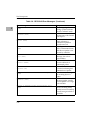
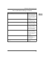
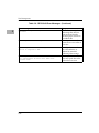


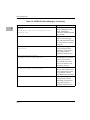
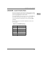


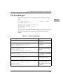
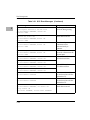
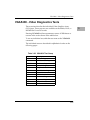


![Fio 2.0 UM ECU [ENG]](http://vs1.manualzilla.com/store/data/005638068_1-6dee15c8bb797972f1fa6aeeeee54189-150x150.png)