1
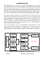
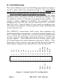
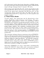
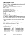
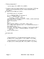
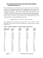
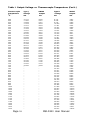
MSI-P440 8-CHANNEL THERMOCOUPLE & 8-CHANNEL 12-BIT A/D CARD USER MANUAL Revised 10-25-2013 PC/104 Embedded Industrial Analog I/O Series Microcomputer Systems, Inc. 1814 Ryder Drive ¨ Baton Rouge, LA 70808 Ph (225) 769-2154 ¨ Fax (225) 769-2155 Email: [email protected] http://www.microcomputersystems.com Page MSI-P440 User Manual CONTENTS I. INTRODUCTION 3 II. HARDWARE DESCRIPTION 5 A. Card Configuration B. Card Addressing C. Interrupt Connections D. Connecting Inputs to J1. III. PROGRAMMING 9 A. Control Register Format B. Performing a Conversion C. Reading the Data Register D. Input Data Formats E. Power-Down Modes F. Example BASIC Program G. Example 'C' Program Sequence IV. Temperature vs Thermocouple Input Voltage (Channels 0 thru 7) 15 V. SPECIFICATIONS 17 APPENDIX 17 Circuit Diagram of MSI-P440 See P440-1.pdf and P440-2.pdf Page MSI-P440 User Manual I. INTRODUCTION The MSI-P440 is a low cost, high performance card that provides eight thermocouple inputs and eight 12-bit analog inputs designed for use with all PC/104 embedded systems. Two models provide selections of (a) eight K type thermocouple inputs, or (b) eight K type thermocouple and eight 12-bit channels of analog inputs. Software programmable input ranges are 0-5V, 0-10V, ±5V and ±10V with a linearity of 1/2 LSB. The thermocouple inputs are conditioned by Analog Devices AD597 devices which provide built-in ice point compensation with temperature proportional operation of 10 mV/°C. The analog inputs are single-ended with an input impedance of 1MΩ. In addition, a fault condition on any channel will not effect the conversion result on the selected channel. A block diagram of the card is shown below. The card employs up to two MAX197 eight-channel A/D converters that incorporate a precision 2.5V reference source with buffer amp, an internal 1.56 MHz clock, and successive approximation and internal input track/hold circuitry to PC/104 8-BIT STACKTHROUGH CONNECTOR A4-A15 JUMPERS PC/104 BUS INTERFACE NETWORK AD597 THERMOCOUPLE CONDITIONERS 16-PIN OR 34-PIN CONNECTOR (CH 0-7) MAX197 (CH 0-7) MSI-P440 PC/104 BUS INTERRUPT NETWORK INTERRUPT JUMPERS MAX197 (CH 8-15) INPUT BUFFER AMPLIFIERS 16-PIN OR 34-PIN CONNECTOR (CH 8-15) Figure 1. Block Diagram of the MSI-P440. Page 3 MSI-P440 User Manual convert the analog signal of each channel into a 12-bit digital signal. Low span and offset errors result in no adjustments being required for these functions. Typical total conversion times of 12 us gives a sample rate of 83 ksps for each group times of 12 us gives a sample rate of 83 ksps for each group of eight channels yielding rates up to 166 ksps for 16 input channels. The card is I/O mapped using 16-bit addressing to select the input channels and device status. Option jumpers are provided by JP1 for specifying the card address (A4 - A15) and interrupt processing is provided for IRQ4 thru IRQ7 and IRQ9 using options jumpers, as described in the next section. Page 4 MSI-P440 User Manual II. HARDWARE DESCRIPTION A. Card Configuration The MSI-C440 card is a CMOS design using through-hole and surface-mounted devices. The card configuration is shown in Figure 2 and a circuit diagram of the network is given in the Appendix. Thermocouple input signals for channels 0 thru 7 are applied to connector J1, pins 1 thru 16. Analog input channels 8 thru 15 are applied to connector J1, pins 17 thru 34. Jumper block JP1 is used for address selection (Pins 1 thru 24) and interrupt configuration (Pins 25 thru 34), as described below. Figure 2. MSI-P440 card outline. Page 5 MSI-P440 User Manual B. Card Addressing The card address is set by installing appropriate jumpers on JP1, pins 1 thru 24, as shown in Fig. 3. An uninstalled jumper for a given address bit sets the bit to 1 (true) and an installed jumper sets the bit equal to 0 (false). Addresses A4 thru A15 are jumper selectable for defining the base address of the card from 0000H to FFF0H on integral 10H boundaries, where H denotes a hexadecimal number. To assign a base address of 3040H, for example, install jumpers JP1-A4, JP1-A5, JP1-A7 thru JP1-A11, JP1-A14 and JP1-A15. Pins 25 thru 34 are used to configure the interrupt connections, if interrupts are used, as described in the Section II.C. A15 A14 A13 A12 A11 A10 A9 A8 A7 A6 A5 A4 INT IN ENABLE INT OUT 1 KOhm IRQ9 2 4 6 8 10 12 14 16 18 20 22 24 26 28 30 32 34 o o o o o o o o o o o o o o o o o o o o o o o o o o o o o o o o o o 1 3 5 7 9 11 13 15 17 19 21 23 25 27 33 IRQ5 INT OUT 29 31 IRQ4 IRQ6 IRQ7 The MAX197 converters each have two registers for performing data conversions, a control output register (C) and a input data register (I). A third register implemented on the card for denoting interrupt status is called the status register. The addresses of the control, input data (C/I) and status for each channel is given in Table 1. The functions of the control, the input data (hi and lo bytes), and status registers are described in the Section III. Figure 3. Jumper block JP1 configuration. Page 6 MSI-P440 User Manual Table 1. Analog Converter Control Register Addresses Channels Control Output (C) Data Input (I) Status / Bit 0-7 base+0 base+0 (lo) base+1 (hi) base+8 / 0 8-15 base+2 base+2 (lo) base+3 (hi) base+8 / 1 C. Interrupt Connections Interrupt connections are implemented by pins 25 thru 34 of JP1. The steps in the procedure are as follows. 1) Pin 30 (INT OUT) is the composite interrupt signal from the analog converters (see circuit diagram in Appendix). This is jumpered to a single desired interrupt, IRQ4 thru IRQ9, of JP1 shown in Fig. 3. This connection causes the interrupt selected to be activated when a conversion is performed. 2) If no other cards in the system are using the interrupt line chosen in step 1, proceed to step 3. Pin 26 of JP1 (INT IN) is used to control the tri-state buffer of INT OUT when other cards are using the same interrupt line chosen in step 1. In this case, connect pins 26 and 28 of JP1. This results in the tri-state buffer of INT OUT being enabled only when an interrupt request is active. The status is then checked to determine which interrupt is active, as described in Section III. 3) Pin 32 of JP1 (1 KOhm pull-down resistor) is used to properly terminate the interrupt line selected in step 1. This pin should be jumpered to the interrupt line on only one card in the system. D. Connecting Inputs to J1. Thermocouple inputs are interconnected to the card via J1 using a flat cable connector. Pin assignments are given in Table 2a. Page 7 MSI-P440 User Manual Table 2a. Connector J1 Thermocouple Inputs. Input Pin Input Pin T/C 0 T/C 0+ J1-16 J1-15 T/C 4 T/C 4+ J1-8 J1-7 T/C 1 T/C 1+ J1-14 J1-13 T/C 5 T/C 5+ J1-6 J1-5 T/C 2 T/C 2+ J1-12 J1-11 T/C 6 T/C 5+ J1-4 J1-3 T/C 3 T/C 3+ J1-10 J1-9 T/C 7 T/C 7+ J1-2 J1-1 The analog inputs are interconnected to the card via J1 using a flat cable connector. Pin assignments are given in Table 2b. Table 2a. Connector J1 Analog Inputs. Input Pin Input Pin GND +5V* CH 8CH 8+ J1-33 J1-34 J1-32 J1-31 CH 12- J1-24 CH 12+ J1-23 CH 9CH 9+ J1-30 J1-29 CH 13- J1-22 CH 13+ J1-21 CH 10CH 10+ J1-28 J1-27 CH 14- J1-20 CH 14+ J1-19 CH 11CH 11+ J1-26 J1-25 CH 15- J1-18 CH 15+ J1-17 * Page 8 +5V is fused for 0.5A MSI-P440 User Manual III. PROGRAMMING Performing data conversions involves a write operation to the control register of the appropriate MAX197, which selects the mux channel and configures the input mode. The data is then read, lo byte and hi byte, when the conversion has been completed. A. Control Register Format The control register is an 8-bit (write-only) register that selects the mux channel and mode of the converter. The format is D7(MSB) D6 PD1 D5 PD0 ACQMOD D4 RNG D3 BIP D2 A2 D1 D0(LSB) A1 A0 where PD1, PD0 select the clock and power down mode (Table 3). ACQMOD - 0 = internally controlled acquisition, 1 = externally controlled acquisition. RNG selects the full-scale voltage range (Table 4). BIP selects unipolar or bipolar conversion mode (Table 4). A2, A1, A0 select the desired input channel 0-7 of the MAX197. PD1 0 0 1 1 Table 3. Clock and Power Down Selection PD0 DEVICE MODE 0 Normal Operation/External Clock Mode 1 Normal Operation/Internal Clock Mode 0 Standby Power-down (STBYPD); clock unaffected 1 Full Power-down (FULLPD); clock unaffected Table 4. Range and Polarity Selection BIP RNG INPUT RANGE (V) 0 0 0 to 5 0 1 0 to 10 1 0 ±5 1 1 ±10 Page 9 MSI-P440 User Manual The card is designed to operate using the internal clock with PD1 = 0 and PD0 = 1 in normal operation. The internally controlled acquisition (ACQMOD = 0) is normally used . B. Performing a Conversion Conversions are initiated with a write operation to the control register (Table 1), which selects the mux channel of the desired MAX197 (U5, Channel 0-7 or U4, Channel 815) and configures the device mode. Selecting ACQMOD = 0 in the control register selects the internal acquisition mode. This causes the write to the control register to initiate the acquisition interval whose duration is internally timed. Conversion starts when this six-clock-cycle acquisition interval ends. Writing a new control byte during the conversion cycle will abort the conversion and start a new acquisition interval. C. Reading the Data Register Conversions are complete when the appropriate status bit (Table 1) becomes 0 following a write to the control register. Channels 0-7 (U5), for example, are ready when bit 0 at address base+8 is 0. The data can now be read at the appropriate lo and hi byte addresses for the lo and hi bytes of the channel selected (A2, A1, A0 of the control register). In the case of channels 0-7, addresses base+0 and base+1, respectively, are read. D. Input Data Format Unipolar Mode - the output data format is binary. In this case, 0 volts input yields 000H, where H denotes a hexadecimal number. The value increases linearly from 000H to FFFH with increasing input voltage. A +FS input (full-scale +5V or +10V ranges) gives FFFH. Bipolar Mode - the output data format is twos-complement binary. In this case, a -FS input (±5V or ±10V ranges) yields 800H. The value increases linearly from 800H toward FFFH as the input voltage changes from -FS toward 0 volts. Page 10 MSI-P440 User Manual At 0 volts input (in the ideal case), the value is 000H. Again, the value increases linearly from 000H toward 7FFH as the input voltage changes from 0 toward +FS volts. The lo byte read, bits D0 thru D7, of the input data is the low byte B0 thru B7 of the conversion result. The hi byte read of the input data contains bits B8 thru B11 of the conversion result in bits D0 thru D3. Bits D4 thru D7 contain all 0's and all 1's, respectively, for the unipolar and bipolar modes. E. Power-Down Modes To save power, the converters can be placed into a lowpower shutdown mode between conversions. Two programmable power-down modes are available. Select STDBYPD or FULLPD by programming PD0 and PD1 in the control register. When software power-down is asserted, it becomes effective only after the end of conversion. In both power-down modes, the interface remains active and conversion results may be read. Input overvoltage protection is active. The converter returns to normal operation on the first write to the control register. In STDBYPD each device typically consumes 700uA and in FULLPD 120 uA maximum. The converter voltage reference remains active in STDBYPD. This is a DC power state that does not degrade after powerdown of any duration and any sampling rate can be used without regard to start-up delays. In FULLPD, however, start-up delays will effect the conversion. It is recommended when using this mode that a STDBYPD powerdown cycle be performed prior to starting conversions to allow the reference voltage to stabilize. Selecting STDBYPD on every conversion automatically shuts the MAX197 down after each conversion without requiring any start-up time on the next conversion. Page 11 MSI-P440 User Manual F. Example BASIC Program A simple BASIC program that continually inputs channels 0 thru 7 for the 5V unipolar mode and lists the results to the console is given below. 10 BASEADDR=&H300 'insert jumpers A4 thru A7, A10 thru A15 20 CBYTE = &H40 ‘Control Byte for 5V Unipolar Mode 30 FOR I = 0 TO 7 40 OUT BASEADDR,CBYTE+I ‘Write Control Byte 50 WHILE (INP(BASEADDR+8) AND 1)=1:WEND ‘Test Status 60 X=INP(BASEADDR) ‘Read LO Byte 70 Y=INP(BASEADDR+1) ‘Read HI Byte 80 X=X+256*(Y AND &HF) 'Mask off 4 MSB's of HI Byte 90 ‘Print CH0-CH4, Linefeed, CH4-CH7 100 IF I=3 OR I=7 THEN PRINT HEX$(X) ELSE PRINT HEX$(X), 110 NEXT 120 PRINT” “ 130 GOTO 30 'Go Again G. Example 'C' Program Sequence For a simple 'C' program illustration using software polling of the device status, consider a case with the following parameters and events. 1) A base address for the card of 7FF0H (insert jumper A15). 2) Read A/D channel 3 (input to U5) in the +5V unipolar mode and store the result in CH_3_INPUT. 3) Read A/D channel 9 (input to U4) in the ±10V bipolar mode and store the result in CH_9_INPUT. A simple program sequence for this operation is /* Constant declarations */ #define base_address #define control_byte_5 #define control_byte_5B #define control_byte_10 #define control_byte_10B #define delay_count Page 12 0x7ff0 0x40 0x48 0x50 0x58 1000 /* card base address */ /* control byte for +5V range */ /* control byte for ±5V range */ /* control byte for +10V range */ /* control byte for ±10V range */ /* delay count for converter time-out */ MSI-P440 User Manual /* Memory assignments */ int A_D_value, CH_3_INPUT, CH_9_INPUT; /* Routine to input A/D channel CHAN(0-15) for control byte C_BYTE and returns 0 on a converter time-out error. Stores converted value in A_D_value */ int input_A_D( int CHAN, int C_BYTE ) { int converter_error, a, i, ch_group; if( 0 <= CHAN && CHAN < 8 ) ch_group =0; else if( 7 < CHAN && CHAN < 16 ) {ch_group = 2; CHAN = CHAN - 8;} outp( base_address+ch_group, C_BYTE + CHAN ); //write control byte if( ch_group < 1 ) a = 1; //Ch 0-7 else a = 2; //Ch 8-15 i=0; do ++i; while ( (inp(base_address + 8) & a) && i < delay_count ); if( i == delay_count ) converter_error = 1;/* converter time-out error */ else converter_error = 0; A_D_value = inp( base_address + ch_group ); /* get converter value */ A_D_value = A_D_value + ((inp(base_address + ch_group + 1) & 0xf)<<8); return( converter_error ); } void main( void) { . . /* Input channel 3 for +5V range and store if no time_out error */ if( !input_A_D( 3, control_byte_5 ) ) CH_3_INPUT = A_D_value;; /* Input channel 9 for ±10V range and store if no time_out error */ if( !input_A_D( 9, control_byte_10B) ) CH_9_INPUT = A_D_value;; . . } Page 13 MSI-P440 User Manual The function input_A_D( int CHAN, int C_BYTE ) above is written in general terms to permit calls from the main routine or from other user defined functions by simply using the appropriate CHAN and C_BYTE values for the input channel desired and the desired input range. Page 14 MSI-P440 User Manual IV. Temperature vs Thermocouple Input Voltage (Channels 0 thru 7) The temperature of a thermocouple input on any of channels 0 thru 7 is determined from the voltage that is read on its associated channel. In the case of a K type thermocouple, the voltage varies from -1446 mV to 12428 mV for temperatures of -200°C to 1250°C, respectively. Table 5 gives the temperature vs voltage outputs for both J type and K type thermocouples. In the case of both J type and K type thermocouples, the temperature is approximately given by Temperature °C ≈ 100 x (Vin in Volts) The appropriate converter span (0-5V, ±5V, 0-10V or ±10V) should to be chosen for the temperature range that is being monitored. Table I. Output Voltage vs. Thermocouple Temperature Thermocouple Temperature °C Type J Voltage mV AD596 Output mV Type K Voltage mV AD597 Output mV –200 –180 –160 –140 –120 –100 –80 –60 –40 –20 –10 0 10 20 25 30 40 50 60 80 100 120 140 160 180 –7.890 –7.402 –6.821 –6.159 –5.426 –4.632 –3.785 –2.892 –1.960 –.995 –.501 0 .507 1.019 1.277 1.536 2.058 2.585 3.115 4.186 5.268 6.359 7.457 8.560 9.667 –1370 –1282 –1177 –1058 –925 –782 –629 –468 –299 –125 –36 54 146 238 285 332 426 521 617 810 1006 1203 1401 1600 1800 –5.891 –5.550 –5.141 –4.669 –4.138 –3.553 –2.920 –2.243 –1.527 –.777 –.392 0 .397 .798 1.000 1.203 1.611 2.022 2.436 3.266 4.095 4.919 5.733 6.539 7.338 –1446 –1362 –1262 –1146 –1016 –872 –717 –551 –375 –191 –96 0 97 196 245 295 395 496 598 802 1005 1207 1407 1605 1801 Page 15 MSI-P440 User Manual Table I. Output Voltage vs. Thermocouple Temperature (Con’t.) Thermocouple Temperature Type J Voltage °C mV 200 220 240 260 280 300 320 340 360 380 400 420 440 460 480 500 520 540 560 580 600 620 640 660 680 700 720 740 750 760 780 800 820 840 860 880 900 920 940 960 980 1000 1020 1040 1060 1080 1100 1120 1140 1160 1180 1200 1220 1240 10.777 11.887 12.998 14.108 15.217 16.325 17.432 18.537 19.640 20.743 21.846 22.949 24.054 25.161 26.272 27.388 28.511 29.642 30.782 31.933 33.096 34.273 35.464 36.671 37.893 39.130 40.382 41.647 42.283 – – – – – – – – – – – – – – – – – – – – – – – – – 1250 – Page 16 AD596 Output Type K Voltage AD597 Output mV mV 2000 2201 2401 2602 2802 3002 3202 3402 3601 3800 3999 4198 4398 4598 4798 5000 5203 5407 5613 5821 6031 6243 6458 6676 6897 7120 7346 7575 7689 – – – – – – – – – – – – – – – – – – – – – – – – – 8.137 8.938 9.745 10.560 11.381 12.207 13.039 13.874 14.712 15.552 16.395 17.241 18.088 18.938 19.788 20.640 21.493 22.346 23.198 24.050 24.902 25.751 26.599 27.445 28.288 29.128 29.965 30.799 31.214 31.629 32.455 33.277 34.095 34.909 35.718 36.524 37.325 38.122 38.915 39.703 40.488 41.269 42.045 42.817 43.585 44.439 45.108 45.863 46.612 47.356 48.095 48.828 49.555 50.276 1997 2194 2392 2592 2794 2996 3201 3406 3611 3817 4024 4232 4440 4649 4857 5066 5276 5485 5694 5903 6112 6321 6529 6737 6944 7150 7355 7560 7662 7764 7966 8168 8369 8569 8767 8965 9162 9357 9552 9745 9938 10130 10320 10510 10698 10908 11072 11258 11441 11624 11805 11985 12164 12341 – 50.633 12428 mV MSI-P440 User Manual V. SPECIFICATIONS PC/104 Analog Inputs Channels Converter Thermocouple I/F Analog Input Ranges Resolution Conversion Rate Non-linearity Offset Error Gain Error Signal-to-Noise Input Resistance Internal Reference Ref Out Voltage Temp. Coeff. Connectors J1 (MSI-P440-K/A) J1 (MSI-P440-K) Interrupts Channels 8-bit, stackthrough 8 to 16 in groups of 8 MAXIM MAX197 Analog Devices AD597 (K type) 0-5V, 0-10V, ±5V, ±10V (Single-ended) 12 bits 82 ksps per 8 channels ±1/2 LSB < 0.5% of Span < 0.5% of Span 70 dB min 1 MΩ (Analog Input Channels) 4.096 V ±1.5% max. 40 ppm/°C One (1) 30334-5502 or eq. (34-pin) One (1) 30316-5502 or eq. (16-pin) One, sharing with tri-state buffer for IRQ4-7, 9 Option Jumpers .025" square posts, 0.1" grid Electrical & Environmental +5V @ 50 mA typical -40° to 85° C APPENDIX Circuit Diagrams See P440-1.pdf and P440-2.pdf Page 17 MSI-P440 User Manual