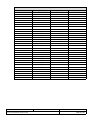
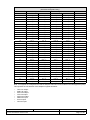
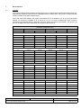
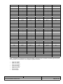
1
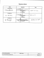
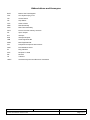
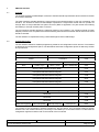
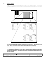
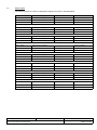
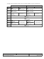
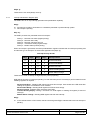
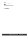
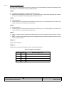
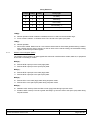
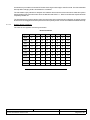
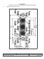
CCII Systems (Pty) Ltd Registration No. 1990/005058/07
C ommunications
C omputer I ntellig ence
I nteg ration
User Manual
for
C²I² Systems
8-Channel Serial I/O PMC Adapter
C²I² Systems Document No.
CCII/LCP/6-MAN/003
Document Issue
1.1
Issue Date
2003-10-29
Print Date
2003-10-29
File Name
W:\LCP\TECH\MAN\CLCMAN03.WPD
Distribution List No
© C²I² Systems The copyright of this document is the property of C²I² Systems. The document is issued for the sole
purpose for which it is supplied, on the express terms that it may not be copied in whole or part, used by
or disclosed to others except as authorised in writing by C²I² Systems.
Document prepared by and for C²I² Systems, Cape Town
Amendment History
Issue
Description
Date
ECP No.
0.1
First draft
2002-07-03
-
1.0
Updated to new template
2003-07-16
-
1.1
Added Ordering Information and Part Number of the Molex
Front Panel Connector, Mating Connector and Ribbon Cable
2003-10-29
CCII/LCP/6-ECP/009
CCII/LCP/6-MAN/003
W:\LCP\TECH\MAN\CLCMAN03.WPD
2003-10-29
Issue 1.1
Page iii of v
Contents
1.
Introduction and Scope . . . . . . . . . . . . . . . . . . . . . . . . . . . . . . . . . . . . . . . . . . . . . . . . . . . . . 1
1.1
1.2
1.3
2.
Applicable and Reference Documents . . . . . . . . . . . . . . . . . . . . . . . . . . . . . . . . . . . . . . . . . 2
2.1
2.2
2.3
3.
Applicable Documents . . . . . . . . . . . . . . . . . . . . . . . . . . . . . . . . . . . . . . . . . . . . . . . . . . . . . . . . . . . . . . . . . 2
Reference Documents . . . . . . . . . . . . . . . . . . . . . . . . . . . . . . . . . . . . . . . . . . . . . . . . . . . . . . . . . . . . . . . . . 2
Specifications . . . . . . . . . . . . . . . . . . . . . . . . . . . . . . . . . . . . . . . . . . . . . . . . . . . . . . . . . . . . . . . . . . . . . . . . 2
PMC/PCI Interface . . . . . . . . . . . . . . . . . . . . . . . . . . . . . . . . . . . . . . . . . . . . . . . . . . . . . . . . . 3
3.1
3.2
3.3
3.4
3.5
4.
Scope . . . . . . . . . . . . . . . . . . . . . . . . . . . . . . . . . . . . . . . . . . . . . . . . . . . . . . . . . . . . . . . . . . . . . . . . . . . . . . 1
Introduction . . . . . . . . . . . . . . . . . . . . . . . . . . . . . . . . . . . . . . . . . . . . . . . . . . . . . . . . . . . . . . . . . . . . . . . . . 1
System Overview . . . . . . . . . . . . . . . . . . . . . . . . . . . . . . . . . . . . . . . . . . . . . . . . . . . . . . . . . . . . . . . . . . . . . 1
Overview . . . . . . . . . . . . . . . . . . . . . . . . . . . . . . . . . . . . . . . . . . . . . . . . . . . . . . . . . . . . . . . . . . . . . . . . . . . 3
Configuration Space . . . . . . . . . . . . . . . . . . . . . . . . . . . . . . . . . . . . . . . . . . . . . . . . . . . . . . . . . . . . . . . . . . 3
PCI Interrupts . . . . . . . . . . . . . . . . . . . . . . . . . . . . . . . . . . . . . . . . . . . . . . . . . . . . . . . . . . . . . . . . . . . . . . . . 4
PMC Connectors . . . . . . . . . . . . . . . . . . . . . . . . . . . . . . . . . . . . . . . . . . . . . . . . . . . . . . . . . . . . . . . . . . . . . 4
PMC Pin Assignments . . . . . . . . . . . . . . . . . . . . . . . . . . . . . . . . . . . . . . . . . . . . . . . . . . . . . . . . . . . . . . . . . 5
Serial Interface . . . . . . . . . . . . . . . . . . . . . . . . . . . . . . . . . . . . . . . . . . . . . . . . . . . . . . . . . . . . 8
4.1
4.2
4.3
4.4
Overview . . . . . . . . . . . . . . . . . . . . . . . . . . . . . . . . . . . . . . . . . . . . . . . . . . . . . . . . . . . . . . . . . . . . . . . . . . . 8
Line Driver Selection . . . . . . . . . . . . . . . . . . . . . . . . . . . . . . . . . . . . . . . . . . . . . . . . . . . . . . . . . . . . . . . . . 10
Memory Map . . . . . . . . . . . . . . . . . . . . . . . . . . . . . . . . . . . . . . . . . . . . . . . . . . . . . . . . . . . . . . . . . . . . . . . 11
UART Register Description . . . . . . . . . . . . . . . . . . . . . . . . . . . . . . . . . . . . . . . . . . . . . . . . . . . . . . . . . . . . 13
4.4.1 Transmitter Holding Register (THR) . . . . . . . . . . . . . . . . . . . . . . . . . . . . . . . . . . . . . . . . . . . . . . . 13
4.4.2 Receive Holding Register (RHR) . . . . . . . . . . . . . . . . . . . . . . . . . . . . . . . . . . . . . . . . . . . . . . . . . 13
4.4.3 Interrupt Enable Register (IER) . . . . . . . . . . . . . . . . . . . . . . . . . . . . . . . . . . . . . . . . . . . . . . . . . . 13
4.4.4 Interrupt Identification Register (IIR) . . . . . . . . . . . . . . . . . . . . . . . . . . . . . . . . . . . . . . . . . . . . . . . 14
4.4.5 FIFO Control Register (FCR) . . . . . . . . . . . . . . . . . . . . . . . . . . . . . . . . . . . . . . . . . . . . . . . . . . . . 16
4.4.6 Line Control Register (LCR) . . . . . . . . . . . . . . . . . . . . . . . . . . . . . . . . . . . . . . . . . . . . . . . . . . . . . 17
4.4.7 Modem Control Register (MCR) . . . . . . . . . . . . . . . . . . . . . . . . . . . . . . . . . . . . . . . . . . . . . . . . . . 18
4.4.8 Line Status Register (LSR) . . . . . . . . . . . . . . . . . . . . . . . . . . . . . . . . . . . . . . . . . . . . . . . . . . . . . . 19
4.4.9 Modem Status Register (MSR) . . . . . . . . . . . . . . . . . . . . . . . . . . . . . . . . . . . . . . . . . . . . . . . . . . . 20
4.4.10 Scratch Pad Register (SPR) . . . . . . . . . . . . . . . . . . . . . . . . . . . . . . . . . . . . . . . . . . . . . . . . . . . . . 21
4.4.11 Programmable Baud-Rate Generator . . . . . . . . . . . . . . . . . . . . . . . . . . . . . . . . . . . . . . . . . . . . . . 22
4.4.12 FIFO Interrupt Mode Operation . . . . . . . . . . . . . . . . . . . . . . . . . . . . . . . . . . . . . . . . . . . . . . . . . . 22
4.4.13 Register Reset Conditions . . . . . . . . . . . . . . . . . . . . . . . . . . . . . . . . . . . . . . . . . . . . . . . . . . . . . . 23
Appendix A . . . . . . . . . . . . . . . . . . . . . . . . . . . . . . . . . . . . . . . . . . . . . . . . . . . . . . . . . . . . . . . . . 24
MOLEX Connector Pin Locations and Ordering Information . . . . . . . . . . . . . . . . . . . . . . . . . . . . . . . . . . . . . . . . . 24
CCII/LCP/6-MAN/003
W:\LCP\TECH\MAN\CLCMAN03.WPD
2003-10-29
Issue 1.1
Page iv of v
Abbreviations and Acronyms
BIST
CCII
Built In Self Test Register
CCII Systems (Pty) LTD
CD
Carrier Detect
CS
Chip Select
CTS
Clear to Send
DSR
Data Set Ready
DTR
Data Terminal Ready
FIFO
First In First Out memory structure
I/O
Input / Output
INT
Interrupt
IRQ
Interrupt Request
LSB
Least Significant Bit
MSB
Most Significant Bit
PCI
Peripheral Component Interconnect
PMC
PCI Mezzanine Card
RI
Ring Indicator
RTS
Request To Send
RX
Receive
TX
Transmit
UART
Universal Asynchronous Receiver Transmitter
CCII/LCP/6-MAN/003
W:\LCP\TECH\MAN\CLCMAN03.WPD
2003-10-29
Issue 1.1
Page v of v
1.
Introduction and Scope
1.1
Scope
This document serves as a user manual for C²I² Systems 8-Channel Serial I/O PMC Adapter.
1.2
Introduction
The 8-Channel Serial I/O PMC Adapter provides eight full duplex, asynchronous serial ports. All eight ports are
capable of transmitting and receiving data using either RS-232 or RS-422/485 standards.
The 8-Channel Serial I/O PMC Adapter adheres to the electrical requirements of the PCI interface specification
and to the mechanical requirements of the PMC interface standard.
1.3
System Overview
The block diagram of the adapter is shown in Figure 1.
PMC Bus
Configuration
EEPROM
(optional)
Channel 1
8-Channel
UART
with
PCI Interface
Channel 8
User Selectable
RS-232/RS-422
Level Converter
User Selectable
RS-232/RS-422
Level Converter
Serial I/O
Serial I/O
Bus Mode
PAL
Figure 1 : Block diagram of the 8-Channel Serial I/O PMC Adapter
CCII/LCP/6-MAN/003
W:\LCP\TECH\MAN\CLCMAN03.WPD
2003-10-29
Issue 1.1
Page 1 of 26
2.
Applicable and Reference Documents
2.1
Applicable Documents
None
2.2
Reference Documents
None
2.3
Specifications
2.3.1
PCI Local Bus Specification, Revision 2.1, Dated June 1, 1995
2.3.2
Draft Standard Physical and Environmental Layers for PCI Mezzanine Cards : PMC, P1386.1/Draft 2.0,
Dated April 4, 1995
2.3.3
Draft Standard for a Common Mezzanine Card Family : CMC, P1386/Draft 2.0, Dated April 4, 1995
CCII/LCP/6-MAN/003
W:\LCP\TECH\MAN\CLCMAN03.WPD
2003-10-29
Issue 1.1
Page 2 of 26
3.
PMC/PCI Interface
3.1
Overview
The 8-Channel Serial I/O PMC Adapter conforms to the PMC interface specification which is based on the PCI
bus interface standard.
The PMC interface standard defines the physical and environmental aspects of the PCI mezzanine card
interface. The 8-Channel Serial I/O PMC Adapter implements a single width module that can provide I/O
through either a 120 pin MOLEX front panel connector (Refer to Appendix A for part number and ordering
information) or through the back plane connector.
The PCI interface standard defines the electrical aspects of the interface. The 8-Channel Serial I/O PMC
Adapter provides a PCI compliant slave interface allowing the host board to transfer data to and from the serial
interface controller.
The PCI interface is implemented using a PCI based eight-channel UART bridge.
3.2
Configuration Space
The PCI interface defines a standard programming model for the configuration of PCI devices. This interface
is defined as the Configuration Space. The table below shows the Configuration Space as defined by the PCI
bus specification :
AD31-23
AD22-16
AD15-8
AD7-0
Address
Device ID(0x0158)
Vendor ID(0x13AB)
0x00
Status
Command
0x04
Class Code(0x070002)
BIST
Header Type
Latency Timer
0x08
Cache Size(0x00)
0x0C
Memory Base Address Register (BAR)
0x10
Unimplemented Base Address Register
0x14
Unimplemented Base Address Register
0x18
Unimplemented Base Address Register
0x1C
Unimplemented Base Address Register
0x20
Unimplemented Base Address Register
0x24
Reserved
0x28
Subsystem ID
Max Latency(0x00)
Revision ID(0x01)
Subsystem Vendor ID
0x2C
Reserved
0x30
Reserved
0x34
Reserved
0x38
Min Grant(0x00)
Interrupt Pin(0x01)
Interrupt Line
0x3C
The location of the configuration registers is defined by the host board. The host board assigns a specific
address line to the module interface by connecting it to the IDSEL pin on the PMC interface. To determine the
configuration registers locations refer to the manual of the host board.
CCII/LCP/6-MAN/003
W:\LCP\TECH\MAN\CLCMAN03.WPD
2003-10-29
Issue 1.1
Page 3 of 26
3.3
PCI Interrupts
The 8-Channel Serial I/O PMC Adapter supports interrupts on the INTA# pin only. This is reflected in the
Interrupt Pin Register of the Configuration Space as defined in 3.2.
3.4
PMC Connectors
The 8-Channel Serial I/O PMC Adapter is fitted with two connectors (P11 and P12) to implement the
32-bit PMC interface. The board may be fitted with a either connector P14 (required for back plane connection
to the interface signals) or the front panel connector (J2). The front and rear panel configurations are shown
in Figure 2 and Figure 3 respectively.
J2
P11 P12
Figure 2 : Front panel I/O Configuration
P14
P11 P12
Figure 3 : Rear Panel I/O Configuration
CCII/LCP/6-MAN/003
W:\LCP\TECH\MAN\CLCMAN03.WPD
2003-10-29
Issue 1.1
Page 4 of 26
3.5
PMC Pin Assignments
The 8-Channel Serial I/O PMC Adapter has the following PMC connections (note that P14 is only for the rear
panel configuration) :
P11 Signals
Pin
Signal Name
Signal Name
Pin
1
TCK
-12V
2
3
Ground
INTA#
4
5
INTB#
INTC#
6
7
BUSMODE1#
+5V
8
9
INTD#
PCI-RSVD
10
11
Ground
PCI-RSVD
12
13
CLK
Ground
14
15
Ground
GNT#
16
17
REQ#
+5V
18
19
V (I/O)
AD[31]
20
21
AD[28]
AD[27]
22
23
AD[25]
Ground
24
25
Ground
C/BE[3]#
26
27
D[22]
AD[21]
28
29
AD[19]
+5V
30
31
V (I/O)
AD[17]
32
33
FRAME#
Ground
34
35
Ground
IRDY#
36
37
DEVSEL#
+5V
38
39
Ground
LOCK#
40
41
SDONE#
SBO#
42
43
PAR
Ground
44
45
V (I/O)
AD[15]
46
47
AD[12]
AD[11]
48
49
AD[09]
+5V
50
51
Ground
C/BE[0]#
52
53
AD[06]
AD[05]
54
55
AD[04]
Ground
56
57
V (I/O)
AD[03]
58
59
AD[02]
AD[01]
60
61
AD[00]
+5V
62
63
Ground
REQ64#
64
CCII/LCP/6-MAN/003
W:\LCP\TECH\MAN\CLCMAN03.WPD
2003-10-29
Issue 1.1
Page 5 of 26
P12 Signals
Pin
Signal Name
Signal Name
Pin
1
+12V
TRST#
2
3
TMS
TDO
4
5
TDI
Ground
6
7
Ground
PCI-RSVD
8
9
PCI-RSVD
PCI-RSVD
10
11
BUSMODE2#
+3.3V
12
13
RST#
BUSMODE3#
14
15
+3.3V
BUSMODE4#
16
17
PCI-RSVD
Ground
18
19
AD[30]
AD[29]
20
21
Ground
AD[26]
22
23
AD[24]
+3.3V
24
25
IDSEL
AD[23]
26
27
+3.3V
AD[20]
28
29
AD[18]
Ground
30
31
AD[16]
C/BE[2]#
32
33
Ground
PMC-RSVD
34
35
TRDY#
+3.3V
36
37
Ground
STOP#
38
39
PERR#
Ground
40
41
+3.3V
SERR#
42
43
C/BE[1]#
Ground
44
45
AD[14]
AD[13]
46
47
Ground
AD[10]
48
49
AD[08]
+3.3V
50
51
AD[07]
PMC-RSVD
52
53
+3.3V
PMC-RSVD
54
55
PMC-RSVD
Ground
56
57
PMC-RSVD
PMC-RSVD
58
59
Ground
PMC-RSVD
60
61
ACK64#
+3.3V
62
63
Ground
PMC-RSVD
64
CCII/LCP/6-MAN/003
W:\LCP\TECH\MAN\CLCMAN03.WPD
2003-10-29
Issue 1.1
Page 6 of 26
P14 Signals
( Rear Panel Configuration Only )
Pin
Signal Name
RS-232
Signal Name
RS-422
RS-232
Pin
RS-422
1
TX_A
TX+_A
RTS_A
TX-_A
2
3
DTR_A
RTS+_A
RX_A
RTS-_A
4
5
CTS_A
RX+_A
DSR_A
RX-_A
6
7
CD_A
CTS+_A
RI_A
CTS-_A
8
9
TX_A
TX+_A
RTS_A
TX-_A
10
11
DTR_B
RTS+_B
RX_B
RTS-_B
12
13
CTS_B
RX+_B
DSR_B
RX-_B
14
15
CD_B
CTS+_B
RI_B
CTS-_B
16
17
TX_C
TX+_C
RTS_C
TX-_C
18
19
DTR_C
RTS+_C
RX_C
RTS-_C
20
21
CTS_C
RX+_C
DSR_C
RX-_C
22
23
CD_C
CTS+_C
RI_C
CTS-_C
24
25
TX_D
TX+_D
RTS_D
TX-_D
26
27
DTR_D
RTS+_D
RX_D
RTS-_D
28
29
CTS_D
RX+_D
DSR_D
RX-_D
30
31
CD_D
CTS+_D
RI_D
CTS-_D
32
33
TX_E
TX+_E
RTS_E
TX-_E
34
35
DTR_E
RTS+_E
RX_E
RTS-_E
36
37
CTS_E
RX+_E
DSR_E
RX-_E
38
39
CD_E
CTS+_E
RI_E
CTS-_E
40
41
TX_F
TX+_F
RTS_F
TX-_F
42
43
DTR_F
RTS+_F
RX_F
RTS-_F
44
45
CTS_F
RX+_F
DSR_F
RX-_F
46
47
CD_F
CTS+_F
RI_F
CTS-_F
48
49
TX_G
TX+_G
RTS_G
TX-_G
50
51
DTR_G
RTS+_G
RX_G
RTS-_G
52
53
CTS_G
RX+_G
DSR_G
RX-_G
54
55
CD_G
CTS+_G
RI_G
CTS-_G
56
57
TX_H
TX+_H
RTS_H
TX-_H
58
59
DTR_H
RTS+_H
RX_H
RTS-_H
60
61
CTS_H
RX+_H
DSR_H
RX-_H
62
63
CD_H
CTS+_H
RI_H
CTS-_H
64
Note : P14 Signals are configured such that the adapter channels function as Data Terminal Equipment (DTE).
This specifies the I/O direction of the adapter’s signals as follows :
•
•
•
•
•
•
•
•
TxD is an output
RxD is an input
RTS is an output
CTS is an input
DTR is an output
DSR is an input
RI is an input
CD is an input
CCII/LCP/6-MAN/003
W:\LCP\TECH\MAN\CLCMAN03.WPD
2003-10-29
Issue 1.1
Page 7 of 26
4.
Serial Interface
4.1
Overview
The 8-Channel Serial I/O PMC Adapter has eight asynchronous, RS-232 or RS-422/485 switchable serial ports.
Programming registers for these ports are compatible with the 16C550 UART. Each ports is configured by DIP
switches located on the PMC Adapter board.
On the rear panel PMC Adapter, the signals are available at P14 as detailed in 3.5. On the front panel PMC
Adapter, the signals are available at J2 as shown in 3.4. J2 is a 120 pin shielded right angle connector
manufactured by MOLEX (Refer to Appendix A for part number and ordering information). The pinout is as
show in the table below (see Appendix A for the physical pin locations).
J2 Signals
( Front Panel Configuration Only )
Pin
Signal Name
RS-232
Signal Name
RS-422
RS-232
Pin
RS-422
Port A
2
TX_A
TX+_A
RTS_A
TX-_A
4
6
DTR_A
RTS+_A
RX_A
RTS-_A
8
10
CTS_A
RX+_A
DSR_A
RX-_A
12
14
CD_A
CTS+_A
RI_A
CTS-_A
16
18
DTR+_A
DTR-_A
20
22
DSR+_A
DSR-_A
24
26
CD+_A
CD-_A
28
Port B
30
TX_B
TX+_B
RTS_B
TX-_B
1
3
DTR_B
RTS+_B
RX_B
RTS-_B
5
7
CTS_B
RX+_B
DSR_B
RX-_B
9
11
CD_B
CTS+_B
RI_B
CTS-_B
13
15
DTR+_B
DTR-_B
17
19
DSR+_B
DSR-_B
21
23
CD+_B
CD-_B
25
Port C
27
TX_C
TX+_C
RTS_C
TX-_C
29
32
DTR_C
RTS+_C
RX_C
RTS-_C
34
36
CTS_C
RX+_C
DSR_C
RX-_C
38
40
CD_C
CTS+_C
RI_C
CTS-_C
42
44
DTR+_C
DTR-_C
46
48
DSR+_C
DSR-_C
50
52
CD+_C
CD-_C
54
RTS_D
TX-_D
58
Port D
56
TX_D
TX+_D
60
DTR_D
RTS+_D
RX_D
RTS-_D
31
33
CTS_D
RX+_D
DSR_D
RX-_D
35
37
CD_D
CTS+_D
RI_D
CTS-_D
39
41
DTR+_D
DTR-_D
43
45
DSR+_D
DSR-_D
47
49
CD+_D
CD-_D
51
Port E
CCII/LCP/6-MAN/003
W:\LCP\TECH\MAN\CLCMAN03.WPD
2003-10-29
Issue 1.1
Page 8 of 26
53
TX_E
TX+_E
RTS_E
TX-_E
57
DTR_E
62
CTS_E
66
CD_E
55
RTS+_E
RX_E
RTS-_E
59
RX+_E
DSR_E
RX-_E
64
CTS+_E
RI_E
CTS-_E
68
70
DTR+_E
DTR-_E
72
74
DSR+_E
DSR-_E
76
78
CD+_E
CD-_E
80
Port F
82
TX_F
TX+_F
RTS_F
TX-_F
84
86
DTR_F
RTS+_F
RX_F
RTS-_F
88
90
CTS_F
RX+_F
DSR_F
RX-_F
61
63
CD_F
CTS+_F
RI_F
CTS-_F
65
67
DTR+_F
DTR-_F
69
71
DSR+_F
DSR-_F
73
75
CD+_F
CD-_F
77
Port G
79
TX_G
TX+_G
RTS_G
TX-_G
81
83
DTR_G
RTS+_G
RX_G
RTS-_G
85
87
CTS_G
RX+_G
DSR_G
RX-_G
89
92
CD_G
CTS+_G
RI_G
CTS-_G
94
96
DTR+_G
DTR-_G
98
100
DSR+_G
DSR-_G
102
104
CD+_G
CD-_G
106
Port H
108
TX_H
TX+_H
RTS_H
TX-_H
110
112
DTR_H
RTS+_H
RX_H
RTS-_H
114
116
CTS_H
RX+_H
DSR_H
RX-_H
118
120
CD_H
CTS+_H
RI_H
CTS-_H
91
95
93
DTR+_H
DTR-_H
97
DSR+_H
DSR-_H
99
101
CD+_H
CD-_H
103
105
107
109
111
113
GROUND
GROUND
115
117
GROUND
GROUND
119
Note : J2 Signals are configured such that the adapter channels function as Data Terminal Equipment (DTE).
This specifies the I/O direction of the adapter’s signals as follows :
•
•
•
•
•
•
•
•
TxD is an output
RxD is an input
RTS is an output
CTS is an input
DTR is an output
DSR is an input
RI is an input
CD is an input
CCII/LCP/6-MAN/003
W:\LCP\TECH\MAN\CLCMAN03.WPD
2003-10-29
Issue 1.1
Page 9 of 26
4.2
Line Driver Selection
All eight channels can be individually configured to use RS-232 or RS-422/485 line drivers. This is achieved
by setting the appropriate DIP switches located on the 8-Channel Serial I/O PMC Adapter as shown in Figure
4:
P1
2
P1
1
J
2
ON
ON
ON
ON
ON
Figure 4 : DIP Switch Location
S4 is used to select between RS-232 and RS-422/485 line drivers for channels A-H. When switched to the ON
position, RS-232 line drivers are selected, otherwise RS-422/485 line drivers are selected.
S1, S2, S3 and S5 are used to switch in 100 Ω line termination resistors required for RS-422/485 receivers.
When switched to the ON position, the line termination is switched in.
It is crucial that these termination resistors NOT be switched in when RS-232 drivers have been
selected on S4 (in other words, these switches must not be in the ON position when RS-232 line drivers
have been selected).
CCII/LCP/6-MAN/003
W:\LCP\TECH\MAN\CLCMAN03.WPD
2003-10-29
Issue 1.1
Page 10 of 26
4.3
Memory Map
The memory map for the device configuration registers are given in the table below :
Offset Address
Memory Space
Read/Write
Comment
0x000 - 0x007
UART channel A registers
16C550 compatible
0x100
UART A - Read FIFO
Read-Only
64 bytes of RX FIFO
0x100
UART A - Write FIFO
Write-Only
64 bytes of TX FIFO
0x200 - 0x207
UART channel B registers
0x300
UART B - Read FIFO
Read-Only
64 bytes of RX FIFO
0x300
UART B - Write FIFO
Write-Only
64 bytes of TX FIFO
0x400 - 0x407
UART channel C registers
0x500
UART C - Read FIFO
Read-Only
64 bytes of RX FIFO
0x500
UART C - Write FIFO
Write-Only
64 bytes of TX FIFO
0x600 - 0x607
UART channel D registers
0x700
UART D - Read FIFO
Read-Only
64 bytes of RX FIFO
0x700
UART D - Write FIFO
Write-Only
64 bytes of TX FIFO
16C550 compatible
16C550 compatible
16C550 compatible
0x800 - 0x807
UART channel E registers
0x900
UART E - Read FIFO
Read-Only
64 bytes of RX FIFO
16C550 compatible
0x900
UART E - Write FIFO
Write-Only
64 bytes of TX FIFO
0xA00 - 0xA07
UART channel F registers
0xB00
UART F - Read FIFO
Read-Only
16C550 compatible
64 bytes of RX FIFO
0xB40 - 0xB7F
UART F - Write FIFO
Write-Only
64 bytes of TX FIFO
0xC00 - 0xC07
UART channel G registers
0xD00
UART G - Read FIFO
Read-Only
64 bytes of RX FIFO
0xD00
UART G - Write FIFO
Write-Only
64 bytes of TX FIFO
0xE00 - 0xE07
UART channel H registers
0xF00
UART H - Read FIFO
Read-Only
64 bytes of RX FIFO
0xF00
UART H - Write FIFO
Write-Only
64 bytes of TX FIFO
CCII/LCP/6-MAN/003
W:\LCP\TECH\MAN\CLCMAN03.WPD
2003-10-29
16C550 compatible
16C550 compatible
Issue 1.1
Page 11 of 26
The UART channel configuration registers, which are 16C550 compatible, are given in the table below :
LCR[7] = 0
LCR[7] = 1
I/O Port
Read
Write
Read
Base
RBR
Receiver Buffer
THR
Transmit Holding
DLL
Divisor Latch (LSB)
Base + 1
IER
Interrupt Enable
Base + 2
IIR
Interrupt
Identification
DLM
Divisor Latch (MSB)
FCR
FIFO Control
IIR
Interrupt
Identification
Base + 3
LCR
Line Control
Base + 4
MCR
Modem Control
Base + 5
LSR
Line Status
Base + 6
MSR
Modem Status
NOT USED
MSR
Modem Status
Base + 7
W:\LCP\TECH\MAN\CLCMAN03.WPD
FCR
FIFO Control
LSR
Line Status
NOT USED
CCII/LCP/6-MAN/003
Write
SPR
Scratch Pad
2003-10-29
Issue 1.1
Page 12 of 26
4.4
UART Register Description
4.4.1
Transmitter Holding Register (THR)
The transmitter section consists of a transmitter holding register (THR) and a transmitter shift register (TSR).
The THR is actually a 16-byte FIFO. Transmitter section control is a function of the UART line control register.
The UART THR receives data off the internal data bus and when the shift register is idle, moves it into the TSR.
The TSR serializes the data and outputs it at TX. In the 16C450 mode, if the THR is empty and the transmitter
holding register empty (THRE) interrupt is enabled (IER[1] = 1), an interrupt is generated. This interrupt is
cleared when a character is loaded into the register. In the FIFO mode, the interrupts are generated based on
the control setup in the FIFO control register.
4.4.2
Receive Holding Register (RHR)
The receiver section of the UART consists of a receiver shift register (RSR) and a receiver Holding register
(RHR). The RHR is actually a 16-byte FIFO. Timing to receive holding register is supplied by the 16x receiver
clock. Receiver section control is a function of the UART line control register. The UART RHR receives serial
data from RX. The RSR then concatenates the data and moves it into the RHR FIFO. In the 16C450 mode,
when a character is placed in the receiver holding register and the received data available interrupt is enabled
(IER[0] = 1), an interrupt is generated. This interrupt is cleared when the data is read out of the receiver holding
register. In the FIFO mode, the interrupts are generated based on the control setup in the FIFO control register.
4.4.3
Interrupt Enable Register (IER)
The interrupt enable register enables each of the five types of interrupts and INT pin response to an interrupt
generation. The interrupt enable register can also be used to disable the interrupt system by clearing IER[0..3].
The contents of this register are described below.
IER[0] :
0 = Disable the received data available interrupt.
1 = Enables the received data available interrupt.
IER[1] :
0 = Disable the transmitter holding register empty interrupt.
1 = Enable the transmitter holding register empty interrupt.
IER[2] :
0 = Disables the receiver line status interrupt.
1 = Enables the receiver line status interrupt.
IER[3] :
0 = Disables the modem status interrupt.
1 = Enables the modem status interrupt.
IER[4] :
0 = Standard 16C450/550 mode. Sleep mode is disabled.
1 = Enables sleep mode. The UART is always awake when there is a byte in the transmitter, activity on the
RX, or either Delta CTS, Delta DSR, Delta CD, Delta RI is/are set to logic "1", or when the device is in the
loopback mode.
IER[5] :
0 = Standard 16C450/550 mode. Power down mode is disabled.
1 = Enables the power down mode. Power down mode functions similar to sleep mode (except oscillator
section).
CCII/LCP/6-MAN/003
W:\LCP\TECH\MAN\CLCMAN03.WPD
2003-10-29
Issue 1.1
Page 13 of 26
IER[6..7] :
These bits are not used (always set to 0).
4.4.4
Interrupt Identification Register (IIR)
The UART has an on chip interrupt generation and prioritization capability.
IIR[0] :
0 = An interrupt is pending. Used either in a hardware prioritized or polled interrupt system.
1 = No interrupt is pending.
IIR[1..2] :
The UART provides four prioritized levels of interrupts :
Priority 1 - Receiver line status (highest priority)
Priority 2 - Receiver data ready
Priority 2 - Receiver character time-out
Priority 3 - Transmitter holding register empty
Priority 4 - Modem status (lowest priority)
When an interrupt is generated, the interrupt identification register indicates that an interrupt is pending and
encodes the type of interrupt in its three least significant bits (IIR[0..2]).
Interrupt Priority decode
IIR[3]
IIR[2]
IIR[1]
IIR[0]
Interrupt source
0
1
1
0
Receive Data Error
0
1
0
0
Receive Data Ready
1
1
0
0
Receive Time-Out
0
0
1
0
Transmit Holding Empty
0
0
0
0
Modem Status Change
These bits are used to identify the highest priority interrupt pending.
IIR[0] will be set when no interrupt is pending. To clear the interrupts it is necessary to perform reads from the
following registers as required.
Receive Data Error : Reading LSR register will clear this interrupt. User should save LSR value after
reading the register to maintain the error condition.
Receive Data Ready : Reading RHR register till FIFO becomes empty.
Receive Timeout : Reading entire characters from RHR.
Transmit Holding Empty : Writing a character into THR register or reading IIR register (if source of
interrupt).
Modem Status Change : Reading MSR register will clear this interrupt.
IIR[3] :
0 = In the 16C450 mode. In FIFO mode, this bit is set along with IIR[2] to indicate that a time-out interrupt is
pending.
CCII/LCP/6-MAN/003
W:\LCP\TECH\MAN\CLCMAN03.WPD
2003-10-29
Issue 1.1
Page 14 of 26
IIR[4] :
This bit is not used (always reset at 0).
IIR[5] :
0 = 16C450/550 mode, 16 byte FIFO mode.
1 = Enhance FIFO mode. 64 byte FIFO mode enabled.
IIR[6..7] :
0 = In the 16C450 mode.
1 = When FCR[0] is set.
CCII/LCP/6-MAN/003
W:\LCP\TECH\MAN\CLCMAN03.WPD
2003-10-29
Issue 1.1
Page 15 of 26
4.4.5
FIFO Control Register (FCR)
The FIFO control register (FCR) is a write only register. The (FCR) enables and clears the FIFO sets receive
FIFO trigger level, and selects the type of DMA signaling.
FCR[0] :
0 = 16C450 mode, disables the transmitter and receiver FIFO.
1 = Enables the transmitter and receiver FIFO. This bit must be set to 1 when other (FCR) bits are written to
or they are not programmed. Changing this bit clears the FIFO.
FCR[1] :
0 = Normal operation
1 = Clears all bytes in the receiver FIFO and resets its counter logic to 0. The shift register is not cleared. The
1 that is written to this bit position is self-clearing.
FCR[2] :
0 = Normal operation
1 = Clears all bytes in the transmit FIFO and resets its counter logic to 0. The shift register is not cleared. The
1 that is written to this bit position is self-clearing.
FCR[3] :
0 = Mode 0 : Supports single transfer DMA (16C450 mode) in which a transfer is made between Host bus
cycle.
1 = Mode 1 : Supports multi transfer DMA in which multiple transfers are made continuously until the receiver
FIFO has been emptied.
FCR[5..4] :
These bits are not used.
FCR[6..7] :
These bits are used to set the trigger level for receive FIFO interrupt.
Receive Trigger Levels (Bytes)
FCR[7]
FCR[6]
RX FIFO Trigger Level
0
0
1
0
1
4
1
0
8
1
1
14
CCII/LCP/6-MAN/003
W:\LCP\TECH\MAN\CLCMAN03.WPD
2003-10-29
Issue 1.1
Page 16 of 26
4.4.6
Line Control Register (LCR)
The system programmer controls the format of the asynchronous data communication exchange through the
line control register. In addition, the programmer is able to retrieve, inspect, and modify the contents of the line
control register; this eliminates the need for separate storage of the line characteristics in system memory.
LCR[0..1] :
These two bits specify the number of bits in each transmitted or received serial character.
Word Length
LCR[1]
LCR[0]
Word Length
0
0
5 bits
0
1
6 bits
1
0
7 bits
1
1
8 bits
LCR[2] :
This bit specifies, 1, 1-1/2, or 2 stop bits in each transmitted character. When LCR[2] is reset to 0, one stop bit
is generated in the data. When LCR[2] is set to 1, the number of stop bits generated is dependent on the word
length selected with LCR[0..1]. The receiver clocks only the first stop bit regardless of the number of stop bits
selected. The number of stop bits generated in relation to word length and LCR[2].
Stop Bits
LCR[2]
Word Length
Stop Bit(s)
0
X
1
1
5 bits
1.5
1
6 bits
2
1
7 bits
2
1
8 bits
2
LCR[3] :
0 = Parity is disabled. No parity is generated or checked.
1 = Parity bit is generated in transmitted data between the last data word bit and the first stop bit. In received
data, parity is checked.
LCR[4] :
0 = ODD parity select bit. When parity is enabled by LCR[3], a 1 in LCR[4] produces odd parity (an odd
number of 1's in the data and parity bits.
1 = Even parity select bit. When parity is enabled by LCR[3], a 1 in LCR[4] produces even parity (an even
number of 1's in the data and parity bits).
LCR[5] :
0 = Stick parity is disabled.
1 = Stick parity bit. When LCR[3..5] are set to 1 the parity bit is transmitted and checked as a 0. When LCR[3]
and LCR[5] are 1's and LCR[4] is a 0, the parity bit is transmitted and checked as 1.
CCII/LCP/6-MAN/003
W:\LCP\TECH\MAN\CLCMAN03.WPD
2003-10-29
Issue 1.1
Page 17 of 26
Parity Selection
LCR[5]
LCR[4]
LCR[3]
Parity Type
X
X
0
No Parity
0
0
1
Odd Parity
0
1
1
Even Parity
1
0
1
Forced Parity “1"
1
1
1
Forced Parity “0"
LCR[6] :
0 = Normal operation. Break condition is disabled and has no effect on the transmitter logic.
1 = Force a break condition. A condition where TX is forced to the space (low) state.
LCR[7] :
0 = Normal operation.
1 = Divisor latch enable. Must be set to 1 to access the divisor latches of the baud generator during a read or
write. LCR[7] must be reset to 0 during a read or write to the receiver holding, the transmitter holding
register, or the interrupt enable register.
4.4.7
Modem Control Register (MCR)
The modem control register is an 8-bit register that controls an interface with a modem, data set, or peripheral
device that is emulating a modem.
MCR[0] :
0 = Sets the DTR output pin to the mark (high) state.
1 = Sets the DTR output pin to the space (low) state.
MCR[1] :
0 = Sets the RTS output pin to the mark (high) state.
1 = Sets the RTS output pin to the space (low) state.
MCR[2] :
0 = Sets the OP1 to the mark (high) state during loop-back mode.
1 = Sets the OP1 to the space (low) state during loop-back mode.
MCR[3] :
0 = Disables UART interrupt. Sets the OP2 to mark (high) state during loop-back mode.
1 = Enables UART interrupt. This bit is gated with IER[0..3]. Sets the OP2 to the space (low) state during
loop-back mode.
CCII/LCP/6-MAN/003
W:\LCP\TECH\MAN\CLCMAN03.WPD
2003-10-29
Issue 1.1
Page 18 of 26
MCR[4] :
0 = Normal operation.
1 = Internal loop back mode. Provides a local loop-back feature for diagnostic testing of the UART. When
LOOP is set to 1, the following occurs :
The transmitter TX pin is set to the mark (high) state.
The receiver RX pin is disconnected.
The output of the transmitter shift register is looped back into the receiver shift register input.
The four modem inputs (CTS, DSR, CD and RI) pins are disconnected.
The four modem outputs (DTR, RTS, nOP1, and nOP2) pins are internally connected to the four modem
inputs.
The four modem outputs are forced to the mark (high) state.
In the diagnostic mode, data that is transmitted is immediately received. This allows the processor to verify
transmit and receive data paths to the UART. The receiver and transmitter interrupts are fully operational. The
modem control interrupts are also operational, but the modem control interrupt sources are now the lower four
bits of the modem control register instead of the four modem control inputs. All interrupts are still controlled by
the interrupt enable register.
MCR[5] :
0 = 16C450/550 mode. Hardware flow control is disabled.
1 = Enable hardware flow control (RTS/CTS).
Flow Control
MCR[5]
MCR[1]
Flow Control
1
1
Auto RTS/CTS
1
0
Auto CTS only
0
X
Disabled
RTS becomes active (low) when the receiver is empty or the threshold has not been reached. When receiver
FIFO level reaches a trigger level of 1, 4, 8, and 14, RTS is de-asserted (mark state). RTS is automatically
reasserted once the receiver FIFO is empty by reading receive holding register. The transmitter circuitry checks
CTS before sending the next data byte. When CTS is active (space state), the transmitter sends the next byte.
To stop the transmitter from sending the next byte, CTS must be released before the middle of the last stop bit
that is currently being sent.
MCR[6..7] :
These bits are not used.
4.4.8
Line Status Register (LSR)
The line status register provides information to the Host concerning the status of data transfers. The line status
register is intended for read operations only; writing to this register is not recommended. MCR[1..4] are the error
conditions that produce a receiver line status interrupt.
LSR[0] :
0 = No data in receive holding or FIFO.
1 = Data ready indicator for the receiver. This bit is set to 1 whenever a complete incoming character has been
received and transferred into the receiver holding register or the FIFO. It is reset to 0 by reading all of the
data in the receiver holding register or the FIFO.
CCII/LCP/6-MAN/003
W:\LCP\TECH\MAN\CLCMAN03.WPD
2003-10-29
Issue 1.1
Page 19 of 26
LSR[1] :
0 = Normal operation. No overrun error.
1 = It indicates that before the character in the receiver holding register was read, it was over written by the
next character transferred into the register. OE is reset every time the Host reads the contents of the line
status register. If the FIFO mode data continues to fill the FIFO beyond the trigger level, an overrun error
occurs only after the FIFO is full and the next character has been completely received in the shift register.
An overrun error is indicated to the Host as soon as it happens. The character in the shift register is
overwritten, but it is not transferred to the FIFO.
LSR[2] :
0 = Normal operation (No parity error).
1 = It indicates that the parity of the received data character does not match the parity selected in the line
control register. PE is reset every time the Host reads the contents of the line status register. In the FIFO
mode, this error is associated with the particular character in the FIFO to which it applies. This error is
revealed to the Host when its associated character is at the top of the FIFO.
LSR[3] :
0 = Normal operation (No framing error).
1 = It indicates that the received character did not have a valid stop bit. FE is reset every time the Host reads
the contents of the line status register. In the FIFO mode, this error is associated with the particular
character in the FIFO to which it applies. This error is revealed to the Host when its associated character
is at the top of the FIFO. The UART tries to re-synchronize after a framing error. To accomplish this, it is
assumed that the framing error is due to the next start bit.
LSR[4] :
0 = Normal operation.
1 = It indicates that the received data input was held in the logic low state for longer than a full word
transmission time. A full word transmission time is defined as the total time to transmit the start, data,
parity, and stop bits. BI is reset every time the Host reads the contents of the line status register. In the
FIFO mode, this error is associated with the particular character in the FIFO to which it applies. This error
is revealed to the Host when its associated character is at the top of the FIFO. When a break occurs, only
one 0 character is loaded into the FIFO.
LSR[5] :
0 = At least one byte is written to the transmit FIFO or transmit holding register.
1 = Transmitter holding register is empty, indicating that the UART is ready to accept a new character. If the
THRE interrupt is enabled when THRE is set to 1, an interrupt is generated. THRE is set to 1 when the
contents of the transmitter holding register are transferred to the transmitter shift register.
LSR[6] :
0 = When either the transmitter holding register or the transmitter shift register contains a data character.
1 = Transmitter holding register and the transmitter shift register are both empty.
LSR[7] :
0 = In the 16C450, this bit is always reset to 0.
1 = In the FIFO mode, at least one parity, framing, or break error in the FIFO. It is cleared when the
microprocessor reads the LSR and there are no subsequent errors in the FIFO.
4.4.9
Modem Status Register (MSR)
The modem status register is an 8-bit register that provides information about the current state of the control
lines from the modem, data set, or peripheral device to the Host. Additionally, four bits of this register provide
CCII/LCP/6-MAN/003
W:\LCP\TECH\MAN\CLCMAN03.WPD
2003-10-29
Issue 1.1
Page 20 of 26
change information, when input from the modem Changes State, the appropriate bit is set to 1. All four bits are
reset to 0 when the Host reads the modem status register.
MSR[0] :
0 = No change to CTS input.
1 = Indicates that the CTS input has changed state since the last time it was read by the Host. When interrupt
is enabled, a modem status interrupt is generated.
MSR[1] :
0 = No change to DSR input.
1 = Indicates that the DSR input has changed state since the last time it was read by the Host. When interrupt
is enabled, a modem status interrupt is generated.
MSR[2] :
0 = No change to RI input.
1 = Indicates that the RI input has changed from the space (low) state to the mark (high) state. When RI is set
to the mark (high) state and the modem status interrupt is enabled, a modem status interrupt is generated.
MSR[3] :
0 = No change to CD input.
1 = Indicates that the CD input has changed state since the last time it was read by the Host. When interrupt
is enabled, a modem status interrupt is generated.
MSR[4] :
Complement of the clear to send (CTS) input. When the UART is in the diagnostic test mode, this bit is equal
to RTS.
MSR[5] :
Complement of the data set ready (DSR) input. When the UART is in the diagnostic test mode, this bit is equal
to DTR.
MSR[6] :
Complement of the ring indicator (RI) input. When the UART is in the diagnostic test mode, this bit is equal to
nOP1.
MSR[7] :
Complement of the data carrier detect (CD) input. When the UART is in the diagnostic test mode, this bit is
equal to nOP2.
4.4.10
Scratch Pad Register (SPR)
The scratch pad register is an 8-bit register that is intended for programmer use as a scratch pad in the sense
that it temporarily holds the programmer data without affecting any other UART operation.
CCII/LCP/6-MAN/003
W:\LCP\TECH\MAN\CLCMAN03.WPD
2003-10-29
Issue 1.1
Page 21 of 26
4.4.11
Programmable Baud-Rate Generator
Each UART has its own Baud-Rate Generator (BRG) with a prescaler for the transmitter and receiver. The
prescalar is controlled by a software bit in the MCR register. MCR[7] sets the prescalar to divide the on-board
clock by 1 or 4. The output of the prescalar clocks the BRG. The BRG further divides the clock to a
programmable divisor between 1 and (216-1) to obtain a 16x or 8x sampling clock of the serial data rate.
The sampling clock is used by the transmitter for data bit shifting and receiver for data sampling. The BRG
divisor (DLL and DLM registers) defaults to a random value upon power up. Therefore, the BRG must be
programmed during initialization to the operating data rate.
Baud Rate Generator Programming
4.4.12
Baud Rate
MCR[7] = 1
Baud Rate
MCR[7] = 0
Divisor for 16X Clock
(Hex)
DLM
(Hex)
DLL
(Hex)
100
400
0900
09
000
600
2400
0180
01
080
1200
4800
00C0
00
0C0
2400
9600
0060
00
060
4800
19.2k
0030
00
030
9600
38.4k
0018
00
018
19.2k
76.8k
000C
00
00C
38.4k
153.6k
0006
00
006
57.6k
230.4k
0004
00
004
115.2k
460.8k
0002
00
002
FIFO Interrupt Mode Operation
When the receiver FIFO and receiver interrupts are enabled (FCR[0] = 1, IER[0] = 1, IER[2] = 1), a receiver
interrupt occurs as follows :
The received data available interrupt issued to the microprocessor when the FIFO has reached its programmed
trigger level. It is cleared when the FIFO drops below its programmed trigger level. The IIR receive data
available indication also occurs when the FIFO trigger level is reached, and like the interrupt, it is cleared when
the FIFO drops below the trigger level.
The receiver line status interrupt has higher priority than the received data available interrupt. The data ready
bit (LSR[0]) is set when a character is transferred from the shift register to the receiver FIFO. It is reset when
the FIFO is empty.
When the receiver FIFO and receiver interrupts are enabled, FIFO time-out interrupt occurs when the following
conditions exist :
At least one character is in the FIFO. The most recent serial character was received more than four continuous
character times ago (if two stop bits are programmed, the second one is included in this time delay). The most
recent microprocessor read of the FIFO occurred more than five continuous character times ago. When a
time-out interrupt has occurred, it is cleared and the timer is reset when the microprocessor reads one
character from the receiver FIFO. When a time-out interrupt has not occurred, the timeout timer is reset after
a new character is received or after the microprocessor reads the receiver FIFO. When the transmitter FIFO
and THRE interrupt are enabled (FCR[0] = 1, IER[1] = 1), transmit interrupts occur as follows :
The occurrence of transmitter holding register empty interrupt is delayed one character time minus the last stop
bit time when there have not been at least two bytes in the transmitter FIFO at the same time since the last time
the transmitter FIFO was empty. It is cleared as soon as the transmitter holding register is written to (1 to 64
CCII/LCP/6-MAN/003
W:\LCP\TECH\MAN\CLCMAN03.WPD
2003-10-29
Issue 1.1
Page 22 of 26
characters may be written to transmit FIFO while servicing this interrupt) or the IIR is read. The first transmitter
interrupt after changing FCR is immediate if it is enabled.
The transmitter empty indicator is delayed one character time when there has not been at least two bytes in
the transmitter FIFO at the same time since the last time that TEMT = 1. TEMT is set after the stop bit has been
completely shifted out.
The transmitter FIFO empty indicator works the normal way in this mode and is not delayed. Character timeout
and receiver FIFO trigger-level interrupts have the same priority as the current received data available interrupt.
4.4.13
Register Reset Conditions
The value of the registers at reset is given below.
Reset Conditions
Register
Bit-7
Bit-6
Bit-5
Bit-4
Bit-3
Bit-2
Bit-1
Bit-0
RHR
X
X
X
X
X
X
X
X
THR
X
X
X
X
X
X
X
X
IER
0
0
0
0
0
0
0
0
FCR
0
0
0
0
0
0
0
0
IIR
0
0
0
0
0
0
0
1
LCR
0
0
0
0
0
0
0
0
MCR
0
0
0
0
0
0
0
0
LSR
1
1
0
0
0
0
0
0
MSR
X
X
X
X
0
0
0
0
SPR
1
1
1
1
1
1
1
1
CCII/LCP/6-MAN/003
W:\LCP\TECH\MAN\CLCMAN03.WPD
2003-10-29
Issue 1.1
Page 23 of 26
Appendix A
MOLEX Connector Pin Locations and Ordering Information
A.1
MOLEX Conector (J2) Pin Locations
Figure 5 : MOLEX Connector Pin-Out
CCII/LCP/6-MAN/003
W:\LCP\TECH\MAN\CLCMAN03.WPD
2003-10-29
Issue 1.1
Page 24 of 26
Figure 6 : MOLEX Connector Pin-Out - Detail
CCII/LCP/6-MAN/003
W:\LCP\TECH\MAN\CLCMAN03.WPD
2003-10-29
Issue 1.1
Page 25 of 26
A.2
Ordering Information
J2, the front panel connector on the PMC adapter, is a shielded right angle connector manufactured by MOLEX.
A mating connector is supplied with the PMC adapter. However, should the need arise to obtain more mating
connectors, the ordering information is given below :
Plug Assembly (Mating Connector)
Molex Part No. : 55032-1200
Cover Assembly (Mating Connector)
Molex Part No. : 58423-1200
Threaded Screw (Mating Connector)
Molex Part No. : 59811-0000
Above parts obtainable from below Agents :
Arrow Altech Distribution : +27 21-555 1884
Email : [email protected]
www.arrow.altech.co.za
Avnet Kopp : +27 21 689 4141
Email : sales @avnet.co.za
www.avnet.co.za
The ordering information for the required ribbon cable is as follows :
1mm Pitch Ribbon Cable 50Way
Part Number : CABFAWG2850M
Above parts obtainable from below Agent :
Component Sources : +27 11 314 6844
Email : [email protected]
www.componentsources.co.za
CCII/LCP/6-MAN/003
W:\LCP\TECH\MAN\CLCMAN03.WPD
2003-10-29
Issue 1.1
Page 26 of 26