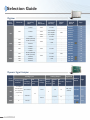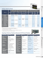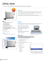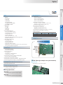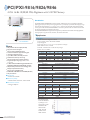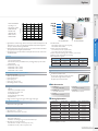
1
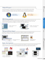
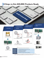
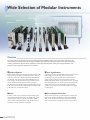
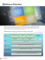
Software Overview
ADLINK delivers robust software support for their comprehensive line of DAQ cards in a variety of form factors: USB, PCI Express®, PCI,
CompactPCI, and PXI. ADLINK offers driver for mainstream Windows and Linux Operating Systems, and provide various SDK support
for third-party applications including Visual Studio, LabVIEW™ and MATLAB®. In addition, ADLINK also provides componentware for
measurement and HMI, and ready-to-run Application, like Data Logger software.
ADLINK Software Supporting Microsoft® Windows® Frameworks
Visual Studio .NET
LabVIEW™
ActiveX Control
&.NET Assembly
VI for LabVIEW™
MATLAB®
DAQ Toolbox for
MATLAB®
Ready to Run
Applications
DAQBench
DASK Low Level API
D2K-DASK, PCIS-DASK, WD-DASK, UD-DASK, DSA-DASK
Windows XP, and Windows 7/8 x64, x86 edition
ADLINK DAQ Cards in Various Form Factor: PCI, PCI Express, CompactPCI, USB, PXI
(General-purpose DAQs, Digital I/O, Analog Output, Performance DAQ, High-Speed Digital I/O, Digitizers)
* National Instruments and LabVIEW are trademarks of National Instrument, Inc.
* MATLAB® is a trademark of The MathWorks, Inc.
2-1
www.adlinktech.com
Multiple OS Support
1
PXI/PXIe
For different operating systems, we design API with the native programming logic, so users can simply install the driver without modifying
the program when migrating between different operating systems. ADLINK provides drivers to support Windows 2000/XP, Windows 7/8
(x86 and x64) and Mainstream Linux distributions: Ubuntu, Fedora. And also provides legacy driver/SDK for legacy ISA-bus DAQ Cards.
Windows 2000/XP
Linux
Windows 7/8 x64/x86
Ubuntu
Fedora
2
SDK & Componentware
ActiveX Controls/.NET Assembly, Express VI and Polymorphic VI for LabVIEW and DAQ Toolbox for MATLAB. For Low Level API, we also provide
DASK Native Libraries for different product lines. DAQBench is the componentware for developing HMI application.
DAQPilot : ADLINK Task-oriented
DAQBench : 32-Bit ActiveX Controls for
SDK for Windows
Measurement and SCADA/HMI
Modular Instruments
ADLINK provide various SDK to its comprehensive line of data acquisition products. DAQPilot is a task-oriented Software Development Kit, include
3
DAQ
Third-party Software Support
For LabVIEW users, ADLINK provide Express VI and Polymorphic VI libraries. For MATLAB users, ADLINK provides MATLAB Data Acquisition
Toolbox Adapter for all DAQ Cards. In addition, ADLINK is a Math Works Connections Program partner for long term product support.
Express VI and Polymorphic VIs
MATLAB® DAQ Toolbox for
for LabVIEW™
ADLINK DAQ Cards
4
ADLINK provides various ready-to-run applications, like AD-Logger, a Data logger Software; DAQMaster, a configuration tool for data acquisition devices
requiring no programming, and specific ready-to-use utilities for USB DAQ by U-Test and for Dynamic Signal Acquisition Modules by DSA-Utility.
AD-Logger : Configuration-Based
DAQMaster : Configuration-Based
U-Test : Full function testing
Data Logger for ADLINK DAQ Cards
Device Manager for ADLINK DAQ Cards
of ADLINK USB DAQ
www.adlinktech.com 2-2
GPIB & Bus Expansion
Ready to Run Application
8 Steps to Get ADLINK Products Ready
Install the DAQ Card /
Install System Manager
Install the Driver for
Module
Configure and Test
Windows
Open the Box
ADLINK DAQ Cards / Modules
Install
ADLINK Product Package
Insert the ADLINK All-in-one CD
Insert the ADLINK All-in-one CD
PXI Platform
Click ”Driver Installation”
ADLINK DAQ Cards / Modules
ADLINK All-in-one CD
Click ”DAQMaster*” for installation
to install ADLINK DASK Drivers
PCIS-DASK
ADLINK PCI/PCIe/cPCI Series DAQ Cards
D2K-DASK
ADLINK DAQ/DAQe/PXI-2000 Series Cards
WD-DASK
ADLINK High-Speed Digitizers
UD-DASK
ADLINK USB DAQ Modules
DSA-DASK
ADLINK Dynamic Signal Acquisition Modules
Fanless Embedded Computer
Industrial Computer
NOTES: *Please download Windows drivers and API Library from the corresponding product page at the ADLINK website.
*Linux drivers and API Library are also available. For more information, please visit http://www.adlinktech.com/MAPS/linux_daq.html
*DAQMaster support for ADLINK DAQ/DAQe/PXI-2000, 6000, 8000, 91XX, 92XX Series Cards.
2-3
www.adlinktech.com
1
PXI/PXIe
ADLINK provides the key concepts of data acquisition and aims to help you get started quickly. The diagram takes you
through the eight steps of driver installing, system manager configuring and testing, SDK & ready-to-run applications
installing of your data acquisition application. Using these eight steps will reduce your hardware set-up and software
development time for your data acquisition applications!
2
Modular Instruments
Ready for
Install Ready-to-run
Install SDK
Development
Application
Reboot System
3
DAQ
For Visual Studio .NET
DASK API & DAQPilot
For MATLAB
For DSA Module
DSA-Utility
4
DAQ-MTLB
For USB DAQ
U-Test
For LabVIEW
GPIB & Bus Expansion
Reboot the System
DAQPilot
For DAQ
AD-Logger
DAQPilot
Task-oriented SDK for ADLINK DAQ Cards
DAQ-MTLB
MATLAB ® Data Acquisition Toolbox Adapter for ADLINK DAQ Cards
DSA-Utility
Utility for ADLINK Dynamic Signal Acquisition Modules
U-Test
Utility for USB DAQ Modules
AD-Logger
Configuration-based Data Logger
NOTE: Please download the SDK and ready-to-run applications from the corresponding product page at the ADLINK website.
www.adlinktech.com 2-4
Wide Selection of Modular Instruments
Overview
From entry-level to high-end, data acquisition to digital input/output, ADLINK provides a diversity of modular instruments with
market-leading price/performance ratio, for bigger and better measurement and automation systems. Now high-speed digitizer,
switching, simultaneous data acquisition, high-density multi-function data acquisition, analog output, digital multimeter, and
arbitrary waveform generator categories are all available.
High-Speed Digitizers
Dynamic Signal Analyzer
Digitizers offer quick and precise input signal acquisition and are widely
A dynamic signal analyzer provides highly accurate measurements and
used in IC testing, video testing, automatic test equipment, radar and
analysis widely used in audio testing, acoustic measurements,
sonar testing, among others. Digitizers optimized for automated test
environmental noise testing, vibration analysis, NVH measurement,
take advantage of the high-throughput PXI and PXI Express buses to
machine condition monitoring, and rotating machinery evaluation.
lower test times, and offer picosecond-level synchronization between
ADLINK’s PCI/PXI-9527 features a high resolution of 24 bits, two analog
modules. ADLINK provides full spectrum modules including the
inputs with sampling rates up to 432 kS/s and two analog outputs with
PXIe-9848 8-CH 14-bit 100 MS/s digitizer, the PCI/PXI-98X6 Series with
update rates up to 216 kS/s. The PCI/PXI-9527 offers the flexibility
4-CH 16-bit and 10/20/40 MS/s, the PCIe-9852 with 200 MS/s 14-bit
needed to create a wide variety of automatic test systems with optimal
2-CH performance, and many other choices.
cost-performance.
Switches
Arbitrary Waveform Generators
Switches are widely used in automatic test equipment (ATE), process
Arbitrary waveforms generate user-defined signals in automation and
control systems, data acquisition systems, etc. ADLINK offers several
measurement application. The TE-5201, a single channel PXI-based
types of switches to meet your application requirements. ADLINK
AWG, provides a high-speed waveform to stimulate signal distortion,
switches include 16-CH general-purpose relays, 24-CH scanners or
power line cycle dropouts, video signals, and power supply transience.
multiplexers, and a 32 cross-point two-wire matrix.
2-5
www.adlinktech.com
1
Digitizer Applications
PXI/PXIe
For quantifying and analyzing physical energy
Leveraging processing power and high-resolution display of PC – PC-based oscilloscope
Defining custom measurement functions by software, such as spectrum analysis,
frequency domain analysis, rise/fall time of signals, and more
PCIe/PXIe-9852
Sampling Rate
200 MS/s 14-Bit 2-CH
High Speed Digitizers
Distributed Temperature Sensing
P 2-11
PCIe/PXIe-9842
Video Signal
200 MS/s 14-Bit 1-CH
High Speed Digitizers
P 2-15
100 MS/s 14-Bit 8-CH
High Density Digitizers
P 2-9
PXI-98x6
Power Supply Unit Testing
10/20/40 MS/s 16-Bit
4-CH Digitizers
Radar & LiDAR
P 2-13
Modular Instruments
PXIe-9848
2
Military & Education
PCI/PXI-9820
P 2-16
65 MS/s 14-Bit 2-CH
PCI/PXI Digitizers
20 MS/s 10/12-Bit 4-CH
PCI Digitizers
Power & Energy
P 2-17
3
DAQ
PCI-9812/9810
PXIe-9529
Sound & Vibration
24-Bit 192 kS/s 8-CH
High-Resolution DSA
P 2-18
PCI/PXI-9527
24-Bit 432 kS/s
High-Resolution DSA
12-Bit
14-Bit
16-Bit
24-Bit
P 2-19
4
Resolution
GPIB & Bus Expansion
Digitizers v.s. DAQs
How to make the choice between a Data Acquisition (DAQ)
board and a High-Speed Digitizer?
Sampling Rate
The difference between a digitizer and standard DAQ is the sampling rate and the
bandwidth. A digitizer can extend its sampling rate from MS/s to GS/s grade, and the
bandwidth can also extend from 10 MHz to GHz. Additionally, the input impedance or the
module’s memory capacity can provide more options for use in different application
environments. Given the features of what are referred to as high accuracy signals, only a
digitizer with high sampling rate and high bandwidth can successfully accomplish the task.
Sampling rate from MS/s to GS/s
Bandwidth ranges from 10 MHz to GHz
Input impedance : 50 Ω, 75 Ω,…high impedance
Onboard memory support (512 MB, 1 GB, …)
Resolution
8-Bit
14-Bit
24-Bit
www.adlinktech.com 2-6
Selection Guide
Digitizer
Form
Factor
Channels
Sampling
Rate
40 MS/s
4-CH
20 MS/s
10 MS/s
PCIe
2-CH
1-CH
Onboard
Memory
16-Bit
512 MB
12-Bit
PCI
2-CH
Input
Resolution
32 k samples
PXI
PXIe
2-13
PCI-9812A
2-17
PCI-9812
2-17
32 k samples
PCI-9810
2-17
512 MB
-
PCI-9816
2-13
512 MB
-
PCI-9820
2-16
1 GB
-
PCIe-9852
2-11
-
-
PCIe-9842
2-15
-
PXI-9846
2-13
-
PXI-9826
2-13
-
PXI-9816
2-13
512 MB
2-CH
PXI-9820
2-16
512 MB
-
PXIe-9848
2-9
14-Bit
512 MB
16-Bit
65 MS/s (External)
60 MS/s (Internal)
2-13
PCI-9826
16-Bit
10 MS/s
2-CH
PCI-9846
10-Bit
200 MS/s
20 MS/s
Page
3-CH
40 MS/s
4-CH
Module
Name
-
128 k samples
65 MS/s (External)
60 MS/s (Internal)
Digital
Input
14-Bit
8-CH
100 MS/s
2-CH
200 MS/s
1 GB
-
PXIe-9852
2-11
1-CH
200 MS/s
-
-
PXIe-9842
2-15
Dynamic Signal Analyzer
Analog Input
Form
Factor
Analog Input
Channels
Max.
Sampling
Rates (S/s)
Analog Output
AD
Resolution
(bits)
FIFO Size
(sample)
Voltage
Output
Channels
Digital IO
Update
Rate
(S/s)
DA
Resolution
(bits)
5K
16
216 kS/s
24
-
-
-
-
Digital IO
Module
Name
Page
PCI-9524
2-21
PCI-9527
2-19
PXI-9527
2-19
4+4 (4-ch
load cell inputs
PCI
PXI
PXIe
2-7
www.adlinktech.com
& 4-ch general
Up to 30 kS/s
2
purpose AD)
2
256 K
8 DI, 8 DO
(Isolated)
24
432 kS/s
4096 k
8
192 kS/s
-
PXIe-9529
2-18
1
OS Information
Products
Page
Software Compatibillity
Windows®
Linux®
LabVIEW™
(Note1)
(Note2)
(Note3)
Visual
Studio.NET
MATLAB®
(Note5)
(Note4)
Software Recommendations
DAQBench
DAQ
Master
AD
Logger
v
v
v
High Resolution
2-17
PCI-9812
2-17
v
v
v
PCI/PXI-9820
2-16
v
v
v
PCI/PXI-9816
2-13
v
v
v
PCI/PXI-9826
2-13
v
v
v
PCI/PXI-9846
2-13
v
v
v
PCIe/PXIe-9842
2-15
v
PXIe-9848
2-9
v
PCIe/PXIe-9852
2-11
v
PCI-9524
2-21
PCI/PXI-9527
2-19
PXIe-9529
2-18
PCIS-DASK
PCIS-DASK/X
DAQPilot
WD-DASK
PCIS-DASK
WD-DASK/X
WD-DASK
DAQPilot
DAQ-MTLB
PCIS-DASK/X
DAQPilot
DSA-DASK
WD-DASK
DAQPilot
DAQ-MTLB
v
v
v
v
Others
2
DSA
Modular Instruments
Digitizers
PCI-9810
PXI/PXIe
Software Selection Guide
Utility
Note.
3
(1) Windows Support for Windows 2000/XP, and Windows 7/8 x64/x86
(2) Linux Support for Ubuntu 12.04.1 LTS, Fedora Core 17, and OpenSuSe 12.1
DAQ
(3) Compatible with LabVIEW™ 8.0 and above
(4) Compatible with Visual Studio .NET 2005/2008, DASK for API, and DAQPilot for Componentware
(5) MATLAB® Data Acquisition Toolbox 2.2 (and above) compliant
High Speed Arbitrary Waveform Generator & PXI Switch Modules
Model Name
TE-5201
Analog Output
1-CH
DAC
Resolution
Update Rate
Output
Impedance
Standard
Waveform
Arbitrary
Waveform Memory
PXI-7901
PXI-7921
PXI-7931
Description
Generalpurpose
Two-wire
Multiplexer
4-groups 2x4
Two-wire Matrix
No. of Channel
16
80 mVpp to 8 Vpp into
Relay Type
SPDT (1 Form C)
DPDT (2 Form C)
DPDT (2 Form C)
50 Ω load
Max. Switching
3 A @ 20 VDC
2 A @ 30 VDC
2 A @ 30 VDC
220 VDC, 250 VAC
220 VDC, 125 VAC
220 VDC, 125 VAC
50 VA, 60 W
50 VA, 60 W
50 VA, 60 W
3A
2A
3A
10 µA @ 10 mVDC
10 µA @ 10 mVDC
10 µA @ 10 mVDC
150 mΩ max.
100 mΩ max.
150 mΩ max.
2-23
2-24
2-24
14-Bit
50 S/s to 100 MS/s
50 Ω
Current
Max. Switching
Sine, Triangle, Square,
Voltage
Pulse, Ramp, Sinc,
Max. Switching
Gaussian Pulse,
Power
Exponential Decay/
Max. Carrying
Rise Pulse,Noise, DC
Current
1 M points
Sample Clock
FM, FSK, Ramped FSK,
Modulation
Sweep
Page Number
2-22
Failure Rate
Contact
Resistance
Page Number
24 (two-wire)
48 (one-wire)
32 (two-wire)
www.adlinktech.com 2-8
4
GPIB & Bus Expansion
Output Range
Model Name
PXIe-9848
8-CH 14-Bit 100 MS/s High-Speed PXI Express Digitizer
Introduction
The ADLINK PXIe-9848 is a 8-CH 14-bit 100 MS/s digitizer for high frequency and wide dynamic range signals
with an input frequency up to 100 MHz. The 100 MHz bandwidth analog input with 50Ω impedance receives
±0.2 V or ±2 V high speed signals. With a PCI Express bus interface and ample onboard acquisition memory up to
512 MB, the PXIe-9848 easily manages simultaneous 8-CH data streaming.
Equipped with high speed and high linearity 14-bit A/D converters, the PXIe-9848 is ideal for applications requiring
high-speed data acquisition, such as power module testing, LIDAR testing, and video signal analysis.
Highlights
Features
■
■
■
■
■
■
■
■
■
■
PXI Express specification Rev. 1.0 compliant
Up to 100 MS/s sampling rate
8 simultaneously analog inputs
High resolution 14-bit ADC
Up to 100 MHz bandwidth for analog input
512 MB onboard storage memory
Programmable input voltage range of ±0.2 V or ±2 V
Scatter-Gather DMA data transfer for high speed data streaming
One external digital trigger input
Full auto-calibration
■OS Information
• Windows XP/7/8, x64/x86
• Linux
■Flexible Use Options
The PXIe-9848 provides a flexible input range from ±0.2V to ±2V, software selectable 50Ω or 1MΩ input impedance, a
wide variety of triggering options, and tight synchronization capability, all maximizing convenience of use.
■High Density Simultaneous 8-CH Data Streaming
Benefiting from PXIe architecture, the PXIe-9848 easily manages simultaneous 8-CH data streaming. Users
can synchronize multiple PXIe-9848 digitizers to mount
a test system providing up to 64 channels in a single
9-slot PXI Express chassis.
■Extra Buffering
The PXIe-9848 provides built-in memory up to 512
MB for massive data storage, enabling users to extend
acquisition for preset durations.
■Software Compatibility
• LabVIEW, MATLAB, Visual Studio, Visual Studio.NET
Equipped with ADLINK PXES-2590 PXIe chassis and PXIe-9848 modules,
high density testing system with up to 64 channels can be implemented.
Note: For PXES-2590 details, please refer to pages 1-13.
Specifications
Analog Input
IO connector definition
TRG IN
CH0
CH1
CH2
CH3
CH4
CH5
CH6
CH7
■
Number of channels: 8 single-ended
■
Input impedance: 50Ω or 1MΩ, software selectable
■
Input Coupling: AC or DC, software selectable
■
Input signal range: ±0.2 V or ±2 V
■
Overvoltage protection: ±5 V
■
ADC resolution: 14 bits, 1 in 16384
■
Crosstalk: < -80 dB from DC to 1 MHz, for all input ranges
■
-3 dB bandwidth: 100MHz
■
Offset error: ±1 mV
■
Gain error: ± 0.5%
■
System noise:
■
Spectral Characteristics
• Sampling rate: 100MS/s
• SINAD: 65 dB
• SNR: 66 dB
• THD: -72 dB
• ENOB: 10.58 bit
• SFDR: 74 dB
2-9
www.adlinktech.com
Typical values are measured using 1 MHz sine wave input at 100 MS/s with amplitude at -1dB of full scale on a ± 2V range. Acquired data lengths are in 64k points, calculated with Hanning window FFT.
Digitizers
1
■ I/O Connector:
• SMB x 8 for analog inputs
• SMB x 1 for external digital input
■ Dimensions (not including connectors):
• 160 (W) x 100 (H) mm (6.24” x 3.9”)
■ Bus Interface:
• PCI Express gen 1 x4
■ Ambient Temperature (Operational):
• 0°C to 55°C (32˚F to 131˚F)
■ Ambient Temperature (Storage):
• -20°C to 80°C (-4˚F to 176˚F)
■ Relative Humidity:
• 10% to 90%, non-condensing
■ Power consumption:
Power Rail
Standby current (mA)
+3.3 V
+12 V
5350
470
2
Full load (mA)
5900
500
Certifications
■ EMC/EMI: CE, FCC Class A
3
Ordering Information
■PXIe-9848
8-CH 14-Bit 100 MS/s High-Speed PXI Express Digitizer
DAQ
Data Storage and Transfer
■ 512 MB onboard memory, shared among the eight analog inputs
(64 MB/per channel)
■ Scatter-Gather DMA data transfer
General Specifications
Modular Instruments
Timebase
■ Sample clock source
• Internal: on-board clock (oscillator)
• External: PXI_CLK10 or PXIe_CLK100
• Timebase frequency: 100 MHz
• Sampling rate: 100 MS/s to 1025.9 S/s
• Internal timebase accuracy: < ±25 ppm
PXI/PXIe
Trigger
■ Trigger Source
• Software
• External digital trigger
• Analog trigger from CH0 ~ CH7
• PXI_STAR
• PXI trigger bus [0..7]
• PXIe_DSTARB
■ Trigger Modes
• Post-trigger
• Pre-trigger
• Middle trigger
• Delay trigger
■ External Digital Trigger Input
• Source: Front panel SMB connector
• Configurable threshold: 0.8 mV to 3.3 V, default 1.67 V
• Maximum input overload: -0.5 V to +5.5 V
• Trigger polarity: rising or falling edge
• Pulse width: 20 ns minimum
■PXIe-9848H
8-CH 14-Bit 100 MS/s High Speed PXI Express Digitizer with x15/x50 attenuator
Onboard Reference
■ +2.5 V onboard reference voltage
■ < 3.0 ppm/°C reference temperature drift
■ 15 minutes recommended warm-up
4
Specifacaions
Attenuation ratio
Bandwidth (-3 dB)
DC gain error
Offset error
Passband flatness
Input impedance
Input Capacitance
Compensation Range
SNR
■The
15:1
45 MHz
1%
< ±2mV
< ±0.4 dB
1MΩ
13.75pF
6.5 ~ 30pF
65 dB
50:1
35 MHz
1%
< ±2mV
< ±0.4 dB
920kΩ
15pF
6.5 ~ 30pF
66 dB
attenuator is connected with the PXIe-9848 for all test conditions
■Dimensions:
■Ambient
■Relative
99.5 (W) x 94 (H) mm (3.88” x 3.67”)
Temperature (Operational): 0°C to 55°C (32˚F to 131˚F)
Humidity: 10% to 90%, non-condensing
www.adlinktech.com 2-10
GPIB & Bus Expansion
■Attenuator dedicated fit for PXIe-9848
The attenuator is specifically designed to support the ADLINK PXIe-9848 as a signal conditioning
module, providing 8 simultaneous analog inputs and 15:1 or 50:1 attenuation ratio. Input impedance, analog input connectors, over- voltage protection, and mechanical design make the attenuator board a transparent match with the PXIe-9848. The attenuator delivers the best solution to
measurement range expansion in the PXI system.
PCIe/PXIe-9852
2-CH 14-Bit 200 MS/s High-Speed PCI Express/PXI Express Digitizers
Introduction
The ADLINK PCIe/PXIe-9852 is a 2-CH 14-bit 200 MS/s digitizer for high frequency and wide dynamic range
signals with an input frequency up to 90 MHz. The 90 MHz bandwidth analog input with 50Ω impedance is
designed to receive ±0.2 V, ±2 V, or ±10 V high speed signals. With a PCI Express bus interface and ample
onboard acquisition memory up to 1 GB, the PCIe/PXIe-9852 easily manages simultaneous 2-CH data streaming.
With high speed and high linearity 14-bit A/D converters and high stable onboard reference, the PCIe/PXIe-9852
provides both high accuracy and high dynamic performance, making it ideal for applications requiring high-speed
data acquisition, such as optical fiber and LIDAR testing, and video signal analysis.
PCIe-9852
PXIe-9852
Highlights
Data Streaming Up to 800MB/s
Features
■
■
■
■
■
■
■
■
■
■
■
PCI Express specification Rev. 2.0 compliant (PCIe-9852)
PXI Express specification Rev. 1.0 compliant (PXIe-9852)
Up to 200 MS/s sampling rate
2 simultaneous analog inputs
High resolution 14-bit ADC
Up to 90 MHz bandwidth for analog input
1 GB onboard storage memory
Programmable input voltage range of ±0.2 V, ±2 V, or ±10 V
Scatter-gather DMA data transfer for high speed data streaming
One external digital trigger input and one external trigger output
One external clock input
Full auto-calibration
Supports signal averaging
Based on PCI Express Gen2 technology, the PCIe/PXIe-9852 can stream data on both channels at its maximum
data rate (200 MS/s), and continuously stream data to the host PC at rates up to 800 MB/s. An 8 x 500 GB driver
RAID system (4TB) extends capture sessions to more than one hour.
Onboard Signal Averaging Technology
Every PCIe/PXIe-9852 provides onboard Signal Averaging, allowing detection of small repetitive signals in noisy
environments with no CPU loading, suitable for applications requiring extraction of small signals from background
noise such as optical fiber testing.
Specifications
Analog Input
■
Number of Channels: 2 single-ended
■
Input Coupling: AC or DC, software selectable
■
AC coupling cutoff frequency: 11 Hz
■
-3 dB Bandwidth: 90MHz
■
Input Impedance: 50Ω or 1MΩ, software selectable
■Software Compatibility
■
Input Signal Range: Range: ±0.2 V, ±2 V, or ±10 V
■
Overvoltage Protection:
■
■
■OS Information
• Windows XP/7/8, x64/x86
• LabVIEW, MATLAB, Visual Studio, Visual Studio.NET
• with 50Ω : ±10V sine wave, 7Vrms
• with 1MΩ : ±10V
■
ADC Resolution: 14 bits, 1 in 16384
■
Gain Error: ±0.65% of input
■
Offset error: ±1 mV
■
Crosstalk: < -80 dB
■
Spectral Characteristics
• Input Range:±0.2 V
• Sampling Rate: 200 MS/s
• SINAD: 61.72 dBc
• SNR: 61.77 dBc
• THD: -81.42 dBc
• ENOB: 9.96 bit
• SFDR: 82.75 dBc
■
Spectral Characteristics
• Input Range:±2 V
• Sampling Rate: 200 MS/s
• SINAD: 62.06 dBc
• SNR: 62.11 dBc
• THD: -80.97 dBc
• ENOB: 10.02 bit
• SFDR: 85.87 dBc
2-11 www.adlinktech.com
Digitizers
1
102
20
1920
102.2
20
2010
Certifications
■ EMC/EMI: CE, FCC Class A
3
IO connector definition
DAQ
CLK IN
TRG IN
TRG OUT
CH0
CH1
4
SSI Bus Cables (for multiple card synchronization)
■ACL-eSSI-2/3/4
SSI bus cable for two, three, and four devices
Onboard Reference
■ +5V and +2.5V onboard reference voltage
■ < 3.0 ppm/°C reference temperature drift
■ 15 minutes recommended warmup
Ordering Information
■PCIe-9852
2-CH 14-Bit 200 MS/s High-Speed PCI Express Digitizer
■PXIe-9852
2-CH 14-Bit 200 MS/s High-Speed PXI Express Digitizer
www.adlinktech.com 2-12
GPIB & Bus Expansion
Data Storage and Transfer
■ 1 GB onboard memory, shared among the two analog inputs
■ Scatter-Gather DMA data transfer
+3.3 V
+12 V
+5 V
2
Modular Instruments
Timebase
■ Timebase options
• Internal: onboard synthesizer
• External: CLK IN (front panel)
■ Sampling clock frequency
• Internal: 200M Hz
• External: 40M Hz ~ 200M Hz (CLK IN)
• Timebase accuracy: <±25 ppm
■ External reference clock source: Front panel, SSI PCIe-9852,
PXI_CLK10 or PXIe_CLK100 PXIe-9852
■ External reference clock: 10M Hz or 100M Hz
■ External reference clock input range: 500mVpp ~ 5Vpp (AC/DC compliant)
■ External sampling clock input range: 1Vpp ~ 5Vpp (AC/DC compliant)
General Specifications
■ I/O Connector
• SMA x 2 for analog inputs
• SMA x 1 for external trigger input
• SMA x 1 for external trigger output
• SMA x 1 for external clock input
■ Dimensions (not including connectors):
• PCIe-9852 : 167.64 (W) x 106.68 (H) mm (6.53” x 4.16”)
• PXIe-9852 : 160 (W) x 100 (H) mm (6.24” x 3.9”)
■ Bus Interface: PCI Express Gen 2 x4
■ Ambient Temperature (Operating):
• PCIe-9852 : 0°C to 50°C (32˚F to 122˚F)
• PXIe-9852 : 0°C to 55°C (32˚F to 131˚F)
■ Ambient Temperature (Storage): -20°C to 80°C (-4˚F to 176˚F)
■ Relative Humidity: 10% to 90%, non-condensing
■ Power consumption:
Power Rail
Standby current (mA)
Full load (mA)
PXI/PXIe
Trigger
■ Trigger Source
• Software
• External digital
• Analog inputs
• SSI (PCIe-9852)
• PXI_STAR (PXIe-9852)
• PXI_trigger bus [0..7] (PXIe-9852)
• PXI_DSTARB (PXIe-9852)
■ Trigger Modes
• Post-trigger
• Pre-trigger
• Middle trigger
• Delay trigger
■ External Digital Trigger Input
• Source: Front panel SMA connector
• Compatibility: 3.3V TTL, 5V tolerance
• Input high threshold: 2.0 V
• Input low threshold: 0.8V
• Maximum input overload: -0.5V ~ +5.5V
• Trigger polarity: Rising or falling edge, software programmable
• Pulse width: 20 ns minimum
■ External Digital Trigger Output
• Compatibility: 5V TTL
• Output high threshold: 2.4V
• Output low threshold: 0.2V
• Trigger polarity: Positive or negative
• Pulse width: 50 ns, 100 ns, 150 ns, 200 ns, 500 ns, 1 μs, 2 μs, 7.5 μs, and 10 μs
• Driving capacity: Capable of driving 50Ω load
PCI/PXI-9816/9826/9846
4-CH 16-Bit 10/20/40 MS/s Digitizers with 512 MB Memory
Introduction
PCI-9816/9826/9846
The ADLINK PCI/PXI-9816/9826/9846 are 10 MS/s, 20 MS/s, 40 MS/s sampling 16-bit 4-CH digitizers designed for
digitizing high frequency and wide dynamic range signals with an input frequency up to 20 MHz. The analog input range
can be programmed via software to ±1 V / ±0.2 V or ±5 V / ±1 V, based on the model. With a deep onboard acquisition
memory up to 512 MB, the PXI/PCI-9816/9826/9846 are not limited by the data transfer rate of the PCI bus to enable
the recording of waveforms for extended periods of time.
The PXI/PCI-9816/9826/9846 are equipped with four high linearity 16-bit A/D converters ideal for demanding applications
with a high dynamic range such as radar, ultrasound, and software-defined radio.
Specifications
PXI-9816/9826/9846
Features
■
PXI specifications Rev.2.2 compliant (PXI-98x6)
Supports 5 V and 3.3 V PCI signals
■ Supports the 32-bit /66 MHz PCI interface
■ 4 channels of simultaneous single-ended analog input
■ 16-bit high resolution A/D converter
■ Up to 10 MS/s, 20 MS/s, and 40 MS/s per channel
■ 512 MB on-board memory for data storage
■ Software selectable 50 Ω or 1 MΩ input impedance
■Programmable input voltage range: ±0.2 V / ±1 V or
±1 V / ±5 V
■5.1 MHz, 9.6 MHz, and 20 MHz analog input bandwidth for the
PCI/PXI-9816, PCI/PXI-9826 and PCI/PXI-9846, respectively
■ Multiple module synchronization via the PXI trigger bus or SSI (System Synchronization Interface)
■ Supports scatter-gather DMA transfer
■ 89 dBc SFDR, 79 dBc SINAD and 12.9-bit ENOB (PXI-9816)
■ Fully auto-calibration
■
Analog Input
■ Number of channels: 4 single-ended channels
■ Input impedance: 50 Ω or 1 MΩ, software selectable
■ Input coupling: DC
■ Input range: (±0.2 V, ±1 V ) or (±1 V, ±5 V), depends on model type
■ ADC resolution: 16 bits, 1 in 65536
■ Crosstalk: <-80 dB from DC to 1 MHz, for all input ranges
■ System noise, unit in LSBRMS:
■
■
• Windows XP/7/8, x64/x86
• LabVIEW, MATLAB, Visual Studio, Visual Studio.NET
■Software Recommendations
PXI-9826D
6.0
4.0
PXI-9846D
8.0
5.0
PXI-9846W
15.0
7.0
Input Range
±1 V
±5 V
PCI-9816H
5.0
3.0
PCI-9826H
6.0
4.0
PCI-9846H
8.0
5.0
PXI-9846H
8.0
5.0
Offset error:
■
• AD-Logger, DAQBench
PXI-9816D
PXI-9826D
PXI-9846D/PCI-9846D
@ 50 Ω and 1 MΩ input impedance
±0.2 V, ±1 V
5.1 MHz
Input Range
PCI-9816H
±1 V, ±5 V
5.1 MHz
±1 V, ±5 V
Spectral Characteristics
• Model: PXI-9816D/512
• Input Range: ±0.2 V
• Sampling Rate: 10 MS/s
• SINAD: 76.56 dBc
• SNR: 76.59 dBc
• THD: -95.91 dBc
• ENOB: 12.42 bit
• SFDR: 99.73 dBc
2-13 www.adlinktech.com
PXI-9816D/9826D/9846D/9846W, PCI-9846D
±0.1%
±0.05%
PXI-9846H, PCI-9816H/9826H/9846H
±0.1%
±0.06%
-3dB Bandwidth, typical:
Input Range
■
PXI-9816D/9826D/9846D/9846W, PCI-9846D
±0.2 mV
PXI-9846H, PCI-9816H/9826H/9846H
±0.3 mV
Gain error:
Input Range
±0.2 V
±1 V
Input Range
±1 V
±5 V
■Software Compatibility
PXI-9816D
5.0
3.0
Model Name
Offset error
Model Name
Offset error
■OS Information
Input Range
±0.2 V
±1 V
PXI-9846DW
80 MHz (±1 V)
55 MHz (±0.2 V)
PCI-9826H
PXI-9846H/PCI-9846H
--@ 50 Ω input impedance
9.6 MHz
20 MHz
--@ 1 MΩ input impedance
90 KHz
--9.6 MHz
20 MHz
PCI-9846D
8.0
5.0
Digitizers
1
-20
• Sampling Rate: 10 MS/s
• THD: -88.61 dBc
• ENOB: 12.96 bit
• SFDR: 89.08 dBc
-40
Magnitude (dB)
• SNR: 80.19 dBc
-60
CH2
CH3
-80
-100
-120
0
1
2
3
4
Frequency (Hz)
5
6
x 10
■
Typical values are measured using 1 MHz sine wave input at 10 MS/s with amplitude at -1dB
at full scale on a ±1 V and ±0.2 V range using the PXI-9816. Acquired data lengths are in
64 K point, calculated with Hanning window FFT.
Note that these dynamic parameters may vary from one module to another, with different
■
input signal frequencies and signal amplitudes selected.
■ For detailed dynamic test results of other modules, please refer to the user manual or visit the ADLINK website.
Timebase
Dedicated External Clock Input From Panel
■
Connector type: SMB
Clock type: sine wave or square wave
■ Input impedance: 50 Ω
■ Input coupling: AC
■ Input range: 1 Vp-p to 2 Vp-p
■ Overvoltage protection: 2.5 Vp-p
■
Triggering
Data Storage and Transfer
■
On-board memory: 512 MB, shared among the four AI channels
■ Data transfer: scatter-gather DMA
On-board Reference
■
On-board reference voltage: +5 V
Temperature drift: < 3 ppm/°C
■ Recommended warm-up time: 15 minutes
■
General Specifications
■ I/O Connector
• BNC X4 for analog inputs
• SMB X2 for external digital trigger and external timebase input
■ Dimensions (not including connectors)
• PCI-98x6: 167.6 mm (W) x 107 mm (H) (6.53" x 4.17")
• PXI-98x6: 160 mm (W) x 100 mm (H) (6.24" x 3.9")
PCI Bus Interface
• PCI signaling: support 3.3 V and 5 V signaling
• PCI interface: 32-bit, 66 MHz
■ Ambient temperature (Operational):
• 0°C to 55°C (32˚F to 131˚F) (PXI version)
• 0˚C to 50˚C (32˚F to 122˚F) (PCI version)
■ Ambient temperature (Storage): -20˚C to 80˚C (-4˚F to 176˚F)
■ Relative humidity: 10% to 90% non-condensing
■ Power Requirement, typical:
Power Rails
3.3 V
5V
12 V
PXI/PCI-9816
0.8 A
1.4 A
0.3 A
PXI/PCI-9826
0.8 A
1.5 A
0.3 A
2
PXI/PCI-9846
0.8 A
2.0 A
0.3 A
Certifications
■ EMC/EMI: CE, FCC Class A
3
Multi-Module Synchronization
■ For PXI version of digitizer modules, they can be synchronized through PXI trigger bus, PXI Star and PXI 10 MHz.
■ For PCI version of digitizer modules, they can be
synchronized through a dedicate interface,
SSI (System Synchronized Interface).
SSI bus cable for multiple
module synchronization
Cable Accessories
■
■
SMB-SMB-1M
1 meter SMB to SMB cable
■ACL-SSI-3
SMB-BNC-1M
1 meter SMB to BNC cable
■ ACL-SSI-2
SSI Bus cable for 2 devices
■ACL-SSI-4
SSI Bus cable for 3 devices
SSI Bus cable for 4 devices
Ordering Information
Model Name
PCI-9816H/512
PCI-9826H/512
PCI-9846H/512
PCI-9846D/512
PXI-9816D/512
PXI-9816H/512
PXI-9826D/512
PXI-9846D/512
PXI-9846DW/512
PXI-9846H/512
Sampling Rate
10 MS/s
20 MS/s
40 MS/s
40 MS/s
10 MS/s
10 MS/s
20 MS/s
40 MS/s
40 MS/s
40 MS/s
Input Range
±5 V, ±1 V
±5 V, ±1 V
±5 V, ±1 V
±1 V, ±0.2 V
±-1 V, ±0.2 V
±5 V, ±1 V
±1 V, ±0.2 V
±1 V, ±0.2 V
±1 V, ±0.2 V
±5 V, ±1 V
Max. -3dB Bandwidth
5.1 MHz
9.6 MHz
20 MHz
20 MHz
5.1 MHz
5.1 MHz
9.6 MHz
20 MHz
80 MHz
20 MHz
Note: For special features or specifications, such as higher input range or higher bandwidth options,
please contact ADLINK for more details.
www.adlinktech.com 2-14
4
GPIB & Bus Expansion
■
Trigger sources:
• software
• TRG IO (front panel SMB connector)
• Analog trigger from CH0 - CH3
• PXI Star (PXI version)
• PXI Trigger Bus[0..7] (PXI version)
• SSI (PCI version)
■ Trigger modes: Pre-trigger, post-trigger, middle-trigger, delay-trigger
PCI-9816/9826/9846
DAQ
■ Sample clock sources
· Internal: on-board oscillator
· External: CLK IN (front panel SMB connector), PXI Trigger Bus[0..7], PXI 10 MHz,
PXI Star, SSI Bus
■ Timebase frequency range
· PCI/PXI-9816: 1 MHz - 10 MHz
· PCI/PXI-9826: 1 MHz - 20 MHz
· PCI/PXI-9846: 1 MHz - 40 MHz
PXI-9816/9826/9846
■
Modular Instruments
PXI/PXIe
• Input Range: ±1 V
• SINAD: 79.80 dBc
CLK IN
TRG IO
CH0
CH1
0
• Model: PXI-9816D/512
Digitizers
PCIe/PXIe-9842
1-CH 14-Bit 200 MS/s High-Speed PCI Express /PXI Express Digitizers
Introduction
The ADLINK PCIe/PXIe-9842 is a 1-CH 14-bit 200 MS/s digitizer designed for applications such as LIDAR testing,
optical fiber testing, and radar signal acquisition. The 100 MHz bandwidth analog input with 50 ohm impedance is
designed to receive ±1 V high speed signal. With this simplified front-end design and high stable onboard reference,
the PCIe/PXIe-9842 not only provides high accuracy measurement results but also delivers high dynamic performance.
PCIe-9842
For applications that require data to be acquired and transferred in real time, the PCIe/PXIe-9842 utilizes the PCI
Express x4 bus as its interface. When signals are converted from analog to digital data, data transfer to host system
memory is continuous, enabled by the PCI Express’ increased bandwidth.
PXIe-9842
Features
■
PXI Express specification Rev. 1.0 compliant (PXIe-9842)
■ Up to 200 MS/s sampling rate
■ High resolution 14-bit ADC
■ ±1 V Input range with 50 Ω input impedance and DC couple
■ Up to 100 MHz bandwidth for analog input
■ High speed PCI Express Gen 1 x4 bus interface
■ Scatter-Gather DMA data transfer for high speed
data streaming
■ One external digital trigger input
■ One digital trigger output to stimulate external
instruments
■ Full auto-calibration
■OS Information
• Windows XP/7/8, x64/x86
■Software Compatibility
• LabVIEW, MATLAB, Visual Studio, Visual Studio.NET
Specifications
Analog Input
■
Number of Channels: One single-ended channel
Input Impedance: 50 Ω ± 2%
■ Input Coupling: DC
■ Input Signal Range: ±1.0 V
■ Overvoltage Protection: ±5 V
■ ADC Resolution: 14 bits, 1 in 16384
■ Offset Error: ±1 mV
■ Gain Error: ±0.5% of input
■ -3dB Bandwidth: 100 MHz
■
Timebase
■ Sample Clock Source: onboard oscillator
■ Timebase Frequency: 200 MHz
Auto Calibration
■ Reference Voltage: +5.000 V
■ Reference Temperature drift: < 5.0 ppm/℃
■ Recommended warm-up time: 15 minutes
2-15 www.adlinktech.com
Trigger
■ Trigger Source
• Software
• External digital
• PXI STAR (PXIe version)
• PXI trigger bus [0..7] (PXIe version)
■ Trigger Mode
• Post-Trigger
■ External Digital Trigger Input
• Compatibility: 3.3 V TTL
• Trigger condition: Rising edge or falling edge, software programmable
• Minimum pulse width: 20 ns
■ Digital Trigger Output
• Compatibility: 3.3 V TTL
• Trigger Condition: Positive or negative, software programmable
General Specifications
■ Ambient temperature (Operational): 0°C to 55°C (32˚F to 122˚F)
■ Ambient temperature (Storage): -20˚C to 80˚C (-4˚F to 176˚F)
■ Relative humidity: 10% to 90% non-condensing
■ Physical
• Dimensions (not including connectors)
- PCIe-9842: 175 mm (W) x 107 mm (H) (6.82" x 4.17")
- PXIe-9842: 160 mm (W) x 100 mm (H) (6.24" x 3.9")
■ IO Connector
• SMA x 1 for analog input
• SMA x 2 for external trigger input and trigger output
■ Bus Interface
• PCI Express Gen 1 x4
Certifications
■ EMC/EMI: CE, FCC Class A
Ordering Information
■PCIe-9842
1-CH 14-Bit 200 MS/s High-Speed PCI Express Digitizer
■PXIe-9842
1-CH 14-Bit 200 MS/s High-Speed PXI Express Digitizer
Digitizers
PCI/PXI-9820
2-CH 14-Bit 65 MS/s PCI/PXI Digitizers with SDRAM
1
PXI/PXIe
Introduction
ADLINK’s PCI/PXI-9820 is a 65 MS/s, high-resolution PXI digitizer with deep SODIMM SDRAM memory. The device
features flexible input configurations, including programmable input ranges and user-configurable input impedance. With
the deep onboard acquisition memory, the PCI-9820/PXI-9820 is not limited by the 132 MB/s bandwidth of PCI bus and
can record the waveform for a long period of time. The PCI-9820/PXI-9820 is ideal for high-speed waveform capturing,
such as radar and ultrasound applications, as well as software radio applications, or those signal digitizing applications
which need deep memory for data storage.
PCI-9820
Specifications
Features
■
■
■
■
■
■
■
■
■
■
■
■
■
■
14-bit A/D resolution
Up to 60 MS/s (with internal timebase) & 65 MS/s
(with external timebase) sampling rate per channel
Up to 130 MS/s sampling rate in "ping pong" mode
2-CH single-ended bipolar inputs
>30 MHz -3 dB bandwidth
Up to 512 MB onboard SODIMM SDRAM
Programmable ranges of ±1 V and ±5 V
User-configurable input impedance of 50 Ω or
high input impedance
Scatter-gather DMA
Analog and digital triggering
2-CH synchronous digital inputs (PXI-9820)
Fully auto calibration
Multiple modules synchronization capability
■OS Information
• Windows XP/7/8, x64/x86
■
Input Impedance (soldering selectable): 50 Ω, 1.5 MΩ
Crosstalk: < -80 dB, DC to 1 MHz
■ Total harmonic distortion (THD): -75 dB
■ Signal-to-Noise ratio (SNR)
■
Range
SNR
±5V
66 dB
62 dB
±1V
■
■
Spurious-free dynamic range (SFDR): 75 dB
Data transfer: bus-mastering DMA with scatter-gather
Auto Calibration
■ Onboard reference: +5 V
■ Onboard reference temperature drift: 2 ppm/˚C
Stability: 6 ppm/1000 Hrs
• LabVIEW, MATLAB, Visual Studio, Visual Studio.NET
External Timebase Input
• AD-Logger, DAQBench
CLK IN
CLK IN
TRG IO
SDI0
CH0
CH1
Current
Power Rail
5V
PXI-9820
PCI-9820
900 mA typical
895 mA
12 V
305 mA typical
295 mA
3.3 V
500 mA typical (with 512 MB SDRAM)
430 mA (with 512 MB SDRAM)
PCI-9820: direct external timebase input
PXI-9820: 10 MHz input for PLL or direct external timebase input
■ Connector: SMB
■ Impedance: 50 Ω
■ Coupling: AC
■ Input amplitude: 1 Vpp to 2 Vpp
TRG IO
■ Overvoltage protection: 2.5 Vpp
SDI1
■ Frequency range: 500 kHz - 65 MHz
CH0
Certifications
■ EMC/EMI: CE, FCC Class A
Cable Accessories
Cable
Description
PXI-9820
PCI-9820
SMB-SMB-1M
SMB-BNC-1M
ACL-SSI-2
ACL-SSI-3
ACL-SSI-4
1-meter SMB to SMB cable
1-meter SMB to BNC cable
SSI Bus cable for 2 devices
SSI Bus cable for 3 devices
SSI Bus cable for 4 devices
√
√
√
√
-
√
-
√
-
√
Ordering Information
■PCI-9820D
2-CH 14-Bit 65 MS/s Digitizer
Triggering
CH1
3
■ Dimensions (not including connectors)
PCI-9820: 175 mm x 107 mm (6.82” x 4.17”)
PXI-9820: 160 mm x 100 mm (6.24” x 3.9”)
■
■Software Recommendations
± 14 V
±5V
Analog Triggering
■ Modes: pre-trigger, post-trigger, middle-trigger, delay-trigger
■ Sources: CH0 and CH1
■ Coupling: DC
Digital triggering
■ Modes: pre-trigger, post-trigger, middle-trigger, delay-trigger
■ Source: external digital trigger from SMB
■ Compatibility: 5 V/TTL
www.adlinktech.com 2-16
4
GPIB & Bus Expansion
Overvoltage Protection
±1V
■
■Software Compatibility
Range
±5V
General Specifications
■ I/O connector
· BNC x 2 for analog inputs
· SMB x 4 for external digital trigger, external time base,
and synchronous digital inputs
■ Operating temperature: 0˚C to 50˚C (32˚F to 122˚F)
■ Storage temperature: -20˚C to 80˚C (-4˚F to 176˚F)
■ Relative humidity: 10% to 90%, non-condensing
■ Power requirements
2
DAQ
■
Supports a 32-bit 3.3 V or 5 V PCI bus
PXI specifications Rev.2.2 compliant (PXI-9820)
Synchronous Digital Input (For PXI-9820 Only)
■ Number of channels: 2
■ Compatibility: 5 V/TTL
■ Data transer: bus-mastering DMA with scatter/gather
Modular Instruments
PXI-9820
Analog Input
■ Number of channels: 2 simultaneous-sampled single-ended
■ Resolution: 14 bits
■ Maximum sampling rate
· 65 MS/s for 2 inputs
· 130 MS/s for Ping-Pong mode using external timebase
■ Onboard sample memory
· 512 MB
■ Bandwidth (-3 dB): 30 MHz minimum
■ Input signal ranges: (software programmable) ±5 V, ±1 V
■ Input Coupling: DC
■ Overvoltage protection
Digitizers
PCI-9812/9812A/9810
4-CH 10/12-Bit 20 MS/s Simultaneous-Sampling Analog Input Cards
Introduction
ADLINK’s PCI-9812, PCI-9810 and PCI-9812A are 4-CH, 10 or 12-bit, 20 MS/s simultaneous-sampling analog input cards.
The high-speed analog input channels are single-ended, with hardware programmable input ranges of ±1 V, ±5 V and
input impedances of 50 Ω, 1.25 kΩ and 15 MΩ. The onboard 32 k-sample A/D FIFO can buffer so data throughput is
less than 100 Mbytes/s, the FIFO performs as the temporary A/D sample buffer, and as a rule of thumb, no data loss
will occur. When four channels operate at 20 MS/s simultaneously, each sample generates two bytes, resulting in 160
Mbyes/s (4 channels * 20 M * 2 bytes) throughput, which exceeds the peak 132 Mbyte/s bandwidth of PCI bus. To avoid
data loss, the 32 k-sample FIFO is the limitation of sample count. For applications requiring a larger number of samples
at full sampling rate, the PCI-9812A features 128 k sample A/D FIFO for storage.
In addition to the onboard 40 MHz time base, users are able to supply the external time base in either sine wave or
digital forms. The PCI-9810 and PCI-9812 also feature external digital trigger and programmable analog trigger, thus the
conversion start point of multiple cards can be synchronized to external events. The trigger modes include software-trigger,
pre-trigger, post-trigger, middle-trigger and delay trigger, further expands the capabilities of these high-speed devices.
ADLINK’s PCI-9812, PCI-9810 and 9812A deliver cost-effective and reliable data acquisition capabilities and are ideal
for vibration testing, image digitizing, ultrasonic measurement, biomedical research, ATE and other high-end industrial,
scientific, and military applications.
Features
■
Supports a 32-bit 3.3 V or 5 V PCI bus
■ 12-bit A/D resolution (PCI-9812 and PCI-9812A)
■ 10-bit A/D resolution (PCI-9810)
■ Up to 20 MS/s simultaneous-sampling rate
■ >17 MHz -3 dB bandwidth
■ 4-CH single-ended inputs
■ Bipolar analog input ranges
■ User-selectable input impedance of 50 Ω or high-input impedance
■ Onboard 32 k-sample A/D FIFO (PCI-9810 and PCI-9812)
■ Onboard 128 k-sample A/D FIFO (PCI-9812A)
■ Analog and digital triggering
■ External clock input for customized conversion rate
■ Bus-mastering DMA for analog inputs
■ 3-CH TTL digital inputs
■ Compact, half-size PCB
■OS Information
• Windows XP/7/8, x64/x86
■Software Compatibility
• LabVIEW, MATLAB, Visual Studio, Visual Studio.NET
■Software Recommendations
• AD-Logger, DAQBench
Specifications
Analog Input
■ Number of channels: 4 single-ended Resolution
· 12-bit (PCI-9812 and PCI-9812A)
· 10-bit (PCI-9810)
■ Maximum sampling rate: 20 MS/s
■ Input signal ranges, impedance and overvoltage protection
Input RangeModel
±1 V
±5 V
Overvoltage protection
50 Ω
15 MΩ
50 Ω
1.25 kΩ
±2 V
±10 V
■ Accuracy: ±1.5% typical
■ DNL: ±0.4 LSB typical, ±1.0 LSB maximum
■ INL: ±1.9 LSB typical
■ Input coupling: DC
■ Trigger sources: software, analog and digital trigger
(5 V/TTL compatible)
■ Trigger modes: software-trigger, pre-trigger,
post-trigger, middle-trigger & delay trigger
■ FIFO buffer size
· 32 k samples (PCI-9810 & PCI-9812)
· 128 k samples (PCI-9812A)
■ Data transfers: bus-mastering DMA
Triggering
■ Analog Trigger
· Modes: pre-trigger, post-trigger, middle-trigger, delay-trigger
· Source: CH0, CH1, CH2 and CH3
· Slope: rising/falling
· Coupling: DC
· Trigger sensitivity: 256 steps in full-scale voltage range
■ Digital Triggering
· Modes: pre-trigger, post-trigger, middle-trigger, delay-trigger
· Source: external digital trigger
· Slope: rising edge
· Compatibility: 5 V/TTL
· Minimum pulse width: 25 ns
2-17 www.adlinktech.com
Input Impedance
External Sine Wave Clock
■ Input coupling: AC
■ Input impedance: 50 Ω
■ Input frequency: 300 kHz to 40 MHz
■ Input range: 1.0 to 2.0 Vpp
■ Overvoltage protection: 2.5 Vpp
External Digital Clock
■ Input coupling: DC
■ Input impedance: 50 Ω
■ Compatibility: 5 V/TTL
■ Input frequency: 20 kHz to 40 MHz
■ Overvoltage protection: diode clamping, -0.3 V to +5.3 V
Digital Input
■ Number of channels: 3
■ Compatibility: 5 V/TTL with 10 KΩ pull down resistors
■ Overvoltage protection: Diode clamping, -0.3 V to +5.3 V
■ Data transfers: bus-mastering DMA with A/D samples
General Specifications
■ I/O connector
· BNC x 5
· 10-pin ribbon male
■ Operating temperature: 0˚C to 40˚C (32˚F to 104˚F)
■ Storage temperature: -20˚C to 70˚C (-4˚F to 158˚F)
■ Relative humidity: 10% to 90%, non-condensing
■ Power requirements
Device
PCI-9812
PCI-9812A
PCI-9810
+5 V
1.4 A typical
1 A typical
■ Dimensions (not including connectors)
173 mm x 108 mm (6.74” x 4.21”)
Ordering Information
■PCI-9810
4-CH 10-Bit 20 MS/s Simultaneous-Sampling
Analog Input Card with 32 k-Sample A/D FIFO
■PCI-9812
4-CH 12-Bit 20 MS/s Simultaneous-Sampling
Analog Input Card with 32 k-Sample A/D FIFO
■PCI-9812A
4-CH 12-Bit 20 MS/s Simultaneous-Sampling
Analog Input Card with 128 k-Sample A/D FIFO
High-Resolution Modules
PXIe-9529
8-CH 24-Bit High-Resolution Dynamic Signal Acquisition Module
1
The ADLINK PXIe-9529 is a high-performance, high density, 8-CH analog input dynamic signal acquisition module.
The PXIe-9529 features eight 24-bit simultaneously sampling analog input channels. The 24-bit sigma-delta ADC
provides a sampling rate of 192 kS/s at high resolution, making it ideal for higher dynamic range signal measurement. All channels are sampled simultaneously and accept input range up to ±10V, and the analog inputs support
software-selectable AC or DC coupling and 4 mA bias current for integrated electronic piezoelectric (IEPE) sensors.
The module is especially designed to meet the requirements of vibration analysis and audio testing.
Specifications
Number of simultaneously sampled channels: 8
· PXI trigger bus [0..7]
■
Input configuration: Differential or pseudo-differential
■
Input impedance: · Post-trigger
Differential
Pseudodifferential
Configuration
Configuration
Features
Input Impedance
■
Between positive
input and system
ground
1 MΩ
1 MΩ
Between negative
input and system
ground
1 MΩ
50 Ω
• Windows XP/7/8, x64/x86
■
■
■
ADC resolution: 24-bit
■
ADC type: Delta-sigma
Trigger Modes
· Delay trigger
■
External Digital Trigger Input:
· 5 V TTL compatibility
· Trigger polarity: rising or falling edge
· Pulse width: 20 ns minimum
Input coupling: AC or DC, software selectable
AC coupling cutoff frequency: 0.5 Hz
Timebase
■
Onboard oscillator sample clock source
■
80 MHz timebase frequency
Data Storage and Transfer
■
512 MB onboard memory, shared among the eight analog inputs
■ FIFO buffer size: 1,024 samples dedicated for per channel
■ Scatter-Gather DMA data transfer
■ Sampling rate: 192 kS/s maximum,
Onboard Reference
■Software Compatibility
8 kS/s to 54 kS/s in 192 µS/s increments,
54 kS/s to 108 kS/s in 576 µS/s increments,
■
+5.000 V onboard reference voltage
108 kS/s to 192 kS/s in 768 µS/s increments
■
< 5.0 ppm/°C reference temperature drift
■
15 minutes recommended warmup
• LabVIEW, MATLAB, Visual Studio, Visual Studio.NET
■Software Recommendations
• DSA Utility
■
Input signal range: ± 10V, or ± 1V
■
Integrated Electronic Piezoelectric (IEPE):
· Current: 4 mA for each channel
· IEPE compliance: 24 V
■
Overvoltage protection
· Differential : ± 42.4V
■PXIe-9529
8-CH 24-Bit High-Resolution Dynamic Signal Acquisition
Module for PXIe bus
· Pseudo-differential :
■PCIe-9529 (call for availability)
8-CH 24-Bit High-Resolution Dynamic Signal Acquisition Module for PCIe bus
■
Offset error: ± 2 mV max
■
Gain error: ± 0.5% of FSR
■
Crosstalk: < -100 dB
■
THD: < -104 dB
- Positive terminal : ± 42.4V
- Negative terminal : Not protected, rated at ± 2.5V
Trigger
■
Trigger Sources
General Specifications
■
I/O Connector:
· SMB x 8 for analog inputs
· SMB x 1 for external digital input
■
Dimensions (not including connectors)
· 160 (W) x 100 (H) mm (6.24” x 3.9”)
■
Bus Interface:
· PCI Express Gen 1 x4
■
Ambient Temperature (Operational):
· 0°C to 55°C (32˚F to 131˚F)
■
Ambient Temperature (Storage):
· -20°C to 80°C (-4˚F to 176˚F)
■
Relative Humidity:
· 10% to 90%, non-condensing
· Software trigger
· Analog trigger
· External digital trigger
Certifications
■
EMC/EMI: CE, FCC Class A
www.adlinktech.com 2-18
4
GPIB & Bus Expansion
Ordering Information
3
DAQ
■OS Information
■
Modular Instruments
■
PXI Express specification Rev. 1.0 compliant
■ 24-Bit Sigma-Delta ADC
■ 8 simultaneous sampling analog input
■ 192 kS/s maximum sampling rate
■ AC or DC input coupling, software selectable
■ One external digital trigger input
■ Support IEPE output on each analog input, software
configurable
■ Full auto-calibration
2
· PXI STAR trigger
Analog Input
PXI/PXIe
Introduction
PCI/PXI-9527
24-Bit High-Resolution Dynamic Signal Acquisition and Generation Modules
Introduction
The PCI/PXI-9527 is a high-performance, 2-CH analog input and 2-CH analog output dynamic signal acquisition module. This module is specifically designed for audio testing, acoustic measurement, and vibration
analysis applications.
The ADLINK PCI/PXI-9527 features two 24-bit simultaneous sampling analog input channels. The 24-bit
sigma-delta ADC provides a sampling rate up to 432 kS/s at high resolutions, making it ideal for higher
bandwidth dynamic signal measurements. The sampling rate can be adjusted by setting the module DDS clock
source to an appropriate frequency. All channels are sampled simultaneously and accept an input range from
±40 V to ±0.316 V. The PCI/PXI-9527 analog input supports software selectable AC or DC coupling and 4
mA bias current for integrated electronic piezoelectric (IEPE) sensors.
PCI-9527
PXI-9527
Features
■
The ADLINK PCI/PXI-9527 also has two channels of 24-bit resolution, high fidelity analog output. The outputs
occur simultaneously at software programmable rates up to 216 kS/s. A software programmable output range
of ±0.1 V, ±1 V, and ±10 V is available on the output channels.
■Dynamic Signal Assistant
PXI specifications Rev. 2.2 compliant (PXI-9527)
■ 24-bit Sigma-Delta ADC and DAC
ADLINK’s Dynamic Signal Assistant is a ready-to-run software utility designed for dynamic signal acquisition ■
2-CH simultaneous sampling analog input
modules, such as the PCI/PXI-9527. This software ■
2-CH simultaneous updated analog output
provides a windows-based configuration interface ■
432 KS/s maximum sampling rate with software
for setting parameters, in addition to a real-time programmable rate
visualized data display on the screen. An instrument-
■
Programmable input range: ±40 V, ±10 V, ±3.16 V, ±1 V, like user interface is also provided for basic waveform ±0.316 V
generation. The Dynamic Signal Assistant can also log ■
Programmable output range: ±10 V, ±1 V, ±0.1 V
data acquired from hardware modules. With the Dynamic ■
AC or DC input coupling, software selectable
Signal Assistant, signal acquisition and generation can be performed in just a few minutes without any programming ■
Trigger I/O connector for external digital trigger signal
■
Supports IEPE output on each analog input,
software-configurable
Specifications
Analog Input
■
Number of simultaneously sampled channels: 2
■
Input configuration: Differential or pseudo-differential, each channel independently software-selectable
■
Input impedance:
Differential
Pseudodifferential
Configuration
Configuration
Between positive
input and system
ground
1 MΩ
1 MΩ
Between negative
input and system
ground
1 MΩ
50 Ω
Input Impedance
effort.
■
Input coupling: AC or DC, software-selectable on each channel
■OS Information
■
ADC resolution: 24-bit
• Windows XP/7/8, x64/x86
■
ADC type: Delta-sigma
■Software Compatibility
■
Sampling rate: Up to 432 kS/s maximum,
2 kS/s to 432 kS/s in 454.7 µS/s increments
• LabVIEW, MATLAB, Visual Studio, Visual Studio.NET
■Software Recommendations
• AD-Logger, DAQBench, DSA Utility
■
Input signal range: ±0.316 V, ±1.00 V, ±3.16 V, ±10.0 V, ±40.0 V
■
Integrated Electronic Piezoelectric (IEPE)
· Current: 4 mA each channel
independently software-selectable
· IEPE compliance: 24 V
■
Data transfer: DMA
■
FIFO buffer size: 4096 samples shared for AI channels
■
Input Common Mode Range: ±10 V for both differential and pseudo-differential configuration
■
Overvoltage protection
· Differential input: ± 40 Vpk
· Pseudo-differential:
– Positive terminal: ± 40 Vpk
– Negative terminal: ± 10 Vpk
2-19 www.adlinktech.com
High-Resolution Modules
■
AC couple bandwidth
■
Analog output, -3dB bandwidth: 110 KHz
■
AO THD+N
· -0.1dB cutoff frequency: 26 Hz
AI Offset Error
Input
Range
Offset
(±mV)
±40 V
0.5
-101 dB
Recommend Warm-up time: 15 minute
± 10 V
-101 dB
■
Power Requirement
±0.316 V
0.05
· Software trigger
· Analog trigger
Triggers
±40V
±0.5%
· PXI Star trigger (PXI-9527)
±30V~±0.316V
±0.2%
· PXI Trigger bus [0..7] (PXI-9527)
Input Range
· Delay-trigger
■
130 KHz
· Trigger conditions: positive or negative trigger, Number of output channels: 2
■
Output configuration:
■
DAC resolution: 24-bit
■
DAC type: Delta-sigma
■
Update rate:
External digital trigger
· Compatibility: 5 V TTL
independently software-selectable
■
· Trigger polarity: rising or falling edge
· Pulse width: 300 ns minimum
System Timebase Characteristics
1 kS/s to 216 kS/s in 227.3 μS/s increments
FIFO buffer size: 2048 samples for each analog output channel
■
Output signal range: ±0.1 V, ±1 V, ±10 V
■
Voltage output coupling: DC
■
Minimum working load: 600 Ω
■
AO Offset error and gain error:
■
Clock frequency: 80 MHz
■
Accuracy: ±20 ppm, over operating temperature Timebase source
■
Internal (on board): 125 MHz
■
External: PXI backplane 10 MHz (PXI version)
General Specifications
■
I/O connector
· BNC x 4 for analog inputs/outputs
AO Gain Error
±0.1 V
±1 V
±10 V
±0.05 mV
±0.25 mV
±1 mV
0.4%
0.4%
0.4%
Output impedance:
■
Cable
Description
SMB-SMB-1M
SMB-BNC-1M
1 meter SMB to SMB cable
1 meter SMB to BNC cable
Ordering Information
■PCI-9527
2-CH 24-Bit 432 kS/s High-Resolution Dynamic Signal Acquisition and Generation module for PCI bus
■PXI-9527
2-CH 24-Bit 432 kS/s High-Resolution Dynamic Signal Acquisition and Generation module for PXI bus
Pseudodifferential
Configuration
Configuration
50 KΩ
10 KΩ
and 5 V PCI signals
■
Dimensions (not including connectors)
AI0
AI1
AO0
4
AO1
Ext. Trig
PCI-9527
IO connector definition
· PCI-9527: 175 mm (W) x 107 mm (H) (6.82” x 4.17”)
■
Ambient temperature (Operational):
· 0˚C to 55˚C (32˚F to 131˚F) (PXI version)
· 0˚C to 50˚C (32˚F to 122˚F) (PCI version)
■
Ambient temperature (Storage):
· -20˚C to 80˚C (-4˚F to 176˚F)
50 Ω
3
IO connector definition
PCI Bus Signaling: Universal PCI, support 3.3 V · PXI-9527: 160 mm (W) x 100 mm (H) (6.24” x 3.9”)
Differential
10 KΩ
2
Cable Accessories
· SMB x 1 for external trigger
AO Offset
Error
Between
positive and
negative
outputs
Certifications
EMC/EMI: CE, FCC Class A
range
Output Range
50 KΩ
350
■
Ext. Trig
AI0
AI1
AO0
AO1
Relative humidity:
· 10% to 90% non-condensing
PXI-9527
10 KΩ
www.adlinktech.com 2-20
GPIB & Bus Expansion
Between
negative output
and chassis
ground
2330
· Source: front panel SMB connector
Differential or pseudo-differential, each channel 930
310
DAQ
■
software selectable
· Trigger resolution: 24-bit
+5 V
+12 V
· Trigger level: full scale input range
Analog Output
Analog trigger
· Source: AI0, AI1
Bandwidth (-3dB)
±40 V, ±10 V, ±3.16 V, ±1 V,
±0.316 V
Trigger mode:
· Post-trigger
< -100 dB
Full Load (mA)
Modular Instruments
■
Standby
Current
(mA)
Power Rail
Trigger sources:
· External digital trigger
Analog Input Channel Bandwidth
Between
positive output
and chassis
ground
±1V
Measured with ±10 V input
Input signal is 18 Vpp @ 1KHz sine wave
■
Temperature coefficient: ≦ ±5 ppm/°C
■
0.05
Adjacent channel
■
±1 V
Crosstalk
■
-89 dB
0.1
Crosstalk
100 Hz to 20 KHz, 200 kS/s
0.2
AI Gain Error
Onboard reference: +5 V
± 0.1 V
±10 V
Input
Range
■
Output Range
±3.16 V
■
1
Calibration
PXI/PXIe
· -3dB cutoff frequency: 3.5 Hz
High-Resolution Modules
PCI-9524
24-Bit Precision Load Cell Input Card
Introduction
The PCI-9524 is a robust, multi-purpose module designed for turnkey material test systems (MTS). Equipped with four
strain gauge-based full-bridge transducer input channels, four general purpose analog input channels, and a 3-axis motion
controller, the PCI-9524 delivers a complete hardware solution for MTS manufacturers. The PCI-9524 easily integrates
physical quantity measurement and implements strategy of software-based close-loop control in a single module
package. For transducer measurement, the PCI-9524 supports sensitivity from 1.0 mV/V to 4.0 mV/V and provides a
1/200000 accuracy of measurement of full scale. These features make the PCI-9524 suitable for precise measurement in
large-scale transducers.
The PCI-9524 is also equipped with four, 24-bit general purpose analog input channels that allow accurate measurements of the LVDT (Linear Variable Differential Transducer) and Linear wire potentiometer signals to achieve
high-resolution of displacement.
With motion control capability and 16-bit DA channels, the PCI-9524 comes with three stepper/servo motor axes and
two channels of hydraulic system control function. The built-in incremental encoder feedback channels enable the PCI-9524 to
implement the stratagem of MTS’ software-based closed-loop control.
The impressive PCI-9524 features permit easy implementation of required control or measurement functionalities
with just a single module, saving precious development and integration time for MTS manufacturers, CNC machines,
and civil testing equipment.
Features
Transducer Inputs for precise measurement
• 4-CH full-bridge load cell transducer inputs
• Accuracy up to 1/200,000 counts at full-scale
• Sensitivity from 1.0 mV/V to 4.0 mV/V
• 2.5/10 VDC excitation voltage, software selectable
• Internal 24-bit A/D resolution
■ Motion control interface for stepper and hydraulic
system control
• 3-axis PWM output with OUT/DIR and CW/CCW mode
• 2-CH 16-bit analog outputs
• A-B phase encoder input with 24-bit counter
■ General-Purpose Analog Inputs for accurate measure
ments of LVDT1 and linear wire potentiometer signals
• 4-CH analog input with 24-bit resolution
• Programmable gains of ±1.25 V, ±2.5 V, ±5 V, ±10 V
• Up to 30 kS/s sampling rate (single channel)
Specifications
■
Note 1: LVDT: Linear Variable Differential Transducer
■OS Information
• Windows 2000/XP, Windows 7 x64/x86
4-channel Load Cell Transducer Input
■
Excitation voltage: 2.5 V/10 VDC
■
Internal A/D resolution: 24-bit
■
Update speed when Auto-zero Disabled
· Up to 30 KSPS (single channel)
· Up to 1,638 SPS (multi-channel)
■
Update speed when Auto-zero Enabled
Analog Output
■
■
■
■
■
Resolution: 16-bit
Output range: ±10 V
Number of channels: 2
Update rate: Up to 5 kS/s
Onboard 1 K samples D/A FIFO
Driving capability: 5 mA
Hardware Timer Interrupt
· Up to 819 SPS (single channel or multi-channel)
Transducer sensitivity: 1.0 mV/V to 4.0 mV/V
■
■
Base clock: 40 MHz
■
Number of channels: 1.6
■
Resolution: 32-bit
■
Accuracy: 1/200000 of full scale
■
Interrupt Frequency: 40MHz / 2N; N=1~232
(with remote sense & auto zero enabled)
■
Onboard 256 samples A/D FIFO
PWM Output & Encoder Input
■
Number of axis: 3
General Specifications
■
5V power output current:
· ISO5VDD: max. 160 mA
Pulse output options: OUT/DIR and CW/CCW · ISOPWR: max. 16 mA
(26LS31, differential line driver, driving current: up to
■
I/O connector: Two 68-pin SCSI-VHDCI female
20 mA)
■
Operation Temperature: 0 to 45˚C
■
Power requirements: 5 V @ 2 A
■Software Compatibility
■
Maximum output frequency: 500 kHz
■
Encoder Input: 24-bit up/down counter for
■ Dimensions (not including connectors):
156 mm x 116 mm (6.14" x 4.57")
• LabVIEW, MATLAB, Visual Studio, Visual Studio.NET
■Software Recommendations
• DAQBench, DAQMaster
incremental encoder feedback
General Purpose Analog Input
■
Resolution: 24-bit
■
Programmable range: ±1.25 V, ±2.5 V, ±5 V, ±10 V
■
Number of channels: 4
■
Sampling rate: 30 kS/s (non-multiplexing)
■
Onboard 256 samples A/D FIFO
Isolated Digital Input
■
Number of channels: 8
Maximum input range (non-polarity): 0 V to 24 V
■ Input resistance: 2.7 KΩ
■
Isolated Digital Output
2-21 www.adlinktech.com
■
Number of channels: 8
Output type: Power MOSFET
■ Sink current: Up to 300 mA/channel
■
Ordering Information
■PCI-9524
24-Bit Precision Load Cell Input Card
Waveform Generator
TE-5201
125 MS/s Arbitrary Waveform Generator
1
The TE-5201 is a 125 MS/s, full performance, arbitrary waveform generator on a 3U PXI form factor. The
single channel AWG generates waveforms up to 2 MS in length. The clock in/clock out connector provides a
synchronized platform for up to six plug-in arbitrary generators, as well as for other plug-in instruments. Built in
sequencing technology links up to 4096 memory segments and repeats each segment up to 32 k times.
PXI/PXIe
Introduction
Specifications
■
■OS Information
• Windows 2000/XP, Windows 7 x64/x86
■Software Recommendations
• ARBDetector
Ordering Information
Operating Modes
■ Normal: Continuous waveform is generated
■ Triggered: Each input cycle generates a single output cycle
■ Gated: External signal enables generator.
First output cycle synchronous with the active slope of the triggering signal. Last cycle of output waveform always completed
■ External Burst: Preset number of up to 128 k cycles stimulated by an internal, or external.
This mode is not available in Sequencer mode
Trigger Sources
■ External
■ Internal · Range: 100 mHz to 2 MHz
· Input: Front panel BNC
· Level: TTL
· Resolution: 7 digits
· Slope Positive or negative, programmable · Accuracy: 0.1%
· Frequency: 5 MHz to DC
■ Backplane: TTL Trig0 through TTL Trig7, STAR
■ Software: SCPI command
Trigger Input
■ Connector: Front panel BNC
■ Threshold Level: TTL
■ Slope: Positive or negative going edge
■
■
Impedance: 10 k., ±5%
Minimum Pulse Width: 20 ns
General
■
■
Power consumption: 10W max
Current consumption:
· +3.3V: 1.4A max
· +5V: 30mA max
· +12V: 200mA max
· -12V: 200mA max
■ Temperature
· Operating: 0 to 50oC
· Storage: -40 to 70oC
■ Safety: EN61010-1, 2nd revision
www.adlinktech.com 2-22
4
GPIB & Bus Expansion
■TE-5201
125 MS/s Arbitrary Waveform Generator
Sample Clock Modulation
■ FM
· Description: Sample clock can be frequency modulated by internal waveforms that are resident in internal
memory (fixed waveforms)
· Modulation Source: Internal sine square, triangle and ramp
· Modulation Freq. Range: 2 mHz to 100 kHz
- Resolution: 10 digits
- Accuracy: 0.1%
· Peak Freq. Deviation: DC 50 MHz
· Advance: Automatic, triggered, gated or software command
· Marker
- Output and level same as SYNC output.
- Position: Fixed at carrier frequency
3
DAQ
Single channel 125 MS/s PXI-based waveform generator
Sine waves to 50MHz, Square to 30MHz
■ SINE OUT to 125MHz, 1Vp-p
■ 14-bit vertical resolution
■ 2M waveform memory
■ Ultra fast waveform downloads using DMA
■ Low phase noise carrier
■ Internal trigger generation
■ Extensive modulation capabilities AM, FM, Arbitrary FM, FSK, Ramped FSK and Sweep
■ Waveform sequencing with up to 4096 segments and sequences
■
2
Modular Instruments
Features
Waveforms
■ Standard Waveforms
· Waveforms: Sine, Triangle, Square, Pulse, Ramp, Sine(X)/X, Gaussian, Exponential, Repetitive Noise, DC
· Frequency range:
- Sine: 100 μHz to 50 MHz
- Square, Pulse: 100 μHz to 30 MHz
- All others: 100 μHz to 15 MHz
■ Arbitrary Waveforms
· Sample rate: 100 mS/s to 125 MS/s
· Vertical resolution: 14 Bits
· Waveform memory: 2M points standard
· Min. segment size: 16 points
· Resolution: 4 points
· No. of segment: 1 to 4k
· Download rate: 5M points per second
■ Sequenced Arbitrary Waveforms
· Operation: Permits division of the memory bank into smaller segments. Segments may be linked, and
repeated in user-selectable fashion to generate extremely long waveforms
· Sequencer steps: 1 to 4k
· Min. Seg. Duration: 1 μs
· Segment loops: 1 to 1M
Switches
Switch Introduction
To meet the needs of a wide range of uses in the measurement and automation field, switches come in a variety of types and sizes for versatile
applications. It is important to understand the different types of switches available before selecting the most appropriate switch configuration.
General-Purpose (GP) Switches
General purpose switches contain several independent relays which are isolated from each other. GP
switches are commonly used to connect one input to one output and are usually built with Form A
or Form C relays. The normal usage of GP switches is to turn on or turn off devices, such as motors,
fans, heaters, and lights.
Multiplexers (MUX)
In test applications, the quantity of instruments is usually lower due to high cost. Thus, to connect
multiple units under test (UUT) with the testing instrument, a multiplexer is always the choice to
make the maximum utilization of the instruments. A 1-wire multiplexer routes single-ended signals
to one point, and a 2-wire multiplexer selects differential signals. A 4-wire multiplexer is usually used
to measure low resistance or RTDs. The instruments which are often used with multiplexer include
DMM, digitizer and signal source, such as AWG, to provide both measurement and excitation.
Matrix
Matrix switches provide the most versatile switching capacity among these function topologies. In
the matrix, any input can connect to any output individually or in combination. Unlike the multiplexer,
the matrix can connect the source or measurement instrument to multiple UUTs at the same time.
Matrix' advantage is the save of wiring. When users want to change the configurations of measurement or excitation, users just change the internal connection path, and do not have to manually
reconfigure the wiring.
PXI-7901
16-CH General-Purpose SPDT Relay Module
■OS Information
• Windows 2000/XP
■Software Compatibility
• LabVIEW, MATLAB, Visual Studio, Visual Studio.NET
■Software Recommendations
• DAQBench, ADL-SWITCH for Windows
Specifications
Relay Characteristics
Features
■
■
■
■
■
■
■
■
PXI specifications Rev. 2.2 compliant
16-CH SPDT (1 Form C) non-latching relays
Switching capacity: 3 A switching, 3 A carrying / 220 VDC, 250 VAC
125 operations per second for full settling
Onboard 1 k-sample scan list for deterministic scanning
Handshaking signals for external instruments synchronization
Hardware emergency shutdown with programmable relay safety status
8 auxiliary 3.3 V/TTL digital inputs/outputs with 5 V tolerance
2-23 www.adlinktech.com
■ Number of channels: 16
■ Relay type: SPDT (1 Form C), non-latching
■ Switching capacity
· Max. switching current: 3 A
· Max. switching voltage: 220 VDC, 250 VAC
· Max. switching power: 50 VA, 60 W
· Max. carrying current: 3 A
■ Contact resistance: 150 mΩ max.
Auxiliary Digital I/O
■
Numbers of channel: 8 inputs/outputs
■ Compatibility: 3.3 V/TTL (5 V tolerant)
Safety Functions
■ Emergency shutdown
· Logic level: 3.3 V/TTL (5 V tolerant)
· Active: logic low
General Specifications
■ I/O Connector: 62-pin D-sub male
■ Operating temperature: 0˚C to 55˚C (32˚F to 131˚F)
■ Storage temperature: -20˚C to 70˚C (-4˚F to 158˚F)
■ Relative humidity: 5% to 85% non-condensing
■ Power requirements: (when all relays are ON)
■ Dimensions (not including connectors)
· 160 mm x 100 mm (6.24” x 3.9”)
Certifications
■
EMC/EMI: CE, FCC Class A
Ordering Information
■PXI-7901
16-CH General-Purpose SPDT Relay Module
* Failure rate indicates the lower limit of switching capacity of a
relay contact at a reliability level of 60%
Terminal Boards & Cables
■TB-6201-01
General-Purpose Switch Terminal Board with one 62-Pin D-Sub Female Connector for PXI-7901
■ACL-10262
62-pin D-sub male/female cable, 1 M
(For more information about mating cables, please refer to
P3-48.)
Switches
PXI-7921
24-CH 2-Wire Multiplexer Module
1
Safety Functions
• Windows 2000/XP
■Software Compatibility
• LabVIEW, MATLAB, Visual Studio, Visual Studio.NET
■ Emergency shutdown
· Logic level: 3.3 V/TTL (5 V tolerant)
· Active with logic low
■Software Recommendations
• DAQBench, ADL-SWITCH for Windows
Specifications
Source Wire
■
PXI specifications Rev. 2.2 compliant
24-CH DPDT (2 Form C) non-latching relays
■ Switching capacity
• 2 A switching, 2 A carrying
• 220 VDC, 125 VAC
■ Onboard 1 k-sample scan list for deterministic scanning
■ Hardware emergency shutdown with programmable relay safety status
■
One 48x1
2-wire
One 24x1, Two 12x1, Four 6x1
4-wire
One 12x1
General Specifications
■
I/O Connector: 62-pin D-sub male
Operating temperature: 0˚C to 55˚C (32˚F to 131˚F)
■ Storage temperature: -20˚C to 70˚C (-4˚F to 158˚F)
■ Relative humidity: 5% to 85% non-condensing
■
2
Certifications
■
EMC/EMI: CE, FCC Class A
Ordering Information
Relay Characteristics
■PXI-7921
24-CH 2-Wire Multiplexer Module
■ Number of channels: 24 (2-wire)
■ Relay type: DPDT (2 Form C), non-latching
■ Switching capacity
· Max. switching current: 2 A
· Max. switching voltage: 220 VDC, 125 VAC
· Max. switching power: 60 W
· Max. carrying current: 2 A
■ Contact resistance: 100 mΩ max.
* Failure rate indicates the lower limit of switching capacity of a
relay contact at a reliability level of 60%
Terminal Boards & Cables
■TB-6221-01
Multiplexer Switch Terminal Board with One 62-
Pin D-Sub Female Connector for PXI-7921
■ACL-10262
62-pin D-sub male/female cable, 1 M
(For more information about mating cables, please refer to
P3-48.)
4x8 2-Wire Matrix Module
General Specifications
■ I/O Connector: 62-pin D-sub male
■ Operating temperature: 0˚C to 55˚C (32˚F to 131˚F)
■ Storage temperature: -20˚C to 70˚C (-4˚F to 158˚F)
■ Relative humidity: 5% to 85% non-condensing
■ Power requirements: (when all relays are ON)
■ Dimensions
160 mm x 100 mm (not including connectors)
• Windows 2000/XP
■Software Compatibility
• LabVIEW, MATLAB, Visual Studio, Visual Studio.NET
■Software Recommendations
• DAQBench, ADL-SWITCH for Windows
Specifications
Features
■
■
■
■
■
■
■
PXI specifications Rev. 2.2 compliant
Configuration determined by terminal board
Up to 32 cross-point DPDT (2 Form C) non-latching relays
Contact rating
• 2 A switching, 2 A carrying
• 220 VDC, 125 VAC
Onboard 1 k-sample scan list for deterministic scanning
Hardware emergency shutdown with programmable relay safety status
8 auxiliary 3.3 V/TTL digital inputs/outputs with
5 V tolerance
Certifications
Source Wire
Multiplexer
2-wire
One 4x8, Two 4x4, One 2x16, Two 2x8, Four 2x4
Relay Characteristics
■ Number of cross points: 32 (2-wire)
■ Relay type: DPDT (2 Form C), non-latching
■ Switching capacity
· Max. switching current: 2 A
· Max. switching voltage: 220 VDC, 125 VAC
· Max. switching power: 60 W
· Max. carrying current: 2 A
■ Contact resistance: 100 mΩ max.
Auxiliary Digital I/O
■
■
Numbers of channel: 8 inputs/outputs
Compatibility: 3.3 V/TTL (5 V tolerant)
Safety Functions
■
EMC/EMI: CE, FCC Class A
Ordering Information
■PXI-7931
4x8 2-Wire Matrix Module
* Failure rate indicates the lower limit of switching capacity of a
relay contact at a reliability level of 60%
Terminal Boards & Cables
■TB-6231-01
Multiplexer Switch Terminal Board with One
62-Pin D-Sub Female Connector for PXI-7931
■ACL-10262
62-pin D-sub male/female cable, 1 M
(For more information about mating cables, please refer to
P3-48.)
■ Emergency shutdown
· Logic level: 3.3 V/TTL (5 V tolerant)
· Active: logic low
www.adlinktech.com 2-24
4
GPIB & Bus Expansion
■OS Information
3
DAQ
PXI-7931
Modular Instruments
Features
Multiplexer
1-wire
PXI/PXIe
■OS Information