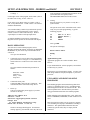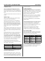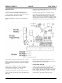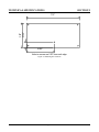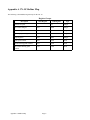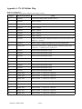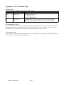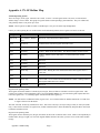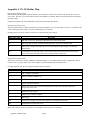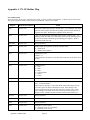
1
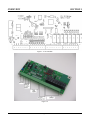
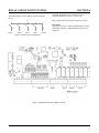
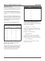
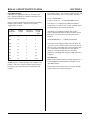
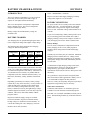
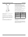
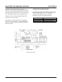
CX-10 USER'S MANUAL Copyright 2009 - Remote Processing Corporation. All rights reserved. However, any part of this document may be reproduced with Remote Processing cited as the source. REV 1 NOTICE TO USER The information contained in this manual is believed to be correct. However, Remote Processing assumes no responsibility for any of the software or circuits described herein, conveys no license under any patent or other right, and make no representations that the circuits are free from patent infringement. Remote Processing makes no representation or warranty that such applications will be suitable for the use specified without further testing or modification. The user must make the final determination as to fitness for a particular use. The contents of this manual and the specifications herein may change without notice. TRADEMARKS Intel is a copyright of Intel Corporation. Windows, Windows XP, and Windows Terminal are trademarks of Microsoft Corporation. Remote Processing Corporation's general policy does not recommend the use of its products in life support applications where the failure or malfunction of a component may directly threaten life or injury. It is a Condition of Sale that the user of Remote Processing products in life support applications assumes all the risk of such use and indemnifies Remote Processing against all damages. Remote Processing is a registered trademark of Remote Processing Corporation. FCC NOTICE The CX-10 was not tested for EMI radiation. When operated outside a suitable enclosure, the board and any cables coming from the board will radiate harmful signals which interfere with consumer and industrial radio frequencies. It is your responsibility to properly shield the CX-10 and cables coming from it to prevent such interference. Remote Processing® Corporation 7975 E. Harvard Ave. Denver, Co 80231 USA Tel: (303) 690 - 1588 Fax: (303) 690 - 1875 email: [email protected] internet: www.rp3.com P/N 2XXX Revision: 1.0 Page i TABLE OF CONTENTS WATCHDOG OVERVIEW SECTION 1 MANUAL ORGANIZATION . . . . . . . . . . . . . . . . MANUAL CONVENTIONS . . . . . . . . . . . . . . . . . BASIC Statement types . . . . . . . . . . . . . . . . . Number convention . . . . . . . . . . . . . . . . . . . . Terminology . . . . . . . . . . . . . . . . . . . . . . . . . . SETUP AND OPERATION SECTION 2 OPERATING PRECAUTIONS . . . . . . . . . . . . . . . INITIAL SETUP . . . . . . . . . . . . . . . . . . . . . . . . . . Serial Port Setup . . . . . . . . . . . . . . . . . . . . . . . MODBUS OPERATION . . . . . . . . . . . . . . . . . . . BASIC OPERATION . . . . . . . . . . . . . . . . . . . . . . . Application Programs . . . . . . . . . . . . . . . . . . . UPLOADING AND DOWNLOADING PROGRAMS . . . . . . . . . . . . . . . . . . . . . . . . . Editing programs and programming hints . . . Downloading Long Programs . . . . . . . . . . . . . Programming Commands . . . . . . . . . . . . . . . WHERE TO GO FROM HERE . . . . . . . . . . . . . . . TROUBLESHOOTING . . . . . . . . . . . . . . . . . . . . . Programming port problems . . . . . . . . . . . . . . 1 1 1 2 2 SECTION 5 RELAY AND OPTO INPUT LINES SECTION 6 ELECTRICAL CHARACTERISTICS . . . . . . . . . 1 Relays . . . . . . . . . . . . . . . . . . . . . . . . . . . . . . . 1 Opto Buffered Inputs . . . . . . . . . . . . . . . . . . . . 1 RELAY OPERATION . . . . . . . . . . . . . . . . . . . . . . 1 Electrical Connection . . . . . . . . . . . . . . . . . . . 1 LED Status . . . . . . . . . . . . . . . . . . . . . . . . . . . 2 Modbus Register Interface . . . . . . . . . . . . . . . 3 Opto Buffered Inputs . . . . . . . . . . . . . . . . . . . . 4 LED Indicators . . . . . . . . . . . . . . . . . . . . . . . . 5 1 1 1 1 2 2 PULSE COUNTERS SECTION 7 APPLICATION PROGRAMS . . . . . . . . . . . . . . . . 6 2 3 3 3 5 5 5 BATTERY CHARGER & POWER SECTION 8 POWER CONNECTION . . . . . . . . . . . . . . . . . . . . 1 Battery Backup . . . . . . . . . . . . . . . . . . . . . . . . 1 POWER CONSUMPTION . . . . . . . . . . . . . . . . . . 1 APPLICATION PROGRAMS . . . . . . . . . . . . . . . . 2 TECHNICAL SPECIFICATIONS SECTION 9 MECHANICAL . . . . . . . . . . . . . . . . . . . . . . . . . . . 1 SAVING DATA TO REGISTERS SECTION 3 Number Types . . . . . . . . . . . . . . . . . . . . . . . . . 1 STORAGE MEDIA . . . . . . . . . . . . . . . . . . . . . . . . 1 DATA REGISTERS . . . . . . . . . . . . . . . . . . . . . . . . 1 COMMANDS . . . . . . . . . . . . . . . . . . . . . . . . . . . . . 1 CX-10 Modbus Map Appendix A Watchdog Timer . . . . . . . . . . . . . . . . . . . . . . . . . . . 4 Non-Volatile Intgeger storage . . . . . . . . . . . . . . . . 4 Volatile Integer storage . . . . . . . . . . . . . . . . . . . . . 4 Volatile Operating System . . . . . . . . . . . . . . . . . . 5 Non-Volatile Setup . . . . . . . . . . . . . . . . . . . . . . . . . 8 High Speed Counters . . . . . . . . . . . . . . . . . . . . . . 10 Non-Volatile Floating Point Storage . . . . . . . . . . 10 SERIAL PORTS SECTION 4 SWITCHED POWER . . . . . . . . . . . . . . . . . . . . . . 1 COM0 SERIAL PORT . . . . . . . . . . . . . . . . . . . . . . 1 Modbus ID’s . . . . . . . . . . . . . . . . . . . . . . . . . . 2 Networking the CX-10 . . . . . . . . . . . . . . . . . . 2 CX-10 interfacing in a system . . . . . . . . . . . . 2 COM3 Baud Rate . . . . . . . . . . . . . . . . . . . . . . 4 RS-485 OPERATING INFORMATION . . . . . . . . 4 RS-485 Termination network . . . . . . . . . . . . . 4 RS-485 transmitter turn-off . . . . . . . . . . . . . . 4 RADIO MODEM . . . . . . . . . . . . . . . . . . . . . . . . . . 5 RF Modem Power ON/OFF control . . . . . . . . 5 ACCESSING SERIAL BUFFERS . . . . . . . . . . . . 5 DISABLING CONTROL-C . . . . . . . . . . . . . . . . . . 5 APPLICATION PROGRAMS . . . . . . . . . . . . . . . . 5 COMMANDS & REGISTERS . . . . . . . . . . . . . . . 6 RS-232 PORT PIN OUT . . . . . . . . . . . . . . . . . . . . 6 Page ii OVERVIEW SECTION 1 DESCRIPTION OVERVIEW SECTION 1 The CX-10 is a intelligent IO controller programmable in BASIC and controlled using modbus. The BASIC is a variation of the original INTEL BASIC-52. that is more suitable to a Modbus IO program. For example, if a specified input were to go low, this could signal a critical condition. The basic could set a flag in a register so that a Modbus IO program could easily recognize a fault condition. Programming is usually done on a PC with a serial port. Additional hardware features include: This manual presents modbus and basic as two separate operating modes within each hardware description. ! Flash EPROM allows program updates in the field MANUAL CONVENTIONS ! ! ! ! ! ! ! without removing any parts. Eight 125VAC relays Eight optically buffered inputs Modbus communication through RF, RS485, or RS232 Temperature compensated 12V battery charger Non volatile EEPROM stores configuration Battery and charge voltage monitor Two pulse counters Part Number 2470 2471 Information appearing on your screen is shown in a different type. Example: *MCS-51(tm) BASIC V2.0 Version: CX-10 Portions Copyright(c)2008 Control Design and (c) 2009 Remote Processing Corp. Build:Feb 02 2009 16:41:10 Description NOTE: Text under this heading is helpful information. It is intended to act as a reminder of some operation or interaction with another device that may not be obvious. IO board with 8 relays, 8 opto buffered inputs, 12V battery charger, One RS-232 programming /display port, One RF, RS232, or RS-485 port programmable for ASCII or modbus. WARNING: Information under this heading warns you of situations which might cause catastrophic or irreversible damage. As above with 900 Mhz spread spectrum modem. Wx[a-b] MANUAL ORGANIZATION Denotes jumper block pins. [a-b] are the pins to connect. <xxx> Paired angle brackets are used to indicate a specific function key on your PC keyboard. For example <esc> means the escape key. Most users initially relate to a device based on what it does physically. Initial concerns are “how do I turn on/off relays” and “how do I get an input”? This manual is organized by input-output functions. Jx-N The CX-10 can be thought of as having two independent operating modes: Modbus and Basic. The board will operate in either mode and both modes can operate simultaneously. For example, modbus can be used to control relays and monitor opto status. A Basic program can do the same. Neither mode is dependent upon the other. However, interactions can occur. For example, a Modbus command may turn a relay on while a Basic command may turn it off. The status of a relay depends upon which mode got to it last. Designates a pin number on a connector. BASIC Statement types There are 4 generic types of BASIC statements: The first type is a command. A command does something, generally an output. Examples of commands are PRINT, CLEAR, and REGWRITE. A function returns a value. Examples are REGREAD, SIN, and GET. The third types are control statements. These include IFTHEN-ELSE, GOTO, GOSUB, and DIM. As such they control or set up the system. Basic can act as a watchdog, actinag as a failsafe if modbus communications should stop. The final type are multi-tasking statements. When multitasking is in effect, the operating system monitors for Basic can also organize IO status and voltages in a way Page 1-1 OVERVIEW SECTION 1 specified events to happen. For the most part, multitasking must be set up in the program. Set up consists of a ON multi-tasking, parameters statement and a subroutine that is executed when conditions are met. Example of multi-tasking is ONTICK. Terminology "A/D" Shorthand for analog-to-digital converter. An A/D "measures" a voltage and converts it into a number from 0 to 4095. Some statements are both functions and commands, depending upon which side of the ‘=’ sign it is on. Some examples include ASC and XBY. "I/O" are input-output devices. On the CX-10, this includes relays and opto buffered inputs. “mSec” shorthand for milli-second, or 1/1000 of a second. Number convention BASIC convention generally uses decimal (numbers between 0 and 9) for data and address information. Numbers may be represented in hexadecimal notation. Any hexadecimal numbers are represented by 0xxH notation. A leading 0 is necessary when the first number begins with any letter between A and F. Up to six digits may be represented in this manner. However, many commands and functions only accept 1, 2, or 4 hex digits. TECHNICAL SUPPORT If you have a question about the RPC-210 and can't find it in this manual, call us and ask for technical support. Technical support hours are 9 AM to 4 PM mountain time. Phone: 303-690-1588 FAX: 303-690-1875 email: [email protected] website: www.rp3.com Page 1-2 OVERVIEW SECTION 1 Figure 1-1 CX-10 Outline Figure 1-2 Page 1-3 SETUP AND OPERATION - MODBUS and BASIC SECTION 2 INTRODUCTION INITIAL SETUP SETUP AND OPERATION SECTION 2 The CX-10 is ready to operate over modbus as soon as you connect it to a PC and apply power. This section describes different modbus hardware connection methods. You will need the following equipment to verify operation for either modbus operation or Basic programming. !CX-10 embedded controller !VTC-9F serial cable !Power supply, 9 to 30 VDC @ 500 ma The CX-10 is programmable in Basic. Generally, Basic operation is independent of modbus. However, interactions can occur. For example, relays can be turned on or off over modbus. A Basic program can perform the same operations. It is anticipated that the Basic program will act as a safety program should communications fail over modbus. Refer to SECTION 4, "SERIAL PORT PIN OUT", for wiring information to make your own serial cable. Connect your external power to the terminals marked “Ext Pwr.” and “Gnd” on the board. External power “+” supply goes to “Ext Pwr.” termial. See Figure 2-1 for location. OPERATING PRECAUTIONS The CX-10 is designed to operate in industrial settings. However it is not indestructible. To avoid damaging the CX-10, observe the following precautions: 1. You may connect a 12V lead acid battery to the terminals marked “Batt” and Gnd”. Battery “+” terminal goes to “Batt” terminal. Limit power supply voltage to 30 volts DC. The board will not operate with AC voltage as a power source. 2. Limit relay connections to 115VAC, 2 amperes. 3. Limit opto buffer inputs to 24 volts. The next steps will take you through communicating to the CX-10 through modbus or a terminal program. Either method can be used to verify initial communication. Figure 2-1 Power and serial connection The next step is communicating to your PC. There are Communication Setup Page 2-1 SETUP AND OPERATION - MODBUS and BASIC two ways to do this: Through the programming port or the modbus port. SECTION 2 CD. It is also available at our website: www.rp3.com/downloads Using the programming port means accessing the Basic operating system. You will be able to download and run Basic programs through this port. You will need a terminal program such as Terraterm, Windows Hyper terminal, or RPTERM to do this. RPTERM is included on the CD or download from www.rpc.com/downloads. If you do not have a modbus program, install PROJECT 3 MM on your PC. You will also need a VTC-9 serial cable. You may, optionally, connect modbus to the RS-485 port. However, your PC must have an RS-485 port on it. RS-485 ports on a PC are rare. Usually you will have to have an RS-232 to RS-485 adapter. Adapters are available from these sources. Using modbus requires modbus network communication software. Project 3 MM, which is included on the CD, may be used for this purpose. In both cases, you will need an RS-232 serial port. If you know your available PC serial port, then go to the next section B-B Electronics JDR microdevices. If you don’t know, or are not sure of an available PC serial port, follow the next set of guidelines. www.bb-elec.com www.jdr.com Generally, RS-485 is used over very long distances and between CX-10 boards. Its implementation will not be discussed in this section. See Section 4 for more info. If you have a serial port built into your PC, this is usually COM1 or COM2. If you are using a USB serial adapter, this can be any number from 4 to 16 (or possibly higher). Connect the VTC-9 serial cable to the modbus port as shown above in Figure 2-1. Note that the key notch on the VTC-9 cable faces to the inside of the board. To figure out what serial ports are available, go to the “Control Panel” on your PC. Since Windows operating systems and configurations vary widely, the following method hopefully will work in your situation. The objective is to get to the Windows Device Manager. If you can get there without the following instructions, so much the better. Connect the DB-9 end to a PC RS-232 serial port (determined from “Communication Setup”) Apply power to the CX-10 (if you have not done so already). Select “Start” for Windows 95, 98, ME, and XP. Windows Vista users click on the Windows logo, usually in the lower left corner of the screen. If you mouse over this icon, a little text box should say “Start”. Find the “Control Panel”. You may need to first select “Settings”. When you first start up Project 3 MM, site ID should default to 11. See Figure 2-2 below. XP users select “System”. Then select the “Hardware” tab, then “Device Manager” Vista users select “Hardware and Sound”, then Device Manager. For all Windows OS, select “Ports (COM and LPT). You should set a list of COM ports available on your PC system. MODBUS OPERATION You will need a modbus program to read and write to the CX-10. The program PROJECT3 MM is included on the Page 2-2 SETUP AND OPERATION - MODBUS and BASIC Figure 2-2 Initial Project 3 Screen Page 2-3 SECTION 2 SETUP AND OPERATION - MODBUS and BASIC SECTION 2 Next step is to set the communication port to match your PC. See “Communication Setup” above to help determine what ports you have available if you do not know. Select the Com port that is connected to the RS-232 modbus port. Click on the “System Setup” tab at the top of the program screen. You should get a screen similar to below. All other parameters under “Serial Port Setup” should not have to be changed. Make sure the Baud Rate is set to 19200. Figure 2-3 Communications Setup Page 2-4 SETUP AND OPERATION - MODBUS and BASIC Now click on the “Site Service” tab at the top left of the program. SECTION 2 Click on the blue “Read(Func03)” button. This initiates a modbus transaction by requesting registers 1-12 from the CX-10. If not already done, set “Start Reg” to 1 and “# of Regs” to 12 as shown below. This will return the status of digital IO and power applied to the board. If all goes well, you should get numbers under the “Data” column (right center of screen). Figure 2-4 Project 3 Modbus Data and Transaction initiation. Note that registers 8 and 9 return external supply voltage to the board and battery charging voltage. If external voltage is 0, then power is connected to the battery terminal. Register 8 returns the supply voltage as a number between 0 and 4095. Register 9 returns the battery backup voltage as a number between 0 and 4095. To convert this reading into volts, multiply the value given by 0.007326. NOTE: Registers 8 and 9 automatically return values in volts only when 12 registers are selected and start register is 1. If you start from a different register or have a different number of registers, you will get a number between 0 and 4095. Relays are read and controlled via registers 10 and 1926. To turn on a few relays, enter the following parameters in this order: Start Reg: 10 Page 2-5 SETUP AND OPERATION - MODBUS and BASIC # of Regs. 1 SECTION 2 to the appropriate communication parameters. If the system still does not respond, refer to TROUBLESHOOTING later in this section. On the right center of the program, under “Data”,click in the white area of “Reg 10" box. Enter a 7. 4. Click on the green “Write (Func 16)” button. If all is OK, 3 relays should click. 3 LED’s on the CX-10 board should be illuminated. Testing. Press the "Enter" key on your PC to verify the '>' symbol returns. The system is now in the “immediate mode” and is ready for you to start programming. Type the following program: You can individually control relays and monitor specific opto inputs. For more information, refer to “Relay control” section to control and read relays. Refer to “Opto Inputs” seconds to read opto input status. 10 20 30 40 A complete Modbus register map is in Appendix A. Registers used for specific IO are listed in each chapter. FOR X = 0 TO 2 PRINT “Hello ”, NEXT PRINT Now type RUN BASIC OPERATION The system will display: You will need a serial terminal program, such as Windows Terminal, Hyperlink, TerraTerm, or RPTERM. RPTERM is on your CD or may be downloaded at our website at: www.rp3.com/downloads 1. Hello Hello Hello Ready > Connect the VTC-9 serial cable to the programming port as shown above in Figure 2-1. Note that the key notch on the VTC-9 cable faces to the inside of the board. Application Programs Application programs are on the CD under “Basic Demos”. If you downloaded CX-10 basic programs, extract them to a directory on your PC. Set your terminal communication parameters as follows: Programs are saved in ASCII file format. You may edit them using Windows Notepad, Wordpad, or your word processor. Baud rate: 19200 Data bits: 8 Parity: None Stop bits: 1 2. 3. UPLOADING AND DOWNLOADING PROGRAMS Connect the serial ports. Connect the DB-9 end to the PC's COM port.. This is determined from “Serial Port Setup” above. Downloading programs means transferring them from your PC (or terminal) to the CX-10. Uploading means transferring them from the CX-10 back to the PC. This section explains how to do both of these procedures using generalized instructions for terminal programs. Power up. Turn on or connect the power supply (if you have not done so already). When uploading or downloading files, select ASCII text format. XMODEM, YMODEM, or other formats are not used. *MCS-51(tm) BASIC V2.0 Version: CX-10 Portions Copyright(c)2008 Control Design and (c) 2009 Remote Processing Corp. Build:Jan 29 2009 10:04:51 Basic does not know when you are typing in a program or if something else (laptop or mainframe) is sending it characters. The upload and download file does not contain any special codes; they are simply ASCII characters. The above message should appear. If a nonsense message appears, your terminal or PC may not be set Page 2-6 SETUP AND OPERATION - MODBUS and BASIC Uploading programs is simply a process of receiving an ASCII file. You or your program simply need to send "LIST" to receive the entire program. SECTION 2 in separate modules, you can download them separately. Modules are assigned blocks of line numbers. Start up code might be from 1 to 999. Interrupt handling (keypad, serial ports) might be from lines 1000 to 1499. Display output might be from 1500 to 2500. The programmer must determine the number of lines required for each section. Downloading a program requires transmitting an ASCII file. As you type in (or download) a line, Basic tokenizes that line. The time to do this depends upon its complexity and how many lines of code have been entered. Basic automatically formats a line for minimum code space. For example, you could download the following line of code: Basic must finish compiling a line before starting the next one. When a line is compiled, a ">" character is sent. This should be your terminal programs pacing character when downloading a program. 10 fora=0to5 When you listed this line, it would appear as: If your communications program (such as HyperTerminal) cannot look for a pacing prompt, set it to delay transmission after each line is sent. A 100 ms delay is usually adequate, but your program may be long and complex and require more time. A result of a short transmission time is missing or incomplete program lines. 10 FOR A=0 TO 5 Spaces are accepted but not stored. The following line: 10 for a = 0 to 5 is compressed and displayed as in the second example above. Spaces are removed. However, spaces as part of a remark or PRINT are not removed. Editing programs and programming hints Files uploaded or downloaded are simply ASCII DOS text files. No special characters or control codes are used. You may create and edit programs using your favorite word processor or editor. Just be sure to save files in DOS text format. Downloading Long Programs The CX-10 has a limited RAM (about 6100 bytes). You can store much larger programs, however (up to 32K). To do this, review the program in the Basic Demo directory under the name “download header.bas” You can copy this code and put it at the start of yours. Essentially this program has the start and end of your program. When you download code, the commands will automatically take care of housekeeping. A technique used to further program documentation and reduce code space is the use of comments in a downloaded file. For example, you could have the following in a file written on your editor: REM Read charge voltage REM and convert to volts You may have trouble downloading long programs, depending upon your terminal. Ideally, your terminal program should recognize a <CR> > sequence before sending the next line. Terminal programs such as Terra term or Hyperterm do not do this. 2200 a = regread(8) *.007326 The first 2 comments downloaded to the RPC-210 are ignored. Similarly, the empty lines between comments are also ignored. Line 2200, with its comment, is a part of the program and could be listed. The major penalty by writing a program this way is increased download time. To reliably download long programs, insert a 100 millisecond delay between each line transmitted. This may or may not be in your terminal program. For Terraterm, click on “Setup” in the top banner, then click on “Serial Port...”. You will get a window prompting you for port, baud rate (set to19200), parity (none), stop bits (1), and flow control (none). At the bottom, set transmit delay to 1 for msec/char and 100 for msec/line. Notice that you can write a program in lower case characters. Basic translates them to upper case. Some programmers put "NEW" as the first line in the file. During debugging, it is common to insert "temporary" lines. Putting in “NEW” ensures that these lines are gone. Downloading time is increased when the old program is still present. If you like to write programs A program named “Download core.bas” in the Basic Page 2-7 SETUP AND OPERATION - MODBUS and BASIC Demo directory is an example of automated download process. This program clears out the old program and prepares for a new one. SECTION 2 If you have multiple programs, things get a bit more complicated. You can have a large number of different programs, all of which can call any of the other programs stored in flash. It might help to these of these programs as stacked on top of each other. The program at the bottom is referred to as ROM 1. The next would be ROM 2, located above the first program. ROM1 can be any length (so long as it can fit into flash). Same is true with ROM 2 and so on (as long as it can fit into flash). Programming Commands The following programming commands are used on the CX-10. For some part they follow the original Basic-52 structure. However, there are some differences due to the nature of the flash in the CPU. For example, baud rates and MTOP are not saved. When editing programs, only the highest numbered ROM can be changed. If you only have one program, then programming is easy. Only NEW, RAM ,FPROG0, PROG, and PROG2 are of concern. Other information concerning program storage structure is not of concern. For the most part, if you have just one program stored to flash, you can treat it as RAM. That is, you can add, delete, or change a line of code. It may take noticeably longer, especially when you have a large program, before you get the ‘>’ prompt. If you have several programs, editing programs gets a bit more complicated. You can have a large number of programs stored in flash EPROM. However, only the largest numbered program can be edited. For example: You have programs in slots 1, 2, and 3. You can only change/edit the program in slot 3 (also called ROM 3). Programs in slots 1 and 2 (ROM 1 and ROM 2) cannot be edited. If you need to change the program in 1 or 2, in this case, you need to do an FPROG0 in RAM to clear out all programs then download them again. >prog 1 8025H Page 2-8 SETUP AND OPERATION - MODBUS and BASIC SECTION 2 WHERE TO GO FROM HERE To retrieve a program, type ROMx, where ‘x’ is the number of the progam. In the above example, that would be 1. Command If you want to do this: Description Turn to Section Know more about serial ports 4 FPROG0 Erases all Basic programs in flash. Use this to start a clean download. Modbus connections, including RF, RS-485, and RS-232 4 PROG Creates a programming slot. You can have as many programming slots as memory can hold. Use memory to save variables and data 3 Relay wiring and ON/OFF control 6 PROG0 Disables program in slot 1 (ROM1) to automatically run on power up or reset. Use opto buffered inputs 6 Use high speed counter 7 PROG2 Enables program in slot 1 (ROM1) to automatically run on power up or reset. Measure charge and battery voltages 8 ROMn Switch to ROM slot numbered ‘n’. If you used PROG above for 3 programs, you can go to ROM 1, ROM 2, or ROM 3 and run it. NEW Refer to the table of contents for a more detailed listing. TROUBLESHOOTING You would probably came to this section because you could not get either the Basic sign on message or talk Modbus to your PC. Refer to the appropriate section below to begin. When in a ROM slot, executing NEW clears out the program in the slot. You can then download or enter a new program. New will return an error if you attempt to clear a program that is numbered lower than the highest. See below. RAM Command to use RAM to run a program. You must be in RAM to use PROG or FPROG0. RROM n You can execute a numbered program (n) in the immediate mode or within a Basic program. When you change programs, basic variables are erased. Variables stored in registers are not affected. You can put this command in your downloaded code to immediately execute a program when download is complete. Programming port problems The following are troubleshooting hints when you can't get anything. 1. Check the power source. There are two board power inputs: Battery and external (solar) power. Generally you should apply power to the external input. This voltage should be above 7 volts. If you are so inclined, measure voltage at U6 and C12, terminal marked “+5V”. Voltage there should be 5 ±0.25 volts. Make sure the 5 volt supply is "clean". If it dips intermittently to 3 volts (due to switching noise or ripple), the card will reset. If the noise is frequent enough, the card will be in permanent reset. Some switching power supplies require a minimum load to operate. Check your power supply specifications. The CX-10 draws about 90 milliamperes when no relays are energized or opto inputs are on. Page 2-9 SETUP AND OPERATION - MODBUS and BASIC The CX-10 CPU will function down to around 3 volts. However any modbus communication may not work and relays may not turn on. Board operation when its internal power is below 4.5 volts. 2. Check the COM0 port (J1). Make sure the VTC-9F serial cable is oriented correctly. The key on the cable corresponds to a silk screen area on the board. Remove the connector from COM0. Refer to the outline drawing earlier in this section. Connect an oscilloscope (preferred) or a voltmeter to pin 3 (Txd) and ground. Pin 3 should be -6 volts or more negative. If you have -6 volts or more,cycle power to the board. If you have a scope attached, you should see a burst of activity. With a volt meter, you should see a change in voltage. Using a Fluke 8060A set to measure AC, you should see a momentary reading above 2 volts. 3. Check the cable. Install the cable and make sure the voltages and output activity are still there. Output is from pin 3 on the VTC-9F. If not, check to make sure something is not shorting the output. Wiring is in SECTION 4, SERIAL PORT PIN OUT. 4. Check the serial parameters on your PC. They should be set to: 19200 baud No parity 8 data bits 1 stop Make sure you have set the communications port on your PC to the one the VTC-9F is plugged into. 5. Receiving a sign on message and can't enter characters. Check U10, pin 8 for at least -6 volts with the serial cable connected to the PC. When it is near 0 volts, the terminal or PC's Txd line is not connected. When you press a character on the terminal or PC, you should see the voltage go positive on the oscilloscope. If all of this fails, call technical support listed in SECTION 1. Page 2-10 SECTION 2 SAVING DATA TO REGISTERS SECTION 3 it can store (0-65535). INTRODUCTION SAVING DATA TO REGISTERS SECTION 3 There are 2 numerical formats data can be saved as: Integer and Floating Point. Additionally, there are two types of media this data can be saved to: EEPROM and SRAM. Data is stored to 4 groups of registers, described below. STORAGE MEDIA Integer and floating point numbers are stored in SRAM and EEPROM. SRAM is temporary, volatile memory in the CPU. When the CPU cycles power or resets, number contents are reset to 0. Registers may be written to SRAM an unlimited number of times. All registers described in this section are accessible over modbus. EEPROM’s retain data after power cycling. EEPROM data is stored in U2 on the CX-10 board. Registers may be written to 1,000,000 times before it wears out. Number Types The CX-10 works with both types of number formats. Each type has features and limitations. Both SRAM and EEPROM may be read an unlimited number of times. Integers are in what is known as a 16 bit format and allows numbers between 0 and 65,535. This format is handy for bit manipulation (such as opto input or relay status). It takes less memory than floating point and is faster to work with. Its primary limitation is the limited number range it can store. It cannot store negative numbers. When should SRAM storage be used? When its contents is expected to change frequently. Frequently, in this case, means once/minute or so. Looked at from a different way, writing to EEPROM once/minute means the part will “wear out” in about 1.5 years. SRAM is useful for holding data used in modbus communications. EEPROM is useful for storing constants, such as time delays, offsets and multipliers. When using Basic (another hidden format), integers and floating point numbers are automatically converted into native format. In Basic, both integers and floats are the same. DATA REGISTERS There are 4 groups of data, or numeric, storage registers shown in the table below. Numeric ranges are inclusive, meaning you can use all the numbers shown. Floating point numbers are stored in a format known as IEEE-754, 32 bit. This is a standard format used by many computers. These numbers take longer to work with and require more memory. This 32 bit data length is a single precision format. It can store floating point numbers in the range of +/- E 127. As a matter of practical use, it can store up to 7 digits of data plus an exponent. Any extra numbers are not to be relied upon. Register range This format has the unfortunate characteristic of returning numbers that are close, but not quite the same as the original. Some examples: Original 80.30001 80.6 80.59999 Numeric type 4001-4256 EEPROM Integers 4501-4628 SRAM Integers 7033-7096 SRAM Floating point 7101-7356 EEPROM Floating point You have 256 integer and floating point numbers that can be stored in EEPROM. You have 128 integers and 64 floating point numbers in volatile SRAM. IEE-754 format 80.3 Media type For all intents and purposes the differences are not significant, less than 0.0001245%. We used terminology such as “faster”, “longer”, more and less memory. These are relative terms. For the most part you can use floating point numbers. Use integers if you run out of floats, keeping in mind the range of values Page 3-1 SAVING DATA TO REGISTERS SECTION 3 COMMANDS The following is a list of Basic commands used to read integer and floating point data. Command Format REGREAD Read data from a register REGWRITE Write data to a register. Page 3-2 SERIAL PORTS BASIC SECTION 4 Under the right conditions, the CX-10 can be networked with other CX-10 or modbus devices. DESCRIPTION SERIAL PORTS SECTION 4 The CX-10 has two serial ports that interface to a variety of devices. In addition, the port designated as COM3 can change “personality” This section describes their characteristics and how to use them. The following paragraph may be important to Basic programmers. Each port has a 256 character interrupt driven circular input and output buffer. This allows characters to be sent out (using PRINT) without slowing down program execution. However, if the PRINT buffer fills, program execution is suspended until all PRINT Battery and switched 5V power are also available at J1 and J2. Figure 4-1 Serial Port Locations characters are in the buffer. Both ports have a 256 character input buffer. When more than 256 characters are received, excess ones are ignored. Serial ports are numbered COM0 and COM3. COM0 is RS-232 only and is used for Basic program development. While running a Basic program, it can be used for other functions. SWITCHED POWER COM3 can be configured to operate as a modbus (default mode) or ASCII port. ASCII port mode is usable only while running a Basic program. Continuous and switched power are available at J2 and J3. This is generally useful when running a Basic program and controlling a external display’s backlight or power. Register 4823 is used to switch +5V power on and off. Battery power is always available. See “RS232 Port Pinout” later in this section for pinouts. Additionally, COM 3 has 3 ways to communicate to the outside word: RS-232, RS-485 (2 wire) and optional 900 Mhz radio. Page 4-1 SERIAL PORTS BASIC SECTION 4 system supports 8 bit address (0-255). Future operating systems may support 16 bit address. Default modbus address is 11. This is changed through register 4811. COM0 SERIAL PORT This port at J1 uses a VTC-9F serial cable to connect external serial devices to the port. The cable consists of a 10 pin IDC connector wired one-to-one to a DB-9 connector. Line 10 is simply cut off. The pin out is designed so it plugs directly into the 9 pin serial port connector on a PC. ASCII mode operates in a similar manner as COM 0 when a Basic program is running. Use PRINT #3 and GET(3) to send and receive data. The CX-10 can operate in modbus master mode. See registers 4781-4783 for more information. Baud rate is fixed at 19,200, 8 data, no parity, 1 stop bit. COM0 is used for programming. During run time it may be used as a general purpose serial port. When used for programming or with the INPUT statement, it accepts ASCII character values from 0 to 127. When used with the GET function, it will return ASCII values from 0 to 255. Modbus ID’s A modbus master device may be connected to a larger network through 450 Mhz radios. The master, in this case, will have its own modbus ID. However, slaves connected to this master can have the same ID’s as other modbus masters. COM0 does not have handshaking lines. It is a good idea to make each CX-10 device a unique when using the RF modem. The RF modem can, under ideal conditions, send and receive up to 40 miles. If there will be other similar RF modems it is best to make each CX-10 and other modbus units have their own ID in case another master can be received the slave. COM3 SERIAL PORT COM3 is an RS-232 , radio modem, and/or RS-485 port. A VTC-9F serial cable, described above, is used for RS232 level communications. RS-232 is from header J2. RS-485 is from P4 and is designated as “485A” and “485B” Networking the CX-10 The CX-10 may be part of a modbus network with other CX-10's or modbus devices, under the right conditions. There are two conditions where this is possible: Additionally, a 900 Mhz radio modem may be plugged into the board. All three ports may be used more or less at the same time. This is both convenient and a danger. The convenience is the radio modem may be used to talk to both the CX-10 and other devices over RS-232 or RS485. The danger is when two devices talk at the same time. Data will collide, become garbled and unusable. It is important, therefore, that any devices connected to the CX-10 be slaves and not initiate any transmission unless requested. 1. Master modbus communications take place over RS-485. 2. Master modbus communication take place using the RF modem. Under this condition, the RS-485 port may be used to connect to other modbus devices. RS-232 may be used to communicate to a modbus master. However, due the nature of RS-232, only one device may be connected. Protocol Modes COM 3 can operate as a modbus protocol port or ASCII port. By default, COM 3 operates as a modbus port. Operating mode is changed in register 4810. Writing a 1 sets this port to operate in modbus while a 0 sets it to operate in ASCII. CX-10 interfacing in a system The CX-10 is connected to a system in one of several ways. Two broad considerations are: Is the CX-10 going to be wired to a master or use an RF modem? Will there be other modbus slaves in the system? ASCII mode is useful if the CX-10 is not running modbus and a serial keypad & display are attached. The drawings below illustrate some of these possible configurations. If you will not be running a Basic program, default operation should be left as modbus. Be sure to read the section “RS-485 OPERATING INFORMATION” below. RS-485 can operate as a 2- or 4-wire system. The CX-10 is a 2 wire system. Make While operating in modbus protocol mode, function arguments 3 and 16 are recognized. Current operating Page 4-2 SERIAL PORTS BASIC SECTION 4 sure your master can operate as a 2 wire RS-485 if you choose that method. Figure 2 below shows the simplest configuration. The CX-10 simply connects to a master via RS-232 or RS485 serial port. No RF modem is necessary CX-10 no RF modem Modbus Master RS-485 Additional CX-10 or modbus device Modbus Master RS-232 or RS-485 CX-10 no RF modem Additional CX-10 or modbus device Figure 4-2 Basic Connection Figure 4-3 Expanded IO and modbus devices Use this configuration when you want to expand IO. You can connect to the CX-10 using RS-232 or RS-485. The configuration in Figure 4-3 allows anywhere from 2 to 31 additional CX-10 or other modbus devices to connect to a modbus master. Connections to all modbus devices are through RS-485. The next configuration allows for more CX-10 or modbus devices on a RS-485 network. The following configurations use the RF modem. The first example is shown in Figure 4-4 on the next page. A number of CX-10's may be networked to a modbus master unit. Page 4-3 SERIAL PORTS BASIC RF Link Master & slaves RS-232 or RS-485 Modbus Master SECTION 4 CX-10 with RF modem Modbus Slaves CX-10 with RF modem Additional CX-10 with RF modem Additional CX-10 with RF modem Figure 4-4 CX-10 with RF modem This idea can be expanded to include other modbus devices connected to the CX-10. This is shown in Figure 4-5 below. Page 4-4 SERIAL PORTS BASIC SECTION 4 Optional CX-10 or other modbus devices RS-485 CX-10 with RF modem CX-10 with RF modem Modbus Master Optional CX-10 or other modbus devices Optional CX-10 or other modbus devices RS-485 Additional CX-10 or modbus device RS-232 Optional CX-10 or other modbus devices Additional CX-10 or modbus device Figure 4-5 Multiple Slave with RF Modem A large number of slaves can be connected in different manners. Note that one slave can be connected via RS232 to the remote slave, on the right side of the drawing. If only one CX-10 is connected to the modbus master, it may be through RS-232 or RS-485 as shown in Figure 42. idles low. Normally this port is in receive mode. However, any transmit output via COM3 or the RF modem changes its mode to transmit. A master modbus device may be connected to the RS485 port, enabling networking the CX-10 with other CX10's or other modbus devices. The only requirement is that each modbus device have its own ID (which is a modbus requirement anyway). These are just some of the ways the CX-10 can be connected in a network. Contact Remote Processing to discuss your situation if you have any questions. COM3 Baud Rate COM3 baud rate is set by register 4813. Default is 19200 (value of 5). Table below shows possible baud rates and the corresponding number to be written to register 4813. Register 4813 value RS-485 Termination network RS-485 is designed to operate over long distances (> 1000 meters) at high speed. Due to cable lengths and high data rates, signal ringing will occur. A termination network with pull up and pull down resistors is included on the CX-10 . The CX-10 presents a 120 ohm impedance to a signal source. Baud rate 2 2400 3 4800 4 9600 5 (default) 19200 6 38400 7 57600 The other 485 device should have a terminator installed. This will present a balance, 60 ohm line impedance. If more than one device with a terminator is installed, the device between the two farthest units should have its terminator removed. RS-485 transmitter turn-off The RS-485 transmitter is controlled by the operating system or RF modem, if sending. The 485 transmitter is turned off when the last character is sent. RS-485 OPERATING INFORMATION The CX-10 has a so called 2-wire RS-485 port. A third wire for ground is necessary. Signal lines are designated as 485A and 485B. 485A idles high while 485B line Page 4-5 SERIAL PORTS BASIC SECTION 4 RADIO MODEM ACCESSING SERIAL BUFFERS Using radio modems in a network is similar to using RS485 in a network. The only real difference is the modem connects to the CX-10 through P5. Access COM0 and COM3 buffers in Basic by using the GET(n) function: This function only works for COM 0 when COM3 is configured for modbus operation. The modem is a Maxstream / Digi International XT09SI. This part is available directly from the manufacturer at www.maxstream.net (alternate www.digi.com) or from Digikey www.digikey.com. If COM 3 is in ASCII mode, use GET(3) to retrieve data. If there is no data in the COM0 or COM 3 port, a value of 256 is returned. The modem is licence free, 900 Mhz spread spectrum radio. Maximum range is 3000 feet in indoor/urban environments and up to 20 miles with a high gain antenna and line-of-site conditions. When COM 3 is in modbus mode, the only way to access data in the buffer is when COM 3 is running a Basic program and is in master mode. Master mode is automatically entered using the PRINT #3 command. Buffer data (variants) are retrieved using register 4782. See registers 4781-4783 for more information. This modem can be configured in a number of different ways. Modems shipped from Remote Processing are programmed in the following configuration: DISABLING CONTROL-C Program execution is terminated by entering a <Cntl><C>. To disable <Cntl><C> so program execution is not terminated, execute the following statement: Serial interface Baud rate: 19200 RF baud rate: 9600 Transmit power level: 500 mW Destination address: 7975 Address mask: 7975 Source address: 7975 GP01 configuration: RS485 TX active high DBY(38) = DBY(38) .OR. 1 WARNING: Make sure you have a way of stopping program execution in your program. There is no way to stop program execution by external means. The lower RF baud rate allows for further distances. The unique addresses prevent other similar devices from interfering with other similar 900 Mhz modems. APPLICATION PROGRAMS The following programs are in the Basic Demo directory. Using the RF modem limits modbus packet sizes. A maximum of 122 integers and 61 float registers may be sent/received at any one time. File RF Modem Power ON/OFF control The RF modem power may be turned on or off through register 4825. A 1 written turns on the modem. ON is default. A 0 written to this register turns off the modem. This is a non-volatile register, meaning its state is stored in EEPROM and will retain the last programmed state on power up or reset. Turning off the modem saves about 90 milli-amperes. Page 4-6 Description COM 3 ASCII MODE.bas COM 3 PRINT and GET(3) commands master 3 4051ints.bas Modbus master mode query demo. master 16 4051ints.bas Modbus mster mode, write demo SERIAL PORTS BASIC SECTION 4 COMMANDS & REGISTERS RS-232 PORT PIN OUT The following is a list of Baisic commands and registers used for serial I/O. Register are explained in Appendix A. Basic commands and functions are explained in the Basic Programming section in this manual. Pin outs for J1 and J2 are shown below. Unused pins are open. Command Function J1 COM 0 J2 COM 1 Name Direction from card 1 1 Battery supply Out 4810 Set COM3 operating mode 3 3 TxD Out 4811 Set modbus ID 5 5 RxD In 4813 COM 3 baud rate 8 8 Switched 5V Out 4815 Modbus timeout timer 9 9 Ground 4823 Switch 5V and battery power control. 10 10 +5V GET or GET(n) Returns a character from the serial buffer. LIST Outputs program listing PRINT Outputs data in various formats PRINT #, Prints to a specified port or if COM 3 in modbus mode, send out modbus message. SPC Print out n number of spaces TAB Tabs to predetermined positions USING PRINT formatting statement Out Switched 5V is controlled by register 4823. 10 9 2 1 Figure 4-6 Serial port pinout (Top view) Page 4-7 WATCHDOG SECTION 5 INTRODUCTION WATCHDOG SECTION 5 The CX-10 watchdog timer may be used to reset the CPU should modbus communication or program execution stop. Watchdog timers are used primarily in Basic programs. Initially, a timeout value is set in register 30. Then the program periodically writes a 0 to register 31. Register 31 operates by incrementing once/second. When its value equals that in register 30, the CPU will reset. When the CPU resets, all relays are turned off and all volatile integers and floats are erased. Register Detail 30 Watchdog timeout value. 0 = disable watchdog 1-255 = Timeout seconds. 31 Watchdog timer value. This register increments every second until it matches the value in Register 30 or until a 0 is written to this register. Page 5-1 RELAY AND OPTO INPUT LINES SECTION 6 resistance is 2.74K ohm. Signal source must be able to supply at least 5 milli-amps at 12 volts to turn on an input. INTRODUCTION RELAY AND OPTO INPUT LINES SECTION 6 The CX-10 has 8 relays organized into 3 groups. There are also 8 optically buffered inputs. RELAY OPERATION Modbus registers 1 and 10-26 are used to access these lines. Electrical Connection Relays contacts are connected to P1 and P2. Relays are wired into 3 groups. Each relay contact and common are designated by letters A-M. Letters “I” and “J” are not used. ELECTRICAL CHARACTERISTICS Relays All relays are normally open. They are closed when the appropriate register for a relay has a “1" written to it. An LED behind the relay lights up when it is energized. 2 groups have 1 common power and 2 switched relays. 1 group has 1 common and 4 switched relays. First group schematic is shown below. Relays are rated for resistive load of 3 amperes at 125VAC or 30V DC. Minimum load is 10 milli-amperes at 5V (dry circuit). P2 If you will be switching inductive circuits (such as relays, contactors, or motors), then a transient absorber should be placed across the relay contacts at P1 and P2. Transient absorbers vary by voltage (AC or DC) and power rating. Below is a table of possible transient absorbers that may be used. These parts are available at Digikey. Failure to use transient absorbers could result in shortened relay life. A Relay 8 Littlefuse # Voltage Rating 1.5KE220CA 185 1500W 5KP180CA 185 5000W P6KE33CA 28 600W B C Relay 7 Figure 6-1 Relay group 1designations Terminal designated as C is common line for relays 7 and 8. Second group schematic at P1 is wired similar to the first group. Operate time is 10 milli-seconds and release time is 5 milliseconds. Relays can operate with a battery voltage of 9 volts (measured using register 9. Minimum value is 1232). P1 Maximum operations / hour is 1800. Maximum cycles under resistive load is greater than 10,000 operations at 30 volts DC. Relay life increases when current through contacts is reduced. D E F Opto Buffered Inputs Eight opto buffered inputs are available at P3. Input range is 0 - 16volts. The ground for each opto input is common to board ground. This kind of opto input affords good protection from transient voltages. Relay 6 A minimum of 5 volts is required at an input to turn on the opto isolator and designate that line as “ON”. Input Terminal designated as F is common line for relays 5 and 6. Relay 5 Figure 6-2 Relay group 2 designations Page 6-1 RELAY AND OPTO INPUT LINES SECTION 6 Terminal designated as M is common for relays 1-4. Note that designators ‘I’ and ‘J’ are not used. The third group has 4 relays and one common as shown below. Relay group locations are shown in Figure 6-4 below. P1 G Relay 4 H Relay 3 K Relay 2 L Relay 1 LED Status The status of a relay is visually determined by the LED immediately behind it. When illuminated, that relay is energized. M Common Figure 6-3 Relays group 3 designations Figure 6-4 Opto Buffered inputs and Relay Groups Page 6-2 RELAY AND OPTO INPUT LINES SECTION 6 Modbus Register Interface There are two ways relays can be controlled and status read: First is as a group through register 10. This is a bit mapped register that controls all relays in one register. Relay No The second is individually through registers 19-26, inclusive. Writing a 1 will turn on a relay while writing a 0 turns it off. A 1 in a register or bit position means a relay is on. Registers 10 and 19-26 are read and write types. The status of a relay is always reflected in register 10 and its individual register number. You could write to register 10 and read its status in register 22, for example. On the other hand, you can write to register 22 and read its status in register 10. Register 10 weighing value 1 1 2 2 3 4 4 8 5 16 6 32 7 64 8 128 To turn on specific relays, simply add up the value associated with a relay and write it to register 10. For example, suppose you needed relays 1, 3 and 7 turned on. Register 10 value is computed as Below is a table of relays, wiring designations, and register number used to control a relay. Relay No. Connector designatio n on PCB Common designator Register number to control or read relay 1 L M 19 2 K M 20 Writing a value of 69 register 10 will energize relays 1, 3, and 7. This would have the same effect as writing a 1 to registers 19, 22, and 25. 3 H M 21 Using Basic, the command becomes: 4 G M 22 5 E F 23 6 D F 24 7 B C 25 8 A C 26 register_value = 1 + 4 + 64 = 69 50 REGWRITE 10,69 The status of each relay may be read by polling the appropriate register. Register 10 returns the status of each relay in one number. In Basic, this may be done as: 100 A = REGREAD(10) Assuming 69 was written to register 10, variable A should return a value of 69. When the specified register set to 1, that relay turns on and makes contact. An LED behind the relay also illuminates when a relay is ON. All relays may be turned on or off using a single register 10. Register 10 is be useful when a number of relays need to be controlled at the same time. This register is bit oriented, meaning a sum of weighted values are written to this register to turn relays on or off. Page 6-3 RELAY AND OPTO INPUT LINES SECTION 6 For example, suppose “on” levels are required at IN1 and IN5 to turn off relays. Basic code could be written as: Opto Buffered Inputs Opto inputs are designated on the CX-10 board as IN1IN8. Common grounds are available on P2 and P4. See Figure 6-4 above for location. 100 A = REGREAD(1) 110 IF (A .AND. 17) = 17 THEN REGWRITE 10,0 Below is a table of input designations and corresponding modbus register number. Also given are register 1 weight values for inputs. Input designatio n Modbus register Register 1 bit position Register 1 weight value The value of 17 is computed by adding IN1 and IN5 weight values of 1 and 16. The “.AND.” operation filters out inputs that are of no interest for this test. IN1 11 1 1 Sometimes it is expedient to monitor just one line. Suppose input IN2 monitors an alarm condition, such as high water. You may want to close the gates in this situation. IN2 12 2 2 200 IF REGREAD(12) = 1 THEN GOSUB 2000 IN3 13 3 4 IN4 14 4 8 IN5 15 5 16 IN6 16 6 32 The routine at line 2000 gracefully closes the gates. By “graceful”, power is removed from a motor for a time to allow it to stop. Depending upon your location, this may be 1 second. Then reversing relays are switched on. Allow for a 50 milli-second delay for relays and contactors to disengage and re-engage. Then main power is applied. IN7 17 7 64 IN8 18 8 128 LED Indicators When an opto input has sufficient voltage applied to it, a corresponding LED will illuminate. See Figure 6-5 for input LED location. Modbus register 1 returns the status of all 8 inputs as one number. This may be useful in a Basic program where bit testing is more expedient than accessing individual registers. These LED’s may be turned off/on, as a group, through register 4826 to save some board power. Page 6-4 PULSE COUNTERS SECTION 7 Pulse counters reset to 0 when the board is first powered up or reset. They do not have “memory”. INTRODUCTION PULSE COUNTERS SECTION 7 Two high speed (3000 pulses/second, 180,000 pulses/minute) counters are available at opto buffered inputs IN7 and IN8. Counters may be set to 0 (or preset with any number up to 65535) by writing to the register. In Basic, this is done using the REGWRITE command. While minimum input voltages are the same for the counter as normal opto buffered lines, input filter circuitry limits frequency response. To obtain a 3 Khz counting capability, you should have 12V to ground (or open) voltage swings at the opto input. Under special conditions, pulse rate may be as high as 17Khz. Consult factory for details. APPLICATION PROGRAMS The pulse source will drive a 2.7K ohm load. This means it must be able to supply 5 milli-amperes of current. The following program is in the Basic Demos directory. Pulse counters are read in registers 7001 and 7002. These registers are available over modbus and in Basic. In Basic, this is done using the REGREAD function. Maximum count is 16,777,215. The counter will then roll over and start at 0 again. Page 7-5 Name Function 7001 counter demo.bas Shows use of register 7001 BATTERY CHARGER & POWER SECTION 8 INTRODUCTION 100 A = REGREAD(8) * 0.007326 BATTERY CHARGER & POWER SECTION 8 The CX-10 requires a minimum of 12 volts to operate. Power may be from a line powered DC supply (1 ampere) or solar panel and lead acid battery. Project 3 will also return supply (charging) or battery voltage when registers 1-12 are returned. POWER CONNECTIONS The CX-10 incorporates a temperature compensated battery charging circuit. The circuit is designed to charge a lead acid type battery. DC power to the CX-10 is usually to P4 to the terminal marked “Ext. Pwr”. Use this terminal for solar panel power and AC line power DC supplies with voltages above 12 volts. Maximum voltage at this terminal is 26 volts DC. Battery voltage and switched battery voltage are available at P2. If you are not connecting a battery backup to the CX-10 (or you are taking power from another device that is charging a battery), and your DC voltage in is under 15 volts, then apply power to the “Batt” terminal on P4. BATTERY CHARGER Two charging rates are possible through register 4827. A lower voltage float charge and a higher voltage charge. Battery Backup The CX-10 has a temperature compensated lead acid battery charging circuit. It can, under program or modbus control, change between float and charging voltages. The following table shows the theoretical charging voltages at different temperatures. Temperature (C) Float voltage Charge voltage Ideal charge 0 14.71 15.74 15.6 25 13.87 14.83 14.88 50 13.47 14.41 14.4 Virtually any size battery may be connected. Maximum charging current is limited, however. Charge current depends upon temperature around the CX-10, charging (solar panel) voltage, and current demanded by the CX10 at the time. A combination of high charging voltage (solar noon), high temperatures, and CX-10 current draw due to energized relays, opto inputs, and RF modem transmission could cause the CX-10 to draw power from the battery. The temperature sensor is R24, located next to the “Batt V adj.” pot. Under ideal conditions, this resistor would be at the same temperature as the battery. When the CX10 is mounted in a box outside, it is probable that the temperature in the box will differ from the battery. For this reason, the battery, ideally, should be located near R24. As a general rule, relays will not be energized all the time when used in remote applications. Battery sizes of 7-12 AH should be adequate in many instances. However, if relays are frequently energized, especially at night, then a larger battery may be necessary. Depending upon battery size and use, battery voltage control may or may not be necessary. If relays will be on when external power is missing (solar control), then more active battery management is necessary. If the battery is drained excessively, the hgher charge voltage should be applied for an hour or two each day to prevent sulfation. This can be done under modbus or Basic program control. Other Power Connections Continuous and switched +5V and battery power are available at several connectors for different purposes. Switched +5V is available at both RS-232 serial ports at pin 8. Pin numbering from the top of the PCB is shown below. Register 8 returns the supply voltage as a number between 0 and 4095. Register 9 returns the battery backup voltage as a number between 0 and 4095. To convert this reading into volts, multiply by 0.007326. In Basic, this is done as follows: Page 8-1 BATTERY CHARGER & POWER 10 SECTION 8 POWER CONSUMPTION 9 Power consumption can be a consideration, depending upon how the CX-10 is powered. If the CX-10 is powered from a reliable external source, such as AC powered DC supply, then consumption is not as great of a concern. However, if the CX-10 is solar powered, then power consumption is more important. The CX-10 nominally operates from 12V DC. If you are using a reliable AC supply, then DC power supply requirements are easily determined. 2 1 Below is a table listing the power consumption for the board, each relay and LED, and the RF modem. Figure 8-1 Serial pinout (top view) CX-10 component Additionally, unswitched +5V is available at pin 10 on each serial connector. Fused battery power (12V) is available at P2 pin 5. Switched battery power (12V) is available at P2 pin 6. Both battery power (12V) and +5V power are switched on and off through register 4823. By default, power is turned off. Power is turned on by writing a ‘1' to this register. Current draw (milliamperes) CX-10 board only 80 Each relay 40 Each opto LED indicator 10 RF modem (receive mode) 90 If all relays and LED’s are active and the RF modem is ready to receive (not transmitting), maximum current is 730 milli-amperes. On/off condition is stored in EEPROM. The on/off status will be remembered on power up or reset. A line powered DC supply should be rated at1 ampere. If you have a 12V battery connected, then this DC supply should be between 15-24 volts DC. If battery backup is not required, 12V DC may be used. Page 8-2 BATTERY CHARGER & POWER SECTION 8 Solar power requirements are more complex to determine. Power requirements depend upon estimated time relays will be on, how many will be on, how many opto buffered input status LED’s will be on (if any), and how often the RF modem will be on and transmitting. APPLICATION PROGRAMS The following program is in the Basic Demos directory. Program “battery charger.bas” is a stub program. It is a part of the main program. However, with little modification is can be a stand alone program. Some power can be saved by turning the input LED indicators off via register 4826. File Name RF modem power during transmit can be significant. Allow for 1.3 amperes at 12V. A packet transmit takes about 2 seconds, so current draw will be this much for that period of time. battery charger.bas Figure 8-1 Power IO Page 8-3 Description Battery charger program TECHNICAL SPECIFICATIONS SECTION 9 CPU Atmel AT80C51RE2 TECHNICAL SPECIFICATIONS SECTION 9 Power Supply Inputs: 12V minimum at “battery”. 0-25V at External power with 12V battery. Current draw: 70 ma nominal, no RS-232 devices attached.. No relays on. Each relay draws 45 milliamps when energized No opto inputs on. When LED is illuminated, board current draw is increased 10 milli-amperes/LED No RF modem installed (or is powered off) Current draw, all relays on: 0.5 amps maximum Battery charger: Temperature compensated for 12V lead acid. Voltage monitoring: Battery level may be checked through register 9. A number between 0 and 4095 is returned. Multiply this number by 0.007326 to obtain voltage. Charge level is read through register 8. A number between 0 and 4095 is returned. Multiply this number by 0.007326 to obtain voltage. Maximum charging current: 1A (depends upon ambient current) Relays Number: 8 Configuration: normally open. Relays are connected in groups. Each group has its own common power line. Rating (resistive load): 125VAC @ 3A 32VDC @ 3A Minimum load: 10 milli-amps. Transient absorbers: none USER TO ADD. Opto Buffered inputs Number: 8 Voltage range: 0-16 volts DC. 5 volts minimum to consider an input “ON” Maximum frequency: 3000Hz (for pulse counting) Serial Ports Type: RS-232 (COM 0) and RS-232 or RS-485 (COM 3) COM 3 may be used in modbus or ASCII mode. ASCII mode sends and receives characters without any protocol. Number of ports:2 RF Modem (optional) Type: Digi International XT09 series Frequency: 900 Mhz, spread spectrum Power: 5V, 70 mA idle on, 0.65A transmitting (0.5W) Memory 2K byte EEPROM (Atmel AT25160) Larger serial EEPROMs may be installed but extra capacity is not recognized or used. OS automatically initializes EEPROM at first use. Maximum writes: 1,000,000 Maximum reads: unlimited Storage life: 10+ years. Page 16-1 TECHNICAL SPECIFICATIONS SECTION 9 P3 Opto buffered inputs CONNECTOR PINOUTS Four primary connectors are along one edge of the board. A couple of the connectors are multi-use while others are dedicated to one function. Each connector pinout is shown below. Pin NOTE: Pin numbers on board read Left to Right P1 Relays Pin Function Function 1 Buffered input 1 2 Buffered input 2 3 Buffered input 3 4 Buffered input 4 5 Buffered input 5 6 Buffered input 6 7 Buffered input 7 8 Buffered input 8 1 Relay group 3 common 2 Relay group 3, relay 1 3 Relay group 3, relay 2 4 Relay group 3, relay 3 5 Relay group 3, relay 4 6 Relay group 2 common 7 Relay group 2, relay 1 1 Ground 8 Relay group 2, relay 2 2 Battery (12V) connection 3 Ground 4 External power (12-24V) P4 Power and RS-485 communications Pin P2 Relay and Power Pin Function Function 1 Relay group 1 common 5 Ground 2 Relay group 1, relay 1 6 RS-485 ‘A’ side 3 Relay group 1, relay 2 7 RS-485 ‘B’ side 4 Ground 8 Ground 5 Fused battery (12V) power 6 Switched battery (12V) power 7 Ground 8 Ground MECHANICAL Size: Mounting: Page 16-2 7.750" x 3.450" Four mounting hole centers are 0.250" from each corner. One in the middle is shown in the drawing below. Standoff hole sizes are for 4-40 screws. Standoffs are 0.281" in diameter. Standoffs place the PCB 0.7" above the PCB. TECHNICAL SPECIFICATIONS SECTION 9 0.750" 3.45" 7.75" 4.050" Holes in corners are 0.25" from each edge. Figure 9-2 Mounting hole locations Page 16-3 Appendix A CX-10 Modbus Map CX-10 Modbus Map Appendix A The following is the Modbus Register map for the CX-10. Register Groups Description Start Register End Register Type Hardware IO ports 1 18 Integer Non-volatile Integers 4001 4256 Integer Volatile integers 4501 4628 Integer Operating System Registers 4701 4800 Integer Setup Registers 4801 4827 Integer High speed counters 7001 7002 Float Volatile floating point numbers 7033 7096 Float Non-volatile floating point numbers 7101 7356 Float Appendix A Modbus Map Page 4 Appendix A CX-10 Modbus Map Hardware I/O Registers. These are all integer (16 bit) types. Function code 3 reads, 16 writes. Register Read/write permission Detail 1 Read only Opto buffered digital inputs returned as bits 0-7 2 Read only Spare - returns 0 3 Read only Spare - returns 0 4 Read only Spare - returns 0 5 Read only Spare - returns 0 6 Read only Spare - returns 0 7 Read only Spare - returns 0 8 Read only Charge/solar panel input. Multiply this number by 0.007326 to obtain volts. Range is 0 - 30 volts. 9 Read only Battery voltage. Multiply this number by 0.007326 to obtain volts. 10 Read or write Relay on/off, set as bits 0-7. Write one word to control all 8 relays at the same time. A 1 turns on a relay, 0 turns it off 11 Read only Status of opto buffered input 1 (IN1) 12 Read only Status of opto buffered input 2 (IN2) 13 Read only Status of opto buffered input 3 (IN3) 14 Read only Status of opto buffered input 4 (IN4) 15 Read only Status of opto buffered input 5 (IN5) 16 Read only Status of opto buffered input 6 (IN6) 17 Read only Status of opto buffered input 6 (IN7) 18 Read only Status of opto buffered input 6 (IN8) 19 Read or write Relay 1 on/off. 1 = relay On, 0 = relay Off 20 Read or write Relay 2 on/off. 1 = relay On, 0 = relay Off 21 Read or write Relay 3 on/off. 1 = relay On, 0 = relay Off 22 Read or write Relay 4 on/off. 1 = relay On, 0 = relay Off 23 Read or write Relay 5 on/off. 1 = relay On, 0 = relay Off 24 Read or write Relay 6 on/off. 1 = relay On, 0 = relay Off 25 Read or write Relay 7 on/off. 1 = relay On, 0 = relay Off 26 Read or write Relay 8 on/off. 1 = relay On, 0 = relay Off Appendix A Modbus Map Page 5 Appendix A CX-10 Modbus Map Watchdog Timer These are all integer (16 bit) types. Function code 3 reads, 16 writes. Register Read/Write Permission Detail 30 Read or write Watchdog timeout value. 0 = disable watchdog 1-255 = Timeout seconds. 31 Read or write Watchdog timer value. This register increments every second until it matches the value in Register 30 or until a 0 is written to this register. Non-Volatile Intgeger storage These are integer (16 bit) types. Function code 3 reads, 16 writes. Address range is 4001 to 4256, inclusive. These registers retain data when power is removed from the board. These registers may be set to 0 by writing a 0 to register 4802 and resetting the board. Note that writing a 0 to 4802 also clears floating point non-volatile registers. Volatile Integer storage These are integer (16 bit) types. Function code 3 reads, 16 writes. Address range is 4501 to 4628. These registers reset to 0 on power up or CPU reset (manual or watchdog timeout). Appendix A Modbus Map Page 6 Appendix A CX-10 Modbus Map Volatile Operating System These are integer (16 bit) types. Function code 3 reads, 16 writes. Not all registers allow read, write, or read and write. Address range is 4701 to 4800. This group of registers dictate certain operating system functions. They are volatile and will generally return a 0 on power up or reset. NOTE: These registers are not accessible via modbus port. They are accessible only through Basic. Unless you will be putting the CX-10 into master mode and running in Basic, these registers will not be of interest. Register Read/Write Permission Detail 4701-4779 No read/write. Returns error Reserved. Any read or write returns an error. 4780 Read/write Contains status of PCON register when CPU resets 4781 Read only COM 3 - number of buffer variants. See discussion below for this register. 4782 Read only COM 3 - Read variant from buffer. See discussion below for this register. 4783 Read only COM 3 - Master & slave mode status. See discussion below for this register. 4784 Read only Returns 0 4785 Read only Returns 0 4786 Read only Returns 0 4787 Write only Reset CPU. Writing the value 43605 (0AA55H) to this register causes a CPU reset. 4789 Write only Clear COM 3 receive buffer and reset master/slave status. Writing 43605 to this register flushes the receive buffer. 4790-4800 Read/write Reserved 4788 Register 4781 operating detail This register returns the number of variants (bytes, integers, floats) of data are available to read via register 4785. This registers will contain a value immediately after a successful modbus PRINT #3 is executed and a good response has been recieved (register 4783 = 5). Reading register 4782 decrements this register by 1. NOTE: All data must be readfrom the buffer (regiser 4784 = 0) to reset the buffer for another transaction or a valid write to register 4789 to clear the buffer. The term ‘Variants’ means any valid numeric value. This can be a bit, byte, two bytes (integer word), or four bytes (float) long. Values will be returned, via register 4782, in their normalized state. Basic automatically interprets these values and returns the normalized value. Register 4782 operating detail This register returns variants (bytes, integers, and floats) as the result of a master read or write. Data is read sequentially in modbus order (ID, type, length, ect) based on original modbus function code. Thus, you have access to the entire modbus messge. Appendix A Modbus Map Page 7 Appendix A CX-10 Modbus Map Register 4783 operating detail Data returned from this register depends upon the CX-10 master/slave status at the moment. By default, the CX-10 is in slave mode. The only way to enter master mode is by the PRINT #3 command. When executed in Basic, the board enters the master mode. Operation of register 4783 is described below based on the OS mode at the moment. Register 4783 in slave mode This is the default mode. No Basic interaction is necessary when the CX-10 is in slave mode. However, if your Basic code will be entering the master mode, some slave conditions may be of interest. Reading regiser 4783 in slave mode can return one of the following values (states): 4783 return value Description 0 Idle state - no activity. Waiting for data. Best time to enter master mode 16 Receiving data on COM3. Indicates incoming message. Do not enter master mode. 21 Data receive complete on COM3. Have received message and is processing it. Do not enter master mode. 255 Invalid packet received (CRC Error). This is cleared when read or 100 milli-seconds after the error is discovered. Next state will be a 0, so entering master mode is OK. Register 4783 in master mode This mode is entered by executing a PRINT #3 command in Basic. Two modbus function codes are supported: 3 and 16. Function code 3 is a query while 16 is a write. PRINT #3 syntax depends upon the function code. For either function code, the following state machine status is returned: 4783 return value Description 0 Idle - nothing in 4782 buffer. 1 Master is sending via PRINT #3. 2 Master send complete 3 Master waiting for response. NOTE: If an error occurs, 4783 will transistionto one of the error codes below instead of progressing to state 4 or 5 4 Master receiving response 5 Master receive response complete Error codes 254 Time out - no response received. See register 4815 to change time out value 255 Invalid packet received (CRC error) Many states, such as 1 and 2, may operate so fast that these values may never be returned. Appendix A Modbus Map Page 8 Appendix A CX-10 Modbus Map The format for function code 3(master mode request data) is: PRINT #3,id,3,address,length Where: id = modbus id of device requesting data from address = starting register address length = number of registers requesting data. The format for function code 16 (master mode write data) is: PRINT #3,id,16,address,length,data1,data2,data3... Where; id = modbus id of device sending data to address = starting register address to write to length = number of registers to send datax = data to send to slave device. This can be integer or floats. Data will be sent in proper format (integer or float) based upn the register address. If above 7000, it is float. Register addresses 1-6999 will be integer. The number of data elements must match the length else a BAD SYNTAX error is returned. In practical fact, only about 6 or so data elements can be sent at one time. Exact number depends upon variable name length. You cannot send out all elements in an array or range of registers, for example. Appendix A Modbus Map Page 9 Appendix A CX-10 Modbus Map Non-Volatile Setup These are integer (16 bit) types. Function code 3 reads, 16 writes. All allow read and write. Address range is 4801 to 4999. This group of registers dictate certain system setup conditions. They are non-volatile. Register Read/Write Permission Detail 4801 Read or write Reset non-volatile setup registers. Default value = 165. Writing a value other than 165 to this register will cause the operating system to restore defaults to registers 4801-4827. Restoration is performed on the next reset. 4802 Read or write Clear non-volatile integer and floating point registers. Default value = 165. Writing a value other than 165 to this register will cause the operating system to write 0's to all non-volatile integer and floating point registers. Reset is performed on the next reset. 4803-4809 Read or write Reserved, unused 4810 Read or write Define COM3 port operation as ASCII or modbus mode. 0 = ASCII mode 1 = modbus mode (default) 4811 Read or write Modbus ID (0-255) Default = 11 Current software will allow a 16 bit slave ID but will only use the lower 8 bits (0-255). 4812 Read or write Reserved, unused 4813 Read or write COM3 baud rate 2 = 2400 3 = 4800 4 = 9600 5 = 19200 (default) 6 = 38400 7 = 57600 4814 Read or write Reserved, unused 4815 Read or write Modbus COM3 timer timout. Register value X 10 milli-seconds. 200 = 2 seconds (default) When a print #3 message is sent, master mode will wait the amount of time set in this register for data to start being received. If the message is not recieved in time, the OS writes an error code 254 to register 4783. If data starts coming into the buffer before the timeout expires, this register is no longer in effect. Another 50 milli-second (fixed time) timeout takes over. 4816-20 Read or write Reserved, unused 4821 Read or write Reserved, unused 4822 Read or write Reserved, unused 4823 Read or write Switched V+ power control. 0 = Switched 12V & 5V off (default) 1 = Switched 12V & 5V ON Appendix A Modbus Map Page 10 Appendix A CX-10 Modbus Map Register Read/Write Permission Detail 4824 Read or write Reserved, unused 4825 Read or write RF modem shutdown 1 = enable (on)(Default) 0 = shutdown (off) 4826 Read or write Opto buffered input LED enable. 1 = enable (default) 0 = disable. 4827 Read or write Battery charge voltage control. 0 = low rate (default) (approximately 14V) 1 = high rate (approximately 15V) 4828-4999 No read/write allowed Reserved, unused High Speed Counters Two high speed counters are available at IN7 and IN8. Register Read/Write Permission Detail 7001 Read and write Pulse counter 1 on IN8 7002 Read and Write Pulse counter 2 on IN7 Both counters count from 0 to 16,777,215.Maximum count rate is 3Khz (180,000 pulses/minute) with a 0-12V signal to IN8 or IN7. Pulse counters are reset by writing 0 to them. Non-Volatile Floating Point Storage Registers 7101 to 7356 store 32 bit floating point numbers. Non-volatile storage has 1,000,000 write limitation. Appendix A Modbus Map Page 11