1
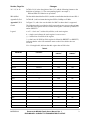
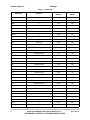
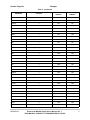
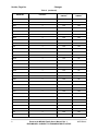
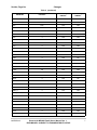
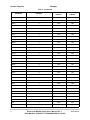
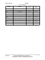
Addendum
MPC850R1UMAD
Rev. 1.4,10/2003
Errata to the MPC850 Family
User’s Manual, Rev . 1
This errata describes corrections to Revision 1 of the MPC850 Family Integrated
Communications Microprocessor User’s Manual (order number: MPC850UM, Rev. 1).
The MPC850 is a versatile, one-chip integrated microprocessor and peripheral combination.
The MPC850 includes a high-performance embedded PowerPC™ core and a communications
processor module (CPM).
1
Document Revision History
Table 1 provides a revision history for this errata addendum.
Table 1. Document Revision History
Revision Number
1.4
2
Substantive Change
Added new errata items from Section 1 (page 1-2), Section 27.7 (page 27-9),
Section 27.21 (page 27-3), Section 31.4.1.2 (page 31-9), Section 34.1 (page
34-2), Section 35.2.1 (page 35-4), and Appendix F (page F-2).
Document Errata
The section and page numbers of new errata items added since the last errata addendum
(6/14/02) are boldfaced.
Section/Page
Changes
1, 1-2
For the MPC850DSL part in Table 1-1, change “Time slot assigner,
SMC2 and I2C are not supported.” to the following:
“Time slot assigner and I2C are not supported.”
11.1.3.1, 11-3
Add the following note:
NOTE
The PLL loss of lock detection does not have a specification
for the detection threshold. Therefore it should be used
solely as a debug tool and not in production systems.
Characterization of the threshold value over temperature and
operating voltages has shown that the threshold can be
triggered when clock out to clock in phase differences are
1.8 ns. or more.
PRELIMINARY—SUBJECT TO CHANGE WITHOUT NOTICE
Section, Page No.
11.3.1.1, 11-9
Changes
In Figure 11-8, change the field description for bit 2 to BBE (boot burst enable) and
the field description for bit 15 to CLES (core little endian swap). Add the following
description to Table 11-3:
Table 11-3. Hard Reset Configuration Word Field Descriptions
Bits
Name
Description
2
BBE
Boot Burst Enable
0 The boot device does not support bursting.
1 The boot device does support bursting.
15
CLES
Core Little Endian Swap. Defines core access operation following reset.
0 Big Endian
1 Little Endian
14.2.2.3, 14-8
Replace Table 14-2 with the following:
Table 14-2. XFC Capacitor Values Based on PLPRCR[MF]
MF Range
Minimum Capacitance
1 ≤ (MF+1) ≤ 4 XFC = [(MF+1) x 425] - 125
(MF+1) > 4
15.4.1,15-9
XFC = (MF+1) x 520
Maximum Capacitance
Unit
XFC = [(MF+1) x 590] - 175
pF
XFC = (MF+1) x 920
pF
In Figure 16-6, BR0, add the following footnote:
Since the base address value is unknown at reset, program BR0 before
programming OR0 to ensure proper operation.
15.4.2, 15-11
Replace the text after Figure 16-7 with the following:
At reset, OR0 has specific default values and is read-only, as shown in
Figure 15-8. After reset, OR0 becomes R/W.
15.8.4, 15-55
Remove Section 15.8.4.1, “Address Incrementing for External Synchronous
Bursting Masters.”
27.7, 27-9
Add superscript number 2 after PADDR1_H, PADDR1_M, PADDR1_L,
TADDR_H, TADDR_M, and TADDR_L. Add the corresponding footnote 2 at the
end of Table 27-1 with the following statement: The address should be written in
little endian, not Motorola’s big endian format, that is, physical address
112233445566 should be written PADDR_L = 6655, PADDR_M = 4433, and
PADDR_H = 2211.The TADDR should be written in the same way as the PADDR.
27.21, 27-23
In step 26, change the last sentence to read, “Then write 0x000E to TxBD[Data...”
31.4.1.2, 31-9
In the last sentence of Example 1, change the order of the string for REV=1 to the
following: first j_nmlk__r_stuvlast
In the last sentence of Example 3, change the order of the string for REV=1 to the
following: firstr_stuv_ghij_klmnlast
34.1, 34-2
Inside the second bullet, add a footnote at the end of the sentence that states, “At
power on reset, port pins are not defined in any particular state until CLKOUT is
present for two clocks.”
34.3, 34-8
In Table 34-6, add RTS2 to PB18, PBPAR[DDn] = 1, and PBDIR[DRn] = 1.
2
Errata to the MPC850 Family User’s Manual, Rev . 1
PRELIMINARY—SUBJECT TO CHANGE WITHOUT NOTICE
MOTOROLA
Section, Page No.
Changes
34.5.1.2, 34-18
In Table 34-19, in the description of bits 3–15, add the following footnote to the
definition of setting to 1 (“The corresponding signal is an output.”):
PD8 and PD10 will function as open drain.
35.2.1, 35-4
The first bullet should reflect SPS=0, and the second bullet should reference SPS=1.
Appendix B, B-4
In Table B-1, add a column showing that USB is 24 Mbps at 25 Mhz.
Appendix F, F-2
In Figure F-1, add a line over the block for SMC2 to show that it is supported.
Global
The following table is provided to clarify/correct the power-on reset value of many
of the MPC850 registers and lists whether each register is affected by HRESET*
and/or SRESET*.
Legend:
x or X = “don’t care” in either bits, nibbles, or the entire register.
0 = a single zero indicates the entire register is reset to zeros.
( ) = isolates bits of a nibble of the register.
? = a don’t care for POR, but if this register is affected by HRESET* or SRESET*,
indicates that the value will remain the same as what it was before the reset
occurred.
NA = Not Applicable, indicates that this register has no POR value.
Table 2.
POR Value
Affected by
HRESET*
Affected by
SRESET*
SIUMCR
01200000
YES
NO
SYPCR
FFFFFF07
YES
NO
SWSR
0
YES
YES
SIPEND
0000xxxx
YES
YES
SIMASK
0000xxxx
YES
YES
SIEL
0000xxxx
YES
NO
SIVEC
(xx11)(11xx)xxxxxx
YES
YES
TESR
XXXX0000
YES
YES
SDCR
0
YES
NO
PBR0
x
NO
NO
POR0
x
NO
NO
PBR1
x
NO
NO
POR1
x
NO
NO
PBR2
x
NO
NO
POR2
x
NO
NO
PBR3
x
NO
NO
POR3
x
NO
NO
PBR4
x
NO
NO
POR4
x
NO
NO
REGISTER
MOTOROLA
Errata to the MPC850 Family User’s Manual, Rev . 1
PRELIMINARY—SUBJECT TO CHANGE WITHOUT NOTICE
3
Section, Page No.
Changes
Table 2. (continued)
POR Value
Affected by
HRESET*
Affected by
SRESET*
PBR5
x
NO
NO
POR5
x
NO
NO
PBR6
x
NO
NO
POR6
x
NO
NO
PBR7
x
NO
NO
POR7
x
NO
NO
PGCRA
0
YES
NO
PGCRBf
0
YES
NO
PSCR
x
NO
NO
PIPR
??00??00
YES
YES
PER
0
YES
YES
BR0
XXXXX(??00)0(000?)
YES
NO
OR0
00000FF4
YES
NO
BR1
XXXXXX(xx00)0
YES
NO
OR1
XXXXXXX(xxx0)
YES
NO
BR2
XXXXXX(xx00)0
YES
NO
OR2
XXXXXXX(xxx0)
YES
NO
BR3
XXXXXX(xx00)0
YES
NO
OR3
XXXXXXX(xxx0)
YES
NO
BR4
XXXXXX(xx00)0
YES
NO
OR4
XXXXXXX(xxx0)
YES
NO
BR5
XXXXXX(xx00)0
YES
NO
OR5
XXXXXXX(xxx0)
YES
NO
BR6
XXXXXX(xx00)0
YES
NO
OR6
XXXXXXX(xxx0)
YES
NO
BR7
XXXXXX(xx00)0
YES
NO
OR7
XXXXXXX(xxx0)
YES
NO
MAR
x
NO
NO
MCR
(xx00)0(x000)0(xxx0)X(00xx)X
YES
NO
MAMR
xx001000
YES
NO
MBMR
xx001000
YES
NO
MSTAT
0
YES
NO
MPTPR
0200
YES
NO
REGISTER
4
Errata to the MPC850 Family User’s Manual, Rev . 1
PRELIMINARY—SUBJECT TO CHANGE WITHOUT NOTICE
MOTOROLA
Section, Page No.
Changes
Table 2. (continued)
POR Value
Affected by
HRESET*
Affected by
SRESET*
MDR
x
NO
NO
TBSCR
0
YES
NO
TBREFA
x
NO
NO
TBREFB
x
NO
NO
RTCSC
00(000x)(000x)
YES
YES
RTC
x
NO
YES
RTSEC
x
NO
YES
RTCAL
x
NO
NO
PISCR
0
YES
NO
PITC
x
NO
NO
PITR
x
N/A
N/A
SCCR
0(000?)(?000)(0??0)0000
YES
NO
???0(0100)000
YES
YES
RSR
0
YES
YES
TBSCRK
x
YES
YES
TBREFAK
x
YES
YES
TBREFBK
x
YES
YES
TBK
x
YES
YES
RTCSCK
x
YES
YES
RTCK
x
YES
YES
RTSECK
x
YES
YES
RTCALK
x
YES
YES
PISCRK
x
YES
YES
PITCK
x
YES
YES
SCCRK
x
YES
YES
PLPRCRK
x
YES
YES
RSRK
x
YES
YES
I2MOD
0
YES
YES
I2ADD
x
NO
NO
I2BRG
FFFF
YES
NO
I2COM
0
YES
YES
I2CER
0
YES
YES
I2CMR
0
YES
YES
REGISTER
PLPRCR
MOTOROLA
Errata to the MPC850 Family User’s Manual, Rev . 1
PRELIMINARY—SUBJECT TO CHANGE WITHOUT NOTICE
5
Section, Page No.
Changes
Table 2. (continued)
POR Value
Affected by
HRESET*
Affected by
SRESET*
SDAR
x
NO
NO
SDSR
0
YES
YES
SDMR
0
YES
YES
IDSR1
0
YES
YES
IDMR1
0
YES
YES
IDSR2
0
YES
YES
IDMR2
0
YES
YES
CIVR
0
YES
YES
CICR
0
YES
NO
CIPR
0
YES
YES
CIMR
0
YES
YES
CISR
0
YES
YES
PADIR
0
YES
NO
PAPAR
0
YES
NO
PAODR
0
YES
NO
PADAT
x
NO
NO
PCDIR
0
YES
NO
PCPAR
0
YES
NO
PCSO
0
YES
NO
PCDAT
x
NO
NO
PCINT
0
YES
NO
PDDIR
0
YES
NO
PDPAR
0
YES
NO
PDDAT
x
NO
NO
TGCR
0
YES
YES
TMR1
0
YES
YES
TMR2
0
YES
YES
TRR1
FFFF
YES
YES
TRR2
FFFF
YES
YES
TCR1
0
YES
YES
TCR2
0
YES
YES
TCN1
0
YES
YES
TCN2
0
YES
YES
REGISTER
6
Errata to the MPC850 Family User’s Manual, Rev . 1
PRELIMINARY—SUBJECT TO CHANGE WITHOUT NOTICE
MOTOROLA
Section, Page No.
Changes
Table 2. (continued)
POR Value
Affected by
HRESET*
Affected by
SRESET*
TMR3
0
YES
YES
TMR4
0
YES
YES
TRR3
FFFF
YES
YES
TRR4
FFFF
YES
YES
TCR3
0
YES
YES
TCR4
0
YES
YES
TCN3
0
YES
YES
TCN4
0
YES
YES
TER1
0
YES
YES
TER2
0
YES
YES
TER3
0
YES
YES
TER4
0
YES
YES
CPCR
0
YES
YES
RCCR
0
YES
NO
RCTR1
NA
YES
YES
RCTR2
NA
YES
YES
RCTR3
NA
YES
YES
RCTR4
NA
YES
YES
RTER
0
YES
YES
RTMR
0
YES
YES
BRGC1
0
YES
NO
BRGC2
0
YES
NO
BRGC3
0
YES
NO
BRGC4
0
YES
NO
GSMR_L1
0
YES
YES
GSMR_H1
0
YES
YES
PSMR1
0
YES
YES
TODR1
0
YES
YES
7E7E
YES
YES
SCCE1
0
YES
YES
SCCM1
0
YES
YES
SCCS1
0
YES
YES
GSMR_L2
0
YES
YES
REGISTER
DSR1
MOTOROLA
Errata to the MPC850 Family User’s Manual, Rev . 1
PRELIMINARY—SUBJECT TO CHANGE WITHOUT NOTICE
7
Section, Page No.
Changes
Table 2. (continued)
POR Value
Affected by
HRESET*
Affected by
SRESET*
GSMR_H2
0
YES
YES
PSMR2
0
YES
YES
TODR2
0
YES
YES
7E7E
YES
YES
SCCE2
0
YES
YES
SCCM2
0
YES
YES
SCCS2
0
YES
YES
GSMR_L3
0
YES
YES
GSMR_H3
0
YES
YES
PSMR3
0
YES
YES
TODR3
0
YES
YES
7E7E
YES
YES
SCCE3
0
YES
YES
SCCM3
0
YES
YES
SCCS3
0
YES
YES
GSMR_L4
0
YES
YES
GSMR_H4
0
YES
YES
PSMR4
0
YES
YES
TODR4
0
YES
YES
7E7E
YES
YES
SCCE4
0
YES
YES
SCCM4
0
YES
YES
SCCS4
0
YES
YES
SMCMR1
0
YES
YES
SMCE1
0
YES
YES
SMCM1
0
YES
YES
SMCMR2
0
YES
YES
SMCE2
0
YES
YES
SMCM2
0
YES
YES
SPMODE
0
YES
YES
SPIE
0
YES
YES
SPIM
0
YES
YES
SPCOM
0
YES
YES
REGISTER
DSR2
DSR3
DSR4
8
Errata to the MPC850 Family User’s Manual, Rev . 1
PRELIMINARY—SUBJECT TO CHANGE WITHOUT NOTICE
MOTOROLA
Section, Page No.
Changes
Table 2. (continued)
POR Value
Affected by
HRESET*
Affected by
SRESET*
PIPC
0
YES
NO
PTPR
0
YES
NO
PBDIR
xxx(xx00)0000
YES
NO
PBPAR
xxx(xx00)0000
YES
NO
PBODR
0
YES
NO
PBDAT
x
YES
YES
SIMODE
0
YES
YES
SIGMR
0
YES
NO
SISTR
0
YES
NO
SICMR
0
YES
YES
SICR
0
YES
NO
SIRP
0
YES
YES
REGISTER
MOTOROLA
Errata to the MPC850 Family User’s Manual, Rev . 1
PRELIMINARY—SUBJECT TO CHANGE WITHOUT NOTICE
9
Section, Page No.
Changes
THIS PAGE INTENTIONALLY LEFT BLANK
10
Errata to the MPC850 Family User’s Manual, Rev . 1
PRELIMINARY—SUBJECT TO CHANGE WITHOUT NOTICE
MOTOROLA
Section, Page No.
Changes
THIS PAGE INTENTIONALLY LEFT BLANK
MOTOROLA
Errata to the MPC850 Family User’s Manual, Rev . 1
PRELIMINARY—SUBJECT TO CHANGE WITHOUT NOTICE
11
HOW TO REACH US:
USA/EUROPE/LOCATIONS NOT LISTED:
Motorola Literature Distribution
P.O. Box 5405, Denver, Colorado 80217
1-480-768-2130
(800) 521-6274
JAPAN:
Motorola Japan Ltd.
SPS, Technical Information Center
3-20-1, Minami-Azabu Minato-ku
Tokyo 106-8573 Japan
81-3-3440-3569
Information in this document is provided solely to enable system and software implementers to use
Motorola products. There are no express or implied copyright licenses granted hereunder to design
ASIA/PACIFIC:
or fabricate any integrated circuits or integrated circuits based on the information in this document.
Motorola Semiconductors H.K. Ltd.
Silicon Harbour Centre, 2 Dai King Street
Tai Po Industrial Estate, Tai Po, N.T., Hong Kong
852-26668334
Motorola reserves the right to make changes without further notice to any products herein.
Motorola makes no warranty, representation or guarantee regarding the suitability of its products
for any particular purpose, nor does Motorola assume any liability arising out of the application or
use of any product or circuit, and specifically disclaims any and all liability, including without
TECHNICAL INFORMATION CENTER:
limitation consequential or incidental damages. “Typical” parameters which may be provided in
(800) 521-6274
Motorola data sheets and/or specifications can and do vary in different applications and actual
HOME PAGE:
performance may vary over time. All operating parameters, including “Typicals” must be validated
for each customer application by customer’s technical experts. Motorola does not convey any
www.motorola.com/semiconductors
license under its patent rights nor the rights of others. Motorola products are not designed,
intended, or authorized for use as components in systems intended for surgical implant into the
body, or other applications intended to support or sustain life, or for any other application in which
the failure of the Motorola product could create a situation where personal injury or death may
occur. Should Buyer purchase or use Motorola products for any such unintended or unauthorized
application, Buyer shall indemnify and hold Motorola and its officers, employees, subsidiaries,
affiliates, and distributors harmless against all claims, costs, damages, and expenses, and
reasonable attorney fees arising out of, directly or indirectly, any claim of personal injury or death
associated with such unintended or unauthorized use, even if such claim alleges that Motorola was
negligent regarding the design or manufacture of the part.
Motorola and the Stylized M Logo are registered in the U.S. Patent and Trademark Office.
digital dna is a trademark of Motorola, Inc. The described product contains a PowerPC processor
core. The PowerPC name is a trademark of IBM Corp. and used under license. All other product
or service names are the property of their respective owners. Motorola, Inc. is an Equal
Opportunity/Affirmative Action Employer.
© Motorola, Inc. 2003
MPC850R1UMAD