1
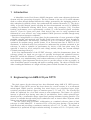
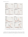
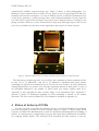
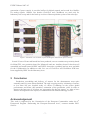
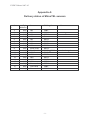
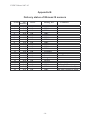
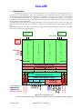
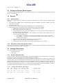
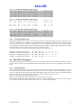
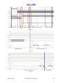
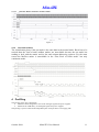
EUDET-Memo-2007-45 Status of pixel sensors for the demonstrator phase of EUDET beam telescope Wojciech Dulinski1 December 05, 2007 Abstract A general purpose beam telescope of new generation has been constructed and tested. All reference planes of the telescope are based on CMOS Monolithic Pixel Sensors (MAPS), fabricated for this application using AMS 0.35 µm OPTO process. Some of the sensors have been thinned down to about 50 µm, using commercially available post-processing. Present delivery status of the sensors is given in this report. It includes also the status of auxiliary electronics PCBs and the User Manual of MimoTEL, the standard reference sensor for the Telescope Demonstrator Phase. 1 IPHC, Strasbourg, France -1- EUDET-Memo-2007-45 1 Introduction A Monolithic Active Pixel Sensor (MAPS) integrates, on the same substrate, the detector element with the processing electronics. The key element is the use of N-well/P-substrate diode to collect through thermal diffusion the charge generated by the impinging particle in thin, undepleted (epitaxial) silicon layer underneath the readout electronics [1]. The device ability to provide charged particle tracking has been demonstrated on series of MIMOSA (standing for Minimum Ionizing MOS Active sensor) chip prototypes [2-4]. Excellent tracking performances were experimentally verified [5], with measured spatial resolution down to 1.5µm for 20µm pixel pitch. Such devices may now be easily optimized and fabricated in a cost effective way, using standard CMOS processes available through many commercial microelectronics companies. The idea of using MAPS as a sensor plane for the construction of a new generation of high precision, portable and equipped with flexible DAQ beam telescopes has been brought by EUDET Collaboration. The telescope, consisting of up to six reference planes, should be optimized for medium energy particle beams, as an electron beam line at DESY (6 GeV maximum). A dedicated study was performed to understand the position resolution in the telescope, in order to optimize its performance by choice of the best plane setup. The approach is based on novel analytical track fitting method, taking into account multiple Coulomb scattering effects [6]. In the first implementation of the EUDET telescope, called the demonstrator phase, the reference planes are based on two types of specially developed and optimized sensors: MimoTEL (called also Mimosa17) and Mimosa18 (known as a high resolution tracker). In both of them, very standard analog serial readout architecture of pixel has been chosen. From the beginning a great importance has been given to provide sensors as thin as possible, in order to minimize particle scattering and improve tracking quality. The choice of MAPS shall allow reaching the thickness of a single reference plane of much less than 100 µm of silicon. 2 Engineering run AMS-0.35 µm OPTO The pixel sensors for the telescope have been fabricated using AMS 0.35 OPTO process. The AMS-0.35µm OPTO process has been chosen for several reasons. It is an advanced mixed-signal CMOS process, providing four metal layers, two polysilicon layers, highresistivity polysilicon and two types of transistor gates (3.3 V and 5 V). The N-well/p-epi diodes are optimized for a low dark current at room temperature. The feature of a special interest is epitaxial layer having more than 10 µm thickness. Such a thick epitaxial layer should provide a comfortable charge signal from passing minimum ionizing particles. The process is available through multi-project submission runs at Austria Micro Systems which allows easy and cheap prototyping. The first sensor used by EUDET collaboration as a standard reference plane of their telescope is called MimoTEL. It consists of 256 x 256 pixel array having a 30 µm pitch in both direction and providing a continuous sensitivity area of 7.6 x 7.6 mm2. The other one (Mimosa18) is optimized for high resolution tracking. It consists of 512 x 512 pixels, with a -2- EUDET-Memo-2007-45 pixel pitch of 10 µm. A continuous tracking sensitive area with this device is of 5 x 5 mm2. In both sensors, a simple read out architecture is used (Fig.3). It consists of a 2-transistor pixel cell (half of a source follower plus a readout selection switch) connected to the charge collecting Nwell diode, continuously biased by another diode (forward biased) implemented inside charge sensing Nwell. The size of the sensing Nwell diode is of 4.4 x 3.4 µm, close to the minimum size required by the DRC rules of this process. Figure 1. Pixel circuit of sensors for the EUDET demonstrator phase beam telescope. The signal information from each pixel is serialized by a circuit (one per sub-array), which can withstand up to a 25 MHz readout clock frequency. This provides respectively for the MimoTEL and Mimosa18 a full frame readout time of 800 µs and 3 ms (with four parallel outputs present in both). In this architecture, the frame readout time is equal to the signal integration window. Information from two consecutive frames was read out: one frame before and one frame after each trigger. A data analysis based on the correlated double sampling (CDS) method was used for hit reconstruction. Mimosa16 Mimosa16 Latchup ADC ADC MyMap TestStruct MimoTEL Imager10µ Imager12µ MimoStar3 Figure 2. Layout of the single reticle from June 2006 IPHC engineering submission, containing several MAPS prototypes for different applications. The MimoTEL and the high resolution tracker (Mimosa18, called also Imager10µ) was part of an engineering run submitted by IPHC in June 2006. Figure 4 shows the layout of a single reticle (2 x 2 cm2 silicon area) from this submission, which contains several other sensors. The biggest one (MimoSTAR3, 320 x 640 pixel array, 30 µm pitch) is a prototype devoted for microvertex detector upgrade of the STAR experiment at RHIC (Brookhaven National Laboratory). Two types of wafers were used for this engineering submission: a “standard” wafers with 14 µm epitaxy and an “experimental” wafers with 20 µm epitaxy. To our knowledge, it is the thickest epitaxy layer available through commercial CMOS process. -3- EUDET-Memo-2007-45 3 Status of the delivery and tests of sensors Immediately after reception of six wafers from AMS at the and of October 2006, two wafers (one with 14 µm epitaxy and one with 20 µm epitaxy) has been diced and chips bonded to the readout PCBs (proximity boards). Each sensor was electrically tested in the laboratory prior to the high-energy particles tracking tests. The standard calibration procedure using 5.9 keV X-rays from a 55Fe source has been applied in order to measure basic parameters of the sensor. Equivalent noise charge (ENC) was found to be equal to 15 ± 1 electrons (10 ± 1 electrons) at room temperature, for the signal integration time of 1 ms (4 ms) respectively for MimoTEL and Mimosa18. A dark current, measured directly (MimoTEL) or estimated from the measured temperature dependence of the ENC (Mimosa18) of the sensing diode in this condition is of few dozens fA (MimoTEL) and less than 0.5 fA (Mimosa18). Only in case of MimoTEL, the corresponding shot noise contributes substantially to the thermal noise of the input transistor. The difference in dark current between two devices comes from the difference in design (layout) of the diode: it is a standard Nwell diode in case of Mimosa18 and radiation-tolerant diode in case of MimoTEL. Charge collection efficiency from epitaxy has been studied as function of cluster size and was found very different for two types of wafers (Figure 3). This is in particular the case of seed (central) pixel of a cluster, where the observed peak position from X-rays photons converted in epitaxy is substantially lower for 20 µm epitaxy type. This effect will severely limit expected increase of a signal charge from minimum ionizing particles traversing thicker epitaxy layer. During calibration phase of the Mimosa18 prototype, a new feature of X-rays spectrum was observed. It consists of characteristic double-peak (in addition to the third small peak at the right, corresponding to full charge collection), clearly visible in case of 2x2 and 3x3 clusters. This double-peak is much more pronounced in case of 20 µm epitaxy. The explanation for this effect is still to be found. During this phase of testing, it was found that the foundry by mistake didn’t implement one of required layer, high resistivity polysilicon. This missing layer has no influence on Mimosa18; it has not been applied in that sensor. For MimoTEL a small modification on PCB was required in order to provide one additional reference voltage, impossible to generate internally without high resistivity polysilicon. In order to correct the mistake, another production run was started at AMS in February 2007, with six wafers delivered in April. This run is referenced as “2007 submission”. After testing in laboratory, the telescope sensors has been intensely studied during 2007 at high energy beams at DESY and at CERN. The results, not discussed in this report, have been already presented and published [7, 8]. -4- EUDET-Memo-2007-45 a. b. Figure 3. Distribution of collected charge generated by 5.9 keV photons as a function of cluster size, for two types of epitaxial wafers for MimoTEL sensor (a) and for Mimosa18 sensor (b). The thickness of the sensors as delivered by the foundry is of 700 µm, not very optimum from the point of view of application for medium energy particle tracking. Therefore, several reticles from one of the delivered wafers were thinned down to less than 100 µm, using -5- EUDET-Memo-2007-45 commercially available post-processing step. Figure 4 shows a micro-photography of a Mimosa18 sensor thinned down to about 50 µm, glued on top of supporting PCB and wire bonded to the interface electronics. As seen on bottom picture, an internal mechanical stress of the device generates a visible bowing effect, with estimated amplitude of more than 100 µm. This effect is expected to be largely removed by more adequate choice of tooling for the gluing operation. However, for the construction of large area ultra-light objects, like several tens of sq. cm ladders for any microvertex application, this may be of serious concern. Figure 4. Mimosa18 thinned down to 50 µm, mounted and wire bonded on supporting PCB. The laboratory test phase was also very useful for the estimation of sensor production yield. In fact, out of 18 MimoTELs and out of 20 Mimosa18 assembled and tested sensors (including two M18 devices thinned down to 50 µm) all were found to be fully functional. Among MimoTELSs two sensors were showing important amount of dead pixels. In case of all assembled Mimosa18, the number of dead pixels was always smaller than 0.1%. Appendix_A and Appendix_B show present status of all assembled chips. Appendix_C presents a picture of Mimosa18 mounted on PCB (including a scheme of its readout direction). The first version of MimoTEL User Manual is included as Appendix_D. 4 Status of delivery of PCBs In order to be able to assemble the telescope set-up, a set of PCB (Printed Circuit Board) has been developed. It consists of several elements, shown in Figure 5. The proximity board (separate for MimoTEL and Mimosa18) is used for mechanical mounting and wire bonding of sensors. It contains passive components for power and control lines stabilization and buffers for outgoing analog signals. The Auxiliary PCB (common for both sensors) is used for -6- EUDET-Memo-2007-45 generation of power supply, it provides buffers for digital controls and second level buffers for analog signals. Another two boards (ClockTree and ClockRoot) are used only for laboratory test set-up and for the back-up version of data acquisition system of the telescope. Figure 5. Schematic view of PCBs required building the demonstrator phase telescope. In total 30 sets of front-end boards has been produced; one set contains one proximity board for MimoTEL, one proximity board for Mimosa18 and one Auxiliary board. It has been all assembled and tested between IPHC and DESY electronics workshop and are now available for the Collaboration. In addition to this, five sets of ClockTree and ClockRoot PCB have been supplied by IPHC for the laboratory tests. 5 Conclusion Production, assembling and delivery of sensors for the demonstrator went quite smoothly and is by now almost finished. The only on-going activity is thinning of sensors to less than 100 µm, detailed study of effects of thinning on the sensor global performance and better (full statistics) estimation of the production yield. In order to improve the later one (it is below our expectation for the big sensor), we plan to have intense investigation of the layout, in collaboration with AMS technology service. Acknowledgement This work is supported by the Commission of the European Communities under the 6th Framework Program “Structuring the European Research Area”, contract number RII3026126. -7- EUDET-Memo-2007-45 References 1. B. Dierickx, G. Meynants, D. Scheffer, “Near 100% fill factor CMOS active pixel”, in Proc. of the IEEE CDD&AIS Workshop, Brugge, Belgium, 5-7 June. 1997. 2. R. Turchetta, J. D. Berst, B. Casadei, G. Claus, C. Colledani, W. Dulinski et al. “A Monolithic Active Pixel Sensor for Charged Particle Tracking…”, Nucl. Instrum. Methods, vol. A458, pp. 677-689 3. G. Deptuch, J.D. Berst, G. Claus, C. Colledani, W. Dulinski, U. Goerlach, Yu. Gornushkin, Y. Hu, D. Husson, G. Orazi, R. Turchetta “Design and Testing of Monolithic Active Pixel Sensors for Charged Particle Tracking”, IEEE Trans.Nucl.Sci., Vol. 49, No 2 (2002) 601 4. G. Deptuch, G. Claus, C. Colledani, M. Deveaux, A. Gay, W. Dulinski, Yu. Gornushkin, Ch. Hu-Guo and M. Winter “Development of monolithic active pixel sensors for charged particle tracking”, Nucl. Instrum. Methods, vol. A511, pp. 240-249 5. W. Dulinski, J.-D. Berst, A. Besson, G. Claus, C. Colledani, G. Deptuch, M. Deveaux, A. Gay, D. Grandjean, Y. Gornushkin, A. Himmi, Ch. Hu, J.-L. Riester, I. Valin and M. Winter “CMOS Monolithic Active Pixel Sensors for Minimum Ionizing Particle Tracking Using Non-Epitaxial Silicon Substrate”, IEEE Trans.Nucl.Sci., Vol. 49, No 2 (2004) 601 6. A.F. Zarnecki “Analytical Track Fitting Method with Multiple Scattering of”, EUDET Collaboration Report-2007-1 7. A. Bulgheroni et al., “First Test Beam Results from the EUDET Pixel Detector”, IEEE NSS-MIC 2007 Conference Record, to be published 8. W. Dulinski et al., “Beam Telescope for Medium Energy Particles based on Thin, Submicron Precision MAPS”, IEEE NSS-MIC 2007 Conference Record, to be published -8- EUDET-Memo-2007-45 Appendix A: Delivery status of MimoTEL sensors Sensor # 1 2 3 4 5 6 7 8 9 10 11 12 13 14 15 16 17 18 Epi thickness 20 µ 20 µ 20 µ 20 µ 20 µ 20 µ 20 µ 20 µ 14 µ 14 µ 14 µ 14 µ 14 µ 14 µ 14 µ 20 µ 20 µ 20 µ Status Holding Inst. OK OK OK OK OK OK OK OK Pixel yield! Pixel yield! OK! OK! OK! OK! OK! Not tested Not tested Not tested IPHC IPHC IPHC Ferrara DESY DESY DESY DESY DESY DESYÆIPHC DESY DESY DESY DESY IPHC IPHC IPHC IPHC -9- Comments missing to be changed EUDET-Memo-2007-45 Appendix B: Delivery status of Mimosa18 sensors Sensor # 1 2 3 4 5 6 7 8 9 10 11 12 13 14 15 16 17 18 19 20 Epi thickness 20 µ 20 µ 20 µ 20 µ 20 µ 14 µ 14 µ 14 µ 14 µ 14 µ 14 µ 14 µ 14 µ 14 µ 14 µ 20 µ 20 µ 20 µ 20 µ 20 µ Status Holding Inst. OK OK OK OK OK OK OK OK OK OK OK OK OK OK OK OK OK OK OK OK IPHC IPHC IPHC IPHC DESY IPHC IPHC IPHC IPHC IPHC IPHC Frankfurt Frankfurt Frankfurt Oregon Oregon IPHC IPHC IPHC IPHC - 10 - Comments 6*1012 n/cm2 1013 n/cm2 Run 2007 Run 2007: thinned to 50µm Run 2007: thinned to 50µm EUDET-Memo-2007-45 Appendix C: - 11 - EUDET-Memo-2007-45 Appendix D: MimoTEL User Manual - 12 - MimoTEL User Manual C. Colledani, W. Dulinski, H. Himmi, Ch. Hu, I.Valin Institut de Recherches Subatomiques IN2P3-CNRS / ULP Strasbourg – France CENTRE NATIONAL DE LA RECHERCHE SCIENTIFIQUE INSTITUT NATIONAL DE PHYSIQUE NUCLEAIRE P HYSIQUE DES P ARTICULES ET DE MimoTEL Document history Version Date Description 1.0 Based on MimoStar2 Version October 2006 MimoStar chip family Version Date MimoTEL Submitted June 06 3L Submitted June 06 2 Submitted:June 05 1 Submitted July 04 October 2006 Description AMS 035 Opto Version, 256 x 256 pixels, Parallel outputs AMS 035 Opto Version, 640 x 320 pixels, Serial outputs AMS 035 Opto Version, 128 x 128 pixels TSMC 025 Version MimoTEL User Manual MimoTEL 1 2 Introduction ........................................................................................................................ 3 Control Interface ................................................................................................................ 4 2.1 JTAG Instruction Set.................................................................................................. 4 2.2 JTAG Register Set...................................................................................................... 5 2.2.1 Instruction Register ............................................................................................ 5 2.2.2 Bypass Register .................................................................................................. 5 2.2.3 Boundary Scan Register ..................................................................................... 5 2.2.4 ID_CODE Register ............................................................................................ 5 2.2.5 RO_Mode Register0........................................................................................... 5 2.2.6 DIS_COL Register ............................................................................................. 6 2.2.7 BIAS_DAC Register .......................................................................................... 6 3 Running MimoTEL ............................................................................................................ 7 3.1 After reset................................................................................................................... 7 3.2 Biasing MimoTEL...................................................................................................... 7 3.3 Setting the Readout_Mode Register........................................................................... 8 3.4 Readout....................................................................................................................... 8 3.4.1 Signal protocol ................................................................................................... 8 3.4.2 Successive frames and resynchronisation .......................................................... 8 3.5 Analogue Data Format ............................................................................................... 8 3.5.1 Normal mode data format .................................................................................. 8 3.5.1.1 Format of the analogue ouput Asgl<3> ......................................................... 8 3.5.1.2 Format of the analogue ouput Asgl<2> ......................................................... 9 3.5.1.3 Format of the analogue ouput Asgl<1> ......................................................... 9 3.5.1.4 Format of the analogue ouput Asgl<0> ......................................................... 9 3.5.2 Test mode data format........................................................................................ 9 3.6 MimoTEL Chronogram.............................................................................................. 9 3.6.1 Normal Readout ................................................................................................. 9 3.6.1.1 Alternate Mxfirst signal for normal readout ................................................ 11 3.6.2 Test mode readout ............................................................................................ 11 4 Pad Ring ........................................................................................................................... 11 4.1 MimoTEL Pad Ring and Floor Plan View............................................................... 12 4.2 Pad List..................................................................................................................... 13 October 2006 MimoTEL User Manual 2 MimoTEL 1 Introduction MimoTEL, the third version of the MimoStar family, has been designed in C35B4O1, the AMS 0.35 µm opto process. Like MimoStar 1 and 2, it is a Monolithic Active Pixel Sensor prototype dedicated to vertex particle tracking in the EUDET telescope. The matrix is composed by 256 x 256 pixels of 30 µm pitch and based on self biased diode architectures. It is organised in 4 matrices, or subframes, of 256 lines x 64 columns, accessed in parallel during the readout. The individual pixel architecture, should meet the radiation tolerance and the low leakage current requirements. The addressing of each subframe is sequential and starts from the upper left pixel up to the lower right pixel. The beginning of each subframe row is stamped by 2 dummy pixels acting as makers and having programmable levels. Each subframe has its own analogue serial output, a single ended voltage output buffer running up to 20 MHz which gives a readout time of 850µs/frame. Analog Supplies Digital Supplies gnd! Bias Tests vdd! Vdd_diode! vdda! Px<255:255> VREGAMP IPIX IKIMO gnd! Px<255:0> S u b f r a m e S u b f r a m e S u b f r a m e S u b f r a m e 3 2 1 0 ITEST Px<0:255> Px<0:0> Row Address Register <255:0> 4 Colum Address Reg<63:0> Current 2 Refence 1 A M x 1 A M x Bias Generators BIAS DAC Register<87:0> Disable Colum Register <255:0> RoMode <7:0> IDCODE ReadOut Controller CKRDP CKRDN SYNC RSTB TDO TDI TMS TCK Asgl2 Power Supplies CMOS Signals LVDS Signals Analogue Signals Asgl3 JTAG Controller RSTMK SSYNC MXFIRST LASTCOL LASTROW CK20M BSR <9:0> 2 2 1 A M x 1 A M x Asgl0 2 Asgl1 4 A-Mux 64 to 2 MimoTEL functional view Does not correspond to the floorplan; neither for the core, neither for the pad ring October 2006 MimoTEL User Manual 3 MimoTEL MimoTEL is very simple to operate: • Power On Reset or Reset on the RSTB pad • Setup of the chip It is performed with programmable registers accessed via an embedded slow control interface. It consists to: • Load the DACs which bias the analogue blocks • If necessary, load the ReadOut Register with a specific configuration. The default setup on power on reset allows a normal readout once the biases have been set. • Readout of the chip • The readout starts when the input "SYNC" token has its falling signal sampled by the LVDS readout input clock CKRD . It happens at the first rising edge of the 20MHz clock which follows the SYNC falling edge. • After a latency of 4 input clock cycles, the analogue signals appear on the output buffers • Digital maker outputs are available for the control of the readout process • Pixels are sequentially read out in a specific order explained later in the document • Successive pixel frames are read until the readout clock is stopped A frame resynchronisation can be performed at any time by setting up the "SYNC" token again. 2 Control Interface The control interface complies with the Boundary Scan, JTAG, IEEE 1149.1 Rev 1999 standard. It allows the access to the internal registers of the chip like the bias register and the readout mode selection register. On Power-On-Reset, an internal reset for the control interface is generated. The finite state machine of the Test Access Port (TAP) of the controller enters in the Test-Logic-Reset state and the ID register is selected. 2.1 JTAG Instruction Set The Instruction Register of the JTAG controller is loaded with the code of the desired operation to perform or with the code of the desired data register to access. Instruction EXTEST HIGHZ INTEST CLAMP SAMPLE_PRELOAD ID_CODE BIAS_GEN DIS_COL NU1 NU2 NU3 NU4 NU5 NU6 NU7 NU8 NU9 NU10 NU11 NU12 RO_MODE1 RO_MODE0 BYPASS October 2006 5 Bit Code16 01 02 03 04 05 0E 0F 10 11 12 13 14 15 16 17 18 19 1A 1B 1C 1D 1E 1F Selected Register BSR BYPASS BSR BYPASS BSR ID register BIAS register Disable Columns Read Out Mode1 Read Out Mode0 BYPASS Notes JTAG mandatory instruction JTAG optional instruction JTAG optional instruction JTAG optional instruction JTAG mandatory instruction JTAG optional instruction User instruction User instruction Reserved, Not Used Reserved, Not Used Reserved, Not Used Reserved, Not Used Reserved, Not Used Reserved, Not Used Reserved, Not Used Reserved, Not Used Reserved, Not Used Reserved, Not Used Reserved, Not Used Reserved, Not Used User instruction User instruction JTAG mandatory instruction MimoTEL User Manual 4 MimoTEL 2.2 JTAG Register Set JTAG registers are implemented with a Capture/Shift register and an Update register. JTAG standard imposes that the last significant bit of a register is downloaded/shifted first. Register Name INSTRUCTION REG BYPASS BSR ID_CODE BIAS_GEN (11 DACs) DIS_COL RO_MODE1 RO_MODE0 NU1, …, NU12 Size 5 1 9 32 88 256 8 8 0 Access R/W R Only R/W R Only R/W R/W R/W R/W Notes Instruction Register Fixed pattern Previous value shifted out during write Previous value shifted out during write Previous value shifted out during write Previous value shifted out during write Not implemented. For future use 2.2.1 Instruction Register The Instruction register is a part of the Test Access Port Controller defined by the IEEE 1149.1 standard. The Instruction register is 5 bits long. On reset, it is set with the ID_CODE instruction. When it is read the 2 last significant bits are set with the markers specified by the standard, the remaining bits contain the current instruction. X X X 1 0 2.2.2 Bypass Register The Bypass register consists of a single bit scan register. It is selected when its code is loaded in the Instruction register, during some actions on the BSR and when the Instruction register contains an undefined instruction. 2.2.3 Boundary Scan Register The Boundary Scan Register, according with the JTAG instructions, tests and set the IO pads. The BSR is 9 bits long and allows the test of the following input and output pads Bit # 8 7 6 5 4 3 2 1 0 Corresponding Pad LVDS CkRdP/CkRdN ASync SSync Ck5M Ck20M RstMk LastRow LastCol MxFirst Type Input Input Output Output Output Output Output Output Output Signal CkRd Sync SSync Ck5M Ck20M RstMk LastRow LastCol MxFirst Notes Resulting CMOS signal after LVDS Receiver Internal only, Not used 2.2.4 ID_CODE Register The Device Identification register is implemented is this third version. It is 32 bits long and has fixed value hardwired into the chip. When selected by the ID_CODE instruction or after the fixed value is shifted via TDO, the JTAG serial output of the chip. ID_CODE register value is 0xFFFF8001 2.2.5 RO_Mode Register0 The RO_Mode registers are 8 bits large; they allow the user to select specific features of the chip. MimoTEL use only the RO_Mode Register0. October 2006 MimoTEL User Manual 5 MimoTEL Bit # Bit Name 7 Not Used 6 Not Used 5 DisLVDS 4 SelMux 3 EnaGain3 2 1 0 Not used Not Used EnaTstCol Purpose Default value Disable LVDS, readout clock is not active 0 LVDS selected anymore. On MxFirst output pad, select the MuxFirst 1 MuxFirst Signal, active signal or the First_Pixel_of the Frame signal See § 3.4 Readout Select gain 3 for the serial differential output 0 Gain 5 buffer Test Mode: Select the 2 Test Levels, IVTEST1 0 Normal mode and IVTEST0, which emulate a pixel output 2.2.6 DIS_COL Register The DIS_COL register is 256 bit wide. The purpose of this register is to disable the column current sources if a short circuit is suspected on a specific column. During the readout, even if a current source is disabled the corresponding column is selected, i.e. no columns are skipped. Obviously, the signal of the corresponding pixel has no signification. The default value of the DIS_COL register is 0; it means that all current sources can be activated by the readout logic. Setting a bit to 1 disables the corresponding current source. The column <256> is on the left hand side while column<0> is on the right hand side. The organisation of the chip in 4 subframes of 64 columns has no matter to do with the DIS_COL register. 255 (Msb) DisCol<255> 0 (Lsb) DisCol<0> 2.2.7 BIAS_DAC Register The BIAS_DAC register is 88 bits large; it sets simultaneously the 11 DAC registers. As show bellow these 8-bit DACs set voltage and current biases. After reset, the register is set to 0, a value which fixes the minimum power consumption of the circuit. The current values of the DACs are read while the new values are downloaded during the access to the register. The image of the value of some critical biases can be measured on corresponding test pads. Bit range 87- 80 79- 72 DAC # DAC10 DAC9 71- 64 DAC8 63- 56 55- 48 DAC7 DAC6 47- 40 39- 32 31- 24 23- 16 DAC5 DAC4 DAC3 DAC2 15- 8 DAC1 7- 0 DAC0 October 2006 DAC Internal DAC purpose Name IKIMO External circuit monitoring I4PIX Pixel source follower bias. DAC with positive slope (0 to 255 µA; 1 µA step) V4TEST1 Test Level, emulates a pixel output. DAC with positive slope (0 to 2.55V; 10 mV step) V4TEST0 Idem V4REG3 Regulator voltage bias for the column amplifier (Gain 3 &5). DAC with negative slope ((3.3 to 0.75 V by step of 10 mV) V4REG2 Idem V4REG1 Idem V4REG0 Idem I4REGAMP Regulator current bias for column amplifier (G = 3 & 5) This DAC value is not very sensitive for test. DAC with positive slope (0 to 255 µA; 1 µA step) I4AMP Bias of column amplifier. DAC with positive slope (0 to 255 µA; 1 µA step) ISLOWBUFSE Bias of the single ended Output Buffers. DAC with positive slope (0 to 255 µA; 1 µA step) MimoTEL User Manual Corresponding Test Pad IKIMO IPIX No pad No pad VREGAMP No pad No pad No pad No pad No pad No pad 6 MimoTEL 3 Running MimoTEL The following steps describe how to operate the ASIC. 3.1 After reset On RSTB active low signal: • All BIAS registers are set to the default value, i.e. 0 • DIS_COL is set to 0, i.e. all columns are selected • RO_Mode is set to 0 • JTAG state machine is in the Test-Logic-Reset state • JTAG ID_CODE instruction is selected Then the bias register has to be loaded. The same has to be done for the RO_MODE0 and DIS_COL registers if the running conditions differ from defaults. Finally the readout can be performed either in normal mode or in test mode. 3.2 Biasing MimoTEL The BIAS_DAC register has to be loaded before operating the chip. The 11 DACs constituting this register are built with the same 8 bits DAC current generator which has a 1 µA resolution. Specific interfaces like current mirror for current sourcing or sinking and resistors for voltages, customise each bias output. The following table shows the downloaded codes which set the nominal bias. Internal DAC Name Resol Range Simulation Experimental(1) Code16 –Code10 Code16 - DacInterna Output ution Code10 l current- value µA IKIMO 64-100 100 1V 10 mV From 0 up to 2.55 V 0-0 I4PIX 1E-30 30 30 µA 1 µA From 0 up to 255 µA 1-1 V4TEST1 C3–195 195 1.95 V 10 mV From 0 up to 2.55 V FA-250 V4TEST0 B9–185 185 1.85 V 10 mV From 0 up to 2.55 V E6-230 V4REG 3 23–35 35 2.95 V 10 mV From 3.3 down to 0.75 V 80-128 V4REG 2 23–35 35 2.95 V 10 mV From 3.3 down to 0.75 V 80-128 V4REG 1 23–35 35 2.95 V 10 mV From 3.3 down to 0.75 V 80-128 V4REG 0 23–35 35 2.95 V 10 mV From 3.3 down to 0.75 V 80-128 I4REG1 21–33 33 33 µA 1 µA From 0 up to 255 µA 1-1 I4AMP 64–100 100 100 µA 1 µA From 0 up to 255 µA 3-3 ISLOWBUFSE 64–100 100 100 µA 1 µA From 0 up to 255 µA A-10 Note 1: The HRES ploysilicon, used in the bias block, is missing for this submission. Experimental values correspond to the recalculated parameters that allow nevertheless the chip be operated. A new submission of the chip is in progress. Bias synthetic block diagram Vrefn G=3&5 V Regulator I4PIX ISLOWBUFSE V4REGn + - I4REGAMP I4AMP * n = 0, 1, 2, 3 for 4 sub-matrices V4TEST1 + - October 2006 + - V4TEST0 MimoTEL User Manual 7 MimoTEL Note1: Vrefn ~= V4REGn – 1V 3.3 Setting the Readout_Mode Register If the desired operating mode does not correspond to the default one, set the Readout_Mode0 register following the §2.2.5 information. 3.4 Readout 3.4.1 Signal protocol Ones JTAG registers have been loaded, the readout of MimoTEL may initiate with the following signal protocol: • The readout clock CKRD is started. This allows the output pad CK20M to generate a 20 MHz clock. This clock follows the input. • The SYNC signal is set. • The readout starts at the first rising edge of CKRD after SYNC signal disappears. • Signal markers allow the monitoring of the readout and the analogue data sampling: o RstMk maker confirms that the internal reset of the readout logic is done. o SSync marker shows that the readout starts. o 4 extra CKRD clock cycles, after SYNC sampling, are necessary before the analogue signal of the first pixel appears on the output pad. o The MxFirst digital signal helps for a better sampling of the analogue output signals. The way it acts is set by the RO_Mode[4] bit. RO_Mode[4] = 0: MxFirst is active during the duration of the first maker of the frame RO_Mode[4] = 1: MxFirst is active on each pixel change on the analogue output i.e. it is a 20 MHz periodic signal. o LastCol is active when the last column of the current row is selected o LastRow is active when the last row of the frame is selected o Ck20M output shows the internal clock running as long as input clock is running. 3.4.2 Successive frames and resynchronisation Successive pixel frames are read until the readout clock is stopped. A frame resynchronisation can be performed at any time by setting up the "SYNC" token again. 3.5 Analogue Data Format Two types of signal can be generated • Normal pixel signal • Test signal. 3.5.1 Normal mode data format In order to improve the readout speed MimoTEL is organized 4 subframes. Each subframe has its own analogue serial output, a single ended voltage output buffer running up to 20 MHz. During the readout, the 4 subframes are accessed in parallel. For each subframe the addressing is done row by row, each pixel is accessed sequentially from the left side to right side. Each row contains 2 makers (acting as dummy pixels), and 64 active pixels. One can use the adjustable level of the 2 makers as a pattern recogniser. If the pixel coordinate format is specified as Px<Line, Column>, then for each subframe, the upper left pixel is Px<255, 63> while the lower right is Px<0, 0> and the makers of each beginning row are named Mk1 and Mk0. Thus the 4 parallel outputs generate respectively the following stream formats: 3.5.1.1 Format of the analogue ouput Asgl<3> Mk1, Mk0, Px<255,255>, Px<255,254>,. . ., Mk1, Mk0, Px<254,255>,.Px<254,254>,. . ., . . . . . . . . . . . . . . . . . . . . . Mk1, Mk0, Px< 1,255>,.Px< 1,254>,. . ., Mk1, Mk0, Px< 0,255>,.Px< 0,254>,. . ., October 2006 Px<255,192> Px<254,192> . . . . . . Px< 1,192> Px< 0,192> MimoTEL User Manual 8 MimoTEL 3.5.1.2 Format of the analogue ouput Asgl<2> Mk1, Mk0, Px<255,191>, Px<255,190>,. . ., Mk1, Mk0, Px<254,191>,.Px<254,190>,. . ., . . . . . . . . . . . . . . . . . . . . . Mk1, Mk0, Px< 1,191>,.Px< 1,191>,. . ., Mk1, Mk0, Px< 0,191>,.Px< 0,191>,. . ., Px<255,128> Px<254,128> . . . . . . Px< 1,128> Px< 0,128> 3.5.1.3 Format of the analogue ouput Asgl<1> Mk1, Mk0, Px<255,127>, Px<255,126>,. . ., Mk1, Mk0, Px<254,127>,.Px<254,126>,. . ., . . . . . . . . . . . . . . . . . . . . . Mk1, Mk0, Px< 1,127>,.Px< 1,126>,. . ., Mk1, Mk0, Px< 0,127>,.Px< 0,126>,. . ., Px<255, Px<254, . . . . Px< 1, Px< 0, 3.5.1.4 Format of the analogue ouput Asgl<0> Mk1, Mk0, Px<255, 63>, Px<255, 62>,. . ., Mk1, Mk0, Px<254, 63>,.Px<254, 62>,. . ., . . . . . . . . . . . . . . . . . . . . . Mk1, Mk0, Px< 1, 63>,.Px< 1, 62>,. . ., Mk1, Mk0, Px< 0, 63>,.Px< 0, 62>,. . ., Px<255, 0> Px<254, 0> . . . . . . Px< 1, 0> Px< 0, 0> 64> 64> . . 64> 64> 3.5.2 Test mode data format During the test mode the pixel matrix is not anymore connected to the multiplexing electronic. In place of it, two test levels V4TEST1 (V1), V4TEST0 (V0) are available. They emulate two pixel level outputs. Actually these levels correspond to those of Marker 1 and Marker 0. They are adjustable via 2 DACs. Even and odd columns are alternatively connected to one of them. This pattern allows seeing the output signal changing and emulates the readout shift from one column of pixel to the other column of pixel. Thus the 4 parallel outputs generate respectively the following stream formats: Subframe 3, analogue ouput Asgl<3>: Subframe 2, analogue ouput Asgl<2>: Subframe 1, analogue ouput Asgl<1>: Subframe 0, analogue ouput Asgl<0>: 3.6 V1, V0, V1, V0, V0, V1, V0, V1, V0, V1, V0, V1, V1, V0, V1, V0, V1, V0, V1, V0, V0, V1, V0, V1, V0, V1, V0, V1, V1 V0 V1 V0 . . . . . . . . . . . . MimoTEL Chronogram The following chronograms describe typical access to the chip; Reset, JTAG download sequence and then the readout. This one starts with the initialisation phase followed by the successive row readouts as showed in the zoom. 3.6.1 Normal Readout Figure 1 show the beginning of a typical normal data readout mode. After Reset and JTAG settings, one can see the initialisation phase of the readout of the first pixel row. The LastCol signal is active meanwhile the last pixel of a row is read. The last row of the frame makes the LastRow signal to be active. One of the 4 parallel analogue outputs is showed. One can distinguish the 2 makers placed at the beginning of each row. Figure 2 is the zoom of the readout of the first row. Figure 3 is an enlargement of the transition from one row to the successive one. Figure 4 show the alternate option of the MxFirst signal. It is active only during the time the first maker appears i.e. just before the first pixel of the frame. This option is set via the RoMode register. October 2006 MimoTEL User Manual 9 MimoTEL Reset Jtag access Idle 1 rstrow readout + Init Successive row readouts Last row readout Figure 1 <3> Marker<0> Px<255,248> Px<255,254> Px<255,255> Px<255,253> Px<255,249> Px<255,247> Marker<1> 1 rst row readout phase Initialisation phase Figure 2 <3> Marker<0> Px<255,191> Px<255,192> Px<255,190> Px<255,254> Px<254,255> Px<255,253> Marker<1> End of 1 rst row readout 2 nd row readout Figure 3 October 2006 MimoTEL User Manual 10 MimoTEL 3.6.1.1 Alternate Mxfirst signal for normal readout Figure 4 3.6.2 Test mode readout The initialisation phase if the test mode is the same than in the normal mode. But it has to be noticed than the LastCol and LastRow makers are unavailable because the test mode has nothing to deal with the matrix and its line and column addressing registers. For the same reason the MxFirst maker is unavailable in the “First Pixel of frame mode” but only continuous mode. V0 V1 V0 V0 V1 V1 V1 V1 V0 V0 V0 V0 V1 V1 V1 V1 4 Pad Ring The pad ring of the chip is build with • Pads full custom designed for some of the analogue signals and power supplies • Pads from the AMS library for the digital signals and power supplies The pad ring is split in 6 functional independent parts. Each part has its own supply pads. October 2006 MimoTEL User Manual 11 MimoTEL 4.1 MimoTEL Pad Ring and Floor Plan View SubMx3 SubMx1 SubMx2 SubMx0 RdO-Cntl 20 DAC 1 P_A1 P_D1 P_A2 P_L P_D2 P_A3 75 Foundry submission information MimoTEL has been designed in AMS C35B4O1 CMOS 0.35 μm. The Process Design Kit V3.70 has been provided by CMP CAD tools are CADENCE DFII 5.0 with DIVA and ASSURA rules October 2006 MimoTEL User Manual 12 MimoTEL 4.2 Pad List Pad 1 2 3 4 5 6 7 8 9 10 11 12 13 Name IKIMO IPIX VREGAMP gnd Aout<3> gnd gnd gnd gnd ITEST vdda vdda vdda Pad ring segment 1 – P_A1 Pad General Function PadType APRIOP Analog I/O pad, 0 Ω serial APRIOP Analog I/O pad, 0 Ω serial APRIOP Analog I/O pad, 0 Ω serial Core logic and periphery cells supply AGNDALLP Direct Pad, no protections DIRECTPAD Core logic and periphery cells supply AGNDALLP Core logic and periphery cells supply AGNDALLP Core logic and periphery cells supply AGNDALLP Core logic and periphery cells supply AGNDALLP APRIOP Analog I/O pad, 0 Ω serial Analogue Pad Supply AVDDALLP Analogue Pad Supply AVDDALLP Analogue Pad Supply AVDDALLP Pad 14 15 16 17 18 19 20 21 22 23 24 25 26 27 28 29 30 Name RSTMK vddd vddd LastRow vddd LastCol vddd vddd CK20M gnd gnd MxFirst gnd Ssync gnd gnd Sync Pad ring segment – P_D1 Pad General Function PadType Tri-State Output Buffer, 2 mA BT2P Core logic and periphery cells supply VDD3RP Core logic and periphery cells supply VDD3RP Tri-State Output Buffer, 2 mA BT2P Core logic and periphery cells supply VDD3RP Tri-State Output Buffer, 2 mA BT2P Pad supplying the output buffers VDD3OP Pad supplying the output buffers VDD3OP Tri-State Output Buffer, 2 mA BT2P Pad supplying the output buffers GND3OP Pad supplying the output buffers GND3OP Tri-State Output Buffer, 2 mA BT2P Core logic and periphery cells supply GND3RP Tri-State Output Buffer, 2 mA BT2P Core logic and periphery cells supply GND3RP Core logic and periphery cells supply GND3RP CMOS Input Buffer ICP Function for the chip Readout Reset Marker 3.3 V 3.3 V Last Row Maker 3.3 V Last Column Marker 3.3 V 3.3 V 20 MHz Clock Out Ground Ground First pixel maker Ground periphery cells only Readout Synchro. Start Marker Ground periphery cells only Ground periphery cells only Readout Input token Name gnd gnd Aout<2> gnd vdda vdda vdd_diode vdd_diode vdd_diode vdda vdda gnd Aout<1> Pad ring segment – P_A2 Pad General Function PadType Core logic and periphery cells supply AGNDALLP Core logic and periphery cells supply AGNDALLP Direct Pad, no protections DIRECTPAD Core logic and periphery cells supply AGNDALLP Analogue Pad Supply AVDDALLP Analogue Pad Supply AVDDALLP Direct pad, no protections DIRECTPAD Direct pad, no protections DIRECTPAD Direct pad, no protections DIRECTPAD Analogue Pad Supply AVDDALLP Analogue Pad Supply AVDDALLP Core logic and periphery cells supply AGNDALLP Direct Pad, no protections DIRECTPAD Function for the chip Ground periphery & core Ground periphery & core Analogue data out Ground periphery & core 3.3 V 3.3 V Pixel Diode Bias, 3.3V Pixel Diode Bias, 3.3V Pixel Diode Bias, 3.3V 3.3 V 3.3 V Ground periphery & core Analogue data out Pad 31 32 33 34 35 36 37 38 39 40 41 42 43 October 2006 MimoTEL User Manual Function for the chip Gen Purpose DAC Output DAC Out, Test Purpose Only DAC Out, Test Purpose Only Ground periphery & core Analogue data out Ground periphery & core Ground periphery & core Ground periphery & core Ground periphery & core Internal Current Ref Source 3.3 V 3.3 V 3.3 V 13 MimoTEL 44 gnd 45 gnd Core logic and periphery cells supply Core logic and periphery cells supply AGNDALLP AGNDALLP Ground periphery & core Ground periphery & core Name gnd CKRN CKRP vdd Pad ring segment 3 – P_L Pad General Function PadType Function for the chip LVDS Pad Ground AGNDALLP Ground for LVDS Pad Full Custom Readout Clock Signal LVDS In LVDS In + LVDS Pad Supply AVDDALLP 3.3V for LVDS Pad Pad 50 51 52 53 54 55 56 57 58 59 60 61 62 63 64 65 66 Name vddd vddd RSTB vddd vddd TMS vddd vddd TDI gnd gnd TCK gnd gnd TDO gnd gnd Pad ring segment 2 – P_D2 Pad General Function PadType Core logic and periphery cells supply VDD3RP Core logic and periphery cells supply VDD3RP Schmitt-Trigger Input Buffer, Pull Up ISUP Core logic and periphery cells supply VDD3RP Core logic and periphery cells supply VDD3RP CMOS Input Buffer, Pull Up ICUP Pad supplying the output buffers VDD3OP Pad supplying the output buffers VDD3OP CMOS Input Buffer, Pull Up ICUP Pad supplying the output buffers GND3OP Pad supplying the output buffers GND3OP CMOS Clock Input Buffer, 2 mA ICCK2P Core logic and periphery cells supply GND3RP Core logic and periphery cells supply GND3RP Tri-State Output Buffer, 4 mA BT4P Core logic and periphery cells supply GND3RP Core logic and periphery cells supply GND3RP Function for the chip 3.3 V 3.3 V Asynchronous Active Low Reset 3.3 V 3.3 V JTAG Control Signal 3.3 V 3.3 V JTAG Control Signal Ground Ground JTAG Clock Ground Ground JTAG Serial Data Out Ground Ground Pad 67 68 69 70 71 72 73 74 75 Name vdda vdda vdda gnd Aout<0> gnd gnd gnd gnd Pad ring segment – P_A3 Pad General Function PadType Analogue Pad Supply AVDDALLP Analogue Pad Supply AVDDALLP Analogue Pad Supply AVDDALLP Core logic and periphery cells supply AGNDALLP Direct Pad, no protections DIRECTPAD Core logic and periphery cells supply AGNDALLP Core logic and periphery cells supply AGNDALLP Core logic and periphery cells supply AGNDALLP Core logic and periphery cells supply AGNDALLP Function for the chip 3.3 V 3.3 V 3.3 V Ground Analogue data out Ground Ground Ground Ground Pad 46 47 48 49 October 2006 MimoTEL User Manual 14