1
[GROUP 12 SENIOR DESIGN DOCUMENT SPRING 2013] April 29, 2013
1.
Executive Summary
The goal of this project was to develop an enhanced navigation experience that
goes beyond a simple two dimensional (2D) map, or turn by turn directions. To
do this augmented reality was used to add visual aids to the user experience in
order to more easily display directly to the user, the location of desired points of
interest, and a visual path of how to get there. Augmented reality was used to
overlay visual cues on top of what the user is seeing on their device. This
method ensures that the user can easily confirm that what they see on the map
directly conforms to the environment they see around them.
To implement this augmented reality setup, an application was developed that
integrated a 2D map interface, augmented reality navigation, Global Positioning
System (GPS) location tracking, and customization of points of interest options.
This application was installed into an electronic device that is portable, uses a
common hardware platform, and a common operating system (OS) foundation.
By building for an electronic device that uses common components and software
foundations, the developed navigation application will be eminently portable to
other electronic devices such as smart phones or tablets.
To design this electronic device, we began with a hardware development kit as a
foundation, and added any additional hardware functionality we needed in order
to achieve the goals of this project. By starting with a hardware and software
platform that is common to the industry, the sourcing of parts, design of the
software application and the ability to customize the design was made eminently
easier.
To prepare for this undertaking various hardware and software platforms were
investigated in order to determine what will best suit our needs. The general
design process began with an investigation into various operating system
platforms and their various strengths and weaknesses. Since the operating
system is what ties the application and hardware together, and to an extent
determines what hardware foundation is used, it was a natural place to start.
Once an operating system was chosen, the next step was to choose the
hardware platform to run it on. This was needed to be portable, expandable, and
easily customizable to enhance the user experience and provide sufficient
performance to support the software environment. Any hardware functionality
that was not in the chosen platform was designed and added in order to meet the
needs of this project. Application research and design was able to begin once
the hardware and software platform was selected.
The design team for this project is composed of two senior electrical engineering
students, and two senior computer engineering students.
The electrical
engineers focused on the hardware aspects of this project, which included
designing an expansion board that adds hardware functionality to the base
1
[GROUP 12 SENIOR DESIGN DOCUMENT SPRING 2013] April 29, 2013
hardware, providing a battery power supply to make the system portable. The
computer engineers will focus on the software aspects of this project, including
application development and integration into the OS environment and setting up
any low level communication between the hardware in the expansion board and
the hardware in the base device. They will also ensure proper OS to hardware
operation.
2.
Project Description
2.1.
Project Motivation and Goals
Navigation applications have often required that the user be able to understand
and interpret a 2D map, understand their location on a map, and be able to
identify significant landmarks identified on the map, such as cross streets,
buildings or terrain. Even after the user has accomplished this task, assistance
provided by the application to inform the user of where they need to go next on
the path to their destination have also been limited to a line on a 2D map, or
verbal step-by-step instructions. This is suitable for those who have a natural
sense of direction, or an aptitude for map reading, but can be difficult for lay
users. It can also be difficult for them to identify specified landmarks that are
often labeled with vague outlines.
The inherent difficulties on navigation with a 2D map that displays locations with
at best outlines of significant landmarks, or at worst a single point with a title are
easy to see. Users can have a difficult time identifying locations on a map
because they have no idea what the target destination is supposed to look like.
GPS navigation can be very helpful in informing the user of their current location
and direction of travel, but it can't point out to the user what they are looking for
or how it looks like.
Even turn by turn instructions can be of limited usefulness because the world we
live in does not lend itself to fit cleanly in a 2D X,Y space. Anyone who has
traveled in an urban environment, especially one that is built up from an older city
can understand the frustration of receiving an instruction to "Turn Right", and
there be two or three right turn options because the intersection has five or six
streets coming off it. Perhaps the intersection it multilevel, with one right turn
passing under an elevated roadway that also has an off ramp to the right to get
onto the elevated roadway.
These ambiguities can lead to lost time and frustration as the user is forced to
guess what the correct path is and determine through process of elimination
which one was correct. Signs can be unreliable as well, as they can be placed in
hard to notice locations, or be damaged or missing, thus making it difficult to
know if the user is at the correct cross street, or at the specified landmark that
designates their next turn to their destination.
2
[GROUP 12 SENIOR DESIGN DOCUMENT SPRING 2013] April 29, 2013
If a device could be designed and built that not only generated a path to a user’s
destination, but could actually highlight on the screen precisely what the user is
looking for, these issues could be resolved. Imagine a device that when the user
holds it up to the landscape they are looking at, the device draws virtual
information to its screen that directly super imposes onto what the use is seeing
in their landscape. This can enable the user to directly follow visual cues their
destination, and be able to precisely identify what it is they are looking for.
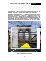
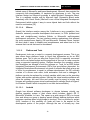
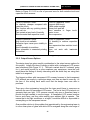
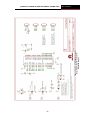
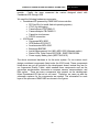
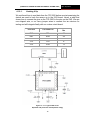
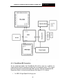
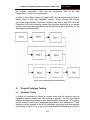
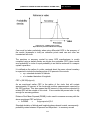
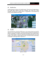
With a device like this (See Figure 2.1.1), even the most novice of user would be
able to follow the virtual image of say a line or arrow, without having to worry if
they passed the street or sidewalk that they were supposed to turn on. They
would not need to worry about identifying intermediate land marks along their
path that mark the location of their next turn. They also wouldn't need to
determine if they are heading the right direction every time they change heading.
Figure 2.1.1: Navigation Tablet Concept Idea
3
[GROUP 12 SENIOR DESIGN DOCUMENT SPRING 2013] April 29, 2013
Augmented reality can provide an enhanced navigation experience that
overcomes the difficulties mentioned above. The target groups for this enhanced
navigation are users who are both skilled, and unskilled with map reading and
navigation.
Unskilled users will benefit by being able to follow virtual
representations of the desired path, and without even needing to look at the map,
or know their current location, arrive at their desired destination. Skilled users
will find the points of interest functionality very useful in being able to mark on 2D
map locations that can be highlighted in the augmented reality space, thus
providing additional perspective as to distance and direction from the users
current location. This will also allow the user to easily share with others points of
interest that they too can see on their augmented reality setup.
This target group can also be expanded to today's war fighter. Often times
soldiers can find themselves operating in environments that don't offer easily
identifiable landmarks for them to maintain their bearings. Dense urban
environments, mountainous terrain, dense jungle and forest, can all conspire to
confuse soldiers as to their exact location, the location of their destination, and
any important areas around them. A tool that overlays digital information on top
of what they are seeing would be invaluable to instantly informing them of their
exact path, and providing perspective as to how far, and in what direction in
relation to what they are seeing is their objective. The ability to mark enemy
positions on a map, and then visually see those positions overlaid onto what they
are seeing would allow them to precisely locate hidden or difficult to see
locations.
The potential benefits and applications to the modern war fighter can be endless.
Whole areas could be marked as unsafe for things such as minefield locations,
ambush sights, and large numbers of hostiles. Combining this application with
automated visual processing could even allow the device to automatically
created landmarks of interest on the map, such as buildings that provide support
to the enemy effort.
Although this capability is beyond the scope of this project, the basic foundation
for a whole host of supplementary applications begins with an application that
provides live visual cues to the user, directly displaying optimal paths to their
destination over what they are seeing, landmarks of interests, and information
about those landmarks with the added ability to custom add those landmarks.
2.2.
Project Solution Goals
Keeping these target groups in mind, the engineering team designed and built a
portable tablet that will display augmented reality visuals (via software application
installed to the tablet) onto what the user is seeing. This can take several
possible forms, such as using the tablets built in camera to display video of what
the user is seeing on the screen, and then overlay a virtual image over it to show
the user additional information. Another method could be to make the tablets
screen transparent, so that the virtual images can be overlaid directly onto what
4
[GROUP 12 SENIOR DESIGN DOCUMENT SPRING 2013] April 29, 2013
the user is seeing. A final method would be to display the virtual images to
special goggles that contain built in screens that can be used to overlay the
virtual images into the user’s field of use. Ideally the implementation of this
navigation aid would be able to function using any of these methods.
This tablet was built onto a hardware platform that is common to other tablet
designs, such as those used for Android or IOS devices. By adopting one of the
popular hardware and software standards, the team was able to build a product
that can be widely used on all other similar devices. By using a common
platform with other devices the software implementation of the augmented reality
can be easily installed to other devices that share the same platform.
By using a tablet design that one can hold up to their line of sight with the
landscape and allow the software to draw visual cues over, the problems
mentioned in 2.1 can be overcome. A tablet design can present a large surface
to view virtual visual aids. It can be used to implement any of the possible three
forms mentioned above. Whenever the user needs to see where to do they can
simply lift up the tablet, which will automatically display visual clues about which
way to face, and overlay line and arrows about where to travel directly over what
they are seeing.
Designing for a tablet that is built around one of the popular development
packages, the navigation aid application could be scaled to work with smaller
devices such as smart phones. The attachment of visual goggles to the tablet
that display the same images seen on the tablet would even allow the user to
avoid having to hold the tablet with their hands, freeing them for other uses.
The goggles implementation is probably the best design solution since it allows
the users hands to remain free for task such as driving. For soldiers it would also
be the best implementation, since they are already overburdened with equipment
to carry and it can be integrated to the anti-ballistic glasses they already wear.
Goggles are only a form of display however, which can be plugged into any tablet
device and about the data shown on the tablet screen. The tablet still serves as
the foundation device in this setup, and thus the tablet will be the focus of design
efforts for this project.
In the end, transparent LCD panels proved to be unavailable, and thus could not
be used for this project. The group also didn’t want to dedicate budget resources
to purchase 3D goggles, and thus it was decided to implement the camera
combined with a normal LCD panel.
Once the group decided on the size, shape, and nature of the tablet, the
augmented reality was implemented in a software application designed to run on
the tablet design. This application is able to combine all of the elements of
traditional navigation applications, such as a 2D map, and step-by- step
5
[GROUP 12 SENIOR DESIGN DOCUMENT SPRING 2013] April 29, 2013
navigation, with 3D augmented reality that provides further visual information to
the user.
This application has two main areas of focus. The first involves using augmented
reality cues to tell the user exactly where to go when they are looking at the
tablet. In other words, a virtual pointer is overlaid live onto what the user is
seeing, so that they can follow it easily to their destination. By using a pointer on
what they are seeing, the user need not be able to interpret a map. They won't
need to be able to identify landmarks, such as streets, intersections, or buildings
along the path to their destination.
This implementation solves an inherent limitation of turn by turn instructions. The
augmented reality tablet highlights the exact path the user must follow. The user
will only need to follow the pointer, without needing to identify intermediate
landmarks to get to their destination. This also allows them to easily take the
exact path they must take, both locally and in the distance in front of them,
adding new perspective to the journey that they previously could only conjure up
in their mind with a flat 2D map.
The second main focus of this application will be to allow the user to add
landmark references to a 2D map.
Soldiers could use it to highlight enemy foxholes, or gun positions, or mark off
entire areas to avoid. It is one thing to mark on a map the location of a point of
interest; it is another completely to be able to see where it is in their field of view.
By having it displayed in their field of view, they will not waste time trying to
match the data they see on their 2D map with the field of view they see in front of
them. Instead all of the digital information of the 2D map can be directly
displayed on top of their view allowing them to instantly grasp any important
information.
2.3.
Project Requirements and Specifications
Starting with the application portion of this project and working back to the
hardware portion, the feature and performance requirements of this design will
need to satisfy the goals defined in 2.2.
The application will need to locate the user’s current location with a precision of
less than five meters in error in an outdoor environment. At that distance the
user should be to see their destination without difficulty. If this performance can
be improved upon, it may be possible to add extra functionality to enable a very
fine grain of point to point navigation, such as leading straight to the doorway of a
building.
The application will need to match the GPS's level of accuracy when overlaying
its virtual images over what the user is seeing. This means that visual cues,
such as lines representing the user’s path to destination, and arrows showing the
6
[GROUP 12 SENIOR DESIGN DOCUMENT SPRING 2013] April 29, 2013
required direction of travel must overlay accurately to the users visual plane.
This will apply equally to landmarks that the user chooses to identify on their
map. The level of accuracy achieved will directly translate into how small a
landmark the user chooses to identify. Highlighting the floor of a building
accurately, is much easier then highlighting a specific window. The same less
than five meter accuracy will be used.
Indoor navigation will be attempted, though GPS accuracy decreases noticeably
indoors, and may not prove feasible for time allowance of this project. However,
if indoor GPS navigation can be achieved reliably, then indoor room to room
navigation can be attempted. The device must be able to tell what floor it is on
when as it is moving through a building. A barometric sensor will be needed for
this purpose, so the tablet must integrate one.
To support the software requirements the tablet must integrate the necessary
sensors to feed the needed data to the application. This includes the already
mentioned barometric sensor for altitude detection, but it must also be able to
fully detect movement, changes in orientation and acceleration. This information
will not only be needed to activate the application when the user brings up the
tablet into their field of view, but will also be needed to help in determining the
users direction of travel, and their current facing when standing still. As such, the
tablet must contain a gyroscope, accelerometer, and compass.
This tablet must also be able to offer a level of computational performance
sufficient for computing not only the necessary navigational data, but also for
generating the 3D imagery necessary for the augmented reality portion of the
project. A graphics accelerator will thus be needed, as well as a powerful
enough CPU and large enough RAM to support the application.
The display method of this tablet will depend on a number of factors. The
simplest version that was mentioned in section 2.2 is to use the onboard camera
to record video and stream it to the screen in order to replicate what the user is
seeing in their plane of view. Then the virtual visual aids can be super imposed
onto the video stream. This method has the advantage of using standard
hardware that is commonly available.
The more advanced version is to use a transparent screen so that the user can
simply look through the tablet and allowing them to never have to take their eye
off of what they are looking at. It will also ensure that the perspective of the user
is not altered by the position of the camera in the device. However transparent
screens are still an experimental product and using one will depend mostly in
being able to acquire one. If one cannot be bought, then the simple method
mentioned above will be used.
Should time and budget permit, the use of goggles plugged into the tablet can be
explored and possible implemented as an additional feature for this project, this
7
[GROUP 12 SENIOR DESIGN DOCUMENT SPRING 2013] April 29, 2013
should not be considered a required goal of the project though, just a future
possible path to take the design in the future.
All of this hardware will need to fit into a chassis that a user can elevate to eye
level for a useful amount of time. Given the design group's limited manufacturing
abilities, a weight limit of no more than three pounds will be aimed for. In
accordance with this, a screen size no larger than ten inches will be used, but no
smaller than seven inches, in order to provide a comfortable user experience with
the tablets interface.
Naturally the design will need to integrate a battery in order to make the device
portable. Power consumption and efficiency is not a design priority for this
project, so a modest three hour battery life is being aimed for; in order to facilitate
final design testing which will take place in real world environments.
Given that UCF's Institute for Simulation and Training have generously agreed to
fund this project to the amount of $2,000; the final cost for parts and
manufacturing must not exceed this amount. If accomplished, this would prove
significant in and of itself, that an augmented reality navigation tablet can be
designed and built using standard off the shelf parts for $2,000 or less.
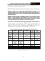
Project minimum Performance goals verses Real Tablet Products
.75 lbs
10.81x6.77x0.3
7
1.5 lbs
Kindle
Fire HD 7
7.6x5.4x0.
4 in
.87 lbs
7.9 in
7 in
10.6 in
7 in
7 in
4490 mAh
4325 mAh
8200 mAh
4400 mAh
2200 mAh
Apple A5
Tegra 3
Tegra
TI OMAP
4460
Light,
accelerometer
, gyro,
compass
Light,
accelerometer
, gyro,
compass
Light,
accelerometer,
gyro, compass
None
TI OMAP
4460
Light,
accelerometer
, gyro,
compass,
barometer
iOS 6
Android 4.1
Windows 8 RT
YES
YES
YES
YES
YES
YES
NO
YES
YES
iPad Mini
Size
Weight
Screen
Size
Battery
Life
Processo
r
Sensors
Operating
system
GPS
Bluetooth
Wifi
7.87x5.3x0.28
in
.68 lbs
Nexus 7
Surface RT
7.8x4.72x0.41
Figure 2.3.1: Tablet Comparisons
8
Android
Forked
NO
YES
YES
Project
Tablet
11x8.5x3.2
4
Android 4.0.3
YES
YES
YES
[GROUP 12 SENIOR DESIGN DOCUMENT SPRING 2013] April 29, 2013
In summation, at a minimum, this project will accomplished the construction of a
tablet computer not weighing more than three pounds, with a screen no larger
than ten inches, and a three hour battery life. This tablet will power the new
navigation application that will provide an augmented reality experience to users
in order to aid them in navigating to desired destinations, and in highlighting
points of interest relevant to their needs. These design goals should be
considered a minimum goal. Figure 2.3.1 above compares these modest design
goals against shipping tablet products.
3.
Research Related to Software and Hardware Design
3.1.
Software Resources Research: Android vs iOS vs WP8
3.1.1. Software Development Kit
A big decision when taking the leap into software development for mobile
platforms is the SDK support the platform has to offer. SDK stands for Software
Development Kit, and it is basically software development tools that allow for the
creation of applications for a certain software package or operating systems
(Android, IOS, and Windows Phone). An SDK can also pertain to software
framework, hardware platform, computer system or video game console. In our
situation, we will be considering the mobile operating system with the most
comprehensive SDK for our particular needs [29].
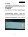
An SDK often comes in the form of a downloadable file that can be interfaced
with an Integrated Development Environment or IDE (See IDE Section for more
details). Within the IDE, the SDK can help by providing tools such as interface
creation, sample code, and device emulators to jump start the learning process
for a new platform and assist in a speedy development cycle. These SDK’s are
provided by the operating system’s owners such are Google or Apple to give
incentives to third party application programmers to develop on their mobile
platform [26].
In this section we picked out the three main areas that pertain to Project AUGI
the most. These three areas are: Interface Creation/Editing, Platform and Tools,
and Device Emulators and Simulators. Because our group is new to mobile
application development, initial requirements are that the setup of the appropriate
IDE, API, and SDK be simple and straightforward, creating trivial things like the
user interface be simple and almost done for us so there is more time to work on
core components and functionality, and all of our current machines be compatible
with the respective SDK due to budget limitations [26].
9
[GROUP 12 SENIOR DESIGN DOCUMENT SPRING 2013] April 29, 2013
3.1.1.1.Interface Creation/Editing
Interface creation within an application can be a very trivial yet time consuming
task. Many times developers find themselves spending too much time on code
pertaining to the user interface and not enough time on the core functionality of
the application. Thankfully; Google, Microsoft, and Apple have all included
interface creation tools that will assist and reduce the amount of time spend on
creating a usable graphical interface which in turn, will free up time spent on
developing the core functionality. The strengths and weaknesses of the three
competitors are described below.
3.1.1.1.1.
Android
Androids
Layout
Editor
is
Google’s answer to building an
android interface and underlying
functionality within an Android
application. Using this layout
editor, you have the ability to
visually create the graphical
interface which that you wish to
use. This layout editor is tightly
associated with the XML that it
generates within your code.
Many developers online agree
that Google’s layout editor seems
a bit crude, and they often found
themselves editing the generated
XML code themselves. Android’s
Layout Editor does have its
advantages though. Android’s
mechanism
for
configuring
referencing
outlets
for
UI
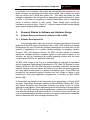
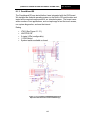
Figure3.1.1.1.1.1: Google's Layout Editor
Google Open Instruction Image
elements is agreed to be the
most intuitive of all the competitors. Lastly, the documentation for theming and
styles in Android is not as helpful as the others [27].
3.1.1.1.2.
iOS
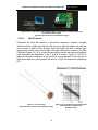
Apple has developed an interface building tool called, Interface Builder (See
Figure 3.1.1.1.2.1). Apple’s Interface builder is the most polished interface
creation tool of its competitors. Interface Builder makes manipulating and adding
components to your user interface simple. By taking advantage of drag and drop
features for almost every graphical situation, directly editing XML becomes
almost non-existent. Apple also has the advantage in the user interface
10
[GROUP 12 SENIOR DESIGN DOCUMENT SPRING 2013] April 29, 2013
development arena because of its support for only one screen resolution. This
means, unlike Android and Windows Phone that layouts do not have to be
specified in any specific way to allow them to conform to the standard [34].
Figure 3.1.1.1.2.1: iOS Layout Editor
Apple Open Instruction Image
3.1.1.1.3.
Windows Phone
Windows Phone 8 is a fairly new
operating system, so not many
people have tried and tested the
SDK environment yet.
The
Windows Phone SDK is basically
a subset of Microsoft’s rich UI for
web enabled content. Because
the Windows Phone SDK is so
similar to Microsoft’s Silverlight, it
is logical to understand Silverlight
is first before trying to understand
Windows Phone SDK. Silverlight
is used for running rich internet
applications and is very similar to
Adobe Flash. Silverlight is most
Figure 3.1.1.1.3.1: Windows Phone 8 Layout Editor
Microsoft Open Instruction Image
commonly used in web browsers
and can be enabled as an add-on similar to Flash. Silverlight is the driving force
11
[GROUP 12 SENIOR DESIGN DOCUMENT SPRING 2013] April 29, 2013
behind many of Microsoft’s web based development. Microsoft has provided the
community with downloadable UI templates for developers to use. The user
interface design tool Microsoft provides is called Microsoft Expression Blend.
This is a separate module sold by Microsoft itself. Expression Blend works
seamlessly with Visual Studio (Microsoft’s own official Integrated Development
Environment) which makes it easy to move objects back and forth without the
need for conversions [35].
3.1.1.1.4.
Winner
Overall, the Interface creation among the 3 platforms is very competitive; from
Android’s extremely versatile development environment, to IOS’s polished and
easy and straightforward Interface Builder, to Microsoft’s well-integrated
development ecosystem. The two interface creation mechanisms that seemed
the most complete were Apple’s IOS and Microsoft’s Windows Phone. Android
fell short when it came to usability and completeness, and when time is of the
essence that is a risk that must be considered.
3.1.1.2.
Platform and Tools
Development tools are a crucial in a speedy development process. This is an
area where these platforms begin to show their differences as far as SDK
features goes. This is also an area that Project AUGI is especially concerned
about due to our limited budget and the magnitude of the cost of a new computer
using a supported operating system. Platform describes the operating system
that developers are allowed to build the software on. Tools for an SDK include
Integrated Development Environments (IDE’s) that are platform dependent. An
Integrated Development Environment is a piece of software that offers a large set
of tools for programmers to assist in software development. An IDE normally
consists of a source code editor, build automation tools and a debugger. A
platform can also be replaced by a virtual machine which can run the operating
system with another operating system. Utilizing this virtual machine software can
solve the problem, but more time and money must be spent in buying new
licenses and configuring some virtual machine specific settings (Such as Hyper-V
for Windows Phone 8 which is required to run their device emulator).
3.1.1.2.1.
Android
Google has allowed software developers to choose between virtually any
desktop operating system of their choice which includes: Apple’s OS X,
Microsoft’s Windows, or Linux. This opens up a wide range of IDE’s to choose
from and allows our group to develop across different desktop platforms which
becomes a problem when a tight budget is involved. This is a positive for project
AUGI, because of this versatility no funds will have to be wasted on the
development portion of the project. Although the use of virtually any Java
12
[GROUP 12 SENIOR DESIGN DOCUMENT SPRING 2013] April 29, 2013
development IDE is possible, Eclipse seems to be the IDE of choice for one big
reason; Google’s SDK has only been fully integrated on Eclipse [26].
3.1.1.2.2.
iOS
Apple has made the decision to only allow developers to build IOS applications
on computers running their desktop operating system OSX, in other words, a
Macintosh. This restriction was crucial in making our decision in picking our
mobile platform. Due to this fact, a limited number of IDE’s are available for use.
XCode is arguably the only useable IDE for developers to use, and because of
this also limits options dramatically. There are other IDE’s available when
programming in Objective-C but XCode seems to be the fan favorite [34].
3.1.1.2.3.
Windows Phone
Microsoft’s Windows Phone 8 SDK includes Visual Studio 2012 Express as its
main IDE. Visual Studio can only be installed and run on a machine running
Windows operating system on it. Mac OSX and Linux are not yet supported.
Visual Studio supports development in Windows Phone’s main programming
language which is C#. There are other development environments to choose
from when programming in C# such as Monodevelop. Monodevelop is supported
across Windows, OSX, and Linux. Although there are some other alternatives to
Visual Studio, the programming community is in agreement that Visual Studio
Express is the most convenient one [35].
3.1.1.2.4.
Winner
The winner of this round will go to Google’s Android because of its versatility and
many development options. Because of Android’s SDK ability to develop on
almost any platform, the need for virtual machines and compatibility issues no
longer becomes a problem and everything in the end will work as close to
seamlessly as possible. Microsoft and Apple have a road ahead of making their
SDK’s runnable on other machines besides their own, and sadly because of that
fact the world may never see them rolled out for other operating systems.
3.1.1.3.
Device Emulators and Simulators
Device Emulators have become a necessity in the mobile application
development realm. A device emulator is supposed to mimic the user-device
interaction without working on the actual physical device. If a device has 1GB or
RAM that runs on a 1.3 GHz Snapdragon S3 processor, the device emulator
should present the same type of performance that is expected of the physical
device. Software nowadays is not developed and run on the same machine like it
used to be. Due to this fact, device emulators were created to speed up testing
and debugging time. Time and money is a big road block and the ability to run a
virtual device’s screen on your desktop and test a virtual device instead of a
physical one is crucial.
13
[GROUP 12 SENIOR DESIGN DOCUMENT SPRING 2013] April 29, 2013
Devices also come in a large amount of configurations and hardware options. For
example, a mobile operating system such as Android has countless devices
manufactured by Samsung, Motorola, HTC, etc. Each of these devices features
different screen resolutions, processors, cameras, and peripheral connectors, all
of which has to be taken into account when the development of an application is
considered. Device Emulators allow someone to test across all of these with the
click of a button. The sections below will describe the device emulators each
platform’s SDK features.
3.1.1.3.1.
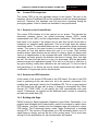
Android
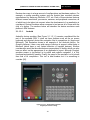
Android’s device emulator (See Figure 3.1.1.3.1.1) remains unpolished like the
rest of the available SDK. It does not have features such as the on screen
keyboard and physical device-like navigation like its competitors do (Apple and
Microsoft). The illustration shown is an example of the Androids device. On
Google’s defense, it has a very wide range of devices to support unlike Apple or
Microsoft (which have a very limited selection of handset devices). Another
consideration would be the manufacturers personalized UI builds, which can also
have an effect on the appearance of an application’s layout. Although Google’s
emulator seems to lag behind in its polish and realistic navigation, it is fully
functional and perfectly useable. Finally, the speed of the emulator is a bit slower
than that of its competitors. This isn’t a deal breaker but it is something to
consider [26].
Figure 3.1.1.3.1.1: Android Device Emulator
Google Open Instruction Image
14
[GROUP 12 SENIOR DESIGN DOCUMENT SPRING 2013] April 29, 2013
3.1.1.3.2.
iOS
Apple’s iOS continues to be the
most polished SDK around offering
the fastest and most realistic virtual
device
interface
(See
Figure
3.1.1.3.2.1). Apple’s simulator also
features a completely functional
keyboard that behaves exactly like
the one on their physical phones.
Navigation is also realistic in the
sense that it behaves just like its
physical
look-alike.
Swiping
gestures on the physical devices is
mimicked by clicking and dragging
and applications are opened by
clicking. Another impressive feature
Figure 3.1.1.3.2.1: Apple Device Emulator
Apple Open Instruction Image
about iOS’s device emulator is the
speed. It is smooth and on par with its physical devices. The only downside to
the iOS simulator is that fact that it is a simulator itself. This can be a downside
because when testing the performance of an application, you won’t get a real
world estimate of how well the application will perform on an actual device. This
is also noticeable when keeping track of memory consumption and available disk
space. Upon viewing the system specs of a simulated iPhone within the
simulator, the development computer’s specs will appear rather than the specs of
the phone in question [34].
3.1.1.3.3.
Windows Phone
Windows Phone’s SDK package is
beginning to gain its reputation as
one of
the more polished
development kits available. With
Windows new roll out of Windows
Phone 8, many changes were
made to both the operating system
itself and its software development
kit. With these new added SDK
features, Microsoft is now upping
the system requirements of the
development PC you can work on
now. With the new Windows Phone
8 SDK comes the addition of
Microsoft’s very own Hyper-V
requirement to run the Windows
Figure 3.1.1.3.3.1: Windows Phone 8 Device Emulator
Microsoft Open Instruction Image
15
[GROUP 12 SENIOR DESIGN DOCUMENT SPRING 2013] April 29, 2013
Phone 8 emulator (See Figure 3.1.1.3.3.1).
Since many developers have the own preference of operating system and prefer
not change when switching to a new development platform (because of platform
limitations i.e. Apple and Microsoft) they often find themselves running on virtual
machines within their preferred operating system to get the job done. To run the
Windows Phone Emulator within a virtual environment, Second Level Address
Translation (SLAT) is needed and this, in turn, needs Hyper-V on the server.
Hyper-V has become somewhat of a hurdle for many developers on the web now
having to revamp their systems after the new change [35].
Once the Emulator is setup and running, performance is fast and the interface is
sleek. Navigation within the UI is just as it would be on the physical devices and it
is smooth and accurate. This fact puts it in direct comparison with the iOS
simulator by Apple except for the fact that Microsoft took it a step further and
added the extra “emulator” functionality to give it the correctly emulated
processor speed, memory support, and storage availability. Options like
changing color accents and adding email and administrative accounts are also
available in the emulated window.
3.1.1.3.4.
Winner
The winner of this Software Development Kit Emulator round will have to be
Windows Phone 8’s Emulator. With its highly polished and true-to-life emulation,
Microsoft has done their homework when it comes to making an emulator that
developers want to work on. Although there is the added hassle of setting up the
virtual machine to Hyper-V’s liking, for this project we will not be using any
servers to simulate the Windows environment requirement. iOS was in a close
second, but due to our application being very hardware intensive, a simulated
environment that utilizes hardware far beyond the physical devices just won’t cut
it. Android’s emulator is great if a developer is looking for purely functionality, but
just cannot compete with Microsoft’s polish and equaled functionality.
3.1.1.4.
Programming Language Options
Another aspect when considering which OS platform to choose as the foundation
for our project is considering which programming languages are usable for each.
For Apple's iOS platform this means using Objective-C. Objective-C is an object
oriented programming version of the C programming language. It adds object
oriented syntax features to the existing C base, which means it is fully backwards
compatible with regular C code. Objective-C is the only programming language
allowed for application development on Apple devices [1].
16
[GROUP 12 SENIOR DESIGN DOCUMENT SPRING 2013] April 29, 2013
3.1.1.4.1.
Android
For Google's Android platform, the programming language that is used for
application development is Java through the Android Software Development Kit
(SDK). The most popular IDE for application development is Eclipse. Eclipse is
a widely used IDE, that is highly flexible and extensible, so that it can be used for
coding in a wide variety of languages [27].
3.1.1.4.2.
iOS
Apple offers up Objective-C through its Xcode integrated development
environment (IDE). Xcode is used to develop all iOS applications. This IDE
contains all the necessary pieces that are needed to develop applications for
Apple devices, including an integrated Interface builder for graphical user
interface construction (GUI), and developer documentation for building
applications [34].
3.1.1.4.3.
Windows Phone
Application development for Windows Phone 8 is done through the Windows
Phone Developer Tools, which can be integrated into the Visual Studios IDE. It
supports native C and C++ libraries, and uses a shared runtime known as the
Common Language Runtime. This allows easy porting of software between
Windows programs and Windows Phone 8 [35].
3.1.1.4.4.
Winner
For this project, the criteria for which of the three options listed above best suits
the projects needs, are familiarity with the programming language, the openness
of the development platform and its accessibility to custom hardware that we can
build with.
Since Objective-C is only available through Apple's Xcode, which is further
restricted to operating on Apple hardware, it is unsuitable to the needs of this
project. Windows Phone 8 also falls through due to these same limitations. The
openness of the Android platform however, and its use of Java, which is a very
widely used programming language meets the needs of the project perfectly.
The design team can build its custom hardware, and install the Android OS onto
it. It can further develop the needed navigation aid application using the highly
familiar and common Java programming language. This further supports the
choice of the Android OS as the software foundation for this project.
17
[GROUP 12 SENIOR DESIGN DOCUMENT SPRING 2013] April 29, 2013
3.1.2. Multiple Platform Cross Compatibility and Porting Requirements
In this day and age where there are so many new mobile platforms and operating
systems arising, platform cross compatibility and porting requirements are
becoming more and more relevant. This is because software development
companies now have to convert or port their application from its primary
development platform to a new platform to stay relevant. Problems can arise
when complex programs are rewritten on another platform due to different API
calls and system references. Along with API differences comes the hardware
variations associated with respective devices running their mobile platforms. With
different hardware also come more compatibility issues. For these reasons,
porting an application has become less trivial than the past.
There are many outsourcing availabilities out there in the wild providing platform
to platform conversions, one of the most popular being a firm called Two
Toasters.
3.1.2.1.
Android
Many Android developers nowadays are seeing how beneficial developing an
application for one of the most popular mobile platforms in the world can be, and
would like to expand their audience.
Google has done a lot of the work for Android developers and created a porting
tool to assist in the porting from Android to iOS devices (this includes iPhones,
iPod Touches, and iPads). The program is called J2OBJC and is basically a Java
to Objective-C translator. J2OBJC achieves this by converting Java classes to
Objective-C classes by directly using the iOS Foundation Framework. GUI
related elements are not supported, but the core functionality Java source code
is. J2OBJC supports the complete Java 6 language and most of its runtime
features that are required by client-side application developers and include:
exceptions, inner and anonymous classes, generic types, threads and reflection.
Also, the translation of JUnit test and execution is built in. Also, many IDE’s such
as Xcode and Make can take advantage of J2OBJC.
At the moment there is not one-to-one port tool available for Android to Windows
Phone 8. Microsoft has released some tools to assist in the API translations
between the two platforms. Some of these tools include the formation of an
Android to Windows Phone API mapping tool and a service called “App Guy” that
scours the internet for porting questions regarding Windows Phone 8 and any
porting issues developers may be having. The bottom line is that the application
will have to be rewritten in a Windows Phone 8 form factor.
18
[GROUP 12 SENIOR DESIGN DOCUMENT SPRING 2013] April 29, 2013
3.1.2.2.
iOS
iOS to Android porting is not as simple as Android to iOS, and there is no porting
automation available yet. In fact, Objective-C cannot even be re-compiled into
Java for Android. Besides that demotivating fact, when trying to rewrite an iOS
application for Android, the immense size of device configurations becomes a
problem. Android devices come in different sizes, pixel densities, processor
speeds, Android versions, etc. In the event that an iOS application uses basic C
code then there is a possibility that the code can be reused in Android.
For porting iOS to Windows Phone 8, a code rewrite is also necessary as there is
no known porting option. Microsoft has provided the same type of documentation
that it’s provided for porting Android to Windows Phone. This document is called
the iPhone API mapping tool and makes the migration process much less time
consuming [34].
3.1.2.3.
Windows Phone
Windows Phone 8 is still a new operating system and chances are an application
won’t initially be developed on it before other platforms. There seems to be no
trivial away for anyone to port a Windows Phone Application to any other
platform at the moment. Because it is a Windows Phone, there was a lot of
discussion regarding porting an application to a Windows desktop environment,
but that without any substantial porting tools also. Also, the fact that Microsoft is
less interested in making developers move their applications to another platform
until it starts to gain some more momentum in the mobile handset realm.
3.1.2.4.
Conclusion
To conclude, there is a clear advantage among one of the platforms within this
list, Android. Google has developed their own J2OBJC porting application that is
the only true porting utility out there on the market to port to iOS. Microsoft also
supplies Android to Windows Phone API translations for easy look ups and code
rewrites. It is general consensus though, that porting a phones graphical user
interface is neither supported nor is it a good idea for developers to do. Taking
advantage of a platform’s strengths as far as its user interface is a big deal, and if
it means code re-writes, so be it.
3.1.3. Hardware/OS Platform Flexibility
When picking a new mobile platform to start developing hard for, one question
that hardware developers ask themselves is: “How easy will it be to integrate new
hardware into the operating system?” There are some key differentiators when it
comes to developing hardware for the big three players in the mobile handset
19
[GROUP 12 SENIOR DESIGN DOCUMENT SPRING 2013] April 29, 2013
game. There are also certifications involved when it comes to being eligible to
receive their support when it comes to API’s and integration. This fact can slow
down the development process because of the time it takes a big company like
Apple to approve a project and give you access to their integration libraries [29].
Project AUGI will need to communicate to a handset device via some sort of
input port. Input methods change because to the input support each device
carries. For example, the standard protocol for a USB port will differ from the
protocol on iPhones Lightning connector. The design decision will ultimately be
chosen and their reasons explained further in the documentation. The sections
below will explain the process it takes, for each mobile platform, to develop a
piece of hardware. Mobile platform’s will often release hardware development
kits to jump start and entice developers to start building hardware for their
platforms so there is a richer and more option filled experience for the end-user.
Companies such as Apple and Google have released their own hardware
development kits and it has proven to be successful in luring customers to their
platform because of a more accessory rich environment.
3.1.3.1.
Android
Google’s Android, unlike Apple, does not need a certification to develop
hardware. There is no approval process, and in turn, no wait time to begin
development. Google supplies an Accessory Development Kit or ADK on their
website for anyone looking to get into developing hardware for their platform. The
Accessory Development Kit is for anyone and is a reference implementation
starting point for building accessories for Android. An accessory includes speaker
docks, credit card scanners, or anything else that can interface with a handset
running android. These accessories use AOA or Android open accessory
protocol in order to communicate between a handset and the piece of hardware;
this includes wired connections such as USB or wireless connections such as
Bluetooth [29].
The latest version of Android’s ADK is based on the Arduino open-source
electronics prototyping platform with some modifications that help it integrate with
Android devices. With the purchase of an Android Development Kit comes a
hack-able Arduino box that contains every sensor imaginable. It can be used to
find the right combination of hardware for a developer’s specific purpose to then
be built and put into production.
There is currently no certification program for new Android hardware, which
means that customers can’t expect anything from quality of their hardware. It also
means that dependable manufacturers are at a disadvantage because of the
consumer confusion when shopping for a new accessory.
20
[GROUP 12 SENIOR DESIGN DOCUMENT SPRING 2013] April 29, 2013
3.1.3.2.
iOS
Apple has always maintained a closed ecosystem, regulating all the
device accessories, applications and even the devices themselves. Building a
piece of iPhone hardware is no different. The first step in the hardware
development process for an Apple iPhone product is to become a member of
Apple’s MFi program. This program will give a developer access to: the hardware
components and documentation, allow you to use the official MFi certified logos,
and allow you access to Apple’s technical support engineers.
This is a lengthy process requiring things like: a credit review, the write up of an
enrollment form, and even Apple’s analysis of the developer to determine if Apple
thinks Apple hardware development is right for them. Upon becoming an official
hardware developer, Apple requires you only use the components that they
approve and exclusively buy it through them. Being a company is also another
problem area. Apple only accepts certified companies before they even consider
looking over any approval papers. There are no fees when applying for the MFi
program, but Apple requires you to pass a standard series of third-party tests to
demonstrate that the piece of hardware won't interfere with the iOS hardware
built in [34].
Among all of these requirements and restrictions, it will be close to impossible for
Project AUGI to develop and Apple related hardware in a timely manner.
Submitting the application for MFi seems difficult enough, on top of earning the
privilege to become hardware for Apple seems near impossible.
3.1.3.3.
Windows Phone
Windows Phone 8 is still in early development at this point and does not have
any official development kits at the moment. In order to develop any hardware for
Windows Phone 8 you must be a Microsoft hardware partner right now. These
companies include Nokia, HTC, Samsung, etc. The reason for this is probably so
the early adopters get a good end-user experience because they are using
hardware made by reputable companies. As the ecosystem and the platform as a
whole get stronger we may see Microsoft release a hardware development kit.
3.2.
Hardware Resources Research
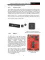
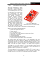
3.2.1. Reference Board Hardware Summary
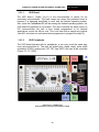
The hardware for our project revolves around the PandaBoard ES. The
PandaBoard ES is the heart and brains of this project (See Figure 3.2.1.1). It was
the platform which the operating system, the latest version of Android, ran on.
This board was mounted on the Panda expansion board which has a 7.0 inch
LCD screen. A resolution of (800 by 480 pixels); with five point capacitive touch,
21
[GROUP 12 SENIOR DESIGN DOCUMENT SPRING 2013] April 29, 2013
and five user keys/buttons. There was also a three-axis digital accelerometer and
three axis digital compass which we did not use for our project.
Instead our sensors were from a custom made PCB board that is attached via
the USB port into the Panda Board ES. The 7 inch LCD screen, Pandaboard ES,
and Panda expansion board are mounted on a plastic frame to neatly and
aesthetically hold everything together. The Pandaboard ES does not have
sensors, like a barometer, accelerometer or gyroscope. Some of these sensors,
like an on board accelerometer are featured on the expansion board, however,
instead of using the prebuilt sensors on the expansion board, a custom design
PCB board read in all of these sensors.
This custom PCB board has the IOIO circuitry within, which acts as a USB host
and interprets commands from our Android app programmed in the Panda
Board. The custom PCB board also includes other sensors such as:
accelerometer, gyroscope, barometer, GPS, GPS antenna, ambient light/photo
sensor, temperature and sensor. Two 2200mAh polymer lithium ion batteries
were used to power all the devices, alternating while one was being recharged.
Our custom made PCB included circuitry to regulate and a separate charger to
recharge the battery packs.
Figure 3.2.1.1: Reference Board Hardware Description Image
3.2.1.1.
Primary Microcontroller
The microcontroller is the most essential part of this project. Even before
deciding which board to use, we first created a list of requirements our project
needs. Unlike typical microcontrollers, which often have under 100 KB of RAM,
we needed a system on chip that had a processor powerful enough to run an
operating system like Window or Linux, preferably any ARM Cortex-A8 or later.
In our case it is the Android Operating system.
We also wanted our microcontroller to be as open source as possible. At first we
looked into the Raspberry Pi. When we compared it with the features of the
Beagle Board or Panda Board, it seemed to lack many of the features we
22
[GROUP 12 SENIOR DESIGN DOCUMENT SPRING 2013] April 29, 2013
needed. Therefore the Raspberry Pi was out of the picture. Next we looked into
the Beagle Board. The Beagle board was very open source and could run the
Android OS. It had sample codes and step by step tutorials over the internet.
We then looked into the Panda board. The big difference between the Beagle
board and the Panda board is that the Panda Board had most of the hardware a
smart phone would have, like audio jack, camera expansion and SD slot. Our
project is to create an augmented reality via an android app. If our development
board has all the features a smart phone has, it would be possible to use the
software not only on our device but on any android devices. The Panda board is
also very open source so at the end we decided that this microcontroller was our
best bet. There are two kinds of Panda board, The Panda Board and The Panda
Board ES. The ES version has the OMAP4460 (1.2 Ghz) vs the regular version
which has OMAP4430 (1.0 Ghz). Not only was the ES faster, but it also supports
TiWi-BLE, has a sysboot control to control the boot order, support AFML/R, and
a hand full of other features. Thus we picked the Panda board ES.
3.2.1.2.
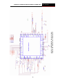
Pandaboard ES
The Pandaboard ES (See Figure 3.2.1.2.1 Figure 3.2.1.2.2) is based on a
system on chip(SoC), the OMAP4460 by Texas Instruments. It is designed to be
low-power consumption, cost effective single-board computer for development.
The OMAP4460 is a duel-core A9 CPU with a 384 MHz GPU, and has 1 GiB of
DDR2 SDRAM (See Figure 3.2.1). The board is completely open sourced and is
a community supported development platform.
The PandaBoard ES can run an array of operating systems, such as: Windows
CE, WinMobile, Symbian OS, Linux, which includes any of the Android OS, and
Palm OS. The Pandabord ES has additional expandability via onboard
connectors throughout the board (See Figure 3.2.7). It can output 1080p from
either its HDMI or DVI ports. It also comes with Wi-Fi(See Figure 3.2.8),
Bluetooth, LAN port (See Figure 3.2.8) and much more [1].
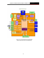
Listed below are the major components used on the PandaBoard.
OMAP4430 Processor (See Figures 3.2.2, 3.2.3, 3.2.4)
TWL6030 (Phoenix) Power Management Companion Device (See Figure
3.2.5)
TWL6040 (Phoenix) Audio Companion Device (See Figure 3.2.6)
POP Mobile LPDDR2 SDRAM Memory
HDMI Connector (Type A) – for OMAP4430 HDMI Transmitter output (See
Figure 3.2.11)
HDMI Connector (Type A) – for DVI-D output sourced via OMAP4 parallel
display output (See Figure 3.2.11)
Audio Input & Output Connectors (3.5mm)
SD/SDIO/MMC Media Card Cage (See Figure 3.2.10)
LS Research Module – 802.11b/g/n, Bluetooth, FM
23
[GROUP 12 SENIOR DESIGN DOCUMENT SPRING 2013] April 29, 2013
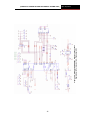
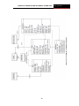
Figure 3.2.1.2.1: Block Diagram for Panda Board ES
Reprinted with Permission from Panda Board [1]
24
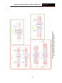
[GROUP 12 SENIOR DESIGN DOCUMENT SPRING 2013] April 29, 2013
Figure 3.2.1.2.2: Top View of the Panda Board ES
Reprinted with Permission from Panda Board [1]
3.2.1.3.
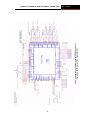
Processor OMAP4460
The Pandaboard ES is a platform for the OMAP4460, which has many powerful
multimedia features, while also staying low cost. The OMAP4460 is developed by
Texas Instruments and is a category of proprietary, system on chip, (SoC) for
portable and mobile multimedia applications. The OMAP4460 is a duel-core CPU
with a 384 MHz GPU. It also has 1 GiB of DDR2 SDRAM(double data rate
synchronous dynamic random-access memory) The chip uses an Advanced
RISC Machine (ARM) architecture and uses 45-nm technology [1].
This type of CPU design (ARM) is the most widely used in portable devices such
as the Iphone and other smart phones. The OMAP4460 is designed to provide
best in class video, graphics, and image processing for various applications. The
PandaBoard ES has an intergrated SGX540 graphics processor and can output
1080p through HDMI and DVI output ports (See Figure 3.2.11). This graphics
processor will also support OpenGL ES, OpenVG, and other graphic base
25
[GROUP 12 SENIOR DESIGN DOCUMENT SPRING 2013] April 29, 2013
programs. Usually an internal clock in the battery allows devices to keep time.
The PandaBoard ES, however, does not have a battery to save the time when
the power is disconnected. Instead there is a software clock that can set the
clock time during the bootup as the PandaBoard ES starts up. The low power
design of this board will prove ideal when the design team attaches a battery to
make the platform mobile(See Figure 3.2.12) [1].
3.2.1.4.
Operating Temperature of OMAP4460
We are using the OMAP4460 (1.2 Ghz) processor in our system. For reliability
and operability concerns, the absolute maximum junction temperature of the
OMAP4460 has to be below 125ºC and the maximum average junction
temperature has to be below 110ºC.
Depending on the thermal mechanical design (Smartphone, Tablet, Personal
Navigation Device, etc), the system thermal management software, and worst
case thermal applications; the junction temperature might be exposed to higher
values than those specified above. Therefore, it is recommended to perform
thermal simulations at the device level (Smartphone, Tablet, Personal Navigation
Device, etc) with the measured power of the worst case UC of the device.
The OMAP level thermal policy relies on a PCB sensor. Therefore, it is
recommended to have such sensors located on the PCB. In addition, it is
recommended to avoid having another significant thermal source near the
OMAP4460 by TI. So to be able to run the designed system efficiently at the
desired thermal level, we must follow these testing parameters
.
The risks of not managing this junction temperature are hazardous heating,
power supply clamping, reliability issues, and malfunction [1].
26
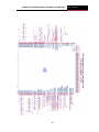
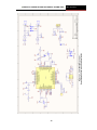
Figure 3.2.1: OMAP4460 Logic Block Diagram
Reprinted with Permission from Ti [22]
[GROUP 12 SENIOR DESIGN DOCUMENT SPRING 2013] April 29, 2013
27
Figure 3.2.2: OMAP4460 Symbol A
Reprinted with Permission from Pandaboard [1]
[GROUP 12 SENIOR DESIGN DOCUMENT SPRING 2013] April 29, 2013
28
Figure 3.2.3: OMAP4460 Symbol B
Reprinted with Permission from Pandaboard [1]
[GROUP 12 SENIOR DESIGN DOCUMENT SPRING 2013] April 29, 2013
29
Figure 3.2.4: OMAP4460 Symbol C
Reprinted with Permission from Pandaboard [1]
[GROUP 12 SENIOR DESIGN DOCUMENT SPRING 2013] April 29, 2013
30
Figure 3.2.5: TWL6030 Power Management Companion Device
Reprinted with Permission from Pandaboard [1]
[GROUP 12 SENIOR DESIGN DOCUMENT SPRING 2013] April 29, 2013
31
Figure 3.2.6: TWL6040 Audio Companion Device
Reprinted with Permission from Pandaboard [1]
[GROUP 12 SENIOR DESIGN DOCUMENT SPRING 2013] April 29, 2013
32
Figure 3.2.7: Pandaboard ES Video and Camera Connections
Reprinted with Permission from Pandaboard [1]
[GROUP 12 SENIOR DESIGN DOCUMENT SPRING 2013] April 29, 2013
33
Figure 3.2.8: Pandaboard ES Wifi Connections
Reprinted with Permission from Pandaboard [1]
[GROUP 12 SENIOR DESIGN DOCUMENT SPRING 2013] April 29, 2013
34
Figure 3.2.9: Pandaboard ES USB + Ethernet Connections
Reprinted with Permission from Pandaboard [1]
[GROUP 12 SENIOR DESIGN DOCUMENT SPRING 2013] April 29, 2013
35
[GROUP 12 SENIOR DESIGN DOCUMENT SPRING 2013] April 29, 2013
Figure 3.2.10: SSMMC and USB PHY
Reprinted with Permission from Pandaboard [1]
36
[GROUP 12 SENIOR DESIGN DOCUMENT SPRING 2013] April 29, 2013
Figure 3.2.11: Pandaboard ES Video output
Reprinted with Permission from Pandaboard [1]
37
Figure 3.2.12: Pandaboard Power Circuits
Reprinted with Permission from Pandaboard [1]
[GROUP 12 SENIOR DESIGN DOCUMENT SPRING 2013] April 29, 2013
38
[GROUP 12 SENIOR DESIGN DOCUMENT SPRING 2013] April 29, 2013
3.2.1.5.
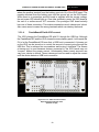
Panda Expansion Board
The Pandaboard ES expansion board, designed and produced by ChipSee, is a
board that allows the Panda board ES to plug right into it via several pin
connecters (See Figure 3.2.1.5.3). It adds many features that aid developers and
speed up the development process. This includes either a four wire resistive
touch or capacitive touch screen, a 7 inch LCD screen (See Figure 3.2.1.5.5),
three-axis digital accelerometer (See Figure 3.2.1.5.6), three-axis digital compass
(See Figure 3.2.1.5.4) and five user keys/buttons.
The capacitive touch is used in this project. It also comes mounted on a plastic
board that holds the LCD screen and the circuitry together. There is also a 3G
module that supports SIM5320 (See Figure 3.2.1.5.2) which is sold separately.
This would support data and voice which include WCDMA, and GPS. We will not
be using the wireless capabilities from this board, nor will we use the three-axis
digital accelerometer or three-axis digital compass. The main purpose for the
Panda Expansion board is to use the 7 inch LCD screen with its capacitive touch
and the plastic mount that holds the expansion circuitry. We will also use the five
user keys/buttons.
Figure 3.2.1.5.1: Top and Bottom of Panda Board ES
Reprinted with Permission from Parallax [2]
39
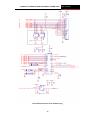
Figure 3.2.1.5.2: SIM 5320 Schematic
Reprinted with Permission from Parallax [2]
[GROUP 12 SENIOR DESIGN DOCUMENT SPRING 2013] April 29, 2013
40
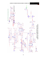
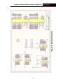
Figure 3.2.1.5.3: Expansion Board Connectors
Reprinted with Permission from Parallax [2]
[GROUP 12 SENIOR DESIGN DOCUMENT SPRING 2013] April 29, 2013
41
Figure 4.2.1.5.4: Expansion Board Digital Compass
Reprinted with Permission from Parallax [2]
[GROUP 12 SENIOR DESIGN DOCUMENT SPRING 2013] April 29, 2013
42
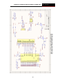
Figure 3.2.1.5.5: Expansion Board LCD Screen Connectors
Reprinted with Permission from Parallax [2]
[GROUP 12 SENIOR DESIGN DOCUMENT SPRING 2013] April 29, 2013
43
Figure 3.2.1.5.6: Expansion Board DS90C385
Reprinted with Permission from Parallax [2]
[GROUP 12 SENIOR DESIGN DOCUMENT SPRING 2013] April 29, 2013
44
[GROUP 12 SENIOR DESIGN DOCUMENT SPRING 2013] April 29, 2013
3.2.1.6.
Seven Inch LCD
The 7 inch LCD screen comes with the purchase of the Panda expansion board
designed and produced by ChipSee (See Figure 3.2.1.6.1). When buying the
Panda expansion board we had the option to choose between the capacitive
touch and the resistive touch screen. We first looked into the resistive touch
screen. It was made from a normal glass panel that is coated with three layers.
Two of these layers are conductive and resistive and the third layer is a hard
cover that covers the hold setup. For resistive touch screens, current flows
through these layers when the system is running. With a touch of a finger a
change in the electrical field occurs. This is a single touch system. The system
then calculates the coordinates of the point of contact and the touch screen
drivers passes it to the rest of the system.
The capacitive touch screen on the other hand, is capable of multi touch. The
glass panel is made up of a material that can store an electrical charge. The
human finger also stores an electrical charge. When a finger touches a
capacitive touch screen, some of the charge transfers from the screen to the
finger. The oscillator circuit within the circuitry of the screen detects the change in
electrical charge and the exact location of where the touch occurred. This data is
then transfer to the touch screen driver for processing.
After we understand how both touch screens functioned, we needed to see which
screen fit our project needs. The first and most apparent feature was the multi
touch on the capacitive touch. Because our application may use multi touch we
wanted our LCD to be able to grow with the software needs. Next is the fast
response of the capacitive. Like most smart phones, the touch needs to be very
responsive and fast pace. The capacitive touch was the clear winner in this
department as well. It also had a nice glossy finish, and was much more visible
over sunlight. And because this device is intended for outdoor use, this was a
major deciding factor. Overall the capacitive touch came out to be the better
screen for our project. Thus we picked the capacitive for this project.
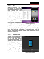
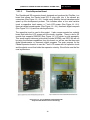
Figure 3.2.1.6.1: Expansion Board LCD in Action
45
[GROUP 12 SENIOR DESIGN DOCUMENT SPRING 2013] April 29, 2013
Below in Figure 3.2.1.6.2 is a list of pros and cons for both resistive touch and
capacitive touch screens:
Resistive Touch
Capacitive Touch
PROS of Resistive Touch:
It’s relatively cheaper compared with
capacitive touch.
Can function with any pointing device,
pen, nail, etc.
Can operate at any level of humidity
More accurate than capacitive touch
PROS of Capacitive Touch:
Supports Multi touch
Visible under sunlight
Glossy look and feel
More sensitive to finger
easier to use
More responsive
CONS of Resistive Touch:
Multi touch is not available
Reflective layer cause poor visibility in
sunlight
More vulnerable to scratches
More vulnerable to unwanted pointing
device/dust
CONS of Capacitive Touch:
5% humidity to achieve capacitive
effect
More expensive than resistive touch
screen
Does not work with inanimate
objects
touch,
Figure 3.2.1.6.2: Touch Screen Type Comparison
3.2.2. Output Screen Options
The design team has given careful consideration to the output screen options for
this project. Initially the idea of building a tablet with a transparent LCD screen
was considered (See Figure 2.1.1). This had a certain level of “coolness” going
for it, and would provide for a more seamless user experience, since the user
would have the feeling of directly interacting with the world they are using their
tablet for to augment.
The biggest problem with transparent LCD screens however is that transparent
LCD screens are mostly in a prototype stage, and thus are hard to come by. At
the time of this writing there were none that the design team was able to
purchase.
There are a few engineering issues that the team would have to overcome as
well with the use of a transparent LCD screen. The first is that LCD pixels do not
generate their own light. LCD screens normally rely upon a florescent lamp to
provide the light needed to see the image. A transparent LCD screen however
has no such lamp, and thus relies entirely upon ambient light to operate. This
means that in low light conditions, or at night, it would be difficult or impossible to
see anything on the transparent screen.
One possible solution to this problem that was derived by the engineering team is
to use a clear piece of glass with white LED’s arraigned along the outer edge of
46
[GROUP 12 SENIOR DESIGN DOCUMENT SPRING 2013] April 29, 2013
the glass to shine light into its edges. The glass should distribute the light along
the glass panel, and provide the needed illumination that the transparent LCD
needs, while still remaining transparent. However, until a supply of transparent
LCD panels is made available for purchase, it is not possible to pursue this path.
One other solution to the transparent LCD is to use a transparent OLED screen.
OLED pixels generate their own light, and thus don’t rely on ambient light to
operate. Although there are many demonstration exams out there, there are no
products available for purchase at the time of writing. If a product should
become available during the Spring 2013 Semester, the design team will
consider its integration to the tablet.
The next alternative considered is a more conservative approach, which involves
combining the tablets onboard camera, to feed a video stream to the tablets
regular LCD screen, in an attempt to replicate what the user would have seen
had the screen been transparent. This approach has the benefits of being simple
to implement from a hardware perspective and is the approach the design team
has chosen to adopt for the time being.
The final visual output option is to connect a pair of goggles that contain integrate
screens, capable of displaying to the users eyes, what they normally would have
seen on the tablet screen. This option has the benefit of freeing the users hands
when viewing the navigation application, and they also would grow tired of
holding the tablet up while navigating. However an alternative method for
controlling the tablet would need to be devised, since the user no longer has a
touch screen to manipulate the tablet.
For soldiers in the field, this is by far the best option. Soldiers often have very
heavy loads to carry as it is, and their hands are already busy handling their
weapons and equipment. By using the goggles, they can be integrated into the
ballistic glasses that soldiers already wear on the battlefield. With this key target
audience in mind, the design team will first focus on building the tablet with a
normal LCD screen, and if there is sufficient time and resources, attempt to add
the goggles feature via the video out port of the panda board.
3.3.
Custom Expansion Board
3.3.1. Secondary Microcontroller
The PandaBoard ES, our primary microcontroller, runs the augmented reality
application, while a second microcontroller processes all the data from our
sensors. This secondary microcontroller will then send the data via USB to the
PandaBoard ES. This way it will free up the PandaBoard ES and let it focus on
the application. There are many different microcontrollers on the market today
and finding the best one to fit our project was not easy.
47
[GROUP 12 SENIOR DESIGN DOCUMENT SPRING 2013] April 29, 2013
3.3.1.1.
IOIO Board
The IOIO board ( Called “yo-yo”) is the microcontroller of choice for our
secondary microcontroller. The main reason we chose this particular board is
because it is designed specifically to work with the Android operating system.
Also, since the PandaBoard ES will be running the Android operating system, the
IOIO board fits perfectly for our project. The chip is actually the same used in a
PIC microcontroller but with a boot loader programmed to let Android
applications control the 48 pin outs. This is all done with a simple and intuitive
Java API, and does not need an external programmer to program the chip[15].
3.3.1.2.
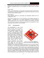
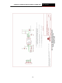
IOIO Peripherals
The IOIO board interacts with its peripherals, or pin outs, much the same way
most microcontrollers do. The pins are digital input, digital output, pulse width
modulation (PWN), analog input, I2C, SPI, and UART, and can all be controlled
(Figure 3.3.1.2.1) [20].
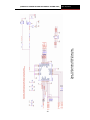
Figure 3.3.1.2.1: IOIO Pinout
Reprinted with permission from Sparkfun.com[3]
48
[GROUP 12 SENIOR DESIGN DOCUMENT SPRING 2013] April 29, 2013
1
USB Connector
The female connector that connects to the
PandaBoard ES
2
Ground Pin
The ground connection, power supply’s negative
terminal
3
Vin
The power supply’s positive terminal (5-15v)
4
5V Pin
5v output after the power supply is regulated
5
3.3 Pin
3.3 output after the power supply is regulated
6
I/O Pins
48 Pins, some are General purpose, some have
special function
7
Power LED
LED that light up when there is power
8
Stat LED
Lights up when under application control
9
MCLR Pin
Used to reprogram the boot loader firmware
10
CHG
Charge current trimmer, used to adjust how much
current is supplied into the USB port and into the
device
Figure 3.3.1.2.2: IOIO Pinout Description
The input and output pins are labeled to more easily identify which port has what
functions. Pins that have a square around them mean that they can be used as
3.3V analog input pins. Those with circles mean that they are 5V tolerant and can
be used as 5V logic output using an open-drain mode. You would also need a
pull-up resistor for this function. Next to the port with the “P” mark, means they
can be use as a peripheral input and output. These include pulse width
modulation, UART, and SPI. These “p” marked pins are especially important for
our project as they are what the sensors will be communicating through. The pins
marked with “Pi” can be used as a peripheral input but not output. And lastly the
pins marked with “DAx” and “CLx” are used for two wire interface (See Figure
3.3.1.4.1) [15].
3.3.1.3.
IOIO Power Supply
In order to power the IOIO board we need a DC voltage ranging from 5V to 15V.
A switching regulator steps the Vin to 5V with a limiting current of 1.5A. This is
49
[GROUP 12 SENIOR DESIGN DOCUMENT SPRING 2013] April 29, 2013
where the positive terminal from the battery goes into Vin of the IOIO board. The
negative terminal from the battery goes into the ground pin on the IOIO board.
When there is a connection and the board is supplied with the correct voltage,
the red power LED should light up. One other method to power the IOIO board is
the use of a surface-mount JST connector. Our prototype IOIO board actually
has one of these connectors. This makes connections much cleaner and robust.
Also users cannot connect the wrong terminals which can destroy the board.
3.3.1.4.
PandaBoard ES with IOIO connect
The IOIO charges the PandaBoard ES with 5V through the USB line. Although
the PandaBoard ES and the IOIO shares the same battery pack, it still needs this
5V to let the PandaBoard ES know that a USB host is connected. A trimmer pot
on the IOIO can be turned on to control the amount of current going through the
USB line. This is achieved via a screwdriver and turning it clockwise. The reason
a trimmer pot is used because devices connected to the IOIO board may not
“connect” without the proper current. Unfortunately these current amounts can
vary from, device to device. Thus a trimmer pot can be used to adjust the current
until the device detects a USB host connection.
Figure 3.3.1.4.1: IOIO connection board
Reprinted with permission from
Sparkfun.com[3]
50
[GROUP 12 SENIOR DESIGN DOCUMENT SPRING 2013] April 29, 2013
3.3.2. Other Considered Microcontrollers
3.3.2.1.
Parallax Propeller
The Propeller chip by Parallax was another microcontroller we considered. There
are 8 “cogs” or processors that can operate simultaneously. This operation can
be either independent from each other or work cooperatively. A central hub is
where all 8 pg these cogs share their resources. Both high level spin, or Propeller
assembly can be used, which can execute up to 160 MIPS or 20 MIPS each cog.
Below in Figure 3.3.2.1.1, are some of the packages the Propeller chip comes in.
On the very left we have DIP though-hole, Gull-wing, solder ball surface mount,
and a zoomed in version of the bat-wing.
Figure 3.3.2.1.1: Parallax Propeller Chip
Reprinted with permission from Sparkfun.com[3]
3.3.2.2.
MSP430
The MSP 430 is a low cost, low power
microcontroller with a 16-bit CPU from Texas
Instruments. The price, however, is the most
attractive for our project. At only $4.30 with
shipping
included.
Although
this
microcontroller is the most cost effective, we
did not choose this board because of its IDE
or integrated development environment. The
chip can be difficult to program and with the
selection on the market today, there were
better chooses for our project [23].
To the right in Figure 3.3.2.2.1 is the MSP
430. It is very compact and cost effective.
This is easily the cheapest microcontroller
we found and packs some serious features.
Some of the features include:
Comparator
51
Figure 3.3.2.2.1: MSP430
Reprinted with permission from
Sparkfun.com[3]
[GROUP 12 SENIOR DESIGN DOCUMENT SPRING 2013] April 29, 2013
Digital to analog convertors
Op Amps
Sigma Delta
Timers
3.3.2.3.
Arduino
The Arduino is hands down the most
popular microcontroller today for
hobbyist and senior design students.
The board has an Atmel AVR
processor with on-board input and
output pins. The Atmel AVR
processor has a preprogram boot
loader that uses "Wiring-based"; a
language similar to C++. This
microcontroller is easily the most
documented and one can easily find
sample code to start on almost any
project (See Figure 3.3.2.3.1).
Figure 3.3.2.3.1: Arduino Microcontroller
Reprinted with permission from Sparkfun.com[3]
3.3.2.4.
PSoC
The PSoC by Cypress Semiconductor is another microcontroller we considered.
It is a programmable System-on-chip that includes a CPU and a mixed-array of
configurable integrated analog and digital peripherals. What is unique about this
chip is it has an array of embedded hardware within the chip itself. No longer do
you need an external DAC or ACD. It is already built into the chip. Another nice
feature about PSoC is its IDE, which includes an easy to use graphical design
editor which makes programming hardware a breeze (See Figure 3.3.2.4.1).
Figure 3.3.2.4.1: PSoC Microsontroller
Reprinted with permission from Sparkfun.com[3]
52
[GROUP 12 SENIOR DESIGN DOCUMENT SPRING 2013] April 29, 2013
3.3.3. Sensors
3.3.3.1.
Magnetometer
Magnetic field detectors use the
Earth's magnetic poles to sense its
direction. Magnetic sensors or
compasses are the bread and butter
of navigation control systems and will
prove an essential element to the
proper operation of the software
application, and its accuracy (See
Figure 3.3.3.1.1)[5].
Figure 3.3.3.1.1: Magnetometer
Reprinted with permission from
Sparkfun.com[3]
Figure 3.3.3.1.2: Magnetometer Schematic
Reprinted with permission from Sparkfun.com[3]
53
[GROUP 12 SENIOR DESIGN DOCUMENT SPRING 2013] April 29, 2013
Above is the HMC5883L magnetometer breakout by Sparkfun (See Figure
3.3.3.1.2). It breaks out 4 pins for easy prototyping, Ground, Vcc, data, and clock.
It features a simple I2C interface, draws low power, and has a 5 milli-gauss
resolution. This board is exactly what we need for our tablet, and is selling for
$14.95 on Sparkfun. With this chip, our tablet will know what directions north,
south, east and west are.
3.3.3.2.
Gyroscopes
The gyroscope is another important
sensor to our project. Similar to the
function of the accelerometer, it will
measure the tilt and orientation of
our tablet. Essentially this sensor
measures the angular velocity; the
speed of which an object spins on its
axis. One very significant difference
between the gyroscope and the
accelerometer is that the gyroscope
is immune to gravity, thus both of
these sensors make a great
compliment to each other. The axis
of rotation corresponds to X for roll,
Y for pitch, and Z for yaw. They are
measured in angular velocities which
Figure 3.3.3.2.1: Gyroscope
Reprinted with permission from Sparkfun.com[3]
are represented by rotation per
minute (RPM) or degrees per
seconds. A gyroscope will be a great addition to our sensors that will compliment
the accelerometer to achieve an even more accurate reading. There are still
things to consider when selecting the right gyroscope[6].
Range:
When looking at range it is important to find a gyroscope capable of reading the
maximum and minimum value of our tablet. Next we have to make sure that the
range measured, is within the range of the gyroscopes measurement limits and
that the sensitivity works with our device.
Interface:
There are two ways a gyroscope will communicate with its data to the users. The
first method is with an analog signal output. This is the case with almost all
gyroscopes. Next is a digital interface, with either SPI(Serial Peripheral Interface)
or I2C(Inter-Integrated Circuit).
Number of axis:
Like accelerometers, gyroscopes can have up to 3 axis to measure.
Unfortunately gyroscopes are much more expensive since the technology is fairly
new when compared to the accelerometer. Different gyroscopes measure
54
[GROUP 12 SENIOR DESIGN DOCUMENT SPRING 2013] April 29, 2013
different axis, like yaw and roll, or roll and pitch. It is essential that our tablet is
capable of measuring all axis as its orientation can rotate on any of the three
axis.
Power Usage:
Similar to the accelerometer, the gyroscope consumes around the 100uA range.
It is possible to find gyroscopes that have a sleep function and will only turn on
when the sensor needs to be used.
Bonus features:
Some additional features for gyroscopes are temperature sensors that can
compensate for drift.
The picture to in Figure 3.3.3.2.1 is the ITG-3200, a 3 axis digital output gyro, by
Sparkfun. It operates with a low current consumption of 6.5mA and with a
standby current draw of 5uA. It uses the I2C (400kHz) serial interface. This board
sells for $49.95. This was one of the main gyroscopes we considered but ended
up picking an IMU board for our tilt sensor[6].
3.3.3.3.
Accelerometers
The accelerometer is one of the
primary sensors since we need to
know the orientation of our tablet. This
sensor essentially measures the units
of meters per seconds squared
(m/s^2), or G-force(g), which is about
9.8 meters per second squared. Other
factors like the mass of the planet and
the elevation will alter the readings.
The accelerometer can sense two
forces. First is the static force, like
gravity. This is a constant force that is
always acting upon us. Next is
dynamic acceleration. This includes
sudden speed up or stops. But the
Figure 3.3.3.3.1: Accelerometer MMA8452Q
Reprinted
with permission from Sparkfun.com[3]
main reason we are using an
accelerometer is for the tilt-sensing
capabilities. This is widely used in many applications such as phones and tablets.
You may ask; “Just how does measuring the gravity or the sudden start or stop
tell us about the orientation”? Well, we first have to understand that our tablet will
be under a constant force, gravity. This is a static force. We can then tell where
the bottom of the Earth is because gravity is always pulling downward. Because
there are so many different types of accelerometers in the market, we had to
narrow the selection. For our tablet, there were several key factors to consider
before deciding on the right accelerometer. That includes range, interface, the
55
[GROUP 12 SENIOR DESIGN DOCUMENT SPRING 2013] April 29, 2013
number of axis measured, its power consumption, and any other features it has
[7].
Range:
The range is how accurate our accelerometer will be. Because we are working
with a tablet that will sustain very low G-forces, our accelerometer needs to be
very precise. If we used a 200g-ranged accelerometer we probably will not get
much data. Therefore, we need a very precise accelerometer that can measure
very low g-forces.
Interface:
The interface is how the accelerometer will tell us the forces. There are several
ways to do this. First with an analog signal, the voltage output is directly
proportional to what is measured by the acceleration. The next type of interface
is pulse-width modulation or PWM. This is basically a square wave with a set
frequency, and with a varying duty cycle. As the acceleration changes, the duty
cycle will change as well. Next and lastly is the digital interface, SPI(Serial
Peripheral Interface) or I2C(Inter-Integrated Circuit). The benefit of these digital
interfaces is they are more noise resistant, and usually include more features.
For our tablet we would like it too be as noise resistant as possible and additional
features would only help.
Number of axis:
The number of axis is pretty self explanatory. It is the number of possible axis on
the X, Y, and Z plane. The more axis the more data that can be used; which for
our project we would want the maximum number of axis, which is three.
Power usage:
The power usage is how much the accelerometer will consume, the more current
it draws the more power it is using. Most accelerometers will be drawing roughly
in the 100uA range. Some additional features may include a sleep function which
will not power the accelerometer when it does not need to be in use. This
function is very attractive for this project since we will only use the accelerometer
when the orientation is required.
Bonus Features:
There are a handful of additional features that an accelerometer can come with.
These include but not limit to tap sensing, G-force detection, sleep function and
measurement range. For our tablet we would like to have as many functions as
possible at a reasonable cost.
The picture above (See Figure 3.3.3.3.1) shows the MMA8452Q 3 axis
accelerometer breakout. It has 12-bit and 8-bit resolution output, I2C interface,
dynamically selectable full-scales (±2g, ±4g, ±8g) and a current consumption of
6uA – 165uA. This chip has an array of features and sells for $9.95 on Sparkfun.
We did not, however, choose this as our tilt sensor for our final design.
56
[GROUP 12 SENIOR DESIGN DOCUMENT SPRING 2013] April 29, 2013
3.3.3.4.
Inertial Measurement Unit (IMU)
After long consideration on which
gyroscope or accelerometer would
be best for our tablet we decided on
an Inertial Measurement Unit as the
best alternative. Both the gyroscope
and
accelerometer are
great
sensors however they do not always
give
enough
information
to
accurately calculate orientation,
position, and velocity. We wanted
our device to be as precise as
possible. The inertial measurement
unit or IMU is a combination of the
two sensors which provides 2 to 6
degrees of freedom. Although IMU’s
are much more expensive then
Figure 3.3.3.4.1: IMU MPU-6050
Reprinted with permission from Sparkfun.com[3]
gyroscopes or accelerometers, as
they are able to calculate the exact
position. IMU’s are widely used in robotic arms and even missiles [8].
Below is a list of features the MPU-6050 has:
Digital-output temperature sensor
Digital output I2C
6 or 9-axis Motion Fusion
Data in raw, Euler Angle, quaternion, rotation matrix format
Digital Motion Processing
Embedded algorithms
Build in accelerometer and gyroscope
Optional external magnetometer sensor can be added
The picture above (See Figure 3.3.3.4.1) is the MPU-6050, triple axis
accelerometer and gyroscope breakout by Sparkfun. This board also includes a
magnetometer that acts as a compass. The board basically combines a 3 axis
accelerometer with a 3 axis gyroscope together with a Digital Motion Processor
(DMP). This DMP can process complex 9 axis Motion Fusion algorithms.
Interfacing with the auxiliary master I2C bus and can also access external
sensors like a magnetometer. And at a price point of $39.95 on Sparkfun, we
decided this will be our tilt sensor for our tablet [8].
The picture above is the logic schematic for the MPU-6050. As can be seen, it
uses either I2C or SPI to communicate with the MPU to process the data. It also
includes extra AUX_CL and AUX_DA for external sensors like a compass.
57
[GROUP 12 SENIOR DESIGN DOCUMENT SPRING 2013] April 29, 2013
Figure 3.3.3.4.2: MPU 6050 Block Diagram
Reprinted with permission from Sparkfun.com[3]
58
Figure 3.3.3.4.3: MPU 6050 Schematic Diagram
Reprinted with permission from
Sparkfun.com[3]
[GROUP 12 SENIOR DESIGN DOCUMENT SPRING 2013] April 29, 2013
59
[GROUP 12 SENIOR DESIGN DOCUMENT SPRING 2013] April 29, 2013
3.3.3.5.
Global Positioning System (GPS)
The global positioning system or GPS
is the bread and butter for our
application. This sensor will tell us our
tablet’s location with exact coordinates.
This handy little sensor can figure out
where it is from almost anywhere on
Earth, and with a good map it is virtually
impossible to get lost. This is possible
through the use of 35 satellites all
roughly 20,200km above Earth. When
the GPS is powered on, it is using 24
active satellites at any given time.
There are many different types of GPS
on the market today, although they all
pretty much do the same thing. To
narrow our selections we first had to set
a few parameters [9].
Figure 3.3.3.5.1:Venus 638FLPx GPS Chip
Reprinted with permission from
Sparkfun.com[3]
Size:
The size of our GPS device is extremely important. The design team needs it to
be as compact as possible since it will be soldered on to the custom PCB. Real
estate is limited on our board. The design team also needs to know the exact
dimensions and also fit the antenna on to it.
Update Rate:
The update rate is how fast the next set of data can be processed so the GPS
module can recalculate and reposition itself. Usually for most GPS devices it is
about one second (1Hz). However with faster vehicles, like a boeing 777, the
GPS needs to have a faster refresh rate to stay on route. This also puts a heavy
load on the microprocessor that is processing the data. For this project we do not
need a fast update rate since we will be walking with the tablet.
Number of channels:
The more channels the GPS module has the faster it can pick up satellites when
it initially starts. After that it may shut off some of the channels to preserve
battery life. The GPS for this project needs to find a fixed signal as soon as
possible, more channels also mean more cost. For the tablet we will keep the
number of channels as low as possible to make it more cost effective for us. The
GPS should still find a fix signal within minutes of powering.
Antennas:
The antenna is very important to the GPS. It is designed to pick up the GPS L1
frequency of 1.57542 GHz. Furthermore, it is essential that we place the
antennas pointing into the sky to get the best reading. We will pick a simple GPS
60
[GROUP 12 SENIOR DESIGN DOCUMENT SPRING 2013] April 29, 2013
antenna that does not require additional amplification and filtering that other GPS
antenna technologies require (chip, helical).
Accuracy:
If you have used a GPS for traveling you know that it might not be exactly where
you are. This is where accuracy comes into play, but the more accurate the GPS
usually the more expensive it becomes. GPS can have an accuracy of
±100meter which is pretty amazing. For this project, however, that may not be
enough. If possible we need one that can get down to ±3meter.
Above (See Figure 3.3.3.5.1) is the Venus 638FLPx breakout with SMA
connector. This small yet powerful GPS module outputs standard NMEA-0183 at
9600bps. It updates at a rate of 20Hz which fits our project needs. One of the
main reasons we choose this chip because it comes with a breakout board and
an SMA connector. This allows for easy connection to the antenna. Not only will
this speed up the prototyping process, but this would make testing and
debugging our circuit much more efficient [9].
Below are some of the features on Venus638FLPx:
20Hz update rate
29 second cold start
1 second hot start
2.5meter accuracy
Work with active/passive antenna
Supports SPI data logging
Single 2.7/3.3v power supply
Dimension 10m x 10mm x 1.3mm size
Below (See Figure 3.3.3.5.2) is our GPS antenna, VTGPSIA-3. The unit of
measurement is in millimeters.
The antenna needs to point towards the sky to get the best readings. Its
performance, both indoors and outdoors will effect the overall performance of the
software navigation application[18].
Figure 3.3.3.5.2: VTGPSIA-3 GPS Antenna
Reprinted with permission from Sparkfun.com[3]
61
Figure 3.3.3.5.3: VTGPSIA-3 Schematic
Reprinted with permission from
Sparkfun.com[3]
[GROUP 12 SENIOR DESIGN DOCUMENT SPRING 2013] April 29, 2013
62
[GROUP 12 SENIOR DESIGN DOCUMENT SPRING 2013] April 29, 2013
3.3.3.6.
Barometric Pressure Sensor
The barometer is used to measure
the atmospheric pressure. The higher
the altitude we go above sea level the
lower the air pressure and vice versa,
the lower we go below sea level the
higher the air pressure. Thus with a
barometric pressure sensor, and the
correct equation conversion, we are
able to calculate the altitude of our
tablet.
To the right is the Bosch BMP085
high-precision, low-power barometric
pressure sensor. It comes with a
breakout board for easy prototyping.
This breakout allows us to access the
Figure 3.3.3.6.1: Barometric Sensor
Reprinted with permission from Sparkfun.com[3]
6 pins, ground, Vcc, data, clock,
xclear, and EOC. This sensor
interfaces with I2C (See Figure 3.3.3.6.3) [10].
Figure 3.3.3.6.2: Block Diagram for BMP085
63from Sparkfun.com[3]
Reprinted with permission
[GROUP 12 SENIOR DESIGN DOCUMENT SPRING 2013] April 29, 2013
Figure 3.3.3.6.3: BMP085 Schematic Diagram
Reprinted with permission from Sparkfun.com[3]
3.3.3.7.
Camera and Adapter
A camera is needed for our applications, augmented reality. We chose the
Pandaboard 5MP camera from OmniVision, because of its compatibility with the
PandaBoard ES. It uses the Pandaboard camera adapter that connects the
Pandaboard ES’s J17 with the 30-pin connector on the Pandaboard camera (See
Figure 3.3.3.7.1)[11][12].
Here are some of the features this camera supports:
60 Frames per second
720p HD video
2592x1944
Output format: 8/10-bit raw RGG data
Shutter: rolling shutter
Len size: 1/32’
Sensitivity: 1300 mV/lux-sec
64
[GROUP 12 SENIOR DESIGN DOCUMENT SPRING 2013] April 29, 2013
Figure 3.3.3.7.1: Above left is the PandaBoard 5MP camera Sensor, and above right is the
Pandaboard camera adapter.
Reprinted with permission from Sparkfun.com[3]
3.3.3.8.
Mini Photocell
Photocells act much like resistors. A photocell’s resistance, however, changes
with the amount of light that hits the cells; the more light that strikes the cells the
more current is able to flow through. Most photocells are able to detect light
ranging from a dark room to direct light, although calibration is required. The Mini
Photocell (Figure 3.3.3.8.1) is used in the project to detect the amount of ambient
light and adjust the brightness of the 7 inch LCD screen. Figure 3.3.3.8.2 is a
graph showing the resistance in the photocell is proportionate to the amount of
light (measured in lux); the greater the amount of light, the lesser the resistances
[13].
Figure 3.3.3.8.1: Photocell
Reprinted with permission from Sparkfun.com[3]
65
Figure 3.3.3.8.2: Photocell Performance Stats
Reprinted with permission from
Sparkfun.com[3]
[GROUP 12 SENIOR DESIGN DOCUMENT SPRING 2013] April 29, 2013
3.4.
Custom PCB design Intro
The custom PCB is the only hardware design of this project. The rest of the
hardware, like the PandBoard ES and the expansion board are already designed
and built. Therefore, this hardware was the most time consuming during the
prototyping phase. It had to function as described in the specifications.
3.4.1. Sensors on the Custom Board
The custom PCB includes all of the sensors for our project. This includes the
barometric pressure sensor, the global positioning system (GPS), inertial
measurement unit (IMU), and the magnetometer (compass). This board is the
back bone of our project; if the sensors do not work then we will not be able to
implement our augment reality application. First let us break down the sensors
mentioned earlier. To understand where we are, we need the global positioning
system. This gives us the exact location in coordinates and so the application
can place an icon that defines where the user is on a map. Then another
question arises, which direction are we facing? In order to figure out where north
vector is a magnetometer or the compass was used. With the northern direction
calculated, we easily pinpoint the direction the device is facing. Next, how high
are we? We can be at sea level or on top of a skyscraper. With the barometric
pressure sensor the application figured if the user is on the first or fifth floor of
any given building. Lastly what orientation are we looking at? To find out the tilt
and positioning of our device we used a inertial measurement unit which is the
combination of a gyroscope and an accelerometer.
3.4.2. Sensors and IOIO Interaction
At the center of the custom PCB board is the IOIO board. The task of the IOIO
board is gathering all the raw data from all of the sensors, processes it into
useable data, and sends it back to the PandaBoard ES. This is no easy task and
the IOIO board has 48 pins with an array of features to accomplish this. Either
through I2C, PWM, UART or just analog, the IOIO communicates with each
sensor. Furthermore, we figured out the additional math involved in converting
raw data into usable data [15].
3.4.3. Building with Eagle
EAGLE stands for Easily Applicable Graphical Layout Editor. Essentially, it is a
powerful and affordable circuit board editor, perfect for students to make custom
PCB designs, and that’s exactly how the hardware team will make the custom
PCB design. The Professional version called “Eagle Professional” is available
through UCF. This version of Eagle allows up to 999 schematic sheets, up to 16
signal layers in design, and can be 4m by 4m (routing area). This is more than
enough to fit the specification for the microcontroller and sensors.
66
[GROUP 12 SENIOR DESIGN DOCUMENT SPRING 2013] April 29, 2013
3.4.4. Powering the Custom Board
To power the board we used a portable power supply. Lithium batteries are
perfect for this project; they are light in weight, compact, and pack a lot of power.
An external charging unit is used to safely recharge the batteries. These batteries
also power the PandaBoard ES as well as the Panda Expansion Board.
3.4.5. Power Supply Parameter
The IOIO has two on-board voltage regulators:
A switching regulator that can take 5V-15V input and outputs up to 1.5A of
stable 5V.
A linear regulator that feeds off the 5V line and outputs up to 800mA of
stable 3.3V.
5V is used for charging the Android device as well as powering any 5V
peripherals we might have in future development. It is available on any of the
three pins marked "5V". Android devices can draw up to 500mA of current when
charging, leaving about 1A for external devices. The switching regulator is very
efficient. It should run fairly cool and thus does not waste a lot of energy. When
powering it from a high-voltage source, the current drawn from this source will
decrease accordingly.
3.3V is being used for powering the IOIO's MCU. It draws about 30mA-40mA
under normal operation, leaving a little over 700mA for any external 3.3V
peripherals. It is available on any of the pins marked "3.3V". It is very useful for
connecting to potentiometers, as the IOIO's analog inputs are 0-3.3V. Never feed
this line 3.3V. It is to be used as output only.
4.
Project Hardware and Software Design Details
4.1.
Hardware Design Schematics
The Printed Circuit Board (PCB) designed for our tablet is based on the IOIO
development board which is specially designed for the Android OS. We used the
IOIO board as a base or reference board for our design since we are choosing
this development board to run all of our test and debugging procedures for our
system. We integrated all of the sensors such as the accelerometer, gyroscope,
GPS, barometer, and lights or photo sensor with the IOIO board. We used
Pandaboard ES also in our system since we used the Android OS as our
operating system. We integrated the camera sensor PB-CAM05-01 to the
Pandaboard ES. We used the Eagle software to design our custom circuit board
which included all sensors such as gyroscope, accelerometer, barometer, GPS
67
[GROUP 12 SENIOR DESIGN DOCUMENT SPRING 2013] April 29, 2013
module.
Finally, the team connected the custom designed circuit with
Pandaboard ES through USB.
We used the following hardware components:
Pandaboard ES powered by OMAP4460 microcontroller
SD Card Slot (to install Android operating system)
JTAG (for debugging)
Camera Sensor PB-CAM5-01
Camera Adaptor PB-CAME-01
Capacitive touchscreen
RS 232 connection
IOIO Board
Gyroscope MPU-6050
GPS Module GPS-00177
Accelerometer MPU-6050
Barometer BMP085
Inertial Measurement Unit (IMU) MPU-6050 (Alternate option)
Status LEDs Triple Output LED RGB – SMD COM-007844
Power supply/ battery pack (MCP73843-410)
The above mentioned hardware is for the entire system. For our custom circuit
design considered components listed under the IOIO board. These components
listed above are not all included in the development board, instead they are for
our Augmented Reality Tablet, which needed those components such as the
gyroscope, accelerometer, barometer or compass, camera, camera adaptor, and
light sensor. There are many components also present on the development
board Pandaboard ES that we do not need. Therefore, we came up with the
schematic captures for the components we needed. The schematics for each
layer of the processor OMAP4460 are shown in the figures.
68
[GROUP 12 SENIOR DESIGN DOCUMENT SPRING 2013] April 29, 2013
Figure 4.1.1: Block Layout for Custom Expansion Board
4.1.1. IOIO Board
We used the IOIO board as a reference board for our Augmented Reality Tablet.
The IOIO acts as a USB host and connects to most Android devices that have a
USB slave (device) capability. We used the Pandaboard ES as our Android
device with a supported expansion board that provided camera connectivity with
a camera adaptor and the capacitive touchscreen [20].
4.1.1.1.
I/O Pins
The I/O pins are the essence of the IOIO. They are used to connect to external
circuits using different interfaces. The common denominator to all pins is that
they can all serve as 3.3V digital inputs or 3.3V digital outputs. In addition, many
of the pins are capable of other functions as detailed in the table at the bottom of
this page [20].
For convenience, the common pin functions are presented graphically on the
bottom of the board (See Figure 4.1.1.1.1 Below), with a legend:
Pins surrounded by a square can be used as analog inputs (3.3V). For
more details, see Analog Input.
Pins surrounded by a circle are 5V-tolerant, i.e. can be used as 5V logic
inputs or product 5V logic output when used in open-drain mode with the
help of a pull-up resistor. For more details, see Digital I/O.
69
[GROUP 12 SENIOR DESIGN DOCUMENT SPRING 2013] April 29, 2013
Pins marked with "P" can be used as peripheral inputs and outputs.
Mainly, this includes PWM, UART, and SPI.
The pin marked with "Pi" can be used as peripheral input (but not output).
Pins marked with DAx and CLx are used for TWI.
We will power the IOIO either from 5V-15V input on the VIN line or from
5V directly on the 5V line. We have to cautious to avoid accidental
contact between the power lines and other pins / conductors.
Not all of the IOIO pins are 5V tolerant. Some of them can only tolerate up
to 3.3V. We should input 5V to the IOIO only on those pins marked with a
circle on the back side of the board. If we need 5V output, we can also
choose one of those pins, connect a pull-up resistor (10K-47K) from the
pin to the 5V line, and use it in open-drain mode.
Legend:
A/D: pin can be used as analog input
I2C: pin can be used as I²C: DAx - data pin if I²C module number x, CLx clock pin if I²C module number x
PPSi: pin can be used as input for remappable peripherals (input capture,
UART, SPI)
PPSo: pin can be used as output for remappable peripherals (UART, SPI,
comparator output)
5V: pin is 5V tolerant: can be used as 5V input or 5V output in open-drain
mode
Comp: pin can be used as comparator input number as specified
Prog: pin can be used for ICSP: use Vpp and either C1/D1, C2/D2 or
C3/D3 which are clock and data, respectively
Figure 4.1.1.1.1: IOIO connection board
Reprinted with permission from
Sparkfun.com[3]
70
[GROUP 12 SENIOR DESIGN DOCUMENT SPRING 2013] April 29, 2013
4.1.1.2.
Analog and Digital I/O
Each of the IOIO pins can function as a digital input or a digital output, depending
on the our sensor or device requirement we can have a choice in software, as
demonstrated below. The on-board stat LED is also considered a pin, and can be
controlled as a digital output.
4.1.1.3.
Digital Output
When used as output, in their default operation modes, the IOIO pins represent
the logical levels as following:
A logical LOW will cause the pin to force a voltage of 0V ("ground") on
whatever is connected to it.
A logical HIGH will cause the pin to force a voltage of 3.3V on whatever is
connected to it.
Many digital electronics will accept this representation, correctly reading the
LOWs as LOWs and the HIGHs as HIGHs. As an example, an LED connected
between a digital output pin (LED anode), through a 220ohm resistor to ground
will light when the pin state is high.
For some components an "open-drain" operation is required. In "open drain"
mode the pins will represent the logical levels slightly differently:
A logical LOW will cause the pin to force a voltage of 0V ("ground") on
whatever is connected to it, just like in normal mode.
A logical HIGH will cause the pin to not force anything on whatever is
connected to it, as if it were physically disconnected.
4.1.1.4.
Digital Input
When used as inputs, the IOIO pins never force any voltage on whatever is
connected to them, but rather sense the voltage level and report their state
accordingly.
When 0V is detected, the pin reads LOW.
When 3.3V is detected, the pin read HIGH. 5V-tolerant pins, will tolerate
up to 5V, and also treat it as HIGH.
When nothing forces a voltage on the pin, the pins can be told to either:
o Not influence the pin in any way. The read value will be rather
chaotic and can't be relied on. This is called "floating" mode, and it
is the default mode for input pins.
o "Gently" pull the pin to 3.3V, so that the value will be read HIGH
unless someone forces 0V on it. This is called "pull-up" mode.
71
[GROUP 12 SENIOR DESIGN DOCUMENT SPRING 2013] April 29, 2013
o
"Gently" pull the pin to 0V so that the value will be read LOW
unless someone forces 3.3V (or 5V in designated pins) on it. This is
called "pull-down" mode.
Open-drain can be useful in several situations. The most common is that some
electronic components require a 0V / 5V signal rather than 0V / 3.3V. The way to
achieve that is very simple. First, for this purpose you need to select a 5V
tolerant pin. If we attempt to implement this method on a non-5V-tolerant pin, we
risk permanently damaging our pin or the entire board. 5V-tolerant pins are
designated on the bottom of the board with circles around the pin.
4.1.1.5.
Analog Output
IOIO has 16 pins, commonly known as "Analog Inputs", which are capable of
measuring voltage levels between 0V-3.3V, with a precision of about 3mV. We
must ensure not to supply voltage levels outside this range on those pins, or we
will potentially damage our hardware. In some cases where the input to measure
is outside of this range, a simple resistor ladder we can use to scale down the
voltage, while in other cases an amplifier circuit will be needed. At the time of
writing this, the answers to these questions seem a little bit over-long for this
guide.
Internally, as soon as we open an analog input, the IOIO starts sampling the
voltage at even intervals, and sends these samples to the Android device. When
reading them, we have a choice on whether to read the most recent value
captured, or to read them on a sample-by-sample basis.
The analog pins are marked on the back-side of the board by squares
surrounding the pins.
72
Figure 3.3.1.4.1: IOIO connection board Schematic
Reprinted with permission from Sparkfun.com[3]
[GROUP 12 SENIOR DESIGN DOCUMENT SPRING 2013] April 29, 2013
73
[GROUP 12 SENIOR DESIGN DOCUMENT SPRING 2013] April 29, 2013
Figure 4.1.1.1.2: IOIO Board Pin Connections
Reprinted with permission from Sparkfun.com[3]
74
[GROUP 12 SENIOR DESIGN DOCUMENT SPRING 2013] April 29, 2013
4.1.2. Gyroscope
We used a Triple-Axis Digital-Output Gyro ITG-3200 to integrate with IOIO board.
This is a breakout board for InvenSense's ITG-3200, a groundbreaking tripleaxis, digital output gyroscope.
Communication with the ITG-3200 is achieved over a two-wire (I2C) interface.
The sensor also features a interrupt output, and an optional clock input. A jumper
on the top of the board allows us to easily select the I 2C address,
Provided below is the summery the features:
Digital-output X-, Y-, and Z-Axis angular rate sensors (gyros) on one
integrated circuit with a sensitivity of 14.375 LSBs per °/sec and a fullscale range of ±2000°/sec
Three integrated 16-bit ADCs provide simultaneous sampling of gyros
while requiring no external multiplexer
Enhanced bias and sensitivity temperature stability reduces the need for
user calibration
Low frequency noise lower than previous generation devices, simplifying
application development and making for more-responsive motion
processing
Digitally-programmable low-pass filter
Low 6.5mA operating current consumption for long battery life
Wide VDD supply voltage range of 2.1V to 3.6V
Flexible VLOGIC reference voltage allows for I2C interface voltages from
1.71V to VDD
Standby current: 5μA
Smallest and thinnest package for portable devices (4x4x0.9mm QFN)
No high pass filter needed
Turn on time: 50ms
Digital-output temperature sensor
Factory calibrated scale factor
10,000 g shock tolerant
Fast Mode I2C (400kHz) serial interface
On-chip timing generator clock frequency is accurate to +/-2% over full
temperature range
Optional external clock inputs of 32.768kHz or 19.2MHz to synchronize
with system clock
MEMS structure hermetically sealed and bonded at wafer level
RoHS and Green compliant
75
[GROUP 12 SENIOR DESIGN DOCUMENT SPRING 2013] April 29, 2013
4.1.2.1.
Hooking it Up
We confirmed how to read data from the ITG-3200 before we start examining the
sketch we need to hook the sensor up to the IOIO board. Here's a table that
shows how to connect the pins on the ITG-3200 to the pins on the IOIO. We can
use stripped wire, or our fancy jumper wires to connect the two devices for
testing and will integrate finally with our custom circuit board.
IOIO Pin
ITG-3200 Pin
DA0
DA1
GND
3.3v
3.3v
SCL
SDA
GND
VIO
VDD
ITG-3200 Pin
No
23
24
18
8
13
Figure 5.1.2.1.1: Typical IOIO Circuit
Reprinted with permission from Sparkfun.com[3]
76
[GROUP 12 SENIOR DESIGN DOCUMENT SPRING 2013] April 29, 2013
To use the basic functions of the ITG-3200, there are only 5 pins that need to be
connected to the IOIO board. Ground pins (GND) should almost always be
connected together when combining multiple devices, so that's an easy
connection to figure out.
Figure 4.1.2.1.2: Orientation of Axis of sensitivity and polarity of rotation
Reprinted with permission from V-torc.com[4]]
Next let’s look at SCL and SDA. These are the communication pins. The ITG3200 uses a communication protocol called I2C to talk with other devices in our
system the IOIO. All I2C devices have the SDA and SCL signals.
4.1.3. GPS Module
We used the Antenna GPS Embedded SMA for our system powered by Module
VTGPSIA-3.
Embedded antenna for small, mobile applications. Basic
unpackaged antenna with LNA. 5inch cable terminated with standard male SMA
connector. Match it with any SMA interface cable to create a truly small GPS
prototype
Features: Gain 26dB, VSWR <2.0, Voltage 3.3V +/- 0.5V, Current 12mA, Weight
18g
Mechanical
Form 3 No.
Item
Specification
1
Cable
RF 1.13/ RG 178/RG 174
2
Connector
IPEX/MMCX
3
Plastic Housing
Gray or Black or Brown
4
Mounting
Internal
5
Weight
0.015kg(Without Connector and Cable)
Table: Reprinted permission pending from V-torc.com
77
[GROUP 12 SENIOR DESIGN DOCUMENT SPRING 2013] April 29, 2013
4.1.4. Accelerometer
We hused an accelerometer in our system or tablet. We have selected as an
option to use MPU-6050 triple-axis accelerometer. The triple-axis MEMS
accelerometer in MPU-6050 includes a wide range of features:
Features:
I2C Digital-output of 6 or 9-axis MotionFusion data in rotation matrix,
quaternion, Euler Angle, or raw data format
Input Voltage: 2.3 - 3.4V
Selectable Solder Jumpers on CLK, FSYNC and AD0
Tri-Axis angular rate sensor (gyro) with a sensitivity up to 131 LSBs/dps
and a full-scale range of ±250, ±500, ±1000, and ±2000dps
Tri-Axis accelerometer with a programmable full scale range of ±2g, ±4g,
±8g and ±16g
Digital Motion Processing™ (DMP™) engine offloads complex
MotionFusion, sensor timing synchronization and gesture detection
Embedded algorithms for run-time bias and compass calibration. No user
intervention required
Digital-output temperature sensor
Figure 4.1.4.1: Typical Circuit for MPU-605
Reprinted with permission from Sparkfun.com[3]
78
[GROUP 12 SENIOR DESIGN DOCUMENT SPRING 2013] April 29, 2013
4.1.5. Barometer BMP085
The BMP085 is a high-precision, ultra-low power barometric pressure sensor. It
offers a measuring range of 300 to 1100 hPa with an absolute accuracy of down
to 0.03 hPa.
The BMP085 has a digital interface, I2C to be specific. This means there may be
a bit more overhead to get it talking to IOIO board or microcontroller, but in return
we get data that is much less susceptible to noise and other factors that may
hamper an analog signal. I2C is a synchronous two-wire interface. The first wire,
SDA, transmits data, while a second wire, SCL, transmits a clock, which is used
to keep track of the data.
While we are using an IOIO to talk to the BMP085, the wire library will
conveniently take care of most of the work in communicating with the sensor.
BMP085
Pin
VCC
GND
EOC
XCLR
SCL
SDA
Pin Function
Power (1.8V-3.6V)
Ground
End of conversion
output
Master Clear (lowactive)
Serial Clock I/O
Serial Data I/O
The bottom side of the BMP085 Breakout labels of all six pins: 'SDA', 'SCL',
'XCLR', 'EOC', 'GND, and 'VCC.' VCC and GND are obviously the power pins.
SDA and SCL are the I2C communication lines. SDA being where the data is
transmitted, and SCL is the clock that keeps track of that data. The last two pins,
XCLR and EOC, are a couple extra functions of the BMP085. XCLR acts as a
master reset. It's active-low, so if it's pulled to GND it will reset the BMP085 and
set its registers to their default state. EOC, standing for "end of conversion", is a
signal generated by the BMP085 that's triggered whenever a pressure or
temperature conversion has finished. These last two pins are optional, we don’t
need to use them we will just leave them as they are now.
79
[GROUP 12 SENIOR DESIGN DOCUMENT SPRING 2013] April 29, 2013
Figure 4.1.5.1: BMP085 Pin Connection with IOIO
Reprinted with permission from Sparkfun.com[3]
Figure 4.1.5.2: Typical BMP085 Circuit
Reprinted with permission from Sparkfun.com[3]
80
[GROUP 12 SENIOR DESIGN DOCUMENT SPRING 2013] April 29, 2013
4.1.6. Camera Sensor
The PandaBoard 5MP Camera Sensor is a 1/3.2" 5 megapixel camera sensor
from OmniVision. It is designed for digital still camera (DSC) quality imaging in
mobile phones. PandaBoard 5MP Camera Sensor is able to provide high frame
rate 720p HD video at 60 frames per second with complete user control over
formatting and output data transfer.
Followings are some specifications:
Active array size: 2592 x 1944
Output format: 8/10-bit raw RBG data
Lens size: 1/3.2"
Sensitivity: 1300 mV/lux-sec
The PandaBoard does not support the camera sensor directly. So, we need to
use PandaBoard Camera Adaptor. The Pandaboard Camera Adapter is
designed to provides camera capability for the Pandaboard. This adapter comes
with a 30-pin connector that can be soldered to camera expansion J17 on
Pandaboard.
4.1.7. Status LED’s
We included a status RGB LED in our custom designed circuit for indicating
different status of different components such as when the tablet is moving the
Accelerometer (MPU-6050) will start changing values on a pin, same way when
the position changing the GPS sensor (GPS-00177) will start changing position
values according to the signal that will be received from the satellite, the
gyroscope will change values as well when the orientation of the tablet starts
changing. Our goal of integrating the status LED’s is to make the Augmented
Reality Tablet more interactive with the response of different sensors, reliable
with accurate and expected results and dependable by indicating when the tablet
should work [14].
We have selected Triple Output LED RGB – SMDCOM-07844 for our custom
designed circuit since we need various combinations of color to indicate many
status’s that could be possible.
4.1.7.1.
RGB Color System
RGB color space or RGB color system comes from the name of the three
principal colors, which can construct all of the colors from the combination of the
following three principle colors:
Red,
Green
Blue
81
[GROUP 12 SENIOR DESIGN DOCUMENT SPRING 2013] April 29, 2013
The red, green and blue use 8 bits each, which have integer values from 0 to
255. This makes 256*256*256=16777216 possible colors.
From above
description it is cleared that RGB ≡ Red, Green, Blue. Each pixel in the LCD
monitor displays colors this way, by combination of red, green and blue LEDs
(light emitting diodes). When the red pixel is set to 0, the LED is turned off. When
the red pixel is set to 255, the LED is turned fully on. Any value between them
sets the LED to partial light emission.
4.1.7.2.
Triple Output LED RGB
This is a very popular RGB combo but in SMD (Surface Mount Devoce) form.
These units have four pads with a common anode configuration. Use this one
LED for three status indicators or pulse width modulate all three and get mixed
colors [14]!
Some possible color combination are given below
Color
White
Blue
Red
Green
Gray
Yellow
Orange
Violet
Hex Code
#FFFFFF
#0000FF
#FF0000
#00FF00
#808080
#FFFF00
#FFA500
#EE82EE
Active Components
Gyroscope
Accelerometer
GPS sensor
Barometer
Simple breakout board also available which are given below.
Iv (Typical):
Red: 81mcd
Green: 130mcd
Blue: 54mcd
Vf (Typical):
Red: 2.0V
Green: 3.5V
Blue: 3.5V
Wavelength (λD - nm):
Red: 615nm
Green: 530nm
Blue: 470nm
Figure 4.1.7.2.1: LED Size
Feature
Reprinted with permission from
Sparkfun.com[3]
Package in 8mm tape diameter reel
Compatible with many equipment
Compatible with infrared and vapor phase reflow solder process
82
[GROUP 12 SENIOR DESIGN DOCUMENT SPRING 2013] April 29, 2013
Full color type.
4.1.8. Power Supply
The power supply of the Augmented Reality system contains two parts as usual
for flexibility and portability.
Rechargeable Li-on Battery pack
Charging unit
4.1.8.1.
Rechargeable Li-on Battery 2200mAh 7.4V
Description: This high discharge LiPo is
a great way to power any R/C, robotic, or
portable project. This is an excellent
choice for anything that requires a small
battery with a lot of punch. The voltage
is low enough not to tax your regulating
circuits, and the discharge rate is high
enough to accommodate a lot of
electronics and a few small motors.
The battery has two cells and outputs
7.4V storing 2200mAh of charge.
Because this is a dual cell battery pack,
a special charger is needed. This battery
is not compatible with single cell
chargers.
Figure 4.1.8.1.1: Polymer Lithium Ion Battery PRT-08484
Reprinted with permission from Sparkfun.com[3]
Note: Care should be taken not to short circuit or overtax these batteries
because they don't have any built-in protection circuit.
Features:
7.4V 2-cell pack
2200mAh of charge
30C continuous discharge rate
JST-XH charge plug
8AWG bare discharge leads
Dimensions: 138.5mm x 47.5mm x 24.5mm
Weight: 206g (7.26oz)
83
[GROUP 12 SENIOR DESIGN DOCUMENT SPRING 2013] April 29, 2013
4.1.8.2.
Polymer Battery Charger and Balancer
Description: This charger accurately
balances and charges Lithium Polymer,
LiFe (A123), NiCd and NiMH batteries. It
will handle LiPo/LiFe up to 6S and
NiMH/NiCd up to 15S and shows
individual cell voltage during charge with
realtime updates throughout the charge
cycle.
The intuitive menu system means
charging and cycling is an easy process
and can be done quickly and accurately
either in the field, by using a 12V input
such as a car battery, or at home with a
12Vpower
supply.
Bundled with the charger are a number of
input and output wires which should
satisfy most any charging requirement.
This charger has a JST-XH charge plug,
which makes it compatible with Zippy,
HXT,
iMax
and
any
pack
Figure 4.1.8.2.1: Battery Charger and Balancer
Reprinted with permission from
Sparkfun.com[3]
with
a
JST-XH
adapter.
Note: A power supply is not included. The DC input jack is not the same as the
standard 5.5mm size we use. It has a larger pin diameter. Thankfully, it does
come with a barrel jack to alligator clip adapter.
Note: Although the enclosure is labeled as an Imax B6, this is not the same
charger as the more expensive charger by the same name.
Dimensions:
133x87x33mm
Weight: 277g
Features:
Ni-MH/NiCd cells: 1~15
Li-ion/Poly cells: 1~6
Delta-peak sensitivity (NiMH/NiCd)
Large range of charge currents
Store function, allows safe storage current
Time limit function
Input voltage monitoring (protects car batteries in the field)
84
[GROUP 12 SENIOR DESIGN DOCUMENT SPRING 2013] April 29, 2013
Data storage (Store up to 5 packs in memory)
Battery break in and cycling
Input Voltage: 11~18V
Circuit power: Max Charge: 50W / Max Discharge: 5W
Charge Current Range: .1~6.0A
Pb battery voltage: 2~20v
Figure 4.1.8.2.2: Pinout of the charger
Figure 4.1.8.2.3: Pinout of the charger
85
[GROUP 12 SENIOR DESIGN DOCUMENT SPRING 2013] April 29, 2013
Figure 4.1.9.1: Augmented Reality Tablet Block
4.1.9. PandaBoard ES Connection
As we mentioned earlier the PandaBoard ES will be used as a platform for
supporting the Android operating system with the expansion board. Our custom
build circuit will be connected through USB connector with the PandaBoard ES.
Expansion Ability to connect external device (See figure 4.1.9.1 above).
1x USB 2.0 High-Speed On-the-go port
86
[GROUP 12 SENIOR DESIGN DOCUMENT SPRING 2013] April 29, 2013
4.2.
2x USB 2.0 High-Speed host ports
General purpose expansion header (I2C, GPMC, USB, MMC, DSS, ETM)
Camera expansion header
LCD signal expansion using a single set of resistor banks
Software Design Details
One of the main features to the software component of Project AUGI is the
Augmented Navigation Application. This section of our software project is divided
up into three basic components: the IOIO Service, the Map Activity and the
Augmented Navigation Activity. Each of these components will be making system
calls using the Android API and will be discussed in further detail later within this
documentation. These three components will deliver three unique sets of
functionality that will result in one grand delivered UCF Navigation product.
The Augmented Navigation Application will have three parts, but in an effort to
keep features and usability to end users both powerful and simple we have
decided to intelligently combine them into one application. This is going to be
possible by both using concepts Google has already implemented within their
system delivered applications and combining those concepts with built-in Google
Maps API calls and house developed algorithms.
4.2.1. Google Maps API
Google Maps is a built in mapping and routing application that is delivered with
every Android device. It also has many other features such as: detailed 3D maps,
positional based turn-by-turn navigation, public transit, real-time traffic updates,
access to a large database filled with information on local businesses and
establishments, any many more. This feature is going to be the heart of our
Augmented Navigation Application [33].
Because Google wants developers to maintain the high level of quality in
applications they’d like, Google has supplied developers with a portion of their
API devoted to mapping and navigation tools. The Maps Library includes classes
that deliver map rendering, multiple display options, and touch enables controls.
This is also coupled with a large database of locations and establishments at our
disposal [28].
The Main areas within the Google Maps API that we will be using are the
following: the centralized locations database that Google uses, the routing
algorithms to achieve the shortest path from point A to point B, and the mapping
display objects to view an on-screen map.
87
[GROUP 12 SENIOR DESIGN DOCUMENT SPRING 2013] April 29, 2013
4.2.1.1.
MAP Class
A map, as implemented by Google within their API, is basically a behavior or a
portion of user interface in an Activity (Or single activity that a user can be doing
at one time, usually within a focused window that the user is working in). This
MAP activity polls the IOIO service for GPS and heading data in order to display
to the user their current position.
When the user decides to add a custom landmark, the activity will convert the
touch screen coordinates into longitude and latitude coordinates. This data for
the landmark is then stored in a landmark list where all the other landmarks are
stored.
When the user selects a destination, a JSON request is sent to Google, which
will automatically calculate all of the waypoints along the path that the user needs
to follow. It will return the longitude and latitude of these waypoints which are
stored in a waypoints list. The user can then view the plotted path on the map or
start the Augmented Navigation Activity to see the 3D pointer to the next
waypoint. [32]
4.2.1.2.
IOIO Service Class
The IOIO Service handles all of the communication between the application and
the sensors. It constantly polls the sensors for new data, provides post
processing on that data, and then makes it available to the other program
activities.
This class was implemented as a service in order to allow it to always run in the
background even as other activities are running. The Map and Navigation
classes will poll the IOIO Service for updated sensor data.
The IOIO Service starts by establishing a connection to the IOIO microcontroller
over the USB port. It then initializes the I2C and UART ports to establish
communication with the sensors. Once communication with the sensors is
established, it proceeds to calibrate and initialize each of the sensors. The
service then creates a new Looper object which cycles through a loop in which
each sensor is polled for new data.
The new data is in raw form however and requires a large amount of post
processing in order to convert it to usable data. The data sheets for each sensor
were carefully studied in order to derive what needed to be done to the raw
sensor data.
88
[GROUP 12 SENIOR DESIGN DOCUMENT SPRING 2013] April 29, 2013
4.2.2. Navigation Application Class
The Navigation tool is going to be a tool UCF Students will use to get from
classroom to classroom effectively and on time. Many times students will be
caught using the map keys beside sidewalks at UCF, and Project AUGI hopes to
eliminate these trips to the physical mapping keys. Project AUGI’s navigation
tool is going to include a camera driven user interface and feature on-screen
routes to the students destination. These routes will be configured the moment
the student inputs a location within UCF. The screen and suggested route will
constantly be refreshed depending on the location and orientation of the student
whom contains the device [28].
This component of our project will essentially be a combination of the Google
Maps locational database and the augmented reality features of this application.
Since Google Maps has already mapped out all of the routes throughout UCF
from which a student will regularly travel, this will provide a starting point for
constructing the application. This is important because Google’s Street view
builds off of these coordinates so the application can use these to draw a
realistically augmented line following these coordinates.
The application will call for these coordinates from Google’s map database and
combine them with the augmented line functionality of Google Street View when
a route containing a destination is input from the user. The users GPS location
will supply Google Maps with the location of the user [30].
Once the user’s location is known, the built in compass can inform the application
of the users facing. With these two pieces of information, the application will be
able to calculate the bearing to the user’s next destination. This will all be used to
control the overlaid pointer on the camera feed of the user’s device to point them
to the next waypoint. [31].
89
Figure 4.2.3.1: Class Diagram for Navigation Application
[GROUP 12 SENIOR DESIGN DOCUMENT SPRING 2013] April 29, 2013
90
Figure 4.2.3.2:Use Case Diagram for Navigation Application
[GROUP 12 SENIOR DESIGN DOCUMENT SPRING 2013] April 29, 2013
91
[GROUP 12 SENIOR DESIGN DOCUMENT SPRING 2013] April 29, 2013
Google supplies its Layers abstraction to developers within their downloadable
API. Layers are graphical overlays the user can turn on and off with information
pertaining to the information displayed on the screen. Some available included
Layers include: traffic, transit, satellite, etc. The digital map remains in the
background while the Layer on top displays additional information. Only small
pieces of this API will be utilized in the final product, due to the fact that the
Landmarks Layer will be unlike any of the built in layers available now. Google’s
included layers work very closely with the Map View in the background to make
sure the overlay is seamless and understandable; Project AUGI will be taking the
Landmarks Layer one step further and adding an unpredictable dynamic camera
feed in the background, overlaid with a continuously updating Landmarks Layer
due to the gyroscopic orientation of the users device. To call a layer within the
MapFragment, call the method setMap(), which passes the map object on which
to display the layer [33].
5.
Project Construction
5.1.
Hardware Construction
5.1.1. PCB Manufacturing
5.1.1.1.
Building with Eagle
Eagle stands for Easily Applicable Graphical Layout Editor. Basically it is a
powerful and affordable way to make custom PCB designs, and that’s exactly
how we made our custom PCB design. The Professional version called “Eagle
Professional” is available to us through UCF. This version of Eagle allows up to
999 schematic sheets, up to 16 signal layers in design, and can be 4m by 4m
(routing area). This is more than enough to fit our microcontroller and sensors
[21].
Drawing the Schematic:
The first step into designing our PCB is drawing out the schematic. We knew all
the parts necessary for all of our hardware. Because most of our sensors we
picked are breakout boards from Sparkfun, or prebuilt PCB, we combined their
design into ours. Sparkfun’s breakout boards gave us easy access to the pin
outs, especially when most if not all the sensor chips are surface mounts.
Accessing its pins can be very difficult. However, these breakout boards have
other electronic components to make the board function. Fortunately Sparkfun
provides schematics to all of their boards and we can incorporate it into our
design. We will definitely use these schematic as a reference.
Checking the Schematic:
After we had all the schematics drawn, we made sure all the connections are
correct. That meant there are no conflicting outputs, all power terminals are
connected with the correct polarity. Check if there are any short-circuit or isolated
92
[GROUP 12 SENIOR DESIGN DOCUMENT SPRING 2013] April 29, 2013
circuits on the board. Another check is if the power require by all the sensors is
not limited and the components’ are capable of handling the currents drawn [21].
Creating the Board:
Now we can create the actual physical board. First is laying out the schematic we
design into the board. When creating our board it is crucial that we keep in mind
the physical constraint of our setup. Can the schematic fit our board? Some
components needs more space than others and we need to design our layout to
best use the space.
How many layers is our board? Do we need a heat sink? Drill holes?
Placing the parts:
A list of parts is necessary to build our circuits. Which parts do we use and are
they readily available. How much do the parts cost and can we get those parts
can be a big factor if we can get this board made.
Routing the signals:
Next is routing the connections. Can the parts connect or do we need to adjust
the layout? These are all considerations we have to take into account. We can
use the Auto router in Eagle to automatically route our signals or we a manually
route it. There are some cases where we would need to do both to make a
functional design. Vias will be added automatically as needed through the Eagle
routing software.
Checking the Board:
After we finish the physical layout we need to make sure everything is connected
correctly. Are there any overlaps? There are also a minimum distance and need
not to violate it. Eagle also has an Error command to make it easily to find errors.
Editing the board:
Because you can always edit your design, modifying it is easy. Any mistakes
made during designing our PCB can be changed. Moving or rotating components
to make them fit the board.
Processing:
Producing CAM data
The CAM data is the data create by Eagle after you finish your design. This data
is need to manufacture our PCB. Drill station, photoplotters, postscript machines
and pen plotters all use the CAM data [21].
93
[GROUP 12 SENIOR DESIGN DOCUMENT SPRING 2013] April 29, 2013
5.1.1.2.
Prototyping
Before
we
design
and
manufacture our custom PCB we
need to prototype and test it. That
will be for the prototyping step.
We have done all the research,
bought all the parts, now we need
to put everything together and
see if it really works. This phase
of our project is extremely
important and we need to make
sure the combination of hardware
is a feasible task.
Prototyping Platform
Breadboard:
-
The
Figure 5.1.1.2: Prototyping Breadboard
Reprinted with permission from Sparkfun.com[3]
To construct a prototype we need
something all the components
can stand on. A breadboard is commonly used as a base for prototyping
electronics. What is great about breadboards is that is does not require you to
make soldering connections. This allows for a fast and convenient way to
interchange parts and easy to isolate for debugging your circuits. Breadboard
can also be reused after you finish your prototyping. Figure is the Breadboard
Clear Self-Adhesive from Sparkfun. It has 2 power buses, 30 columns, and 10
rows. That is a total of 400 tie in points. Pins are standard 0.1” and two sets of
five rows are spaced 0.3” apart. This spacing allows for DIP packages to fit on to
the board. Furthermore, this board accepts wire size from 29-20 AWG [3].
Breakout Boards:
Breakout Boards are very popular in the prototyping world. It is pretty much what
the name applies, take a electrical component and all its wirings, and “breaks
out” each of the wiring terminals so that can easily accept a hook-up wire from
another component. These “break outs” end up being on design PCB boards that
primary open the pin outs. If you look at the sensors section of this report you will
find that most if not all our sensors are breakout boards. That is so we can
prototype our project in a timely manner. These boards are just for prototyping,
the actual custom PCB will be a single board with all the chips and components
on it [3].
5.1.1.3.
Selecting PCB Prototyping Company
PCB prototyping is important part for our custom designed PCB. We are using
CADSoft Eagle software for our custom design circuit. As we mentioned earlier
in the custom PCB design part, we will build our own circuit depending on our
94
[GROUP 12 SENIOR DESIGN DOCUMENT SPRING 2013] April 29, 2013
project requirement. Our reference board contains lots of features but we will
only extract the features that related to our project requirement; as a result we
need to build our own compact PCB where we will integrate all of our sensors
and external device.
For PCB prototyping we have selected Elelment14 among many PCB prototyping
providers for a number of reasons. One of the reasons is the software we are
using. Eagle professional is a very powerful PCB design software which is
available in our lab for senior design. Moreover, all the sensors and components
we have selected come with Eagle supported files and Eagle have a built in
feature that allow us to make a components list easily and order directly to
Element14 website.
Element14 are one of the biggest PCB prototyping service providers with lots of
features. Some of the services they provide are given below.
PCB Prototyping
PCB Fabrication Service: Manufacturing the PCB to specified
specifications
PCB Assembly Service: Soldering electronic components to the
PCB
Element14 are partner with many leading company in fabrication and assembly
service with years of experience and lots of supports for end user. We are listing
bellow few of the company in different fields working with Element14
Few partners of Element14
PCB Fabrication Service
Sunstone Circuits: With 40 years of experience in manufacturing
innovative and reliable PCB solutions, Sunstone Circuits has a an
on-time delivery rate exceeding 99%.
Pentalogix : A provider of full range PCB fabrication services that
range from single layer PCBs with a free DFM review to full service
Mil-Spec & ITAR complaint boards.
PCB Assembly Service
PCB Assembly Express: With state-of-the-art assembly plants PCB
Assembly is able to handle all types of PCB assembly, from basic
thru-hole PCB assembly to standard surface mount PCB assembly
to ultra-fine pitch BGA assembly.
Screaming Circuits: They will assemble virtually any component
onto virtually any PC board. Quickly putting parts onto small
numbers of PC boards is their specialty.
Now we are listing some of the features from Element14’s partner that are very
important feature for our PCB.
PCB Fabrication Features
95
[GROUP 12 SENIOR DESIGN DOCUMENT SPRING 2013] April 29, 2013
Quick turn (1-2 days)
No minimum orders
Easy web upload
Free technical assistance
Mil spec & ITAR compliant boards
Wide range of Board Materials Available
Single sided to high count multi-layer boards
In summery we can say our PCB design software Eagle has some integrated
features to select Element14, they also have some experienced partner, some
features such quick turn in 1 to 2 days, no minimum order requirement, easy web
upload, free technical support. So compared to cost effectiveness and features
with other PCB prototyping company we have chosen Elemnt14. Figure
5.1.1.3.1 shows the custom board designed in EAGLE, while Figure 5.1.1.3.2
shows the finished, manufactured board.
Figure 5.1.1.3.1: Custom Circuit board in EAGLE
96
[GROUP 12 SENIOR DESIGN DOCUMENT SPRING 2013] April 29, 2013
Figure 5.1.1.3.2: Finished Circuit Board. Manufactured from EAGLE design.
5.1.1.4.
Prototyping Power Supply
During the prototyping stage of this project, a different source of power will
supply the project. Instead of the lithium batteries, which will be used after the
prototyping stage, a 9V dc battery or other source will be used. The reason
behind this is because recharging the lithium batteries after use will drain the
battery life. With each recharge, lithium batteries can hold a smaller charge then
before. Therefore it is preferable to use an alternative power source. Regardless
of our source, either a switching regulator or linear regulator is needed [24].
Linear regulators:
Linear regulators are very popular and can be found almost every low power
device. They are fairly cheap and simple to implement, however how do they
compare with switching regulators? The way linear regulators work is they take
the difference of the input and output voltage and convert it into heat. The larger
the difference between the input voltage and output the more heat is generated
and more energy is lost. Therefore, linear regulators are actually very inefficient,
with efficiencies about 40%. These not only drains the batteries, it makes the
device very hot [24].
97
[GROUP 12 SENIOR DESIGN DOCUMENT SPRING 2013] April 29, 2013
Switching regulators:
Switching regulators, like linear regulators, maintain a steady voltage but are far
more efficient. Even with high input voltage, switching regulators can handle
loads over 200mA, something linear regulators cannot do. The way switching
regulators work is that they take small amounts of energy at a time from the input
source; this results in efficiency around 85% or higher.
5.1.2. Project Total Part List
Component Part
Barometric Pressure Sensor
Camera Sensor
Camera Adaptor
Charger
Inertial Measurement Unit
IOIO Board
GPS
GPS Antenna
Lithium Ion Battery Charger
Magnetometer
Photocell
Polymer Lithium Ion Battery 6Ah
Status LEDs Triple Output LED RGB
Step-Up Breakout
Part Number
BMP085
PB-CAM5-01
PB-CAME-01
MCP73843-410
MPU-6050
DEV/10748
Venus638FLPx
VTGPSIA-3
MCP73843-410
HMC5883L
SEN-09088
PRT-08484
SMD COM-07844
NCP1402-5V
5.1.3. Housing
The focus of this project is on PCB Construction and application programming;
nonetheless we built a PlexiGlass container that can hold all of the electrical
components, including the screen and battery. The simple design is laid out in
5.1.2.1 and meets the basic needs of this project.
In this design, the circuit components are mounted in a stacked manner. This is
done in order minimize the square area needed to house the components in the
X and Y plane. This does lead to a perceptible increase in thickness in the
tablet, but this is not considered as a serious issue. The design does allow for a
power button and 5 push buttons (to represent the buttons found on normal
Android smart phones) as is shown in the final product image Figure 5.1.2.2 and
Figure 5.1.2.3.
Space has been allocated to the battery that will power the unit along the right
hand side. The GPS antenna has been mounted in the upper left hand corner of
the device. Underneath the main touch screen sits two circuit boards, one being
the Pandaboard, and the other being the expansion board to connect a screen to
98
[GROUP 12 SENIOR DESIGN DOCUMENT SPRING 2013] April 29, 2013
it. The third circuit board, which is the custom sensor board is positioned below
the screen for easy viewing.
The final dimensions of the box are 8.5in x 11in x 2in. The Plexiglass is 1/4in
thick and chemically bonded together forming an extremely sturdy device.
Figure 5.1.2.1: Handwritten Layout of Housing
99
[GROUP 12 SENIOR DESIGN DOCUMENT SPRING 2013] April 29, 2013
Figure 5.1.2.2: Front view of the Tablet Housing
100
[GROUP 12 SENIOR DESIGN DOCUMENT SPRING 2013] April 29, 2013
Figure 5.1.2.3: Side view of the Tablet Housing
5.2.
Software Coding
5.2.1. Project Development Lifecycle
Project AUGI is venturing into new territory. With new territory come unknown
questions and problems that may have and even more unknown timeframe
before they are resolved. When boldly going into new territory, software
developers and hardware alike need a plan or proposed lifecycle to which they
can model their efforts upon. A development lifecycle is essential to the breaking
ground when it comes to new technology, and because of this there have been
many proposed Development Lifecycle models tried for different applications
[25].
Project AUGI has chosen to use the Transformational Model to which we will
model our development lifecycle off of. The Transformational Model tries to
reduce the opportunity for error by eliminating many of the major development
steps. The transformational development process applies a series of
transformations to change a specification to a deliverable system. This model will
work perfectly for Project AUGI, being that we have never done a project of this
magnitude and none of our group members have done extensive work with
101
[GROUP 12 SENIOR DESIGN DOCUMENT SPRING 2013] April 29, 2013
Android. With these deficiencies, to map out a project of this size for the first time
in a specifications sheet might be troublesome if there is no room for
transformation of the product specifications. Transformations include: changing
the data representations, selecting algorithms, optimizing, compiling.
This projects transformation will most likely include utilizing what algorithms
Google already has in place as far as routing and user interface is concerned
and modifying/optimizing them to suit our needs [25].
The figure below shows an example of Transformational Model displayed
graphically. The process is as follows.
Figure 5.2.1.1: Project Transformational Model
5.2.2. Project Development Architecture
An architectural style is also known as an architectural pattern. A softwarebased architectural style is a basic set of fundamentals or rigid designs that
provide a hypothetical framework for a system. Defining an architectural style is
important when reaching road blocks or problems pertaining to design as they
can map out the generic procedure for solving them.
The Architecture that we will be utilizing within our project is called a Pipe-andFilter model. The pipe-and-filter model is attained by receiving input data from a
source and the manipulating and converting this data into something that can be
utilized in the program. The concept of a pipe is basically a connector or
roadway to transfer the data from one filter to another, eventually traversing it to
102
[GROUP 12 SENIOR DESIGN DOCUMENT SPRING 2013] April 29, 2013
the program termination. Filters are the components that do the data
manipulation to utilize for our application.
In terms of the software version of project AUGI, the hardware being built will be
feeding data in from the integrated sensors. These sensors will include:
gyroscope, magnetometer, barometer, ambient light sensor, and GPS. With the
information fed to the operating system, the proposed algorithms in our design
and the system delivered algorithms from Google should act as the filters for our
development architecture[25].
Figure 5.2.2.1: Project Development Architecture
6.
Project Prototype Testing
6.1.
Hardware Testing
In testing our hardware we chose to consider some real life situations such as
navigating around campus from one building to another. We will pick several
different buildings around campus, and select different destinations. BY doing so
we will be able to see how ell waypoints are plotted to each destination. These
waypoints will be viewable in the AUGI Navigation view along with other detailed
sensor data, in order for us to get a close and detailed understanding of how the
103
[GROUP 12 SENIOR DESIGN DOCUMENT SPRING 2013] April 29, 2013
device is operating. In this way we will test all of our hardware, and sensors as
they are all needed to successfully navigate around campus. After passing all of
the testing processes, the project will be able to function as expected meeting all
of the required technical issues.
We are using
LCD capacitive touchscreen,
Gyroscope,
Accelerometer,
Photometer,
Camera,
IOIO board,
PandaBoard ES,
Expansion board,
GPS,
Battery pack.
6.1.1. Capacitive LCD Touch Screen
We tested the LCD display by connecting it to the appropriate level of power
supply just to see if it turns on. If the LCD lights up then we can perform the next
test.
Capacitive touchscreen is very sensitive to system noise, to eliminate system
noise we used a battery pack. Different variables such as the light source, the
viewing angle, and the system's graphics card can have a significant effect on an
LCD display's performance. To maintain consistent and ideal viewing conditions,
all testing was performed in an appropriate lighting environment, which helps to
preserve accurate color perception. Additionally, the CLD display was adjusted to
perform optimally, based on contrast settings recommended by default [1] and
the input provided by the ambient light sensor.
6.1.2. Camera and Adapter
The specifications given in the design are require the testing o the camera as
well as the camera adaptor. The camera and the adapter was used with the
expansion board and the PandaBoard ES before integrating to the project
separately. The built in apps for Android that came on the Pandaboard for
supporting the camera were used to ensure that it operated as intended. This
simply involved turning the camera on and making sure that it could properly take
pictures, and show a live video stream to the user.
104
[GROUP 12 SENIOR DESIGN DOCUMENT SPRING 2013] April 29, 2013
6.1.3. PandaBoard ES
The Pandaboard ES was tested before it was integrated with the IOIO board.
We installed the Android operating system on the built in SD card location and
tested all the required components for our intended system. The board came
with a number of test applications, such a simple app to test the touch screen,
run system diagnostics, and use the internet.
Debug
JTAG (See Figure 6.1.3.1)
UART/RS-232
2 status LEDs (configurable)
1 GPIO Button
Sysboot switch available on board
Figure 6.1.3.1: Pandaboard OMAP4460 Debug Port
Reprinted with Permission from Pandaboard [1]
105
[GROUP 12 SENIOR DESIGN DOCUMENT SPRING 2013] April 29, 2013
6.1.4. IOIO Board
Basically while we were testing the IOIO board, we also tested all of the sensors
such as the gyroscope, accelerometer, barometer, and charging circuit. We also
tested connecting devices with the IOIO board which is in our Pandaboard ES
system. For connecting devices with the IOIO board we had to consider the
power requirements of the IOIO board since it has some specific requirements
with regards to the maximum power draw it can sustain during operation [20].
Limiting Charge Current:
It is important to realize that limiting charge current inevitably decreases voltage
on the USB VBUS line. We know according to the USB specification, decreasing
VBUS under a certain threshold below 5V is illegal. It will not damage our
Android device in any way to do so, but at a certain point our Android device will
stop sensing that it is connected to the IOIO. To make things a bit more
interesting, the exact point where this happens varies from device to device, and
varies slightly depending on the battery charge level [20].
The simplest way to adjust this for a specific device is by starting from full charge
current (trimmer all the way clockwise), and with the Android device connected,
slowly turn the trimmer counter-clockwise, keeping an eye on the battery icon on
the screen. When the charge icon (flashlight icon over the battery icon)
disappears, we have choked the current too much. Turn it back a notch or two to
be on the safe side. When the Android devices battery discharges substantially,
we might have to increase a bit further in order to maintain a stable connection.
In the end we decided to leave the trimmer at full charge to ensure there would
be no shortage of power supplied to the Pandaboard.
6.1.5. Gyroscope
While testing the system we ensured to keep the following Absolute Maximum
ratings for the gyroscope. Stresses above those listed as “Absolute Maximum
Ratings” may cause permanent damage to the device. These are stress ratings
only, and functional operation of the device at these conditions is not
reconmended. Exposure to the absolute maximum ratings conditions for
extended periods may affect device reliability.
106
[GROUP 12 SENIOR DESIGN DOCUMENT SPRING 2013] April 29, 2013
Parameter
Supply Voltage, VDD
VLOGIC Input Voltage Level
REGOUT
Input Voltage Level (CLKIN, AD0)
SCL, SDA, INT
CPOUT (2.1V ≤ VDD ≤ 3.6V )
Acceleration (Any Axis,
unpowered
Operating Temperature Range
Storage Temperature Range
Electrostatic Discharge (ESD)
Protection
Rating
-0.5V to +6V
-0.5V to VDD + 0.5V
-0.5V to 2V
-0.5V to VDD + 0.5V
-0.5V to VLOGIC + 0.5V
-0.5V to 30V
10,000g for 0.3ms
-40°C to +105°C
-40°C to +125°C
1.5kV (HBM); 200V (MM)
Figure 6.1.5.1: Absolute Maximum Ratings
6.1.6. GPS Module
While testing the GPS module we gave attention to the following information that
could effect the reliability, performance
Reliability
Condition:
Temperature: 40±5℃
Load: DC=5V±0.5 V
Quantity: 2000pcs
Sustained Time: 480h
Environmental Specifications
Condition:
Post Environmental Tolerance
Temperature range 25±3℃
Relative Humidity range 55~75%RH
Operating Temperature range -40℃~+85℃
Storage Temperature range -40℃~+100℃
Moisture Proof
The device should satisfy the electrical characteristics specified above
after exposed to the temperature 40±2℃ and the relative humidity
90~95% RH for 96 hours and 1~2 hours recovery time under normal
condition.
Vibration Resist
The device should satisfy the electrical characteristics specified above
after applied to the vibration of 10 to 55Hz with amplitude of 1.5mm for
2 hours each in X , Y and Z directions.
Drop Shock
107
[GROUP 12 SENIOR DESIGN DOCUMENT SPRING 2013] April 29, 2013
The device should satisfy the electrical characteristics specified above
after dropping onto the hard wooden board from the height of 30cm for
3 times each facet of the 3 dimensions of the device. Which is a
feature of the Module VTGPSIA-3 but we will skip.
High Temperature Endurance
The device should satisfy the electrical characteristics specified above
after exposed to temperature 80±5℃for 24±2 hours and 1~2 hours
recovery time under normal temperature.
Low Temperature Endurance
The device should also satisfy the electrical characteristics specified
above after exposed to the temperature -40℃±5℃for 24±2 hours and to
2 hours recovery time under normal temperature.
Temperature Cycle Test
The device should also satisfy the electrical characteristics specified
above after exposed to the low temperature -25℃ and high temperature
+85℃ for 30±2 min each by 5 cycles and 1 to 2 hours recovery time
under normal temperature.
6.1.7. Power Supply
Rechargeable Battery Pack
The power supply plays significant roll on the overall performance of the tablet,
consequently while testing the battery pack we tested the following criteria.
Charge
1. Charging current should be lower than values that recommend below.
Higher current and voltage charging may cause damage to cell electrical,
mechanical, safety performance and could lead heat generation or
leakage.
2. Batteries charger should charging with constant current and constant
voltage mode;
3. Charging current should be lower than (or equal to )1C5A;
4. Temperature 40 degree Celsius is preferred when charging;
5. Charging voltage must be lower than 8.25V.
Discharge
1. Discharging current must be lower than (or equal to )2C5A;
2. Temperature 60 degree Celsius is preferred when discharging;
3. Discharging voltage must not be lower than 7.0V.
Over-discharge
It should be noted that the cell would be at an over-discharge state by its selfdischarge. In order to prevent over-discharge, the cell shall be charged
periodically to keeping voltage between 7.0-8.0V.
108
[GROUP 12 SENIOR DESIGN DOCUMENT SPRING 2013] April 29, 2013
Over-discharge may cause loss of cell performance. It should be noted that the
cell would not discharge till voltage lower than 6.5V.
6.1.8. GPS Accuracy
Our senior design project is “Augmented Reality Tablet” which activities,
performance, reliability are significantly depends on GPS sensor’s accuracy;
consequently, we considered GPS accuracy as important criteria for the system.
We had to deeply analyze GPS accuracy to confirm our expected performance of
the system as accurate as possible as well as reliable in any possible conditions.
The Global Positioning System (GPS) is a space-based satellite navigation
system that provides location and time information in some scientific way,
anywhere on or near the Earth, when there is a straight line of sight or path to
four or more GPS satellites.
GPS is now widely accepted as significant component or system for many
applications for daily use. There are some factors to consider when we deal with
the GPS system but not limited to mentioned factors only. Those factors place
some limitation when we calculate some GPS data and play a negative roll for
GPS system accuracy.
Most observed factors affecting the accuracy of GPS:
GPS Technique employed (i.e.: Autonomous, WADGPS, DGPS, RTK,
etc.)
Atmospheric errors
Surrounding conditions such visibility or obstacles issues.
Number of satellites in view.
Satellite Geometry (HDOP, GDOP, PDOP etc.)
Distance from Reference Receiver(s) (non-autonomous GPS ie:
WADGPS, DGPS, RTK)
Ionosphere related conditions
Troposphere related conditions
Clock timing and receiver rounding errors
Quality of GPS receiver
109
[GROUP 12 SENIOR DESIGN DOCUMENT SPRING 2013] April 29, 2013
Figure 6.1.8.1: Atmospheric Errors
Reprinted with permission from Brittanica.com[38]
Summary of considerable errors
Ionospheric effects
± 5 meters
Calculation- und rounding errors
± 1.1 meter
Clock errors of the satellites’ clocks
± 2 meter
Multipath effect
± 1 meter
Tropospheric effects
± 0.5 meter
Shifts in the satellite orbits
± 2.2 meter
6.1.8.1.
Precision and Accuracy
We need to mention precision and accuracy since we are considering GPS
accuracy significantly important in our project idea. A measurement system can
be accurate but not precise, precise but not accurate, neither, or both. Precision
and accuracy are often assumed to be the same thing, technically they are
slightly different. Precision refers to the closeness to the mean of observations
and accuracy refers to the closeness to truth.
110
[GROUP 12 SENIOR DESIGN DOCUMENT SPRING 2013] April 29, 2013
Figure 6.1.8.1.1: GPS precision graph
Reprinted with permission Britannica.com[38]
Care must be taken particularly when using differential GPS to the accuracy of
the results (closeness to truth) as reference points used can and often are
inconsistent with truth.
The precision or accuracy quoted by many GPS manufacturers is mostly
computed using a statistic known as circular error probable (CEP) (also circular
error probability or circle of equal probability is an intuitive measure of a weapon
system's precision.
It is defined as the radius of a circle, centered about the mean, whose boundary
is expected to include the landing points of 50 percent of the rounds
sp = standard deviation of latitude
sl = standard deviation of longitude
CEP = (59/100)×(sp+sl)
As we mentioned earlier CEP is the radius of the circle that will contain
approximately 50 percent of the horizontal position measurements reported by
the GPS receiver. This also means that 50 percent of the positions reported by
related GPS will be outside of this circle. If we consider the percent rate it is big
enough for accuracy problem.
Distance Root Mean Squared (DRMS) is also used to measure accuracy with the
above mentioned CEP as follows
2×DRMS
=
2×(sp×sp+sl×sl)^0.5
Standard deviation of latitude and longitude always doesn’t match; consequently
probability varies between 95 percent and 98 percent. In summery we can
111
[GROUP 12 SENIOR DESIGN DOCUMENT SPRING 2013] April 29, 2013
conclude that accuracy measured by DRMS will be within limit of 95 percent to
98 percent.
Two plots are shown below (Figures 6.1.8.1.2, Figures 6.1.8.1.3), each has been
created using 24 hours of data taken at 20 second intervals in the south western
USA.
Figure 6.1.8.1.2: GPS Accuracy Correction Technique - WAAS
Reprinted with permission Britannica.com[38]
112
[GROUP 12 SENIOR DESIGN DOCUMENT SPRING 2013] April 29, 2013
Figure 6.1.8.1.3: GPS Accuracy Correction Technique - Autonomous
Reprinted with permission Britannica.com[38]
Figure 6.1.8.1.4: Direct and reflected signal from same satellite
Reprinted with permission Britannica.com[38]
113
[GROUP 12 SENIOR DESIGN DOCUMENT SPRING 2013] April 29, 2013
Sources of error could be
Troposphere causes some signal delay
Ionosphere causes some signal delay
GPS satellite position inaccuracy or Orbital inaccuracy
SNR or Signal to noise ratio
6.1.8.2.
Ideal Conditions
We decided ideal conditions for GPS sensor to be a clear view of the sky with no
visible interruption from within 5 degrees. We expected the path of the satellite
signal to be in clear view without any kind of visible interruption. The interruption
could be any building, trees, tower, or any large obstacles. All kind of obstacles
could significantly effects the GPS accuracy.
The following effects can cause inaccuracy:
Less number of visible Satellites by sensor
Reduced strength of satellite geometry (Dilution of Precision (DOP)
values)
GPS measurement error
Reflected Satellite signal
Overall the system performed adequately for our needs. By establishing
waypoints to certain specific intersections, and then testing when the GPS
concluded we had reached the desired waypoint, we were able to get a general
estimate that the accuracy of the GPS was to within less than 5 meters.
7.
Administrative Content
7.1.
Project Milestones
This Senior Design Project had proposed to build a tablet that will run an
augmented reality navigation application. This proved to be an ambitious project
because it involved both the design and construction of custom hardware, and
the creation of an augmented reality navigation application from scratch. There
are a lot of things that needed to be accomplished in a short amount of time, so it
was very important to subdivide the project into sub-parts that can be more easily
managed.
The first division was simple enough. The hardware and software portions can
be separated and worked on in parallel. For the hardware, the team began with
a base system composed of an Android development board, and an expansion
board designed to operate with the development board. The development board
houses the CPU, RAM, and I/O, while the expansion board connects a touch
screen to the board.
114
[GROUP 12 SENIOR DESIGN DOCUMENT SPRING 2013] April 29, 2013
The development and expansion boards do not have all of the hardware
necessary to the project however. Particularly in the area of the onboard sensors
that were needed to make the software application work. A whole host of
sensors and a GPS communication chip needed to be added, leading to the
design and construction of a circuit board that was connected via the USB port
on the computer.
The design and construction of this board involved several phases with the first
being the choosing of sensors and the GPS communication chip that went into
the board. The design team then needed to work out how to integrate them and
communicate with them via the main development board. After that, designs had
to be drawn up and ready for inclusion in the first design report due at the end of
the Fall 2012 Semester.
For the Spring 2013 Semester, the board needed to be manufactured as quickly
as possible so that testing and verification could begin. Like any design project
there was a need for a lengthy period of testing, tweaking, and rebuilding of the
board in order to iron out several issues arose during development.
There were also a number of other hardware projects that needed to be
accomplished, such as the design of the housing which encloses all of the
internal computational components, and the integration of the battery that powers
the system. This work proceeded in parallel with the board work since none of
them were really reliant upon the other.
As such for the Fall 2012 Semester, the hardware milestones we achieved were
as follows: 1. Research of system components and choosing exact parts; 2.
Completing the design of the board that integrates the parts together; 3.
Designing the communication protocols that these parts will use to communicate
with the development board via a shared USB interface; 4. Researching the
battery components to integrate into the board; 5. Completing the designs for
battery pack, and 6. Designing the housing for all internal components (See
Table 8.2.1).
As for the Spring 2013 Semester, the hardware milestones we achieved were as
follows: 1. Completion of the initial versions of all hardware components; 2.
Complete an extended period of testing to ensure required performance metrics
are met; 3. Completion of the final device revisions; 4. Complete hardware
testing to ensure proper operation and meeting expected performance metrics
(See Table 8.2.2).
With regards to the software the main focus was on the application development.
This application had two main areas of development. One was the navigation aid
feature, which provides visual cues to users, to help them navigate to their
115
[GROUP 12 SENIOR DESIGN DOCUMENT SPRING 2013] April 29, 2013
destination. The other was the map where custom landmark identifications could
be highlighted to the user.
The navigation aid feature was broken down into several sub-components. The
first was tracking the user’s current location and facing. The code for this portion
feeds off of signals from the GPS, and compass. It also pulls data from the
Google Maps API, in order to state exactly where the user is located. The next
portion needs to pull data from the gyroscope and accelerometer to determine
the tablets position and orientation, in order to take the users position data, and
calculate what the user is looking at through the integrated camera. This
operates without any input from the camera. The last portion draws the visual
aids to the screen representing the summation of calculated data from the
previous two portions.
Given these programming portions, the milestones for the software work for the
Fall of 2012 were as follows: 1. Completion of research into the calling and use of
the Google Maps API; 2. Completion of research into the needed class structure
and algorithms for both portions of the software application; 3. Design Unified
Modeling Language (UML) charts to demonstrate the high level operations of the
software (See Table 8.2.1).
The milestones for the Spring of 2013 were: 1. Completion of all software classes
up to Alpha version levels; 2. Thoroughly test the Alpha build to determine
performance issues against the metrics and programming bugs; 3. Complete the
Beta version of the of application; 4. Thoroughly test the Beta version to
determine performance issues and programming bugs; 5. Complete the final
version of the application and 6. Test the final version of the application (See
Table 8.2.2).
These milestones were largely achieved during the project.
7.2.
Project Development and Construction Timeline
When working out a viable plan for this project there were a number of important
ideas that needed to be kept in mind. The first is that it cannot be
underestimated how important and how long testing and bug fixing can take. It is
a common mistake to allocate only a small amount of time to this very vital
process, seemingly thinking that the initial version of the product will be in near
perfect working order. Given that this navigation aid project will involve both the
design and construction of new hardware, and creating an application from
scratch; the likely hood that there will be a lot of problems to work out is very
high.
An extension of the idea mentioned above is that the project needs to ramp up as
quickly as possible. First the research and then construction work needs to
operate at a high level from the very beginning. A project of this scale will require
116
[GROUP 12 SENIOR DESIGN DOCUMENT SPRING 2013] April 29, 2013
every bit of allocated time. There is a tendency for projects to slowly ramp up,
then time passes quickly, and before it is realized, there is little time left. This
causes "crunch" in the last 10% of a projects allocated time, where there is an al
out effort to finish on time.
To avoid this problem the general goal will be for this project to be to be 80%
complete with research, design and construction with only 50% of the allocated
time having passed. Research and design will be performed in the Fall Semester
2012. The goal will be to have all research complete, a test bed for research
purchased and running, and to be in the process of creating the design
schematics by mid semester. This will allow sufficient time to finalize the design,
and allow a full four weeks to write the minimum 120 pages needed for the final
design document due at the end of the Fall Semester 2012.
For the Spring 2013 Semester it will be vital to have a running prototype as soon
as possible in order to allow performance testing and provide feedback on how
well the project is progressing. This will also mean that there will likely need to
be a redesign with a follow up re-testing, in order to work out un-anticipated
issues. It will thus be important to ensure most of this work is completed midway
through the allocated time. The goal will be then to complete two construction
and testing cycles by the midpoint of the semester. This will allow sufficient time
after the midpoint to refine the design, and to do further testing to prove that the
tablet meets or exceeds the desired performance metrics.
By keeping to the 80% complete at 50% timeframe rule, this project will have
sufficient time to correct for any un-anticipated problems that may arise. It will
also allow the design team to possibly add extra features, or refine the design to
exceed the desired minimum performance metrics. What follows below is a table
laying out specific milestones, and their expected completion date broken up in
the Fall 2012 Semester and the Spring 2013 Semester.
117
[GROUP 12 SENIOR DESIGN DOCUMENT SPRING 2013] April 29, 2013
1.H
2.H
3.H
4.H
5.H
6.H
1.S
2.S
3.S
Milestones Fall 2012
Research of system components and choosing parts
Complete design of expansion board
Complete design of communication of protocols
Research of battery components
Complete design of the battery pack
Design the housing for all internal components
Research of Google Maps API
Research of program class structure
Complete high level class design in UML
Turn in 120 Page Research and Design Report
Completion Date
October 9, 2012
November 15, 2012
November 15, 2012
October 9, 2012
November 15, 2012
November 15, 2012
October 9, 2012
October 9, 2012
November 15, 2012
December 6, 2012
Table 8.2.1: Milestones Fall 2012
1.H
2.H
3.H
4.H
1.S
2.S
3.S
4.S
5.S
6.S
Milestones Spring 2013
Complete initial hardware construction
Complete test initial hardware version
Complete construction of revised hardware
design
Completion of testing revised hardware design
Program Alpha version of the Application
Test Alpha Version
Program Beta version of the Application
Test Beta Version
Complete Final version of the Application
Test Final Version of Application
Presentation of Project
Table 8.2.2: Milestones Spring 2013
118
Completion Date
January 30, 2012
February 7, 2012
March 30, 2013
April 7, 2013
January 30, 2012
February 7, 2012
March 1, 2013
March 7, 2013
April 1, 2013
April 7, 2013
May 01, 2013
[GROUP 12 SENIOR DESIGN DOCUMENT SPRING 2013] April 29, 2013
119
[GROUP 12 SENIOR DESIGN DOCUMENT SPRING 2013] April 29, 2013
120
[GROUP 12 SENIOR DESIGN DOCUMENT SPRING 2013] April 29, 2013
7.3.
Project Sponsors
This project received a generous
sponsorship from the U.S. Army's
Simulation
and
Training
Technology Center (STTC), which
operates in a partnership with the
University of Central Florida's
Institute for Simulation and
Training (IST).
IST is a UCF
research institute that focuses on
advanced
human-centered
modeling
and
simulation
technology. STTC more narrowly
focuses on enhancing the modern
warfighters readiness through the
research and development of
applies simulation technologies.
One of Group 12's project
Figure 7.3.1: Simulation and Training Technology Center
Logo
members has a student internship
with STTC attained through UCF's Experiential Learning Center. This put him in
contact with a highly professional team of engineers who were happy fund a
research project that could further work in the simulation field, and have possible
benefits for warfighters in the field. A number of these benefits are explained in
the Projects Motivations section of Section 2.
The sponsors are especially interested in the application of augmented reality for
aiding in navigation, and the usefulness of the landmark marking tools that will be
a part of the software application that is being designed for this project. They
were available to offer guidance and answer technical questions the design team
may have.
7.4.
Project Budget and Finance
As stated in Section 8.3 above, STTC has agreed to sponsor this design project
and made available $2,000 for parts and construction of tablet and navigation
application. The money was spent in three phases.
The first phase was in the Fall 2012 semester, with the purchase of a
development board that was used as the basis for the future tablet. This allowed
the design team to experiment and test the performance characteristics of the
base line computer, and thus get a clearer picture of what needed to be designed
in order to meet the project goals.
121
[GROUP 12 SENIOR DESIGN DOCUMENT SPRING 2013] April 29, 2013
The second phase took place at the beginning of the Spring 2013 semester,
when parts for the expansion board were purchased for the first version of the
board. This allowed for the construction of the expansion board based on the
designs developed in the Fall 2012 semester. After a thorough testing was
carried out, it was expected that revisions to the hardware design needed to be
made.
The third phase was carried out which involved purchasing any new parts and
paying for any new manufacturing that was needed to correct a few bugs with the
previous hardware design. By dividing up the money in this fashion that team
was able to have the flexibility needed to deal with any unforeseen occurrences
in the design. Which did occur at the last moment, which the custom board was
accidentally shorted, necessitating the manufacture of another board.
Based on this spending this project needed, the following expenditures for this
project is shown below in Table 7.4.1.
Cost
Panda Board ES
$162
Panda Expansion Board $250
5MP Camera + Adapter $120
Microcontrollers
$354
GPS + Antenna
$50
Sensors
$120
Board Construction
$457
Battery
$70
Housing Material Cost
$100
Miscellaneous Materials $100
Shipping Cost
$200
$1,983
Component
Table 7.4.1: Project Expenditures
This budget proved to be sufficient to meet the needs of this project. The funds
were allotted as needed, so any un-used funds remained with the sponsor.
122
[GROUP 12 SENIOR DESIGN DOCUMENT SPRING 2013] April 29, 2013
8.
Project AUGI Tablet User Manual
8.1.
Launching Activity and Main Activity
To launch the application click in the icon on the Project AUGI icon located within
the app drawer or the home screen. See Figure 8.1.1 for a visual description.
Upon launching the application, the main activity will be initialized. This screen
can be recognized by the UCF Knights logo in the background. There are two
different activities that can be initialized from the home screen: Navigation and
AUGI Lens. These activities will be explained in the section below. See Figure
8.1.2 for and illustration of the Main Activity.
Figure 8.1.1: Launch Application
8.2.
Figure 8.1.2: Main Activity Screen
Navigation
Once the navigation activity is initiated, it will display the User Interface located in
Figure 8.2.1. The Navigation Activity has a couple simple buttons: Directions,
Satellite, and Find Me. These three buttons deliver the bulk of the functionality of
the Navigation Activity with the exception of creating custom landmarks. There
are a couple miscellaneous features thrown into the application. These features
include a graphical compass and a heading indicator located in the top left hand
corner of the screen. This compass utilizes the tablets on board compass and is
mostly used for the debugging of the customs board’s compass. The heading will
calculate the Euler angle to North and basically acts as a custom compass from
our custom board. These two are always on the graphical user interface and are
updating in real time.
123
[GROUP 12 SENIOR DESIGN DOCUMENT SPRING 2013] April 29, 2013
Figure 8.2.1: Navigation Activity
8.3.
Custom Landmarks
Custom landmarks are an essential part of the application and allow the user to
create landmarks for anything they desire. To create a custom landmark all the
user has to do is press their finger anywhere on the map and hold their finger for
two seconds before a dialog will appear asking for the user to name the
landmark. Once you have named the landmark, press OK and a marker will be
placed onto the map where you have touched. This landmark will now be
available when asking for direction from your current location. See Directions for
more details. Team AUGI has also included some built in landmarks for you so
you don’t have to add popular landmarks like: Business, Student Union, or
Engineering. Figure 8.3.1 below illustrates the pop up window that will be
displayed after releasing your finger from a two second hold.
Figure 8.3.1: Adding a Custom Landmark
124
[GROUP 12 SENIOR DESIGN DOCUMENT SPRING 2013] April 29, 2013
8.4.
Directions
The Direction button can be pressed at any time. Directions will route you from
your current location using the GPS sensor from the custom board to a
destination within your Landmarks archive. The Landmarks archive is populated
by system delivered landmarks and custom landmarks that the user has entered.
Upon pressing the Directions button, a spinner will appear displaying both the
custom and system delivered landmarks for you to route to. The spinner is
illustrated in Figure 8.4.1 below.
Figure 8.4.1: Directions Spinner containing Landmarks
Upon choosing a destination to route to, the program will immediately
return to the map and begin calculating the path to the selected destination via by
method Walking. It will display markers labeled “A” and “B” indicating the start
and destination respectively. A dark line will be drawn on the screen to give a
visual representation of the route’s waypoints to reach your destination. To view
the textual directions more explicitly, click on the distance from your destination
in the top left hand corner. A screen with textual direction in chronological order
will appear with the appropriate distances from each waypoint. Figure 8.4.2
below illustrates the routing in action.
Figure 8.4.2: Routing
125
[GROUP 12 SENIOR DESIGN DOCUMENT SPRING 2013] April 29, 2013
8.5.
Satellite View
Another feature-rich button is the Satellite button. This button will toggle between
the Google Maps standard view and its Satellite view. Figure 8.5.1 below
illustrates the map view in satellite mode. To toggle back to the standard map
mode, click the Satellite button again.
Figure 8.5.1: Satellite View Toggle
8.6.
Find Me
The Find Me button will poll the GPS sensor on the custom board from the IOIO
Service for your current location. It will then send the location via longitude and
latitude coordinates to the Map Activity which will display a little android marker
to your current location on the lap. It will also pan the map and center you on the
location on the screen no matter where you are. The find me button functionality
is illustrated in the image below in Figure 8.6.1.
Figure 8.6.1: Find Me
126
[GROUP 12 SENIOR DESIGN DOCUMENT SPRING 2013] April 29, 2013
8.7.
AUGI Lens
The AUGI Lens is an activity that allows you to navigate to a destination of your
choice that was chosen from the Navigation Activity. This Activity will contain a
three dimensional arrow that will point you in the direction of the next waypoint to
your destination. This three dimensional arrow was designed to be multicolored
to be able to distinguish the unique points of the pyramid. The most important
thing to know about the pyramid is the red peak. The red peak will always be
pointing to the heading of your next waypoint, and in turn will be the point that
you will follow to navigate to your destination. A Bearing and Distance indicator
will be shown in the top right corner of the screen displaying the current bearing
to the next waypoint and updated distance from the next waypoint. These two
calculations will not be relevant until a destination is selected within the handle..
To access the rest of the features, touch the arrow itself to bring up a Handle of
options. The Handle is described below in more detail.
Figure 8.7.1: AUGI Lens
8.8.
Handle
The Handle can be activated by touching the three dimensional arrow in
the main careen of the AUGI Lens. This handle will contain four main buttons that
will control how you interact with the AUGI Lens and dynamically change its
functionality. An illustration of the handle is shown below with all of its containing
buttons.
127
[GROUP 12 SENIOR DESIGN DOCUMENT SPRING 2013] April 29, 2013
Figure 8.8.1: Handle
8.9.
Sensor Data
Sensor Data will display an overlay of all of the relevant sensor data that is being
received from the custom board. This is generally used for debugging purposes
but can also give insight to the user of the specific data that is being polled from
each sensor. Sensor data includes data from: an LED ambient light sensor, a
altitude determining barometer, the current heading calculation, three
dimensional gyroscopic data, accelorometer data given in euler angles, and the
current users longitude and latitude. An illustration of the sensor data is shown
below with all of its containing information.
Figure 8.9.1: Sensor Data
128
[GROUP 12 SENIOR DESIGN DOCUMENT SPRING 2013] April 29, 2013
8.10. IOIO Service
There are times where the logic from the interface of the custom board will cease
to update the sensor values. If this situation occurs while in use, IOIO Service
button will restart the service that is running in the background polling the data
and will fix the problem. Be careful to not press this button twice quickly because
it will shut the application down.
8.11. Waypoint Cycle
To find the next heading to a future waypoint, select the Waypoint Cycle button.
This button will increment the current waypoint by one, resulting in setting the
next waypoint as the bearing’s trajectory.
8.12. Landmarks
The Landmarks button retrieves data directly from the Navigation Activity.
Selecting this button will display a spinner of all of the landmarks that have been
created in the Navigation Activity along with the system delivered landmarks for
your convenience. Just select a landmarks from the spinner and the Bearing for
the three dimensional arrow will automatically update to the relevant waypoint to
get to the selected destination. The Bearing can be changed at any time using
this Landmarks button. To add more landmarks, you must go back to the
navigation activity and follow the instructions on creating a new landmark.
Figure 8.12.1: Landmarks
129
[GROUP 12 SENIOR DESIGN DOCUMENT SPRING 2013] April 29, 2013
9.
Bibliography
From: ChipSee客服 [[email protected]]
Sent: Monday, November 19, 2012 10:18 PM
To: zulkafil
Subject: Re: Asking Permission to use images for educational report
Dear Ahamed:
Sorry for the delay to reply to you
We feel honored that you use our picture in your research project.
Do you need a formal Permission document?
1
2012/11/16 zulkafil <[email protected]>
To whom it may concern,
I am a student at the University of Central Florida, currently working on a engineering
design, group of four people as part of a course (Senior Design) requirement. We would
like to ask if it is ok to use the figure of Pandaboars ES and the expansion board since we
are using them in our design as a reference board. According to school rules we need
permission as well as we have to quote the source in our report.
From: Parallax Support [[email protected]]
Sent: Monday, December 03, 2012 3:41 PM
To: [email protected]
Subject: [SUPPORT #XYA-602-14933]: Permission to use images
2
Hello Phillip,
Our documentation and products are open source so feel free to use them in your project. Best
of luck and I wish you well with your project!
-Nick
From: Level 1 [[email protected]]
Sent: Friday, November 16, 2012 12:21 PM
To: Phillip_Lee
Subject: Re: Sparkfun copyright permission
Hi Phillip,
3
You can use the schematics for you project! Under the image of each component on the product
webpage there is a link that says CC BY-NC-SA 3.0. The link goes to a summary of the creative
commons license [http://creativecommons.org/licenses/by-nc-sa/3.0/] for the boards which
basically says that you may share (copy, distribute, transmit) the work. As long as you cite where
you got the datasheet/schematic/images from or who created the circuit (if it says on the
schematic), you can use it and do not need our permission.
Maybe when you get to the part of the license where you start selling the components to make
money for commercials purposes, then you would need our permission. Other than that, you're
good!
Good luck on your project and happy hacking!
130
[GROUP 12 SENIOR DESIGN DOCUMENT SPRING 2013] April 29, 2013
From: zulkafil
Sent: Saturday, December 01, 2012 8:43 PM
To: [email protected]
Subject: Asking copyright permission
To whom it may concern,
4
I am a student at the University of Central Florida, currently working on a engineering design, group
of four people as part of a course (Senior Design) requirement. We would like to ask if it is ok to
use some figures and data of GPS internal Antenna Model: VTGPSIA-3 since we are using them in our
design. According to school rules we need permission as well as we have to quote the source in our
report.
Thanks in advance,
Sincerely,
Zulkafil Ahamed
https://www.sparkfun.com/products/10530
5
6
https://www.sparkfun.com/products/9801
7
https://www.sparkfun.com/products/9269
https://www.sparkfun.com/products/11028?
8
https://www.sparkfun.com/products/11058
9
10 https://www.sparkfun.com/products/11282
http://boardzoo.com/product_info.php?products_id=101
11
12 http://boardzoo.com/product_info.php?products_id=100
https://www.sparkfun.com/products/9088
13
14 https://www.sparkfun.com/products/7844
131
[GROUP 12 SENIOR DESIGN DOCUMENT SPRING 2013] April 29, 2013
https://www.sparkfun.com/products/10748
15
https://www.sparkfun.com/products/8293
16
17 https://www.sparkfun.com/products/8484
https://www.sparkfun.com/products/177
18
https://www.sparkfun.com/products/10968
19
https://github.com/ytai/ioio/wiki
20
http://www.cadsoftusa.com/shop/pricing/?language=en
21
From: TI Cares Customer Support [[email protected]]
Sent: Wednesday, December 05, 2012 12:24 PM
To: [email protected]
Subject: Re: US, EdPrograms, # [REF:74708594739]
Hello Phillip,
Thank you for contacting Texas Instruments.
I understand that you would like permission to use images for your project.
If you are not using any of TI's materials for your project, then TI's permission is not
needed. In fact, if you take your own photo of TI's products and/or use your own screen
shots, then you don't need permission to use those images.
If you are using our images or photos, please use the following credit:
Photo used with permission from TI. http://education.ti.com. You will not need special
permission for using our manuals.
22
To help you become familiar with your calculator, TI has Web-based tutorials available
that answer common questions students and teachers may have when learning to use our
products.
http://education.ti.com/calculators/pd/US/Online-Learning/Tutorials
I hope that you find this information helpful. If you have further questions or comments,
please feel free to send me an email.
Happy Holidays,
Maria
132
[GROUP 12 SENIOR DESIGN DOCUMENT SPRING 2013] April 29, 2013
bit_msp430/overview.page?DCMP=MCU_other&HQS=msp430
23
http://www.dimensionengineering.com/info/switching-regulators
24
Pfleeger, Shari. “Software Engineering” pg. 223-290. Prentice Hall 2010
25
Mednieks, Zigurd. “Programming Android” pg. 111-163. O’Reilly 2011
26
Mednieks, Zigurd. “Programming Android” pg. 211-243. O’Reilly 2011
27
Mednieks, Zigurd. “Programming Android” pg. 371-386. O’Reilly 2011
28
Deitel, Paul. “Android for Programmers” pg. 35-67. Pearson 2012
29
Deitel, Paul. “Android for Programmers” pg. 226-256. Pearson 2012
30
Deitel, Paul. “Android for Programmers” pg. 291-318. Pearson 2012
31
Deitel, Paul. “Android for Programmers” pg. 390-459. Pearson 2012
32
https://developer.mapquest.com/web/products/featured/android-mapsapi
33
http://blog.hsoi.com/2010/11/10/ios-vs-android-programmer-firstimpressions/
34
http://www.pcadvisor.co.uk/reviews/software/3412010/windows-phone8-sdk-review/
35
36
37
133
[GROUP 12 SENIOR DESIGN DOCUMENT SPRING 2013] April 29, 2013
From: Britannica Customer Service [[email protected]]
Sent: Monday, December 03, 2012 4:53 PM
To: [email protected]
Subject: Re: Britannica.com Customer Inquiry Form (KMM5867015C0KM)
Dear Zulkafil Ahamed,
Thank you very much for your inquiry concerning the use of Encyclopaedia Britannica
content.
Encyclopaedia Britannica's copyright and permissions policy is described in detail in our
Terms of Use statement, which can be found at the following Web address:
38
http://corporate.britannica.com/termsofuse.html
The Terms of Use statement should answer your question regarding your responsibilities
and ability to use our content. If you have any other questions, please feel free to contact
us again at your convenience.
We appreciate your interest in Britannica products and services.
Sincerely,
Rob
Britannica Customer Service
134