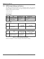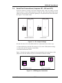
1
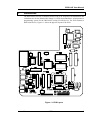
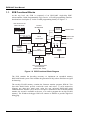
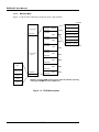
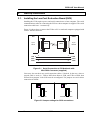
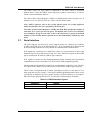
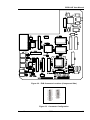
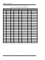
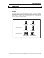
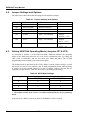
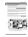
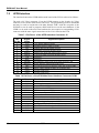
EVB2144F User Manual
EVB2144F
Low-Cost Evaluation Board
User Manual
For H8S/2144F
On-chip FLASH Microcontroller
EVB2144F User Manual
Preface
Product Warranty
The warranty periods against defects in materials and workmanship are as set out in the
accompanying Customer Information sheet.
Limitation of Warranty
The foregoing warranty does not cover damage caused by fair wear and tear, abnormal storage
conditions, incorrect use, accidental misuse, abuse, neglect, corruption, misapplication,
addition or modification or by the use with other hardware or software, as the case may be,
with which the product is incompatible. No warranty of fitness for a particular purpose is
offered. The user assumes the entire risk of using the product. Any liability of Hitachi Micro
Systems Europe Limited is limited exclusively to the replacement of defective materials or
workmanship.
Restrictions
Hitachi Micro Systems Europe Limited's products are not authorised for use in medical
applications without prior written consent. Such use includes, but is not limited to, life support
systems.
Hardware Considerations
1. Earthing
This hardware is designed for use with equipment that is fully earthed. Ensure that all
equipment used is appropriately earthed. Failure to do so could lead to danger for the
operator or damage to equipment.
2. Electrostatic Discharge Precautions
This hardware contains devices that are sensitive to electrostatic discharge. Ensure
appropriate precautions are observed during handling and accessing connections. Failure
to do so could result in damage to the equipment.
3. Electromagnetic Compatibility
Operation of this hardware with any casing removed invalidates the conformity of the
equipment to the Electromagnetic Compatibility Directive 89/336/EEC.
It is advised that in this mode of operation suitable EMC precautions be observed.
Cautions
1. This document may be, wholly or partially, subject to change without notice.
2. All rights reserved. No one is permitted to reproduce or duplicate, in any form, a part or
this entire document without Hitachi Micro Systems Europe Limited's written permission.
Trademarks
1. General
All brand or product names used in this manual are trademarks or registered trademarks of
their respective companies or organisations.
2. Specific
Microsoft, MS and MS-DOS are registered trademarks and Windows and Windows NT are
trademarks of Microsoft Corporation.
IBM is a registered trademark of International Business Machines Corporation.
ProComm® is a registered trademark of Datastorm Technologies.
ii
07/98
Issue 1.0
EVB2144F User Manual
Document Information
Product Code:
MEVB2144F
Version:
1.0
July 1998
Copyright © Hitachi Micro Systems Incorporated. 1994-1995. All rights reserved.
Copyright © Hitachi Micro Systems Europe Ltd. 1995-1998. All rights reserved.
Copyright © Hitachi Europe Ltd. 1995-1998. All rights reserved.
Issue 1.0
07/98
iii
EVB2144F User Manual
Contents
SECTION 1: INTRODUCTION ..............................................................................................................1
SECTION 2: START UP INSTRUCTIONS ..............................................................................................7
SECTION 3: PRINCIPLES OF OPERATION ..........................................................................................13
SECTION 4: BOARD OPTIONS ..........................................................................................................23
SECTION 5: CODE DEVELOPMENT....................................................................................................29
SECTION 6: HDI-MONITOR .............................................................................................................35
SECTION 7: FLASH PROGRAMMING BOARD..................................................................................39
iv
07/98
Issue 1.0
EVB2144F User Manual
Foreword
This document provides information on installing and using the Hitachi H8S/2144F Low-Cost
Evaluation Board (EVB2144F).
Sections 1 to 4
Provide detailed
configuration.
Section 5
Introduces program development using GNU tools.
Section 6
Provides an introduction to HDI-M, the FLASH ROM-resident
debugging program.
Section 7
Provides information on the FLASH programming board.
information
on
hardware
installation
and
For information about the H8S/2144F series microcontrollers, refer to the H8S/2144 Series
Hardware Manual (Hitachi order number: ADE-602-087). For information about the
H8S/2144 assembly language, refer to the H8S/2600, H8S/2000 Series Programming Manual
(Hitachi order number: ADE-602-083).
For EVB hardware and HDI-M support, contact your local Hitachi sales office.
Issue 1.0
07/98
v
EVB2144F User Manual
1.
Introduction
Contents
1. INTRODUCTION ............................................................................................................................. 3
1.1. EVB FUNCTIONAL BLOCKS ...................................................................................................... 4
1.2. SPECIFICATIONS ........................................................................................................................ 5
1.2.1. General ............................................................................................................................ 5
1.2.2. RS-232 Communications ................................................................................................ 5
1.2.3 Power.............................................................................................................................. 5
1.2.4. Memory Map................................................................................................................... 6
Issue 1.0
07/98
1
EVB2144F User Manual
2
07/98
Issue 1.0
EVB2144F User Manual
1.
Introduction
The H8S/2144F low-cost evaluation board (EVB) is an inexpensive demonstration and
evaluation tool for the Hitachi H8S family of 21XX microcontrollers. It incorporates a
programming system for the H8S/2144F on-chip FLASH device. The EVB contains a
H8S/2144F device, Figure 1.1 shows the physical layout of the EVB.
Figure 1.1 EVB Layout
Issue 1.0
07/98
3
EVB2144F User Manual
1.1.
EVB Functional Blocks
At the top level, the EVB is composed of an H8S/2144F single-chip RISC
microcontroller, RAM, Programmable Logic Device, a FLASH programming interface
board and two serial ports (1 via the FLASH programming board), see figure 1.2.
User access to all
MCU I/O Ports
FLASH
INTERFACE
Serial
Interface
Port Interface
RS232 Data
SCI0
I/O PORTS 1-9; A & B
Port 8,0
MCU
H8S/2144F
DATA BUS (16)
ADDRESS BUS (16)
Indicators
Red LED
Reset
ADDRESS BUS (MS4)
NMI,
IRQ0
Port 8,0
Green LED
+5V
0V
Power On
Memory
SRAM
2 x 1Mbit
(128K x 8)
SRAM
Chip
Select
Reset
PLD
EPM/7064STC-7
Power
Supply
Reset
Trigger
User
Switches
External Power
User-controlled Reset
and Interrupts
(CRES, NMI, IRQ0)
Figure 1.2 EVB Functional Block Diagram
The PLD contains the decoding necessary to implement an expanded memory
H8S/2144F-based system. This includes the generation of chip selects and discrete signal
de-bouncing.
The on-chip FLASH memory contains the firmware monitor program, HDI-M. Two
byte-wide RAM blocks provide word-wide reads and writes. A serial transceiver
supports two three-wire serial ports using the two on-board H8S/2144F serial
communications interface (SCI) devices. One port is dedicated to the on-board HDI-M
monitor, the second is available to the user, or is used to program the on-chip FLASH
memory. The Windows debugger HDI will connect to HDI-M to provide high-level
debugging.
4
07/98
Issue 1.0
EVB2144F User Manual
Users reconfiguring the EVB I/O-ports are cautioned that pull-up resistors may be
required for proper operation in some configurations. In particular, users adding external
memory in areas 1 through 7 should be aware that chip selects 1-7 provided by the PLD
are decoded from the address lines and may be floating until the system is configured. In
addition, when connecting external analogue signals, it is important that the EVB is
configured properly with respect to analogue voltage supply and reference (jumpers J5
to J7).
1.2.
Specifications
1.2.1.
•
•
•
•
•
•
1.2.2.
•
•
Issue 1.0
RS-232 Communications
Host interface via RS-232 DB-9S connector
User interface via RS-232 DB-9S connector
1.2.3.
•
•
General
20MHz H8S/2144F processor (using HD64F2144F20 device)
256Kbytes of RAM, accessed in 16-bit words
128Kbytes of FLASH with the HDI-M firmware monitor
Two LED indicators and three push button switches
Detachable FLASH programming interface board
All practical H8S/2144F signals available for user connection
Power
5V DC-only power supply
Power connection via 4mm standard plugs
07/98
5
EVB2144F User Manual
1.2.4.
Memory Map
Figure 1.3 shows the EVB memory maps for mode 2 (the default).
H’020000
H’000000
256kbytes SRAM
H’020000
On-Chip ROM
CSRAM0
256k Shadowed SRAM
1.7Mb
H’1FFFFF
256k Shadowed SRAM
H’200000
CS1
H’01FFFF
H’020000
2MB
H’3FFFFF
256k Shadowed SRAM
256k Shadowed SRAM
H’400000
CS2
2MB
H’5FFFFF
256k Shadowed SRAM
256k Shadowed SRAM
H’600000
CS3
2MB
CS4
2MB
CS5
2MB
CS6
2MB
CS7
1MB
H’1FFFFF
H’7FFFFF
External Address
Space
H’800000
H’9FFFFF
H’A00000
H’BFFFFF
On-Chip
RAM*
External
Address Space
Internal I/O
Registers 2
On-Chip
RAM*
Internal I/O
Registers
H’C00000
H’DFFFFF
H’FFE080
H’E00000
H’EFFFFF
NOTES: *On-Chip RAM can be used as external address space by
clearing the RAME bit in the SYSCR to 0.
Figure 1.3 EVB Memory Map
6
07/98
Issue 1.0
EVB2144F User Manual
2.
Start Up Instructions
Contents
2. START UP INSTRUCTIONS ............................................................................................................. 9
2.1. INSTALLING THE LOW-COST EVALUATION BOARD (EVB) ...................................................... 9
2.2. POWER SUPPLY........................................................................................................................ 10
2.2.1. Power Connection......................................................................................................... 10
2.3. SOFTWARE INSTALLATION ...................................................................................................... 10
2.3.1. Installation of CD-ROM software ................................................................................ 10
2.3.2. DOS Setup .................................................................................................................... 11
2.3.3. Verifying GNU Installation .......................................................................................... 11
Issue 1.0
07/98
7
EVB2144F User Manual
8
07/98
Issue 1.0
EVB2144F User Manual
2.
Start-Up Instructions
2.1.
Installing the Low-Cost Evaluation Board (EVB)
Installing the EVB requires power and serial connection to a host computer. The serial
communications cable for connecting the EVB to a host computer is supplied. The serial
connection cable has 1:1 connectivity.
Figure 2.1 shows how to connect the EVB to a PC or notebook computer equipped with
a “mini” DB-9P connector.
EVB
PC
9-pin
DB-P
9-pin
DB-9S
DB9P
DB9S
3
3
RXD
2
2
RXD
GND
5
5
GND
TXD
TXD
Figure 2.1 Serial Connection to PC/Notebook with
Mini DB-9 Connector (supplied)
Users may also use their own serial connection cables, if desired. In the case, where a
crossed cable is used (i.e. TXD to RXD from Host to EVB, and TXD to RXD from
EVB to Host) jumpers J4 for SCI0 must be reconfigured. The jumpers are set for direct
connection as default.
J4
J4
U6
U6
Crossed Connection
1:1 Connection
Figure 2.2 Jumper settings for SCI0 connections
Issue 1.0
07/98
9
EVB2144F User Manual
2.2.
Power Supply
The EVB hardware requires a power supply of +5V at approximately 250mA supplied
to CON9. Since total power consumption can vary widely due to external connections,
H8S/2144F port state, and memory configuration, use a power supply capable of
providing at least 600mA at +5V DC ± 5%.
1
Caution: A power supply with current limiting and an active current display is
recommended when the EVB is used for hardware experimentation. The EVB is
provided with polarity reversal protection. If the EVB does not consume any
current, check the power connection for polarity reversal.
2.2.1.
Power Connection
The power connector on the EVB is connected to 4mm sockets mounted in the casing.
Standard 4mm plugs may be used to connect to a bench power supply.
2.3.
Software Installation
Please review the following procedures thoroughly before installing. Software is
supplied with the EVB on a CD-ROM. Users should make sure their system has a CDROM drive correctly installed before continuing.
The EVB includes software in five parts:
1.
2.
3.
4.
5.
HDI-M Windows debugger
Hitachi Workbench (HWB) and IAR C Compiler (limited versions)
FLASH programming interface and code examples.
EVB Tutorials and supplementary tools.
GNU Tools
2.3.1.
Installation of CD-ROM software
An installation utility is supplied with the CD-ROM, enabling the user to easily install
all components of the EVB2144F. In addition, each main software package has its own
installation utility to enable separate installation. For using the main installation utility,
please refer to the CD-ROM insert.
To install the components listed above, please note the locations of the setup utilities:
•
•
•
•
•
HDI-M Windows debugger
HWB & IAR C Compiler
GNU Tools
FLASH programming interface
Tutorials and supplementary tools:
D:\HDIM\SETUP.EXE
D:\HWBDEMO\SETUP.EXE
D:\GNU\H8_97r1a\INSTALL.EXE
D:\FLASH\SETUP.EXE
D:\TUTORIAL\INSTALL.EXE
Note: The default installation directory for the tutorial files is c:\HWBDEMO\
TUTORIALS\… as used in the tutorial.
10
07/98
Issue 1.0
EVB2144F User Manual
2.3.2.
DOS Setup
The GNU tools include a file named SETENV.BAT that must usually be executed
before the tools are used. The contents of this file may be copied to AUTOEXEC.BAT
as described in the Cygnus support tools Installation Notes.
One of the SET commands in SETENV.BAT is:
SET GO32=C:\CYGNUS\BIN\EMU387
or similar, depending on your installation path. You may wish to add an additional
directive to this to redirect DOS stderr to stdout, so that you may redirect GNU tools
error outputs to DOS files.
The modified line will look like the following:
SET GO32=EMU C:\CYGNUS\BIN\EMU387 2r1
No special setup is required by the supplementary tools and tutorials.
2.3.3.
Verifying GNU Installation
To verify GNU tools installation, execute the setup batch file, set the current directory
to DEMO, and execute GNU make, for example as follows:
C:\> c:\cygnus\setenv
C:\> cd \cygnus\demo
C:\cygnus\demo> make
run hello.x
Hello World 0
Hello World 1
...
Hello World 9
This confirms that essential portions of the GNU tools are correctly installed.
Issue 1.0
07/98
11
EVB2144F User Manual
12
07/98
Issue 1.0
EVB2144F User Manual
3.
Principles of Operation
Contents
3. PRINCIPLES OF OPERATION ....................................................................................................... 15
3.1.
H8S/2144F MICROCONTROLLER .................................................................................... 15
3.2.
CLOCK CIRCUITRY ........................................................................................................... 15
3.3.
COLD RESET CIRCUITRY .................................................................................................. 15
3.4.
NMI CIRCUITRY ............................................................................................................... 16
3.5.
INTERRUPT REQUEST CIRCUITRY .................................................................................... 16
3.6.
RAM................................................................................................................................. 16
3.7.
SERIAL INTERFACE ........................................................................................................... 17
3.8.
LED DRIVER .................................................................................................................... 18
3.9.
EXTERNAL USER INTERFACE ........................................................................................... 18
Issue 1.0
07/98
13
EVB2144F User Manual
14
07/98
Issue 1.0
EVB2144F User Manual
3.
Principles of Operation
The EVB is composed of the following components:
•
•
•
•
•
•
•
•
•
•
•
H8S/2144F microcontroller
Clock circuitry
Cold Reset (CRES) circuitry
NMI circuitry
IRQ0
On-board RAM
Detachable Programming Interface board
Serial interfaces
LED driver
External user interface
PLD
The complete EVB schematics are provided as part of the EVB kit and are referenced
throughout this chapter.
3.1.
H8S/2144F Microcontroller
The H8S/2144F provides on-chip many of the functions required to implement an
expanded-memory microcontroller system. The address area decoding is performed by a
PLD. Users reconfiguring processor I/O ports are cautioned that pull-up resistors may
be required for proper operation in some configurations. In particular, users adding
external memory should be aware that the chip selects provided by the PLD are shared
and may be floating until the system is configured.
3.2.
Clock Circuitry
The clock circuitry comprises the H8S/2144F oscillator and an external 18.432MHz
AT-cut parallel resonating crystal. The system clock (CLKOUT pin) output frequency is
the same as that of the internal clock.
3.3.
Cold Reset Circuitry
The reset generator for the EVB is based on the 7705A Supply Voltage Supervisor from
Texas Instruments or SGS Thomson. This chip is specifically designed for use as a reset
controller in microcomputer and microprocessor systems.
During power-up the device monitors the supply voltage and keeps the RESET and
RESET* outputs active (high and low respectively) as long as the supply voltage has
not reached its nominal value. After the voltage has reached the tolerance, the RESET
and RESET* are kept active for an additional 60ms to allow for final supply
stabilisation and processor reset. Specifically the H8S/2144F needs up to 10ms for the
crystal oscillator to stabilise.
The threshold voltage is 4.5V ± 50mV with a hysteresis of 15mV. If there is a voltage
drop on the supply the RESET* will be activated. When the supply recovers and passes
the threshold the RESET* is not released for another 60ms.
Issue 1.0
07/98
15
EVB2144F User Manual
There is also a push-button switch SW1 to generate a manual cold reset (CRES*). The
switch is debounced within the PLD and fed to the RESIN*-input of the 7705A. When
the push-button is released the 7705A will provide a 60 ms reset signal.
The de-bounced CRES output is ORed with the FLASH_RES* signal from the flash
programming board to generate the final RESET* signal to the CPU when FLASH
programming. This RESET* signal is also fed back to the flash programming board. If
the programming board is not present there is a pull-up resistor to deactivate the
FLASH_RES* signal.
In loader mode the CRES will reset the entire board and start the bootloader program
running. Therefore, a new s-record must be downloaded to the H8S/2144F.
Quickly switching power to the board off and then on again quickly may not allow VCC
to fall low enough to generate a reset pulse. In practice, the H8S/2144F usually
continues to operate normally. Rapid on/off switching of the power supply stresses the
integrated circuit components and is not recommended.
3.4.
NMI Circuitry
The NMI input of the H8S/2144F is an independent edge-triggered input. NMI may be
generated on the positive or negative-going transition, depending on the setting of the
Interrupt Control Register (ICR) NMIEG bit. Default after reset is negative going edge.
On the EVB there is a push-button switch SW2 that is debounced within the PLD to
generate the NMI-signal. The quiescent state is low and when SW2 is pressed the NMI
goes high. When SW2 is released the NMI will return to low level and generate a
negative-going edge.
The NMI signal can alternatively be driven from an external source, the PLD has an
open drain output to control the NMI signal and as such an external source can be used
without any alteration to the EVB configuration.
3.5.
Interrupt Request Circuitry
When the board is in Run mode in which the downloaded program is being executed the
IRQ0 switch (SW3) will cause the H8S/2144F to interrupt the operation of the program.
The contents of the external SRAM are not lost by this operation.
3.6.
RAM
The EVB’s RAM is located at U4 and U5, which contain a pair of 128kx8 628128family static CMOS RAM organised for word-wide access. Figure 1.3 (section 1) shows
the memory map.
The external RAM is normally located at H’0x20000 - H’0x60000 in CS0 space. The
total memory available for the user is 256Kbytes. This is “shadowed” for area 0. This
means that, when accessing the higher address ranges in area 0, it actually writes to the
same memory devices as the lower addresses. When RAM is referenced at this address,
the memory area chip select signal CS0*, RD* or WRL* or WRH* are generated by the
H8S/2144F. CS0* and RD* signal are connected to both U4 and U5.
16
07/98
Issue 1.0
EVB2144F User Manual
The WRL* (write low byte) signal is connected to U4 device which is connected
databus D0-D7 while the WRH* (write high byte) signal is connected to U5 device
which is connected databus D8-D15.
The value of Bus Control Register 1 (BCR1) bit A0SZ specifies the CS0 space size. It
should be set to 1 to specify 16-bit size. This is also the default value.
Note: A0SZ is effective only in the on-chip effective mode. In on-chip ineffective
mode, the CS0 space bus size is specified by the mode pins.
The value of Wait Control Register 1 (WCR1) bits W00-W03 specifies the number of
wait-states (0-15 cycles) for the CS0 space. The default value is B’1111. It should be
set to B’0000 to specify no wait. This is due to the selected access speed of the RAM
memory of 55ns and this makes it possible access the RAM memory without any waitstates.
3.7.
Serial Interface
The EVB supports two three-wire serial channels using two identical SCI modules
(UARTs) SCI0 and SCI1 in the H8S/2144F CPU. SCI1 is normally the USER port and
SCI0 is normally dedicated to use by HDI-M for communications with a host PC.
SCI0 signals are connected to U6 (MAX232) which is a serial transceiver device that
translates logic levels to RS-232 levels and vice-versa. The RS-232 signal for the USER
port is connected to J4 which is a DB-9S type connector.
SCI1 signals are routed via the flash programming board. Normally the host terminal
communication is done via the H8/3217 device on the flash programming board.
On this board the U4 (MAX232) transceiver circuit translates to RS-232 levels. The RS232 signals for the HOST port is connected to CON10 that is a DB-9S type connector.
There is also a transparent mode in which serial data just passes via the H8/3217. For
more about this, refer to Section 7, Universal FLASH Programming Board. There is also
a possibility to hardwire the SCI1 signals directly to RS-232 transceiver via jumpers,
thus effectively bypassing the H8/3217. See Section 4, Board Options for details.
Table 3.4 RS232 Interface Signals
Connector
CON10
J4
Issue 1.0
Signals
SCI0
SCI1
07/98
17
EVB2144F User Manual
3.8.
LED Driver
There are two LED’s on the EVB to display board status. The first LED is red and
indicates when power is supplied to the EVB. The second is green and can be driven,
using port 8, bit 0 of the H8S/2144F.
3.9.
External User Interface
The external user interface makes most H8S/2144F signals available to user consistent
with keeping:
•
•
•
•
Signal lines short
Board design simple
Functional signals grouped together
Lines potentially used for analog signals isolated
The external user interface consists of seven two-row connectors of 20 pins each.
Commonly available 2.54mm (0.100 inch) male headers with 0.635mm (0.25 inch)
square posts may be used.
Table 3.6 Address and Data Connectors and Signals
Connector
Signals
CON2
Address Bus 0 to 15.
CON3
Port 5 0 to 2 / STBYn / NMIn / RESOn / Port 8 0 to 6.
CON4
Address Bus 16 to 23 / Control bus 5 to 12.
CON5
Data Bus 0 to 15.
CON6
Port 4 0 to 7 / Port 6 0 to 7
CON7
Port 7 0 to 7 / AVcc / AVref / Avss
CON8
Port 9 0 to 7
Note: Each of these external interface connectors also includes VCC, normally at +
5V and GND. Trivial external circuits may use the power from EVB. However, if
more than 50mA is needed the external circuits should be powered by an independent
power supply.
Since CON7 may carry analogue signals, each analogue signal is alternated with a
separate analogue ground signal.
Figure 3.2 shows the board locations of these connectors CON2 – CON8. Note the
positioning of pin 1 on each connector. The pins are numbered odd-even as shown in
Figure 3.3.
18
07/98
Issue 1.0
EVB2144F User Manual
Figure 3.2 EVB Connector Locations (Component Side)
1
3
5
7
9
11
13
15
17
19
2
4
6
8
10
12
14
16
18
20
1
3
5
7
9
11
13
15
2
4
6
8
10
12
14
16
Figure 3.3 Connector Configuration
Issue 1.0
07/98
19
EVB2144F User Manual
Table 3.7 describes each user connector CON2 to CON5 in numerical order.
Table 3.7 Connectors CON2 to CON5 Pinout
Pin
1
20
CON2
Signal
P1(0)
Pin
1
CON3
Signal
P5(0)
Pin
1
CON4
Signal
PA(0)
Pin
1
CON5
Signal
PB(0)
2
P2(0)
2
P8(0)
2
AVss_Ext
2
P3(0)
3
P1(1)
3
P5(1)
3
PA(1)
3
PB(1)
4
P2(1)
4
P8(1)
4
AVss_Ext
4
P3(1)
5
P1(2)
5
P5(2)
5
PA(2)
5
PB(2)
6
P2(2)
6
P8(2)
6
AVss_Ext
6
P3(2)
7
P1(3)
7
STBYn
7
PA(3)
7
PB(3)
8
P2(3)
8
P8(3)
8
AVss_Ext
8
P3(3)
9
P1(4)
9
NMIn
9
PA(4)
9
PB(4)
10
P2(4)
10
P8(4)
10
AVss_Ext
10
P3(4)
11
P1(5)
11
RES0n
11
PA(5)
11
PB(5)
12
P2(5)
12
P8(5)
12
AVss_Ext
12
P3(5)
13
P1(6)
13
Vcc
13
PA(6)
13
PB(6)
14
P2(6)
14
P8(6)
14
AVss_Ext
14
P3(6)
15
P1(7)
15
Vcc
15
PA(7)
15
PB(7)
16
P2(7)
16
GND
16
AVss_Ext
16
P3(7)
17
Vcc
17
Vcc
17
AVRef_Ext
17
Vcc
18
GND
18
GND
18
AVss_Ext
18
GND
19
Vcc
19
Vcc
19
AVcc_Ext
19
Vcc
20
GND
20
GND
20
AVss_Ext
20
GND
07/98
Issue 1.0
EVB2144F User Manual
Table 3.8 describes each user connector CON6 to CON8 in numerical order.
Table 3.8 Connectors CON6 to CON8 Pinout
Pin
1
Issue 1.0
CON6
Signal
P4(0)
Pin
1
CON7
Signal
P7(0)
Pin
1
CON8
Signal
P9(0)
2
P6(0)
2
AVss
2
GND
3
P4(1)
3
P7(1)
3
P9(1)
4
P6(1)
4
AVss
4
GND
5
P4(2)
5
P7(2)
5
P9(2)
6
P6(2)
6
AVss
6
GND
7
P4(3)
7
P7(3)
7
P9(3)
8
P6(3)
8
AVss
8
GND
9
P4(4)
9
P7(4)
9
P9(4)
10
P6(4)
10
AVss
10
GND
11
P4(5)
11
P7(5)
11
P9(5)
12
P6(5)
12
AVss
12
GND
13
P4(6)
13
P7(6)
13
P9(6)
14
P6(6)
14
AVss
14
GND
15
P4(7)
15
P7(7)
15
P9(7)
16
P6(7)
16
AVss
16
GND
17
Vcc
17
AVcc
17
Vcc
18
GND
18
GND
18
GND
19
Vcc
19
AVref
19
Vcc
20
GND
20
GND
20
GND
07/98
21
EVB2144F User Manual
22
07/98
Issue 1.0
EVB2144F User Manual
4.
Board Options
Contents
4. BOARD OPTIONS ......................................................................................................................... 25
4.1.
JUMPERS ........................................................................................................................... 25
4.2.
JUMPER SETTINGS AND OPTIONS ..................................................................................... 26
4.3.
SETTING H8S/2144 OPERATING MODE (JUMPERS JP1 & JP2) ....................................... 26
4.4.
PORT 9 PULL-UP JUMPER (JP3) ....................................................................................... 27
4.5.
SERIAL PORT CONNECTIONS (JUMPER JP4 ).................................................................... 27
4.6.
ANALOGUE REFERENCE AND SUPPLY (JUMPERS JP5 TO JP7)......................................... 27
Issue 1.0
07/98
23
EVB2144F User Manual
24
07/98
Issue 1.0
EVB2144F User Manual
4.
Board Options
The EVB provides a number of user-definable optional configurations. Some of these
are chosen by jumper settings or configuration via zero Ohm resistors, while others use
alternative loading options.
4.1.
Jumpers
EVB jumpers allow users to configure the board as required for testing or evaluation.
The jumpers come in three types: 2 or 3 pin in-line for a single jumper or 2 by 2 pin for
1 or 2 jumper capacity. The three-pin in-line jumpers are used to connect one of two
possible signals to a third line, the 4-pin blocks typically allow signal paths to be
changed by rotating the jumpers through 90º.
2-pin Jumper Setting
Jumper present
3-pin Jumper Setting
Jumper removed
1
1
2
2
3
3
1-2 Connection
2-3 Connection
2
4
2
4
1
3
1
3
4-pin Jumper Setting
Normal orientation
Rotated through 900
Figure 4.1 Jumper settings
Issue 1.0
07/98
25
EVB2144F User Manual
4.2.
Jumper Settings and Options
The table below shows the different settings for the different jumpers.
Table 4.1 Jumper Settings and Options
Jumper
JP1
JP2
JP3
JP4
JP5
4.3.
Use
H8S/2144 MD0
H8S/2144 MD1
Port 9 pull-up
SCI jumper
AVREF
1-2
default- sets 2144
default- to Mode 0
Fitted – bits 0 to 2 = 5V
Open - set externally
JP6
AVCC
Open - set externally
JP7
AVSS
Default- AVSS = VSS
2-3
defaultAVREF = VCC
defaultAVCC = VCC
Open –
AVSS = 0V
Setting H8S/2144 Operating Mode (Jumpers JP1 & JP2)
As described in Section 3 of the H8S/2144 RISC Hardware Manual, the operating
modes of the H8S/2144 processor are set at device initialisation time by setting pin
FWE (VPP in schematic) and the two mode pins MD0 and MD1. The FLASH
programming board normally sources the FWE signal.
The default mode of operation for the EVB is Mode 2 but the jumper setting is a weak
pull down so it may be over-ridden by the FLASH programming board without having
to change or cut any default jumpers. For ease of change, jumpers JP1 and JP2 are
equipped with pin-headers. Table 4.2 shows MCU operating mode settings.
Table 4.2 MCU Mode Settings
Operating Mode
0
1
2*
3
Jumper Setings
JP2 (MD1)
0
0
1
1
JP1 (MD0)
0
1
0
1
* The default-selected mode will be over-ridden automatically by the programming
board.
At power-up or CRES* (cold reset), Mode 2 (NORMAL) will be selected.
26
07/98
Issue 1.0
EVB2144F User Manual
4.4.
Port 9 Pull-Up Jumper (JP3)
To allow FLASH programming of H8S/2144F, port bits 0 to 2 must be pulled up to
+5V. The jumper allows the user to remove the pull-up and drive the port pins.
4.5.
Serial Port Connections (Jumper JP4 )
SCI0 (UART0) is dedicated by default to the monitor for the HOST port and the SCI1
(UART1) is dedicated to USER port via the programming board. The port pins (TXD0,
RXD0, TXD1 and RXD1) associated with transmitting and receiving data for UARTs
are connected to serial transceiver circuits.
4.6.
Analogue Reference and Supply (Jumpers JP5 to JP7)
Port H of the H8S/2144 may be configured for analogue inputs. In this case, reference
voltages for the analogue signals become important. The default setting of these three
jumpers connect on-board digital references and the digital VCC for the analogue
subsystem in the H8S/2144 processor. For most demonstration purposes, this
configuration may be sufficient. However, to demonstrate the full capabilities of the
H8S/2144 analogue subsystem, as well as to reduce noise in the analogue part, it may be
desirable to use external sources for some or all of these signals.
The recommended decoupling capacitors are provided on the reference circuits as
recommended by the H8S/2144 hardware manual, Section 14.6.
If an external analogue reference voltage (AVREF) is provided to the H8S/2144 on the
J3-37, set JP5 to 1-2.
If an external analogue VCC (AVCC) is provided to the H8S/2144 on the J3-35, set JP6
to 1-2.
If an external analogue ground (AVSS) is provided to the H8S/2144 on the J3-1, set JP7
to 2-3.
Any of these jumpers may not be left open.
Issue 1.0
07/98
27
EVB2144F User Manual
5.
Code Development
Contents
5.
CODE DEVELOPMENT ........................................................................................................... 31
5.1
HOST COMPUTER SPECIFICATIONS ...................................................................................... 31
5.2
GNU TOOLS ......................................................................................................................... 31
5.3
TUTORIALS ........................................................................................................................... 32
5.4
ADDITIONAL INFORMATION ................................................................................................. 33
Issue 1.00
07/98
29
EVB2144F User Manual
30
07/98
Issue 1.00
EVB2144F User Manual
5.
Code Development
The H8S/2144F EVB is supplied with the HWB/IAR limited and GNU tools for
H8S/2144F (the standard development tools for the EVB). Hitachi also makes full
versions of the HWB/IAR tools available for H8S/2144F development (an extra-cost
option).
When debugging programs developed for use with the EVB, use the HDI-M debugger
—stored in FLASH— with the HDI Windows GUI. HDI supports either the GNU tools
or the IAR tools.
5.1
Host Computer Specifications
For program development with the EVB package, you will need:
•
•
•
•
•
•
5.2
A computer capable of hosting the Windows tools, editing files, and
communicating with the evaluation board. The computer must be an i486 standard
PC running DOS 5.0 or higher and Windows 95.
640 kbytes of base memory. Additional extended memory of at least 16Mbytes is
highly recommended.
A hard disk; the Windows tools require 10-15Mbytes or more hard disk space. The
supplementary tools and tutorials files require only a small amount of space.
A CD-ROM drive. The tools and tutorials are distributed on a single CD-ROM.
A standard serial port, COM1 or COM2, is required for host computer
communication with the EVB2144F.
The GNU tools require a text editor capable of editing program source files without
inserting non-printing characters in the file. An ASCII editor such as DOS EDIT is
acceptable.
GNU Tools
GNU refers to a powerful set of operating system and software development tools
developed in the style of, but independently from, the UNIX™ environment and made
available on a variety of host computers for many different target devices. The source
code to all GNU software is available at little or no cost. All GNU software is provided
under the Free Software Foundation’s “copyleft.” HDI-M supports the GNU debugging
format.
The GNU tools for the EVB2144F are provided by Cygnus Support, a vendor of
commercial support for GNU tools. Please refer to the documents in the Cygnus Support
Developer’s Kit, included in the EVB2144F package, especially Release Notes and
Installation Notes, for a complete description of the nature and parameters of GNU
software. GNU tools to be installed are described in the initial section of the Cygnus
Support Installation Notes supplied as part of the EVB2144F kit.
Issue 1.00
07/98
31
EVB2144F User Manual
For the purposes of this document, it is most important to make clear that the GNU tools
provide a comprehensive software development environment for the H8S/2144F,
including:
•
C compiler, gcc
•
Assembler, as
•
Linker/loader, ld
•
Library archiver, ar
•
Interactive debugger, gdb
•
Additional utilities, such as nm and make
The GNU tools may be used to develop C programs of any length and run them on the
EVB, subject to RAM availability.
The current release of the GNU tools accompanying the EVB is valid only for DOS.
There are no corresponding releases for alternative platforms. Users familiar with UNIX
style and programming practices may derive additional benefit from using the GNU
tools, but it is not necessary to know UNIX to use the GNU tools.
5.3
Tutorials
The separate tutorial manual has more information on installing and using the Hitachi
Windows tools to do simple program development and demonstrations on the EVB.
Subjects include preparing and running:
•
A program that turns the green LED on and off
•
A “hello world” demonstration
•
A program that flashes the green LED
The Tutorial manual includes information on developing code that makes use of the onchip peripherals of the H8S/2144F and provides examples of initialisation of static data.
These examples provide more in-depth information on the use of IAR compiler
extensions, interfacing to assembler and use of linkage control files. Subjects include:
•
•
•
•
A simple program with startup code for initialisation of static data
A program to provide serial I/0 using SCI0
A program using timed interrupts to flash the green LED while providing serial I/O
on SCI0.
A program which may be programmed into FLASH, to replace HDI-M,
highlighting the steps required to create real application code
The Tutorial manual details the use of the on-chip FLASH of the H8S/2144F. The
examples enable users to program the on-chip FLASH using the programming board
and Windows interface software.
32
07/98
Issue 1.00
EVB2144F User Manual
The Tutorials section includes:
•
•
•
•
5.4
Overview of FZTAT operation
Programming board and interface software usage
Programming tutorials from The Tutorial section into the on-chip flash
Understanding the operation of the BOOT and USER mode kernels
Additional Information
For details on how to use HDI-M, the EVBs resident debugger, refer to the HDI-M
manual supplied with the EVB.
For information about the H8S/2144F series microcontrollers, refer to the H8S/2144F
Series Hardware Manual (Hitachi order number: ADE-602-087).
For information about the H8S/2144F assembly language, refer to the H8S/2600 Series,
H8S/2000 Series Programming Manual (Hitachi order number: ADE-602-083).
For more information about the GNU tools refer to the Cygnus Support Release Notes
and Installation Notes, the HTML GNU manuals, including Using GNU CC, Using as,
Using ld, and Debugging with gdb; and the on-line help browser tool, info.
This document is not intended to be a tutorial on embedded system programming in
general, C language, or the GNU tools.
The standard reference book on the C language is The C Programming Language, by
Brian W. Kernighan and Dennis M. Ritchie, Prentice-Hall, 1978.
Issue 1.00
07/98
33
EVB2144F User Manual
34
07/98
Issue 1.00
EVB2144F User Manual
6.
HDI Monitor
Contents
6. HDI-MONITOR......................................................................................................................... 37
6.1 INTRODUCTION TO HDI-M ....................................................................................................... 37
6.2 PROGRAM DEVELOPMENT ........................................................................................................ 37
6.3 USING HDI-M........................................................................................................................... 37
Issue 1.00
07/98
35
EVB2144F User Manual
36
07/98
Issue 1.00
EVB2144F User Manual
6.
HDI-Monitor
6.1
Introduction to HDI-M
HDI-M is a FLASH-resident debugging monitor program hosted on the EVB. HDI-M
may be used to download, run, and debug programs developed on a host PC-compatible
computer. HDI-M provides all the necessary control and communications to operate
under the HDI GUI. This allows users to perform high level C debugging on the EVB.
Using HDIs powerful debugging features, users may explore features of the H8S/2144F
processor and the EVB by directly entering and running simple programs.
Install HDI-M from the CD-ROM, as described in Section 2.
6.2
Program Development
The tutorials contain several examples you may use to explore and evaluate the
H8S/2144F architecture. You need not install the HWB/IAR limited or GNU tools
unless you are doing additional program development. Any tool chain that produces
absolute H8S/2144F code in Motorola S-record format may be used with HDI-M. In
addition, HDI-M supports the GNU-coff, Hitachi-SYSROF and IAR-UBROF formats.
6.3
Using HDI-M
HDI-M is a free monitor for use with the evaluation boards. A manual in PDF format is
supplied on the CD-ROM that covers installation and basic usage. The tutorials, in the
separate tutorials manual, are specifically designed to cover embedded code
development, and are not intended as a tutorial on using HDI-M. Please refer to the
HDI-M manual for further information.
Issue 1.00
07/98
37
EVB2144F User Manual
38
07/98
Issue 1.00
EVB2144F User Manual
7.
Universal FLASH Programming Board
Contents
7.
UNIVERSAL FLASH PROGRAMMING BOARD ..................................................................... 41
7.1
PROGRAMMING BOARD OPERATION ................................................................................... 41
7.2
UFPB INTERFACE ................................................................................................................ 42
7.3
UFPB OPERATION ............................................................................................................... 43
7.4
TRANSPARENT MODE AND THE PMODE PIN ...................................................................... 43
7.5
OPERATION DURING H8S/2144F INITIALISATION TO BOOT,
USER & NORMAL MODES ................................................................................................... 44
7.6
OPERATION DURING PROGRAMMING KERNEL EXECUTION ................................................. 45
7.7
PROGRAMMING SOFTWARE OPERATION ............................................................................. 45
7.8
UFPB JUMPER SETTINGS AND OPTIONS .............................................................................. 46
7.9
SERIAL PORT CONNECTIONS (JUMPERS JP1, JP2 AND JP3) ................................................ 47
7.10 FWE/FWP CONTROL (JUMPER JP4) ................................................................................... 48
7.11 MDX CONTROL (JUMPER JP5)............................................................................................. 48
Issue 1.00
07/98
39
EVB2144F User Manual
40
07/98
Issue 1.00
EVB2144F User Manual
7.
Universal FLASH Programming Board
7.1
Programming Board Operation
The Universal Flash Programming Board (UFPB) is a plug-in module which is capable
of providing the control signals and voltages required to place an H8S/2144F into
BOOT, USER or normal execution mode without requiring the user to touch the EVB.
The programming board has been designed to allow users to test the features of the onchip FLASH, without having to worry about any hardware requirements. In addition it
may be unplugged from the EVB2144F main board, and connected to a user’s system
using a 14-pin interface (specified in table 7.2). This allows users to evaluate In-SystemProgramming (ISP) of the H8S/2144F without having to construct additional circuitry.
Figure 7.1 shows the physical layout of the UFPB.
Note: Using the programming board outside of the enclosure supplied invalidates the
conformity to the EMC directive (89/336/EEC). It is advised that in this mode of
operation, suitable EMC precautions are taken.
Note: The programming board as supplied with the EVB kit, is for prototype use only.
It should not be used in mass production to program devices.
Figure 7.1 Universal programming Board Layout
Issue 1.00
07/98
41
EVB2144F User Manual
7.2
UFPB Interface
The interface between the UFPB and the main board of the EVB is achieved as follows:
The male (2x7 Way) connector J5 on the UFPB connects to the female (2x7 Way)
connector CON1 on the main board of the EVB. The programming board is detachable
and may be used in conjunction with other Hitachi EVB’s with the exception of the
EVB7050 or can be used to program a H8S/2144F device on the users hardware. If the
UFPB is to be used on the users own hardware the user requires a corresponding CON1
connector with the same signal connections of the CON1 fitted on the EVB.
Table 7.1 Pin Descr. of the UFPB Interface Connector J5
JP5
Pin No.
1
2
3
4
5
6
7
8
9
10
11
12
13
14
Signal
Name
VCC
GND
RX
TX
WRES*
CRES*
Vpp
MDx
PMODE
RESET*
FWP
MDy
GND
GND
Signal Description
+5V supply input to UFPB
Ground reference input to UFPB
Output data to main board of EVB
Input data from main board of EVB
Warm reset input from main board of EVB
Cold reset input from main board of EVB
Not used
Not used
Programming mode input from main board of EVB
Reset output to main board of the EVB
FLASH Write Protect output to FWP pin of H8S/2144F
Mode control output to MD1 pin of H8S/2144F
Ground connection
Ground connection
Table 7.2 Pin Descr. of the EVB Main Board Interface Connector CON1
CON1
1
2
3
4
5
6
7
8
9
10
11
12
13
14
42
Name
GND
VCC
TX
RX
CRES*
WRES*
RESET*
PMODE
MDy
FWE
GND
GND
Function
Ground reference connection to UFPB
+5 V supply connection to UFPB
Output data to UFPB
Input data from UFPB
Cold reset output to UFPB
Warm reset output to UFPB
Not used
Not used
Reset (active low) to H8S/2144F
Programming mode output to UFPB
Mode pin H8S/2144F
FLASH Write Enable signal to H8S/2144F
Ground connection
Ground connection
07/98
Issue 1.00
EVB2144F User Manual
Figure 7.1 below shows the placement and pin numbering system for the CON1
connector on the EVB.
1 3
13
9.0 mm to
board end
2.54 mm
2 4
14
0.9 mm
2.54 mm
Figure 7.1 Placement and Pin-numbering of the CON1 connector on the
EVB
The CON1 connector used on the EVB is a double row, right angle receptacle from
Samtec, order code SSW 107 02 T D RA.
7.3
UFPB Operation
The H8S/3217 on the UFPB board allows the Windows FLASH programming interface
to dynamically control all aspects of the boards operation. The RS-232 connection is
used to communicate between the H8S/3217 and the host PC. The H8S/3217 also
connects to the SCI1 of the H8S/2144F during programming for data and command
transfer.
Please note: This type of board is not required for an end-user system, it has been
designed by Hitachi to be as flexible as possible. The application note supplied details
how to implement FLASH programming within the user’s system.
Note: The programming board that you received in your kit can be modified to
program other Hitachi FLASH devices.
As detailed in section 7.8 the H8S/3217 may be bypassed using jumpers JP2 and JP3 to
allow the H8S/2144F to directly access the RS-232 port on the programming board
when the user does not wish to program the FLASH memory on the device.
7.4
Transparent Mode and the PMODE pin
The final operation performed during initialisation is to place the programming board
into transparent mode. In this mode any character received from the Host is retransmitted directly to the H8S/2144F and vice-versa with no processing. The H8S/3217
effectively stops command processing, and will not resume unless reset, or signalled by
the H8S/2144F via the PMODE pin (Port 8 pin 1).
Issue 1.00
07/98
43
EVB2144F User Manual
During normal command processing, the PMODE signal is ignored. The programming
kernel that is downloaded to the H8S/2144F takes this pin LOW during initialisation.
During transparent mode, the H8S/3217 checks the status of the PMODE signal, if this
is taken HIGH, the H8S/3217 leaves transparent mode. This operation is performed by
the programming kernel during disconnect.
If users wish to implement their own programming kernel, then the PMODE signal
should be controlled in a similar manner. The PMODE signal originates from Port 8 pin
1 of the H8S/2144F.
When connecting the programming board to user’s hardware, the PMODE signal should
be connected to some form of switchable circuit, which may be controlled from
software or hardware, in the way described above.
7.5
Operation during H8S/2144F initialisation to BOOT, USER &
Normal modes
On power-up the programming board places all control signals into normal operation
settings (FWE = 0V, MD2 = 5V, RESET is held high), and the H8S/3217 enters a
command processing loop to wait for command packets from the FLASH programming
utility. When the user selects to BOOT the H8S/2144F, the Windows interface sends a
sequence of commands to the programming board to perform the following tasks:
•
•
•
•
•
•
•
Hold the H8S/2144F RESET line low
Connect 5V to FWE of the H8S/2144F
Connect 0V to MD2 of the H8S/2144F
Take the H8S/2144F RESET line high
(the H8S/2144F will now be in BOOT mode)
Negotiate serial communications with the H8S/2144F
Download BOOT programming kernel to the H8S/2144F
Enter transparent mode
When the user selects to place the H8S/2144F into USER mode, the Windows interface
assumes that code is resident on the H8S/2144F which mimics the operation of the
device in BOOT mode (without first erasing the on-chip FLASH). The initialisation
sequence is then:
•
•
•
•
Connect 5V to FWE of the H8S/2144F
(the H8S/2144F will now be in USER mode)
Negotiate serial communications with the H8S/2144F
Download BOOT programming kernel to the H8S/2144F
Enter transparent mode
For Normal Mode execution, usually after exit from transparent mode:
•
•
•
44
Hold the H8S/2144F RESET line low
Disconnect the 5V from FWE and 0V from MD2 of the H8S/2144F
Take H8S/2144F RESET line high
07/98
Issue 1.00
EVB2144F User Manual
7.6
Operation during Programming Kernel execution
Once the initialisation sequence for BOOT or USER mode has been completed, a
programming kernel is resident in RAM on the H8S/2144F, and the programming board
is in transparent mode.
If the user downloads the programming kernel supplied with the EVB2144F an ASCII
protocol is setup via SCI1 of the H8S/2144F and the Host PC. The Windows interface
allows simple control of the programming kernel, or any terminal emulation program
may be used to send commands. Details of the command protocol are included in the
on-line help of the Windows interface.
If the EVB2144F is reset by the user, or power is interrupted, the programming board is
reinitialised and enters command processing (having re-initialised all control signals).
Otherwise transparent operation continues until the PMODE signal is asserted.
7.7
Programming Software Operation
The Windows programming interface allows the user to simply control the
programming board for operation mode transition (Normal, BOOT or USER), and then
to control the programming kernel running on the H8S/2144F.
The on-line help should be consulted for more detailed information on the operation of
the interface.
The programming interface provides a project-based system where the user is able to
specify the preferences for connection, and to keep track of the programming/erase
cycles for each block of the FLASH memory.
Once the options have been set, the user may connect to the H8S/2144F in the desired
mode, which performs all of the operations described in Section 7.5 to enter BOOT or
USER mode. The user is then able to perform Read, Erase and Program operations. For
Programming the user may specify any valid S-Record file, and may specify whether
verification is performed for each byte programmed.
On issuing the Disconnect command, the H8S/2144F is reinitialised into normal
execution mode.
Issue 1.00
07/98
45
EVB2144F User Manual
7.8
UFPB Jumper Settings and Options
The UFPB is provided with a number of user configurable jumpers. These allow the
users to configure as required. There are two types of jumpers used, all of which are 0.1
inch pitch. The two types are as follows:
• Three-pin in-line
• Four-pin in-line
3-Pin Jumpers
JPn
Use
Setting (1-2)
Setting (2-3)
JP4
FWE/FWP Control
FWP Signal
FWE Signal
JP5
MDX Control
12V/5V
12V/0V
4-Pin Jumpers
JPn
JP1
Use
TxD and RxD
Default Setting
Alternate Setting
(1-3, 2-4)
(1-2, 3-4)
1:1 Connection
Crossed Connection
connection orientation
JPn
JP2 &
JP3
Use
PRogramming Board
Bypass Connection
Default Setting
Alternate Setting
(1-2, 3-4)
(1-3, 2-4)
Non-bypassed
Connection
Bypassed Connction
Table 7.3 Jumper Settings and Options
Sections 7.9 through 7.11 describe each jumper and its alternative settings.
46
07/98
Issue 1.00
EVB2144F User Manual
7.9
Serial Port Connections (Jumpers JP1, JP2 and JP3)
If the user wishes to use their own serial connection cable, in the case where a crossed
cable is used (i.e. TxD to RxD from host to EVB and TxD to RxD from EVB to host)
jumper JP1 provides the user with the capability to cross the RxD and TxD connections.
See Figure 7.3 for further details.
JP1
1
U4
1
U4
JP1
3
3
Crossed Connection
1:1 Connection
Figure 7.3 JP1 Jumper Settings
JP2 and JP3 allow SCI1 of the H8S/2144F to be connected in one of three ways:
• Connected directly to the RS-232 transceiver (U4) on the UFPB (default setting)
• Connected to the SCI interface of the UFPB
• Disconnected from the UFPB
Figure 7.4 details the jumper settings for the programming board connections (if the
jumpers are removed, then the SCI port is disconnected from the UFPB).
2
4
1
3
4
JP3
1
3
3
JP2
1
2
3
1
JP2
4
Bypassed connection
2
4
JP3
2
Default, Non-bypassed
Figure 7.4 UFPB Bypass Connection
Issue 1.00
07/98
47
EVB2144F User Manual
7.10 FWE/FWP Control (Jumper JP4)
This jumper allows the user to configure the UFPB to produce either a FWE signal or a
FWP signal for FLASH programming. The H8S/2144F requires a FWE signal for
FLASH programming and therefore the default setting for this jumper is to have the
jumper socket connected across pins 2-3. In the alternative setting a FWP signal is
produce from the UFPB. If the user wishes to use the UFPB with a Hitachi
microcontroller/microcomputer device that requires an FWP signal for FLASH
programming then, the jumper socket must be connected across pins 1-2.
7.11 MDx Control (Jumper JP5)
The default option for this jumper is to have the jumper socket connected between pins
1-2. This allows the MDx signal can either be 12V and 5V depending on the mode of
operation. In the alternative setting when the jumper socket is connected across pins 2-3,
the MDx signal can either be 12V or 0V depending on the mode of operation.
48
07/98
Issue 1.00