1
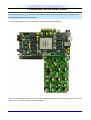
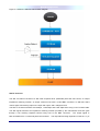
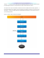
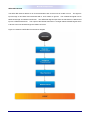
Terasic THDB-SUM
SDI HSMC
Terasic SDI HSMC Board
User Manual
Document Version 1.00
Document Version 1.00
AUG 21,
Aug. 20 2009 by Terasic
Introduction
Page Index
INTRODUCTION................................................................................................................................................................................. 1
1.1
1.1 FEATURES..................................................................................................................................................................... 1
1.2
1.2 ABOUT THE KIT ............................................................................................................................................................ 2
1.3
1.3 ASSEMBLE THE SDI HSMC BOARD ............................................................................................................................ 3
1.4
1.4 GETTING HELP ............................................................................................................................................................. 4
ARCHITECTURE ................................................................................................................................................................................ 5
2.1
2.1 LAYOUT AND COMPONETS............................................................................................................................................ 5
2.2
2.2 BLOCK DIAGRAM .......................................................................................................................................................... 7
BOARD COMPONENTS ................................................................................................................................................................... 8
3.1
3.1 THE SDI HSMC CONNECTOR ..................................................................................................................................... 8
3.2
3.2 AUDIO/VIDEO INPUT AND OUTPUT ............................................................................................................................. 16
3.3
3.3 CLOCK CIRCUITRY...................................................................................................................................................... 21
3.4
3.4 GENERAL USER INPUT/OUTPUT ................................................................................................................................ 24
3.5
3.5 POWER SUPPLY.......................................................................................................................................................... 25
DEMONSTRATION .......................................................................................................................................................................... 26
4.1
4.1 INTRODUCTION ........................................................................................................................................................... 26
4.2
4.2 SYSTEM REQUIREMENTS ........................................................................................................................................... 26
4.3
4.3 SETUP THE DEMONSTRATION .................................................................................................................................... 27
4.4
4.4 DEMO OPERATION ...................................................................................................................................................... 27
4.5
4.5 OVERVIEW .................................................................................................................................................................. 28
APPENDIX ......................................................................................................................................................................................... 30
5.1
5.1 REVISION HISTORY..................................................................................................................................................... 30
5.2
5.2 ALWAYS VISIT SDI HSMC W EBPAGE FOR NEW MAIN BOARD .................................................................................. 30
ii
Introduction
1
Introduction
The SDI HSMC Board is a transceiver serial digital interface HSMC board that provides a hardware platform
for developing video broadcasting systems. It is intended to be used by customers to implement and design
SDI and AES systems based on transceiver-based host boards with HSMC interface.
Furthermore, the SDI
HSMC board is designed for professional video equipment developers with SDI interface that allows FPGA
design to access to industry standard video transport signals.
1.1 1.1 Features
Figure 1.1 shows the photo of the SDI HSMC board. The important features are listed below:
•
•
•
•
SDI
Two SDI transmit (TX) channels with SDI cable tri-speed drivers
Two SDI receive (RX) channels with SDI cable equalizers
Two 75-Ω BNC SDI TX interfaces
Two 75-Ω BNC SDI RX interfaces
Adjustable 1.1 V to 1.8 V and Standard 3.3 V CMOS Input Signal Levels
AES3
Two RS422 transceivers for AES3 TX and AES3 RX channels
Two 75-Ω BNC AES3 RX interfaces
Two 75-Ω BNC AES3 TX interfaces
Power
High frequency switching regulator for 12-V to 5-V power conversion
Three linear regulators for 5-V to 3.3-V low noise power conversion
FDTIM analysis for power distribution network (PDN) decoupling
Clocks
One SDI multi-frequency VCXO femto clock video PLL
98.304 MHz/90.3168 MHz/122.88 MHz/112.896 MHz voltage-controlled crystal oscillator
(VCXO) based phase-locked loop (PLL)
One LVPECL differential clock buffer with two differential outputs – HSMC and SMA
•
Four digital audio isolation transformers
•
One multi-format video sync separator
•
One HSMC connector for interface conversion, which is fully compatible with HSMC host boards
1
Introduction
Figure 1.1. The SDI HSMC Board
1.2 1.2 About the KIT
This section describes the package content
•
SDI HSMC Board x 1
•
System CD-ROM x 1
The CD contains technical documents of the SDI HSMC, and one reference design along with the source
code.
Figure 1.2 SDI HSMC Package
2
Introduction
1.3 1.3 Assemble the SDI HSMC Board
This section describes how to connect the SDI HSMC board to a main board, and using the Stratix IV GX
FPGA Development Board as an example.
The SDI HSMC board connects to the Stratix IV GX FPGA Development Board.
Note.
Do not attempt to connect/remove the SDI HSMC daughter board to/from the main board when the
power is on, or else the hardware could be damaged.
3
Introduction
1.4 1.4 Getting Help
Here are some places to get help if you encounter any problem:
Email to [email protected]
Taiwan & China: +886-3-550-8800
Korea : +82-2-512-7661
Japan: +81-428-77-7000
4
Architecture
2
Architecture
This chapter covers the architecture of the SDI HSMC board including its PCB and block diagram.
2.1 2.1 Layout and Componets
The picture of the SDI HSMC board is shown in Figure 2.1 and Figure 2.2. It depicts the layout of the board and
indicates the location of the connectors and key components.
Figure 2.1. The SDI HSMC PCB and component diagram
5
Architecture
Figure 2.2. The SDI HSMC back side – HSMC connector view
The following components are provided on the SDI HSMC board :
•
SDI Output Channel 2 (J1), SDI Input Channel 2 (J2), AES Output Channel 1 (J3), Equalizer Bypass
Jumper (J5), Carrier Detect – Mute Jumper (J6), Equalizer Bypass Jumper (J7), SDI Output Channel 1
(J8), SDI Input Channel 1 (J9), AES Input Channel 1 (J10), SMA AES Clock Output (J12), AES Output
Channel 2 (J14), AES Input Channel 2 (J15), SMA SDI Clock Input (J16), SMA SDI Clock Output (N)
(J18)
•
SDI Cable Tri-speed Driver (U1), SDI Cable Tri-speed Driver (U2), AES VCXO PLL (U3), Mutli-format
Video Sync Separator (U4), High Frequency Switching Regulator (U5), SDI Multi-frequency VCXO
Femto Clock Video PLL (U6), LVPECL Differential Clock Buffer (U7), SDI Cable Equalizer (U8), RS422
Transceiver (U9), SDI Cable Equalizer (U10), Linear Regulator (U11), Linear Regulator (U12), Linear
Regulator (U13), Single Gate Tri-state Buffer (U14), Single Gate Tri-state Buffer (U15), RS422
Transceiver (U16), HSMC Connector (J19)
6
Architecture
2.2 2.2 Block Diagram
Figure 2.3 shows the block diagram of the SDI HSMC board
Figure 2.3. The block diagram of the SDI HSMC board
7
Board Components
3
Board Components
This section illustrates the detailed information of the components, connector interfaces, and the pin mapping
tables of the SDI HSMC board.
3.1 3.1 The SDI HSMC Connector
This section describes pin definition of the SDI HSMC interface onboard
All the control and data signals of the SDI and AES are connected to the HSMC connector, so users can fully
control the SDI HSMC board through the HSMC interface.
HSMC connector.
8
Power is derived from 3.3V and 12V of the
Board Components
Figure 3.1. The pin-outs of Bank 1 on the HSMC connector
9
Board Components
Figure 3.2. The pin-outs of Bank 2 of the HSMC connector.
10
Board Components
.
Figure 3.3. The pin-outs of Bank 3 of the HSMC connector
11
Board Components
The table 3.1 below lists the HSMC signal direction and description.
Table 3.1
Pin
Name
Direction
Description
1
N.C.
N/A
Not Connect
2
N.C.
N/A
Not Connect
3
N.C.
N/A
Not Connect
4
N.C.
N/A
Not Connect
5
N.C.
N/A
Not Connect
6
N.C.
N/A
Not Connect
7
N.C.
N/A
Not Connect
8
N.C.
N/A
Not Connect
9
N.C.
N/A
Not Connect
10
N.C.
N/A
Not Connect
11
N.C.
N/A
Not Connect
12
N.C.
N/A
Not Connect
13
N.C.
N/A
Not Connect
14
N.C.
N/A
Not Connect
15
N.C.
N/A
Not Connect
16
N.C.
N/A
Not Connect
17
N.C.
N/A
Not Connect
18
N.C.
N/A
Not Connect
19
N.C.
N/A
Not Connect
20
N.C.
N/A
Not Connect
21
N.C.
N/A
Not Connect
22
N.C.
N/A
Not Connect
23
N.C.
N/A
Not Connect
24
N.C.
N/A
Not Connect
25
SDI_TX_P2
Input
Differential transmitted data
26
SDI_EQOUT_P2
Output
Differential received data
27
SDI_TX_N2
Input
Differential transmitted data
28
SDI_EQOUT_N2
Output
Differential received data
29
SDI_TX_P1
Input
Differential transmitted data
30
SDI_EQOUT_P1
N/A
Differential received data
31
SDI_TX_N1
Input
Differential transmitted data
32
SDI_EQOUT_N1
Output
Differential received data
33
N.C.
N/A
Not Connect
Numbers
12
Board Components
34
N.C.
N/A
Not Connect
35
N.C.
N/A
Not Connect
36
N.C.
N/A
Not Connect
37
JTAG_TDO_TDI
Inout
JTAG data loop through
38
JTAG_TDO_TDI
Inout
JTAG data loop through
39
N.C.
N/A
Not Connect
40
N.C.
N/A
Not Connect
41
SDI_LED_TX_R1
Input
Red LED signal transmit channel 1
42
N.C.
N/A
Not Connect
43
SDI_LED_TX_R2
Input
Red LED signal transmit channel 2
44
N.C.
N/A
Not Connect
45
3V3
Power
Power 3.3V
46
12V
Power
Power 12V
47
SDI_LED_TX_G1
Input
Green LED signal transmit channel 1
48
N.C.
N/A
Not Connect
49
SDI_LED_TX_G2
Input
Green LED signal transmit channel 2
50
N.C.
N/A
Not Connect
51
3V3
Power
Power 3.3V
52
12V
Power
Power 12V
53
SDI_LED_RX_R2
Output
Red LED signal receive channel 2
54
N.C.
N/A
Not Connect
55
SDI_LED_RX_G2
Output
Green LED signal receive channel 2
56
N.C.
N/A
Not Connect
57
3V3
Power
Power 3.3V
58
12V
Power
Power 12V
59
SDI_LED_RX_R1
Output
Red LED signal receive channel 1
60
N.C.
N/A
Not Connect
61
SDI_LED_RX_G1
Output
Green LED signal receive channel 1
62
N.C.
N/A
Not Connect
63
3V3
Power
Power 3.3V
64
12V
Power
Power 12V
65
N.C.
N/A
Not Connect
66
N.C.
N/A
Not Connect
67
N.C.
N/A
Not Connect
68
N.C.
N/A
Not Connect
69
3V3
Power
Power 3.3V
70
12V
Power
Power 12V
71
SDI_RATE_SEL1
Input
Cable driver’s slew rate for desired bit rate
13
Board Components
72
N.C.
N/A
Not Connect
73
SDI_RATE_SEL2
Input
Cable driver’s slew rate for desired bit rate
74
N.C.
N/A
Not Connect
75
3V3
Power
Power 3.3V
76
12V
Power
Power 12V
77
EQ_BYPASS1
Input
Equalizer bypass receive channel 1
78
N.C.
N/A
Not Connect
79
EQ_BYPASS2
Input
Equalizer bypass receive channel 2
80
N.C.
N/A
Not Connect
81
3V3
Power
Power 3.3V
82
12V
Power
Power 12V
83
AES_CLK_S0
Input
AES frequency select
84
N.C.
N/A
Not Connect
85
AES_CLK_S1
Input
AES frequency select
86
N.C.
N/A
Not Connect
87
3V3
Power
Power 3.3V
88
12V
Power
Power 12V
89
AES_CLK_S2
Input
AES frequency select
90
N.C.
N/A
Not Connect
91
AES_CLK_PDTSn
Input
AES clock power down and tri-state
92
N.C.
N/A
Not Connect
93
3V3
Power
Power 3.3V
94
12V
Power
Power 12V
95
N.C.
N/A
Not Connect
96
AES_CLK
Output
AES clock reference
97
N.C.
N/A
Not Connect
98
N.C.
N/A
Not Connect
99
3V3
Power
Power 3.3V
100
12V
Power
Power 12V
101
AES_OUT1
Input
AES data output 1
102
AES_IN1
Input
AES data input 1
103
AES_OUT2
Input
AES data output 2
104
AES_IN2
Input
AES data input 2
105
3V3
Power
Power 3.3V
106
12V
Power
Power 12V
107
AES_VCXO_UP
Input
AES VCXO frequency control
108
N.C.
N/A
Not Connect
109
AES_VCXO_DN
Input
AES VCXO frequency control
14
Board Components
110
N.C.
N/A
Not Connect
111
3V3
Power
Power 3.3V
112
12V
Power
Power 12V
113
SDI_CLK_SEL
Input
SDI clock input select
114
N.C.
N/A
Not Connect
115
SDI_XTAL_SEL
Input
SDI clock crystal select
116
N.C.
N/A
Not Connect
117
3V3
Power
Power 3.3V
118
12V
Power
Power 12V
119
SDI_CLK_BP0
Input
SDI clock control
120
N.C.
N/A
Not Connect
121
SDI_CLK_BP1
Input
SDI clock control
122
N.C.
N/A
Not Connect
123
3V3
Power
Power 3.3V
124
12V
Power
Power 12V
125
N.C.
N/A
Not Connect
126
N.C.
N/A
Not Connect
127
SDI_CLK_N0
Input
SDI clock control
128
N.C.
N/A
Not Connect
129
3V3
Power
Power 3.3V
130
12V
Power
Power 12V
131
SDI_CLK_N1
Input
SDI clock control
132
N.C.
N/A
Not Connect
133
SDI_CLK_V0
Input
SDI clock control
134
N.C.
N/A
Not Connect
135
3V3
Power
Power 3.3V
136
12V
Power
Power 12V
137
SDI_CLK_V1
Input
SDI clock control
138
N.C.
N/A
Not Connect
139
SDI_CLK_V2
Input
SDI clock control
140
N.C.
N/A
Not Connect
141
3V3
Power
Power 3.3V
142
12V
Power
Power 12V
143
SDI_CLK_V3
Input
SDI clock control
144
ODDEVEN
Output
Video sync output of odd/even field
145
SDI_CLK_MLTF
Input
SDI clock control
146
VFORMAT
Output
Video sync output
147
3V3
Power
Power 3.3V
15
Board Components
148
12V
Power
Power 12V
149
SDI_CLK_RST
Input
SDI clock control
150
VSYNC
Output
Vertical sync output
151
SDI_CLK_OE
Input
SDI clock output enable
152
HSYNC
Output
Horizontal sync output
153
3V3
Power
Power 3.3V
154
12V
Power
Power 12V
155
SDI_HSMC_CLK
Input
SDI chip reference clock input
156
SDI_HSMC_CLK_P
Output
SDI clock hot reference clock
157
N.C.
N/A
Not Connect
158
SDI_HSMC_CLK_N
N/A
SDI clock hot reference clock
159
3V3
Power
Power 3.3V
160
GND
Power
Power Ground
3.2 3.2 Audio/Video Input and Output
This section describes the I/O channels of the SDI HSMC.
SDI RX Channels
The SDI RX channel consists of an SDI cable equalizer (LMH0344) with bypass, an input matching network,
an input vertical mount with a 4-GHz BNC connector, a bypass control signal, DC blocking caps on the input
and output, and a carrier detect LED.
The RX channel receives 270 Mbps, 1.485 Gbps, and 2.970 Gbps SDI signals through a single-ended 75-Ω
BNC connector.
The singles traverse an impedance-matching network provided by the manufacturer.
The
input signal is terminated to ground with a 75-Ω external resistor and is input into the SDI cable equalizer via a
1- µF DC blocking capacitor. The opposite leg of the SDI cable equalizer’s differential input pin is terminated
in the same way as the input signal and serves to correctly balance the input bias currents internal to the
equalizer.
The equalizer then equalizes the signal and outputs a 100-Ω differential signal to the SERDES
receiver located on the host HSMC device.
The differential output of the SDI cable equalizer passes through
1- µF DC blocking capacitors.
16
Board Components
Figure 3.4 shows the SDI RX channel block diagram
SDI TX Channels
The SDI TX channel consists of a SDI cable tri-speed driver (LMH0302) with slew rate control, an output
impedance matching network, an output vertical mount with a 4-GHz BNC connector, an SDI rate select
control signal, DC blocking caps on the input and output, and a red/green LED.
The SDI TX channel transmits at 270 Mbps, 1.485 Gbps and 2.970 Gbps rates using a 75-Ω coaxial cable.
The SDI signals traverses an impedance matching network provided by the manufacturer and then goes
through a DC blocking capacitor before being sent to the BNC connector.
The output signal is
back-terminated to 3.3 V externally with 75-Ω resistors. The output DC blocking capacitors consist of 4.7- µF
17
Board Components
capacitors.
The opposite leg of the SDI cable driver’s differential output pin is terminated in the same way as
the output signal and serves to correctly balance the output currents internal to the device.
The output of the TX pins of the HSMC host boards should not be installed with DC blocking capacitors.
If
DC blocking capacitors are installed, remove the capacitors and install 0-Ω resistors of the same foot print
size (0402).
The input of the SDI cable driver is differentially terminated with a 100-Ω resistor and has 4.7-
µF DC blocking capacitors.
Figure 3.5 shows the SDI TX Channel block diagram
18
Board Components
AES3 RX Channels
The AES3 RX channel delivers a 75-Ω load termination with a return loss of 25 dB or more. The signal is
input through a 75-Ω BNC and terminated with a 75-Ω resistor to ground.
The unbalanced signal is then
balanced through an isolation transformer. The differential signal output from the transformer is biased and
input to a RS422 transceiver.
The output of the RS422 transceiver is a single-ended LVCMOS signal which
is driven to the host board through the HSMC connector.
Figure 3.6 shows the AES3 RX Channel block diagram
19
Board Components
AES3 TX Channels
The AES3 TX channel is designed to have a balanced signal driver to the isolation transformer. The output
of the RS422 transceiver has an RX network to limit the output slew rate, thus limiting the bandwidth of AES3
output.
The AE3 channel is designed to support 192-kHz to 24-kHz sample rates.
The output is
unbalanced with a source impedance of 75 Ω and a return loss of 25 dB or more. The peak-to-peak output
voltage is 1.0V centered around the ground of the transmitter.
Figure 3.7 shows the AES3 TX Channel block diagram
20
Board Components
3.3 3.3 Clock Circuitry
This section describes the board’s clock inputs and outputs.
SDI Clock
The reference clocks can be generated from the host board, external video sources, and external SDI
sources. The output of the clock generator should produce frequency of 148.5 MHz or 148.5 MHz/1.001
(148.35 MHz) from the SMA outputs or the HSMC connector.
Figure 3.8 shows the SDI HSMC clocking diagram.
Figure 3.8 SDI HSMC Clocking diagram
The SDI multi-frequency VCXO femto clock video PLL (ICS810001-21) is utilized for the SDI reference clocks.
The board inputs two crystals, 27 MHz and 26.973027 MHz to the clock generator which allow low-jitter
operation for US and European SDI standard rates.
crystal is locked by the internal VCXO.
The HSMC signal SDI_XTAL_SEL determines which
Clock inputs to the SDI PLL can come from either the HSMC host or
through an SMA input where both inputs are end-terminated at 50 Ω to ground.
SDI_CLK_SEL determines which input is active.
21
The HSMC signal
Board Components
The output of the clock generator is single-ended.
A differential LVPECL clock buffer is used to convert the
reference clock to differential signal and drive the signal to the host device to prevent common mode noise
that might be present in the signaling path from the clock generator to the HSMC host device.
Host Board Reference Clock
You can select one of the several reference clock frequencies to input as a reference to the DI mult-frequency
VCXO femto clock video PLL.
For example, if the host board has a 100-MHz oscillator, you can divide the
frequency by 6,400 to 15.625 kHz and drive that frequency to the clock generator to be multiplied to 148.5
MHz. We recommend locking the VCXO PLL to a stable oscillator which is located on the host board when
the daughtercard is sourcing data or when the VCXO PLL is not locked onto a received signal or reference.
This locking prevents wandering or frequency hunting.
Loop Back Reference Clock From SDI Input
When an RX channel is locked onto the input data stream, the recovered clock represents the actual bit rate
of the stream. This recovered clock is often 74.25 MHz and can be buffered from the host board and driven
out through the HSMC interface to the clock generator on the SDI HSMC.
The clock output from the host is
cleaned (jitter), multiplied to 148.5 MHz, and driven back to the host board to be used as the SERDES
reference clock.
Using this technique maintains the flow through timing.
Studio Reference Timing
If a studio clock source (a 27-MHz source) is available, the source can be connected to the EXT CLK IN SMA
port on the daughtercard.
Studio Reference Video Timing
A video synchronizing separator is provided to synchronize the SDI video output streams to analog video.
The horizontal and vertical syncs are driven to the host board and can be driven back to the video clock
generator chip to produce a 148.5-MHz SERDES reference.
AES3 Clock
AES3 clocking uses clock device from IDT (ICS275-22) that comes with pre-programmed to produce 93.304
MHz, 90.3168 MHz (4x oversampling), 122.88 MHz, and 112.896 MHz (5x oversampling) from a 16.384-MHz
crystal.
Output CLK1 and CLK2 are connected to the HSMC and SMA connector respectively.
CLK1 is connected to the MSHC connector and drives a signal to the host device.
22
Output
Output CLK2 can be used
Board Components
for a reference, to trigger test equipment or to sync a signal to other devices in the AES3 system.
The base part (ICS275) is a VCXO that can have various combinations of input, output, and feedback dividers
to produce variations of the crystal frequency.
The control voltage input of the device is controlled by a
passive network of resistors and capacitors that are connected to tri-state buffers, one driven high and the
other driven low when in the active state (non-tri-stated).
The single gate devices are powered by 3.3 V to
allow full swing of the control voltage (Vin, AES_CLK_V) because the ICS275 is also powered by 3.3 V.
tri-state-enabled pins are controlled by the host device connected to the HSMC.
The
These pins should not be
allowed to float.
To use the ICS275 as a normally oscillator and not as a VCXO, drive signals AES_VCXO_UP and
AES_VCXO_DN both to logic 1.
Both output signals are enabled and the resulting voltage output after the
resistor or capacitor network is a mid-voltage driven to the Vin of the ICS275 device.
To use the ICS275 as a VCXO in a PLL application, connect the phase detector to the AES3 up and down
control signals.
Table 3.2 the audio rate and clock frequencies supported by the SDI HSMC
Audio Sample Rate (kHz)
Bit Rate Clock (MHz)
Oversampling Rate
VCXO Frequency
24.00
3.0720
32
98.3040
32.00
4.090
24
98.3040
44.10
5.6448
16
90.3168
48.00
6.1440
16
98.3040
88.20
11.2896
8
90.3168
96.00
12.2880
8
98.3040
176.4
22.5792
4
90.3168
192
24.5760
4
98.3040
24.00
3.0720
40
122.8800
32.00
4.0960
30
122.8800
44.10
5.6448
20
112.8960
48.00
6.1440
20
122.8800
88.20
11.2896
10
112.8960
96.00
12.2880
10
122.880
176.4
22.5792
5
112.8960
192
24.5760
5
122.8800
Table defines the frequency output with respect to the three 1-bit control signals, S [2:0].
and CLK4 are not used in the VCXO PLL.
Outputs from CLK3
The frequencies programmed into the VCXCO PLL support 4x
and 5x over-sampling of the most popular audio sample rates.
23
Board Components
Table 3.3 VCXO PLL Frequency Output
S2
S1
S0
CLK1 (MHz)
CLK2 (MHz)
CLK3
CLK4
0
0
0
98.304
98.304
OFF
OFF
0
0
1
90.3168
90.3168
OFF
OFF
0
1
0
122.88
122.88
OFF
OFF
0
1
1
112.896
112.896
OFF
OFF
1
0
0
98.304
122.88
OFF
OFF
1
0
1
90.3168
112.896
OFF
OFF
1
1
0
98.304
90.3168
OFF
OFF
1
1
1
122.88
112.896
OFF
OFF
3.4 3.4 General User Input/Output
This section describes the user I/O interface to the board
The SDI HSMC board has jumper switches CD_MUTE channels 1 and 2 and EQ_BYPASS channels 1 and 2.
By default, the jumpers are installed on the CD_MUTE jumper switches (J4 and J6), while the EQ_BYPASS
jumper switches (J5 and J7) are not installed.
Jumpers J5 (EQ_BYPASS2) and J7 (EQ_BYPASS1) can be
controlled from the host device.
Table 3.4 lists the jumper descriptions and schematic signal names
Board
Schematic
Reference
Signal Name
J4
CD_MUTE2
Description
Standard
Carrier detect jumper switch which connects to RX channel
2 (CD_MUTE2) on U8.
J5
EQ_BYPASS2
I/O
Signal short
This jumper is normally installed.
Equalizer bypass for RX channel 2.
The equalizer can be
CMOS
by passed manually when EQ_BYPASS2 signal is
tri-stated.
This jumper is normally not installed and the
switch is controlled by asserting the EQ_BYPASS2 signal.
A high signal bypasses the SDI receiver equalizer.
J6
CD_MUTE1
Carrier detect jumper switch which connects to RX channel
1 (CD_MUTE1) on U10.
Signal short
This jumper is normally
installed.
J7
EQ_BYPASS1
Equalizer bypass for RX channel 1.
The equalizer can be
bypassed manually when EQ_BYPASS1 signal is tri-stated
this jumper is normally not installed and the switch is
controlled by asserting the EQ_BYPASS1 signal.
signal bypasses the SDI receiver equalizer.
24
A high
CMOS
Board Components
3.5 3.5 Power Supply
This section describes the power supply on the SDI HSMC board
The power distribution on the SDI HSMC board is shown in Figure 3.9
Figure 3.9 Power distribution on the SDI HSMC board
25
Demonstration
4
Demonstration
This Chapter illustrates the reference design for the SDI HSMC board
4.1 4.1 Introduction
This section describes the functionality of the demonstration briefly.
The demonstration shows how to use the Stratix IV GX FPGA Development Board to test the functionality of
the SDI video and AES audio transmit and receive pairs.
The tests are PRBS data pattern loopback tests
using the two AES digital audio ports and the two SDI digital video ports on the SDI HSMC.
channel tests run at 24 Mbps and SDI tests run at 2.97 Gbps.
4.2 4.2 System Requirements
The following items are required for the SDI HSMC demonstration.
•
HSMC SDI Board x 1
•
Stratix IV GX FPGA Development Board x 1
•
75-Ω BNC to BNC Cables x 4
•
Jumpers for CD_MUTE x 2
26
AES audio
Demonstration
4.3 4.3 Setup the Demonstration
Figure 4.3 shows how to setup hardware for the SDI HSMC demonstration.
Note: The SDI HSMC board must be connected to HSMC Slot “A” of the Stratix IV GX FPGA Development
Board for this demonstration.
Figure 4.3
4.4 4.4 Demo Operation
This section describes the procedures of running the demonstration
FPGA Configuration
Demonstration Setup, File Locations, and Instructions
SDI HSMC Demo:
•
Project directory: S4PCIe_HSMCAESSDI_test
•
Bit Stream used: S4PCIe_HSMCAESSDI_test.sof
27
Demonstration
•
Connect the AES/SDI HSMC board to the Stratix IV GX FPGA Development Board to HSMC Slot “A”
•
Connect the 75-Ω BNC cables from:
J1 (SDI OUT 2) to J2 (SDI IN 2)
J8 (SDI OUT 1) to J9 (SDI IN 1)
J14 (AES OUT 2) to J2 (AES IN 2)
J3 (AES OUT 1) to J10 (AES IN 1)
•
Install Jumpers for J4 (CD_MUTE 2) and J6 (CD_MUTE 1)
•
Set the rotary switch (SW2) to the 1 position.
•
Power on the Stratix IV GX FPGA Development Board and download with SOF file
(S4PCIe_HSMCAESSDI_test.sof)
•
Press reset button located on the host board to initiate the test
4.5 4.5 Overview
This section describes the design concepts for the SDI HSMC demonstration.
To monitor the results of each test, connect a BNC loopback cable between the corresponding, transmit and
receive connectors.
Tests run on all channels simultaneously, but only channels with loopback cables
display accurate information.
When the Stratix IV GX FPGA Development Board is powered on, the LEDs (D1, D3, D5, D6) alternate
between the states of: OFF, RED, GREEN, ORANGE.
Connection Test:
The connection test verifies the connections made on the SDI and AES channels.
By pressing pushbutton PB0 on the host board it will check if everything is connected correctly and data is
being transmitted and received correctly.
The USER LEDs 1, 2, 4, 5 on the host board correspond to links
SDI port 1, SDI port2, AES port 1 and AES port2 respectively which will illuminate if the connection are
connected correctly.
If LEDs 1, 2, 4, 5 do not illuminate then there is connectivity issue with that link, otherwise if they all illuminate
then the receivers are receiving the correct data.
Error Insertion Test:
The error insertion test inserts a bit error into the transmit data stream each time you press the following push
button:
By pressing pushbutton PB1 which forces an error links on SDI and AES1 that causes LEDs 2 and 5 to go out
respectively.
By pressing pushbutton PB2 which forces an error links on SD2 and AES2 that causes LEDs 1 and 4 to go
out respectively.
28
Demonstration
By pressing PB0, LEDS 1, 2, 4, 5 will turn back on.
Self-debugging Test:
Perform the following test to debug connectivity issues with the SDI transmitters to SDI receivers, and AES
transmitters to AES receivers.
By disconnecting BNC from SDI OUT 1 (J8), LED 2 will go out.
By disconnecting BNC from SDI OUT 2 (J1), LED 1 will go out.
By disconnecting BNC from AES OUT 1 (J3), LED 5 will go out.
By disconnecting BNC from AES OUT 2 (J14), LED 4 will go out.
You may cross connect the SDI transmitters to the SDI receivers, as well as the AES transmitters to the AES
receivers.
If during a cross connection a channel fails, then the failure is in the transmitter of that channel
that was failing.
29
Appendix
5
Appendix
5.1 5.1 Revision History
Date
Change Log
AUG 20 , 2009
Initial Version
SEPT 23, 2009
SDI driver part number corrected in the SDI TX section
5.2 5.2 Always Visit SDI HSMC Webpage for New Main board
We will be continuing providing interesting examples and labs on our SDI HSMC
webpage. Please visit www.altera.com or hsmcsdi.terasic.com for more information.
30