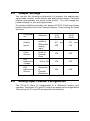
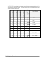
1
NuDAQ / NuIPC 9112 Series Multi-function DAS Cards for PCI / 3U CompactPCI User’s Manual Copyright ©1996~2000 ADLINK Technology Inc. ALL RIGHTS RESERVED. Manual Rev 3.50: May 25, 2000 The information in this document is subject to change without prior notice in order to improve reliability, design and function and does not represent a commitment on the part of the manufacturer. In no event will the manufacturer be liable for direct, indirect, special, incidental, or consequential damages arising out of the use or inability to use the product or documentation, even if advised of the possibility of such damages. This document contains proprietary information protected by copyright. All rights are reserved. No part of this manual may be reproduced by any mechanical, electronic, or other means in any form without prior written permission of the manufacturer. Trademarks NuDAQ , NuIPC are registered trademarks of ADLINK Technology Inc. Other products names mentioned herein are used for identification purposes only and may be trademarks and/or registered trademarks of their respective companies. Getting service from ADLINK Customer Satisfaction is always the most important thing for ADLINK Tech Inc. If you need any help or service, please contact us and get it. ADLINK Technology Inc. Web Site http://www.adlink.com.tw Sales & Service [email protected] Technical NuDAQ [email protected] Support NuDAM [email protected] NuIPC [email protected] NuPRO [email protected] Software [email protected] AMB [email protected] TEL +886-2-82265877 FAX +886-2-82265717 Address 9F, No. 166, Jian Yi Road, Chungho City, Taipei, 235 Taiwan, R.O.C. Please inform or FAX us of your detailed information for a prompt, satisfactory and constant service. Detailed Company Information Company/Organization Contact Person E-mail Address Address Country TEL FAX Web Site Questions Product Model Environment to Use OS Computer Brand M/B : CPU : Chipset : Bios : Video Card : Network Interface Card : Other : Challenge Description Suggestions for ADLink CONTENTS Chapter 1 Introduction ........................................... 1 1.1 1.2 1.3 1.4 Features............................................................................... 1 Applications......................................................................... 2 Specifications ...................................................................... 2 Software Supporting............................................................ 4 1.4.1 1.4.2 1.4.3 1.4.4 1.4.5 1.4.6 1.4.7 1.4.8 1.4.9 Programming Library ........................................................................... 4 ® PCIS-LVIEW: LabVIEW Driver.......................................................... 4 PCIS-VEE: HP-VEE Driver................................................................... 5 DAQBenchTM: ActiveX Controls ........................................................ 5 DASYLabTM PRO .................................................................................... 5 PCIS-DDE: DDE Server and InTouchTM........................................... 5 PCIS-ISG: ISaGRAFT M driver............................................................... 5 PCIS-ICL: InControlT M Driver .............................................................. 5 PCIS-OPC: OPC Server........................................................................ 5 Chapter 2 Installation............................................. 6 2.1 2.2 2.3 2.4 2.5 2.6 2.7 2.8 2.9 What You Have .................................................................... 6 Unpacking............................................................................ 7 Device Installation for Windows Systems............................ 7 PCB Layout.......................................................................... 8 Jumper Settings .................................................................10 Analog Input Channel Configuration ..................................10 Clock Source Setting ..........................................................11 D/A Reference Voltage Setting............................................11 Connectors Pin Assignments.............................................13 2.9.1 2.9.2 Pin Assignments of PCI-9112...........................................................13 Pin Assignments of cPCI-9112 ........................................................15 2.10 Hardware Installation Outline .............................................16 2.11 Device Installation for Windows Systems...........................16 2.12 Daughter Board Connection ...............................................17 2.12.1 2.12.2 2.12.3 2.12.4 2.12.5 Connect with ACLD-8125 ..................................................................17 Connect with ACLD-9137 ..................................................................17 Connect with ACLD-9182 ..................................................................17 Connect with ACLD-9185 ..................................................................18 Connect with ACLD-9138 and ACLD-9188....................................18 Chapter 3 Registers Format.................................19 3.1 3.2 3.3 I/O Registers Map ...............................................................19 A/D Data Registers..............................................................20 D/A Output Register............................................................21 Contents • i 3.4 3.5 3.6 3.7 3.8 3.9 3.10 A/D control Register ...........................................................22 A/D Status Register ............................................................25 Software Trigger Register...................................................25 Digital I/O register...............................................................26 Internal Timer/Counter Register..........................................27 High Level Programming....................................................27 Low Level Programming.....................................................27 Chapter 4 Operation Theorem.............................28 4.1 4.2 A/D Conversion...................................................................28 Analog Input Signal Connection .........................................28 4.2.1 4.2.2 4.2.3 4.3 4.4 4.5 A/D Conversion Procedure...............................................................31 A/D Trigger Modes ..............................................................................31 A/D Data Transfer Modes..................................................................32 D/A Conversion...................................................................33 Digital Input and Output......................................................34 Timer/Counter Operation ....................................................35 Chapter 5 C/C++ Library .......................................39 5.1 5.2 Libraries Installation...........................................................39 Programming Guide............................................................40 5.2.1 5.2.2 5.3 5.4 5.5 5.6 5.7 5.8 5.9 5.10 5.11 5.12 5.13 5.14 5.15 5.16 5.17 5.18 5.19 5.20 Naming Convention ............................................................................40 Data Types.............................................................................................40 _9112_Initial........................................................................41 _9112_DI .............................................................................42 _9112_DI _Channel .............................................................42 _9112_DO ...........................................................................43 _9112_DA............................................................................44 _9112_AD_Set_Channel......................................................45 _9112_AD_Set_Range.........................................................46 _9112_AD_Set_Mode ..........................................................47 _9112_AD_Set_Autoscan....................................................48 _9112_AD_Soft_Trig ...........................................................49 _9112_AD_Aquire ...............................................................50 _9112_AD_DMA_Start .........................................................51 _9112_AD_DMA_Status ......................................................53 _9112_AD_DMA_Stop.........................................................54 _9112_ContDmaStart ..........................................................55 _9112_CheckHalfReady ......................................................56 _9112_DblBufferTransfer....................................................57 _9112_GetOverrunStatus....................................................57 ii• Contents 5.21 5.22 5.23 5.24 5.25 5.26 5.27 5.28 5.29 5.30 5.32 _9112_ContDmaStop ..........................................................58 _9112_AD_INT_Start ...........................................................59 _9112_AD_INT_Status ........................................................60 _9112_AD_INT_Stop ...........................................................61 _9112_AD_Timer.................................................................61 _9112_TIMER_Start.............................................................63 _9112_TIMER_Read ............................................................63 _9112_TIMER_Stop .............................................................64 _9112_Alloc_DMA_Mem .....................................................64 _9112_Free_DMA_Mem.......................................................65 _9112_Get_Sample .............................................................65 Chapter 6 Calibration............................................67 6.1 6.2 6.3 What do you need...............................................................67 VR Assignment ...................................................................68 A/D Adjustment...................................................................68 6.3.1 6.3.2 6.4 Bipolar Calibration ..............................................................................68 Unipolar Calibration............................................................................68 D/A Adjustment...................................................................69 6.4.1 6.4.2 Reference Voltage Calibration .........................................................69 D/A Channel Calibration ....................................................................69 Chapter 7 Software Utilities ................................70 7.1 Software Utility ...................................................................70 7.1.1 7.1.2 7.1.3 7.1.4 7.2 Running the Utility ..............................................................................71 System Configuration ........................................................................71 Calibration .............................................................................................71 Functional Testing ..............................................................................72 PCI SCAN Utility .................................................................72 Appendix A. Demo. Programs ..............................73 Product Warranty/Service ....................................75 Contents • iii How to Use This Guide This manual is for helping users to manipulate the PCI-9112 and cPCI9112. The functionality of PCI-9112 and cPCI-9112 are the same. Therefore, the “PCI-9112” in this manual represent both the PCI-9112 and cPCI-9112 without specifications. The manual describes how to modify various settings on the PCI-9112 card to meet your requirements. It is divided into seven chapters: Ø Ø Ø Ø Ø Ø Ø Chapter 1, Introduction, gives an overview of the product features, applications, and specifications. Chapter 2, Installation, describes how to install the PCI-9112. The layout of PCI-9112 is shown, jumper setting for analog input channel configuration, D/A reference voltage settings are specified. The connectors' pin assignment and how to connect the outside signal and devices are also described. Chapter 3, Registers Format, describes the details of register format and structure of the PCI-9112, this information is very important for the programmers who want to control the hardware by low-level programming. Chapter 4, Operation Theorem, describes how to operate the PCI-9112. The A/D, D/A, DIO and timer/counter functions are introduced. Some programming concepts are also specified. Chapter 5, C/C++ Library, describes the software utility and library of PCI-9112, and also describes how to install and operate the utility and library to meet your requirements and help you to program your own software application. Chapter 6, Calibration, describes how to calibrate the PCI-9112 for accurate measurement. Chapter 7, Software Utility, describes the software utilities which can help you to run the card. 1 Introduction The 9112 series products are multi-function data acquisition cards.. The 9112 series includes: PCI-9112: 12-bit 100KHz Multifunction DAS card cPCI-9112: 12-bit 100KHz Multifunction DAS card for 3U ComptactPCI The 9112 series DAS cards are using state-of-the-art technology to make this card ideal for data logging and signal analysis applications in medical, process control, etc. 1.1 Features The PCI-9112 PCI Bus Advanced Data Acquisition Card provides the following advanced features: Ø Ø Ø Ø Ø Ø Ø Ø Ø Ø Ø Ø Ø Ø Ø 32-bit PCI-Bus 12-bit analog input resolution On-board A/D FIFO memory Auto-scanning channel selection Up to 110Khz A/D sampling rates 16 single-ended or 8 differential analog input channels Bipolar or unipolar input signals Programmable gain of x0.5, x1, x2, x4, x8 On-chip sample & hold Two 12-bit monolithic multiplying analog output channels 16 digital output channels 16 digital input channels 3 independent programmable 16-bit down counters Three A/D trigger modes : software trigger, programmable pacer trigger, and external pulse trigger. Integral DC-to-DC converter for stable analog power source Introduction • 1 Ø Ø Ø 1.2 Applications Ø Ø Ø Ø Ø Ø Ø Ø Ø 1.3 u u 37-pin D-type connector for PCI-9112 100-pin SCSI-type connector for cPCI-9112 Half-size PCB Industrial and laboratory ON/OFF control Energy management Annunciation 16 TTL/DTL compatible digital input channels Security controller Product test Event and frequency counting Waveform and pulse generation BCD interface driver Specifications Analog Input (A/D) Converter: ADS774 or equivalent, successive approximation type Resolution: 12-bit Numbers of Input Channel: 16 single-ended or 8 differential Input Range: (Programmable) Bipolar : ± 10V, ± 5V, ± 2.5V, ± 1.25V, ± 0.625V Unipolar : 0~10V, 0~5V, 0~2.5V, 0~1.25V Conversion Time: 8 µ sec Throughput: 110KHz multiplexing (maximum) Analog Input Over-voltage Protection: Continuous ± 35V max. Accuracy: GAIN = 0.5, 1 0.01% of FSR ±1 LSB GAIN = 2, 4 0.02% of FSR ±1 LSB GAIN = 8 0.04% of FSR ±1 LSB Ø Input Impedance: 10 MΩ Ø Trigger Modes: Software, Timer Pacer, and External trigger Ø Data Transfer Modes: Bus mastering DMA, Program control, Interrupt Ø FIFO Depth: 8 words for PCI-9112, 2K words for cPCI-9112 only Ø Ø Ø Ø Ø Ø Ø Ø Ø Ø Ø Ø Ø Ø Analog Output (D/A) Numbers of Output Channel: 2 double-buffered analog output Resolution: 12-bit Output Range: Internal Reference: (unipolar) 0~5V or 0~10V 2 • Introduction u u u Ø Ø Ø Ø Ø External Reference: (unipolar) max. +10V or -10V Converter: DAC7541 or equivalent, monolithic multiplying Settling Time: 30 µ sec Linearity: ±1/2 bit LSB Output Driving Capability: ±5mA max. Ø Ø Ø Ø Ø Ø Ø Ø Ø Ø Ø Ø Ø Digital I/O (DIO) Numbers of channels: 16 TTL compatible inputs and outputs Input Voltage: Low: Min. 0V. Max. 0.8V High: Min. +2.0V Input Load: Low: +0.5V @ -0.2mA max. High: +2.7V @+20mA max. Output Voltage: Low: Min. 0V; Max. 0.4V High: Min. +2.4V Driving Capacity: Low: Max. +0.5V at 8.0mA (Sink) High: Min. +2.7V at 0.4mA (Source) Programmable Counter Timer / Counter Device: 8254 A/D pacer timer: 32-bit timer (two 16-bit counter cascaded together) with a 2MHz time base Ø Pacer Frequency Range: 0.00046 Hz ~ 100K Hz Ø Counter: One 16-bit counter with a 2MHz time base Ø Ø Ø Ø Ø Ø Ø Ø Ø Ø Ø Ø Ø Ø Ø Ø General Specifications Connector : 37-pin D-type connector Operating Temperature: 0° C ~ 60° C Storage Temperature: -20° C ~ 80° C Humidity: 5 ~ 95%, non-condensing Power Consumption: PCI-9112: +5 V @ 460 mA typical +12V @ 110 mA typical cPCI-9112: +5 V @ 600 mA typical +12V @ 20 mA typical PCB Dimension: PCI-9112: Compact size only 102mm(H) X 173mm(L) cPCI-9112: Standard CompactPCI form factor Introduction • 3 1.4 Software Supporting ADLink provides versatile software drivers and packages for users’ different approach to built-up a system. We not only provide programming library such as DLL for many Windows systems, but also ® provide drivers for many software package such as LabVIEW , HP TM TM TM TM TM VEE , DASYLab , InTouch , InControl , ISaGRAF , and so on. All the software options are included in the ADLink CD. The non-free software drivers are protected with serial licensed code. Without the software serial number, you can still install them and run the demo version for two hours for demonstration purpose. Please contact with your dealer to purchase the formal license serial code. 1.4.1 Programming Library For customers who are writing their own programs, we provide function libraries for m any different operating systems, including: u DOS Library: Borland C/C++ and Microsoft C++, the functions descriptions are included in this user’s guide. u Windows 95 DLL: For VB, VC++, Delphi, BC5, the functions descriptions are included in this user’s guide. u PCIS-DASK: Include device drivers and DLL for Windows 98, Windows NT and Windows 2000. DLL is binary compatible across Windows 98, Windows NT and Windows 2000. That means all applications developed with PCIS-DASK are compatible across Windows 98, Windows NT and Windows 2000. The developing environment can be VB, VC++, Delphi, BC5, or any Windows programming language that allows calls to a DLL. The user’s guide and function reference manual of PCISDASK are in the CD. Please refer the PDF manual files under \\Manual_PDF\Software\PCIS-DASK The above software drivers are shipped with the board. Please refer to the “Software Installation Guide” to install these drivers. 1.4.2 ® PCIS-LVIEW: LabVIEW Driver PCIS-LVIEW contains the VIs, which are used to interface with NI’s ® LabVIEW software package. The PCIS-LVIEW supports Windows ® 95/98/NT/2000. The LabVIEW drivers are free shipped with the board. You can install and use them without license. For detail information about PCIS-LVIEW, please refer to the user’s guide in the CD. (\\Manual_PDF\Software\PCIS-LVIEW) 4 • Introduction 1.4.3 PCIS-VEE: HP-VEE Driver The PCIS-VEE includes the user objects, which are used to interface with HP VEE software package. PCIS-VEE supports Windows 95/98/NT. The HP-VEE drivers are free shipped with the board. You can install and use them without license. For detail information about PCIS-VEE, please refer to the user’s guide in the CD. (\\Manual_PDF\Software\PCIS-VEE) 1.4.4 TM DAQBench : ActiveX Controls We suggest the customers who are familiar with ActiveX controls and VB/VC++ programming use the DAQBenchTM ActiveX Control components library for developing applications. The DAQBenchTM is designed under Windows NT/98. For more detailed information about DAQBench, please refer to the user’s guide in the CD. (\\Manual_PDF\Software\DAQBench\DAQBench Manual.PDF) 1.4.5 TM DASYLab PRO DASYLab is an easy-to-use software package, which provides easy-setup instrument functions such as FFT analysis. Please contact us to get DASYLab PRO, which include DASYLab and ADLink hardware drivers. 1.4.6 TM PCIS-DDE: DDE Server and InTouch DDE stands for Dynamic Data Exchange specifications. The PCIS-DDE includes the PCI cards’ DDE server. The PCIS-DDE server is included in the ADLINK CD. It needs license. The DDE server can be used conjunction with any DDE client under Windows NT. 1.4.7 PCIS-ISG: ISaGRAF TM driver The ISaGRAF WorkBench is an IEC1131-3 SoftPLC control program development environment. The PCIS-ISG includes ADLink products’ target drivers for ISaGRAF under Windows NT environment. The PCISISG is included in the ADLINK CD. It needs license. 1.4.8 TM PCIS-ICL: InControl Driver PCIS-ICL is the InControl driver which support the Windows NT. The PCIS-ICL is included in the ADLINK CD. It needs license. 1.4.9 PCIS-OPC: OPC Server PCIS-OPC is an OPC Server, which can link with the OPC clients. There are many software packages on the market can provide the OPC clients now. The PCIS-OPC supports the Windows NT. It needs license. Introduction • 5 2 Installation This chapter describes how to install the 9112 series cards. Please follow the follow steps to install. u Check what you have (section 2.1) u Unpacking (section 2.2) u Check the PCB and jumper location(section 2.3) u Setup jumpers (section 2.4~2.8) u Install the hardware and setup and jumpers (section 2.10) u Install the software drivers and run utility to test (section 2.11) u Cabling with external devices (section 2.9 and 2.12) 2.1 What You Have In addition to this User's Guide, the package includes the following items: Ø Ø Ø PCI-9112 or cPCI-9112 Enhanced Multi-function DAS Card ADLINK Software CD Software Installation Guide If any of these items is missing or damaged, contact the dealer from whom you purchased the product. Save the shipping materials and carton in case you want to ship or store the product in the future. 6 • Installation 2.2 Unpacking The card contains sensitive electronic components that can be easily damaged by static electricity. Failure to perform the procedure outlined below may damage the on board devices. The board is packaged in an anti-static bag to avoid damage to the sensitive IC on the board. After opening the card module carton, extract the bag and place it only on a grounded anti-static surface to establish grounding. The card should be handled on a grounded anti-static mat. The operator should be wearing an anti-static wristband, grounded at the same point as the anti -static mat. Inspect the card for obvious damage. Shipping and handling may cause damage to your module. Be sure there are no shipping and handing damages on the module before processing. Note : DO NOT ATTEMPT TO INSTALL A DAMAGED BOARD IN THE COMPUTER. You are now ready to install your card. 2.3 Device Installation for Windows Systems Once Windows 95/98/2000 has started, the Plug and Play function of Windows system will find the new NuDAQ/NuIPC cards. If this is the first time to install NuDAQ/NuIPC cards in your Windows system , you will be informed to input the device information source. Please refer to the “Software Installation Guide” for the steps of installing the device. Installation • 7 8 • Installation JP 4 EXTREF DIFF INTREF SING -5V -10V CN3 JP 3 JP 5 VR7 VR5 VR3 VR6 VR4 VR2 ADS-774 ALTERA PCI -Bus Controller DC-DC Converter DIFF INTCLK JP 2 SING EXTCLK .. .. . . .. .. .. .. .. .. .. .. .. .. .. .. .. .. .. CN2 .. .. . . .. .. .. CN1 PCI-9112 Multi-function DA&C JP 1 2.4 PCB Layout PCI-9112 Layout Figure 2.1 PCB Layout of the PCI-9112 cPCI-9112 Layout Figure 2.2 PCB Layout of the PCI-9112 Installation • 9 2.5 Jumper Settings You can set the following configuration by jumpers: the analog input signal mode, counter’s clock source, and analog output range. The card's jumpers and switches are preset at the factory. You can change the jumper settings for your own applications. For system reliability and safety, the design of PCI-9112 still keeps some board configurations to be set through jumpers. These setting are listed as below. Configurat ion Attributes Singleended or Differential Analog Input Internal Clock or External Clock Analog Inputs Clock Source D/A Reference Voltage -10V or -5V Jumpers (PCI9112) Jumpers (cPCI9112) JP1 JP5 JP1 JP4 and JP2 JP2 JP3 JP3 Internal Reference JP4 or External Reference Table 2.1 Jumpers Listing Table D/A Reference Source 2.6 and JP5 Analog Input Channel Configuration The PCI-9112 offers 16 single-ended or 8 differential analog input channels. The jumper JP1 and JP5 control the analog input configurations. The settings of JP1 and JP5 are specified as following: 10 • Installation PCI-9112 cPCI-9112 SINGLE Single-ended JP5 SINGLE SINGLE JP1 JP4 SINGLE JP1 (default setting) Differential Input DIFF DIFF DIFF DIFF SINGLE SINGLE SINGLE SINGLE JP5 JP1 DIFF DIFF Figure 2.2 2.7 JP4 JP1 DIFF DIFF Analog Input Mode Setting Clock Source Setting The programmable interval timer 8254 is used in the PCI-9112. It provides 3 independent 16-bit programmable down counters. The input of counter 2 is connected to a precision 2MHz oscillator for internal pacer. The input of counter 1 is cascaded from the output of counter 2. The channel 0 is free for user's applications. There are two selections for the clock source of channel 0 : the internal 2MHz clock or the external clock signal from connector CN3 pin 35. The setting of clock is shown as Figure 2.3. Internal Clock Source: 2MHz (default setting) External Clock Source INTCLK JP2 EXTCLK INTCLK JP2 EXTCLK Figure 2.3 Timer's Clock Source Setting 2.8 D/A Reference Voltage Setting The D/A converter's reference voltage source can be supplied both internally and external. The external reference voltage comes from connector CN3 pin 31 (ExtRef1) and pin12 (ExtRef2), see section 3.1. The reference source of D/A channel 1 and channel 2 are selected by JP4, respectively. Their possible settings are shown as below: Installation • 11 JP4(PCI-9112) JP5(cPCI-9112) D/A CH1 is External D/A CH2 is External D/A CH1 is External D/A CH2 is Internal D/A CH1 is Internal D/A CH2 is External D/A CH1 is Internal D/A CH2 is Internal (default setting) INTREF INTREF ExtRef1 ExtRef2 INTREF INTREF ExtRef1 ExtRef2 INTREF INTREF ExtRef1 ExtRef2 INTREF INTREF ExtRef1 ExtRef2 Figure 2.4 Analog Output Voltage Setting The internal A/D reference voltage can be set to –5V or –10V by JP3. The possible configurations are specified as Figure 2.5. Note that the internal reference voltage is used only when the JP4 is set to internal reference only. Reference Voltage is -5V (default setting) Reference Voltage is -10V -10V JP3 -5V -10V JP3 -5V Figure 2.5 Internal Reference Voltage Setting Note : If the -10V D/A reference voltage is selected, the D/A output range is 0V~10V. On the other hand, if the -5V is selected, the D/A output range is 0V~5V. 12 • Installation 2.9 Connectors Pin Assignments 2.9.1 Pin Assignments of PCI-9112 The PCI-9112 comes equipped with two 20-pin insulation displacement connectors - CN1 and CN2 and one 37-pin D-type connector - CN3. The CN1 and CN2 are located on board and CN3 located at the rear plate. CN1 is for digital signal input, CN2 for digital signal output, CN3 for analog input, analog output and timer/counter's signals. The pin assignments for each connector are illustrated in the Figure 2.9.1~ Figure 2.9.3. CN 3: Analog Input / Output & Counter/Timer (for single-ended connection) (for differential connection) CN3 AI0 AI1 AI2 AI3 AI4 AI5 AI6 AI7 A.GND A.GND V.REF ExtRef2 +12V A.GND D.GND COUT0 ExtTrg N/C +5V 1 2 3 4 5 6 7 8 9 10 11 12 13 14 15 16 17 18 19 20 21 22 23 24 25 26 27 28 29 30 31 32 33 34 35 36 37 AI8 AI9 AI10 AI11 AI12 AI13 AI14 AI15 A.GND A.GND AO1 ExtRef1 AO2 GATE0 GATE COUT1 N/C ExtCLK Figure 2.9.1 Pin Assignments of CN3 Legend : AIn AIHn AILn ExtRef n AOn ExtCLK ExtTrig CLK : Analog Input Channel n ( single-ended) : Analog High Input Channel n ( differential) : Analog Low Input Channel n ( differential) : External Reference Voltage for D/A CH n : Analog Output Channel n : External Clock Input : External Trigger Signal : Clock input for 8254 Installation • 13 GATE COUT n V.ERF A.GND GND : Gate input for 8254 : Signal output of Counter n : Voltage Reference : Analog Ground : Ground CN 1: Digital Signal Input (DI 0 - 15) CN1 DI 1 1 2 DI 3 3 4 DI 5 5 6 DI 7 7 8 DI 9 9 10 DI 11 11 12 DI 13 13 14 DI 15 15 16 GND 17 18 +12V 19 20 Figure 2.9.2 Pin Assignment of CN1 DI 0 DI 2 DI 4 DI 6 DI 8 DI 10 DI 12 DI 14 GND +5V CN 2: Digital Signal Output (DO 0 - 15) CN2 DO 1 DO 0 1 2 DO 3 DO 2 3 4 DO 5 DO 4 5 6 DO 7 DO 6 7 8 DO 9 DO 8 9 10 DO 11 DO 10 11 12 DO 13 DO 12 13 14 DO 15 DO 14 15 16 GND GND 17 18 +12V +5V 19 20 Figure 2.9.3 Pin Assignment of CN2 Legend : DO n DI n GND 14 • Installation : Digital output signal channel n : Digital input signal channel n : Digital ground 2.9.2 Pin Assignments of cPCI-9112 (1) (2) (3) (48) (49) (50) Legend : AINm AINHm AINLm ExtTrig DIN_x DOUT_x ExtCLK COUT n GATE0 GATE ExtRef n DAn REFout 5Vout 12Vout A.GND GND (51) (52) (53) (98) (99) (100) (1) DOUT_0 (26) DIN_9 GND (76) GND (2) DOUT_1 (27) DIN_10 GND (77) GND (3) DOUT_2 (28) DIN_11 GND (78) GND (4) DOUT_3 (29) DIN_12 GND (79) GND (5) DOUT_4 (30) DIN_13 GND (80) GND (6) DOUT_5 (31) DIN_14 GND (81) 5Vout (7) DOUT_6 (32) DIN_15 GND (82) 5Vout (8) DOUT_7 (33) EXTCLK GND (83) GND (9) DOUT_8 (34) EXTTRG GND (84) GND (10) DOUT_9 (35) COUT0 GND (85) COUT1 (11) DOUT_10 (36) (61) GND (86) GATE (12) DOUT_11 (37) (62) GND (87) AGND (13) DOUT_12 (38) (51) (52) (53) (54) (55) (56) (57) (58) (59) (60) GATE0 12VOUT ExtVref2 : Analog Input Channel m ( single-ended) : Analog High Input Channel m ( differential) : Analog Low Input Channel m ( differential) : External AD Trigger Signal : Digital Input Channel x : Digital Output Channel x : External Clock Input for 8254 Counter #0 : Signal output of Counter n : Gate input for 8254 Timer #0 : Gate input for 8254 Timer #1,2 : External Reference Voltage for D/A CH n : Analog Output Channel n (n=1,2) : Internal Voltage Reference Output : Internal 5V Output : Internal 12V Output : Analog Ground : Ground Installation • 15 2.10 Hardware Installation Outline PCI configuration The PCI cards (or CompactPCI cards) are equipped with plug and play PCI controller, it can request base addresses and interrupt according to PCI standard. The system BIOS will install the system resource based on the PCI cards’ configuration registers and system parameters (which are set by system BIOS). Interrupt assignment and memory usage (I/O port locations) of the PCI cards can be assigned by system BIOS only. These system resource assignments are done on a board-by-board basis. It is not suggested to assign the system resource by any other methods. PCI slot selection The PCI card can be inserted to any PCI slot without any configuration for system resource. Please note that the PCI system board and slot must provide bus-mastering capability to operate this board well. Installation Procedures 1.Turn off your computer. 2.Turn off all accessories (printer, modem, monitor, etc.) connected to your computer. 3. Remove the cover from your computer. 4. Setup jumpers on the PCI or CompactPCI card. 5. Select a 32-bit PCI slot. PCI slot are short than ISA or EISA slots, and are usually white or ivory. 6.Before handling the PCI cards, discharge any static buildup on your body by touching the metal case of the computer. Hold the edge and do not touch the components. 7.Position the board into the PCI slot you selected. 8.Secure the card in place at the rear panel of the system. 2.11 Device Installation for Windows Systems Once Windows 95/98/2000 has started, the Plug and Play function of Windows system will find the new NuDAQ/NuIPC cards. If this is the first time to install NuDAQ/NuIPC cards in your Windows system , you will be informed to input the device information source. Please refer to the “Software Installation Guide” for the steps of installing the device. . 16 • Installation 2.12 Daughter Board Connection The PCI-9112 can be connected with five different daughter boards, ACLD-8125, 9137, 9138, 9182, 9185, and 9188. The functionality and connections are specified in the following sections. The cPCI-9112 is equipped with 100 pin SCSI-II type connector, the DIN100S is a general purpose terminal board for connecting the external devices. 2.12.1 Connect with ACLD-8125 The ACLD-8125 has a 37-pin D-sub connector, which can connect with PCI-9112 through 37-pin assemble cable. The most outstanding feature of this daughter board is a CJC (cold junction compensation) circuit on board. You can directly connect the thermocouple on the ACL-8125 board. The CJC only suitable for High Gain version board. 2.12.2 Connect with ACLD-9137 The ACLD-9137 is a direct connector for the card which is equipped with 37-pin D-sub connector. This board provides a simple way for connection. It is very suitable for the simple applications that do not need complex signal condition before the A/D conversion is performed. 2.12.3 Connect with ACLD-9182 The ACLD-9182 is a 16 channel isolated digital input board. This board is connected with CN1 of PCI-9112 via 20-pin flat cable. The advantage of board is a 500Vdc isolation voltage is provided, and it can protect your PC ACLD9185 CN2 CN1 ACLDPCI 9182 when an abnormal input signal - is occurred. system from damage Installation • 17 2.12.4 Connect with ACLD-9185 The ACLD-9185 is a 16 channel SPDT relay output board. This board is connected with CN2 of PCI-9112 via 20-pin flat cable. by using this board, you can control outside device through the digital output signals. 2.12.5 Connect with ACLD-9138 and ACLD-9188 ACLD-9138 and ACLD-9188 are general purpose terminal boards for all the card which comes equipped with 37-pin D-sub connector. The ACLD9138 has a LED indicator to show the power ON/OFF of your computer system. CN1 CN3 CN2 ACLD-9188 PCI-9112 18 • Installation 3 Registers Format The detailed descriptions of the register format and structure of the PCI9112 are specified in this chapter. This information is quite useful for the programmer who wish to handle the card by low-level program. In addition, the low level programming syntax is introduced. This information can help the beginners to operate the PCI-9112 in the shortest learning time. 3.1 I/O Registers Map The PCI-9112 functions as 32-bit PCI target device to any master on the PCI bus. It supports burst transfer to memory space by using 32-bit data. All data read and write will base on 32-bit data.There are three types of registers on the PCI-6308: PCI Configuration Registers (PCR), Local Configuration Registers (LCR) and 9112 registers. The PCR, which compliant to the PCI-bus specifications, is initialized and controlled by the plug & play (PnP) PCI BIOS. User‘s can study the PCI BIOS specification to understand the operation of the PCR. Please contact with PCISIG to acquire the specifications of the PCI interface. The LCR is specified by the PCI bus controller AMCC-5933, which is provided by AMCC Corp. (www. amcc .com) It is not necessary for users to understand the details of the LCR if you use the software library. The Table 3.1 shows the 9112 I/O address of each register with respect to the base address. The function of each register also be shown. Registers Format • 19 I/O Address Base + 0 Base + 4 Base + 8 Base + C Read Counter 0 Counter 1 Counter 2 ------------- Base + 10 A/D Data Reg. Base + 14 ------------- Base + 18 Base + 1C Base + 20 3.2 A/D Status Reg. Digital IN Reg. ------------Table 3.1 I/O Address Write Counter 0 Counter 1 Counter 2 8254 Counter Control CH1 D/A Data Reg. CH2 D/A Data Reg. A/D Control Reg. Digital OUT Reg. Software Trigger A/D Data Registers The PCI-9112 provides 16 single-ended or 8 differential A/D input channels, the digital data will store in the A/D data registers. The 12 bits A/D data is put into 32 bits registers. Address : BASE + 10 Attribute : read only Data Format: Bit 7 6 5 4 3 2 1 BA A A A A C C C SE+ D D D D H H H 10 3 2 1 0 3 2 1 BA A A A A A A A SE+ D D D D D D D 11 1 1 9 8 7 6 5 1 0 BA SE+ 12 BA SE+ 13 AD11 .. AD0 : Analog to digital data. AD11 is the Most Significant Bit (MSB). AD0 is the Least Significant Bit (LSB). CH3 ~ CH0 : A/D channel number from which the data is derived. --- : Don‘t care 20 • Registers Format 0 C H 0 A D 4 - 3.3 D/A Output Register The D/A converter will convert the D/A output register data to the analog signal. The register data of the address Base+10 is used for D/A channel 1, Base+14 is used for D/A channel 2. Address : BASE + 10 Attribute : write only Data Format: (for D/A Channel 1) Bit Bas e + 10 Bas e + 11 Bas e + 12 Bas e + 14 Address : BASE + 14 Attribute : write only Data Format: (for D/A Channel 2) Bit Base + 14 Base + 15 Base + 16 Base + 17 3 D A 3 D A 1 1 - 2 D A 2 D A 1 0 - 3 D A 3 D A 1 1 - 2 D A 2 D A 1 0 - 0 D A 0 D A 8 - 1 D A 1 D A 9 0 D A 0 D A 8 - - DA0 is the LSB and DA11 is the MSB of the 12 bits data. --- : don't care Registers Format • 21 3.4 A/D control Register This register is to control the A/D channels to be converted. It is a write only register. When the channel number is written to the register, the multiplexer switches to the new channel and wait for conversion. Address : BASE + 18 Attribute : write only Data Format: Bit Base MUX + 18 Base + 19 4 AutoScan GAIN Base + 1A --- Base + 1B --- 0 A/D Mode M U X - A/D Mode: Bit 3 EITS Bit 2 TSTS Bit 1 INTX Bit 0 DMA X EITS : External / Internal Trigger Source 1 : External Trigger Source 0: Internal Trigger Source TPST : Timer Pacer/ Software Trigger 1 : Timer Pacer Trigger 0 : Software Trigger (It is only available when the Internal Trigger Source is selected) INTX: Interrupt Transfer Mode 1 : Enable Interrupt Transfer 0 : Disable Interrupt Transfer DMAX : DMA Transfer Mode (bus mastering) 1 : Enable DMA Data Transfer 0 : Disable DMA Data Transfer 22 • Registers Format Only below modes are legal to be applied on the PCI-9112 card : Bit 3 EIT S Bit 1 IN T X 0 0 Bit 2 T P S T 0 1 0 0 Bit 0 D M A X 0 1 0 1 1 1 1 X X X 1 0 0 1 0 0 1 0 Mode Description Software Trigger & Polling Timer Pacer Trigger & DMA Timer Pacer Trigger & INT External Trigger & Polling External Trigger & DMA External Trigger & INT Auto-Scan: ( Bit 4) 0: Auto Scan is disabled Only channel [M3 M2 M1 M0] is converted only 1: The converted channel will be selected by the sequence [ M3 M2 M1 M0] to 0, for example, the MUX register is [0110] and the auto-scan bit is enabled, then the channel scan sequence is : CH6, CH5, CH4, CH3, CH2, CH1, CH0, CH6, CH5, ... MUX Register: ( Bit8 ~ Bit5) The converted A/D channel is controlled by the register MUX, the format of MUX is show as table below. Bit 8 M 3 0 0 0 ... 1 1 Bit 7 M 2 0 0 0 ... 1 1 Bit 6 M 1 0 0 1 ... 1 1 Bit 5 M 0 0 1 0 ... 0 1 Channel No. CH0 CH1 CH2 ... CH14 CH15 Note : Signle-ended mode : channel is selected from CH0 ~ CH15. Differential mode : channel is selected from CH0 ~ CH5. • Gain: ( Bit12 ~ Bit9) Registers Format • 23 In PCI-9112, the analog input ranges are software programmable and it is controlled by the gain value. The gain value and its corresponding input range is shown as below. ( Bi t1 2) G 3 1 ( Bi t1 1) G 2 0 ( Bi t1 0) G 1 0 ( Bi t9 ) G 0 0 0 0 0 0 0 0 0 1 0 0 1 0 0 0 1 1 0 1 0 0 0 1 0 1 0 1 1 0 0 1 1 1 24 • Registers Format Bipola r or Unipol ar Bipola r Bipola r Bipola r Bipola r Bipola r Unipol ar Unipol ar Unipol ar Unipol ar Input Range ±10V ±5V ±2.5V ±1.25V ±0.625V 0V ~ 10V 0V ~ 5V 0V ~ 2.5V 0V ~ 1.25V 3.5 A/D Status Register Address : BASE + 18 Attribute : read only Data Format: Bit Base + 18 1 DO VR 0 DR DY Base + 19 --- --- Base + 1A --- --- Base + 1B --- --- DOVR: A/D Over-Run ( it is only when A/D is transferred by DMA master mode. ) 1 : A/D converted Data is over run 0 : A/D converted Data is in normal condition bus DRDY : A/D Data is Ready 1 : A/D conversion is completed 0 : A/D conversion is not completed 3.6 Software Trigger Register If you want to generate a trigger pulse to the PCI-9112 for A/D conversion, you just write any data to this register, and then the A/D converter will be triggered. Address : BASE + 20 Attribute : write only Data Format: Bit BAS E+2 0 Registers Format • 25 3.7 Digital I/O register There are 16 digital input channels and 16 digital output channels provided by the PCI-9112. The address Base + 1C is used to access digital inputs and control digital outputs. Address : BASE + 1C Attribute : read only Data Format: Bit 7 Bas D e + I 1C 7 Bas D e + I 1D 1 5 Bas e + 1E Bas e + 1F - 6 D I 6 D I 1 4 - Address : BASE + 1C Attribute : write only Data Format: Bit 7 Bas D e + O 1C 7 Bas D e + O 1D 1 5 Bas e + 1E Bas e + 1F - 6 D O 6 D O 1 4 - 26 • Registers Format 5 D I 5 D I 1 3 - 5 D O 5 D O 1 3 - 4 D I 4 D I 1 2 - 4 D O 4 D O 1 2 - 3 D I 3 D I 1 1 - 2 D I 2 D I 1 0 - 3 D O 3 D O 1 1 - 2 D O 2 D O 1 0 - 3.8 Internal Timer/Counter Register Two counters of 8254 are used for periodically triggering the A/D conversion, the left one is left free for user applications. The 8254 occupies 4 I/O address locations in the PCI-9112 as shown blow. Users can refer to NEC's or Intel's data sheet for a full description of the 8254 features. Address : BASE + 0 ~ BASE + F Attribute : read / write Data Format : Base + 0 Counter 0 Register ( R/W) Base + 4 Counter 1 Register ( R/W) Base + 8 Counter 2 Register ( R/W) Base + C 8254 CONTROL BYTE (W) 3.9 High Level Programming To operate the PCI-9112, you should by-pass the detailed register structures and control your PCI-9112 card directly via the high-level Application-Programming-Interface (API). The software Libraries, including DOS Library for Borland C++ and DLL driver for Windows -95/98, are included in the CD. For more detailed information, please refer to Chapter 5 “C/C++ Software Library”. 3.10 Low Level Programming To operate the PCI-9112, users do not need to understand how to write a hardware dependent low-level program. Because it is more complex to control the PCI controller and the information is not described in this manual. We do not recommend users to program its applications based on low-level programming. The PCI controller used in the PCI-9112 is AMCC-S5933. For more s5933 PCI controller information, please visit the web site: www.amcc.com. Registers Format • 27 4 Operation Theorem The operation theorem of the functions on PCI-9112 card is described in this chapter. The functions include the A/D conversion, D/A conversion, Digital I/O and counter / timer. The operation theorem can help you to understand how to manipulate or to program the PCI-9112. 4.1 A/D Conversion Before programming the PCI-9112 to perform the A/D conversion, you should u nderstand the following issues: Ø Ø Ø Ø Ø 4.2 A/D front-end signal input connection A/D conversion procedure A/D trigger mode A/D data transfer mode Signal Connection Analog Input Signal Connection The PCI-9112 provides 16 single-ended or 8 differential analog input channels. The analog signal can be converted to digital value by the A/D converter. To avoid ground loops and get more accuracy measurement of A/D conversion, it is quite important to understand the signal source type and how to choose the analog input modes : signal-ended and differential. The PCI-9112 offers jumpers to select 16 single-ended or 8 different analog inputs. 28 • Operation Theorem Single-ended Mode The single-ended mode has only one input relative to ground and it suitable for connecting with the floating signal source. The floating source means it does not have any connection to ground. Figure 3.4 shows the single-ended connection. Note that when more than two floating sources are connected, the sources must be with common ground. Figure 4.2.1 Floating source and single-ended Differential input mode The differential input mode provides two inputs that respond to the difference signal between them. If the signal source has one side connected to local ground, the differential mode can be used for reducing ground loop. Figure 3.5 shows the connection of the differential input mode. However, even if the signal source is local grounded, the singleended still can be used when the Vcm (Common Mode Voltage) is very small and the effect of ground loop can be negated. n = n = 0, ..., 8 0, … AIHn Ground Signal Source To A/D Converter + - AILn GND Vcm = VG1 - VG2 VG1 VG2 Figure 4.2.2 Ground source and differential input Operation Theorem • 29 A differential mode must be used when the signal source is differential. A differential source means the ends of the signal are not grounded. To avoid the danger of high voltage between the local ground of signal and the ground of the PC system, a shorted ground path must be connected. Figure 3.6 shows the connection of differential source. n = 0, n = 0, ..., 8 To A/D Converter AIHn Differential Signal Source + - AILn GND Vcm = VG1 - VG2 VG1 VG2 Figure 4.2.3 Differential source and differential input If your signal source is both floating and local ground, you should use the differential mode, and the floating signal source should be connected as the Figure 3.7 . n = n = 0, ..., 0, 8 Floating Signal Source AIHn High To A/D Converter AILn Low GND Figure 4.2.4 Floating source and differential input 30 • Operation Theorem 4.2.1 A/D Conversion Procedure The A/D conversion is starting by a trigger source, then the A/D converter will start to convert the signal to a digital value. The PCI-9112 provides three trigger modes, s ee section 5.1.2. While A/D conversion, the DRDY bit in A/D status register is cleared to indicate the data is not ready. After conversion being completed, the DRDY bit will return to high(1) level. It means users can read the converted data from the A/D data registers. Please refer section 4.5 for the A/D status register format. The A/D data should be transferred into PC's memory for further using. The PCI-9112 provides three data transfer modes that allow users to optimize the DAS system. Refer to section 5.1.3 for data transfer modes. 4.2.2 A/D Trigger Modes In the PCI-9112, A/D conversion can be triggered by the Internal or External trigger source. The EITS bit of A/D control register is used to select the internal or external trigger, please refer to section 4.5 for details. Whenever the external source is set, the internal sources are disable. If the internal trigger is selected, there are two internal sources, the software trigger and the timer pacer trigger can be used. The A/D operation mode is controlled by A/D mode bits (EITS, TSTS) of A/D control register (BASE+18). Total three trigger sources are possible in the PCI-9112. The different trigger conditions are specified as follows: Software trigger The trigger source is software controllable in this mode. That is, the A/D conversion is starting when any value is written into the software trigger register (BASE+20). This trigger mode is suitable for low speed A/D conversion. Under this mode, the timing of the A/D conversion is fully controlled under software. However, it is difficult to control the fixed A/D conversion rate except another timer interrupt service routine is used to generate a fixed rate trigger. Timer Pacer Trigger An on-board timer / counter chip 8254 is used to provide a trigger source for A/D conversion at a fixed rate. Two counters of the 8254 chip are cascaded together to generate trigger pulse with precise period. Please refer to section 5.4 for 8254 architecture. This mode is ideal for high speed A/D conversion. It can be combined with the DMA bus mastering or the interrupt data transfer. It's recommend to use this mode if your applications need a fixed and precise A/D sampling rate. Operation Theorem • 31 External Trigger Through the pin-17 of CN3 (ExtTrig), the A/D conversion also can be performed when a rising edge of external signal is occurred. The conversion rate of this mode is more flexible than the previous two modes, because the users can handle the external signal by outside device. The external trigger can combine with the DMA transfer, interrupt data transfer, or even program polling data transfer. Generally, the interrupt data transfer is often used when external trigger mode is used. 4.2.3 A/D Data Transfer Modes On the PCI-9112, three A/D data transfer modes can be used when the conversion is completed. The data transfer mode is controlled by the A/D mode control bits (INTX, DMAX) of the A/D control register (BASE+18). The different transfer modes are specified as follows: Software Data Transfer (DRDY) Usually, this mode is used with software A/D trigger mode. After the A/D conversion is triggered by software, the software should poll the DRDY bit on the A/D Status register until it becomes to high level. Whenever the low byte of A/D data is read, the DRDY bit will be cleared to indicate the data is read out. It is possible to read A/D converted data without polling. The A/D conversion time will not excess 8µs on PCI-9112 card. Hence, after software trigger, the software can wait for at least 8µs then read the A/D register without polling. Interrupt Transfer (INTX) The PCI-9112 provides hardware interrupt capability. Under this mode, an interrupt signal is generated when the A/D conversion is ended and the data is ready to be read. It is useful to combine the interrupt transfer with the timer pacer trigger mode. Under this mode, the data transfer is essentially asynchronous with the control software. When the interrupt transfer is used, the hardware interrupt will be inserted and its corresponding ISR (Interrupt Service Routine) will be invoked and executed after A/D conversion is completed. The converted data is transferred by the ISR program. In PCI design, the IRQ level is assigned by BIOS directly. 32 • Operation Theorem DMA Transfer (DMAX) The DMA (Direct Memory Access) bus master allows data to be transferred directly between the PCI-9112 and the PC memory at the fastest possible rate, without using any CPU time. The A/D data will be queue at local FIFO on the PCI-9112 itself and it is automatically transferred to PC's memory. The DMA transfer mode is very complex to program. It is recommended to use the high level program library to operate this card. If you wish to program the software which can handle the DMA bus master data transfer, please refer to more information about PCI controller. 4.3 D/A Conversion The operation of D/A conversion is more simple than A/D operation. You only need to write Digital values into the D/A data registers and the corresponding voltage will be output from the AO1 or AO2. Refer to section 4.3 for information about the D/A data registers. The mathematical relationship between the Digital number DAn and the output voltage is formulated as following: Vout = −Vref × DAn 4096 where the Vref is the reference voltage, the Vout is the output voltage, and the DAn is the Digital value in D/A data registers. Before performing the D/A conversion, users should care about the D/A reference voltage which set by the JP3 and JP4. Please refer section 2.8 for jumper setting. The reference voltage will effect the output voltage. If the reference voltage is -5V, the D/A output scaling will be 0~5V. If the reference voltage is -10V, the D/A output scaling will be 0~10V. The PCI-9112 has two unipolar analog output channels. To make the D/A output connections from the appropriate D/A output, please refer Figure 3.8. -5 or -10 INT or Ext Ref In D/A Converter + Pin-30 ( AO0) Pin-32 ( AO1) ToD/A D/A Output Pin-14 ( A.GND) Analog GND Figure 4.3 Connection of Analog Output Connection Operation Theorem • 33 4.4 Digital Input and Output The PCI-9112 provides 16 digital input and 16 digital output channels through the connector CN1 and CN2 on board. The digital I/O signal are fully TTL/DTL compatible. The detailed digital I/O signal are specified in section 1.3. To program digital I/O operation is fairly straight forward. The digital input operation is just to read data from the corresponding registers, and the digital output operation is to write data to the corresponding registers. The digital I/O registers‘ format are shown in section 4.5. Note that the DIO data channel can only be read or written in form of 16 bits together. It is impossible to access individual bit channel. 74LS244 Digital Input(DI) From TTL Signal Digital Output (DO) To TTL Devices 74LS373 Digital GND (DGND) ACL-8112 Outside Device Figure 4.4 Digital I/O Connection 34 • Operation Theorem 4.5 Timer/Counter Operation The PCI-9112 has an interval timer/counter 8254 on board. It offers 3 independent 16-bit programmable down counters; counter 1 and counter 2 are cascaded together for A/D timer pacer trigger of A/D conversion, and counter 0 is free for your applications. Figure 3.10 shows the 8254 timer/counter connection. CN3 Pin-37 EXT 8254 Timer/Counter INT Counter 0 CLK0 GATE0 CN3 Pin-33 OUT0 CN3 Pin-16 OUT1 A/D Trigger Vcc Counter 1 CN3 Pin-34 2MHz Oscillator CLK1 GATE1 CN3 Pin-35 Counter 2 CLK2 GATE2 OUT2 Figure 4.5 Block Diagram of 8254 Timer/Counter The clock source of counter 0 can be internal or external, while the gate can be controlled externally and the output is send to the connector CN3. As to counter 0 and counter 1, the clock source is internally fixed, while the gate can be controlled externally and the output is send to the connector CN3 too. All the timer/ counter signals are TTL compatible. The following s hows how to configure the 8254 timer / counter chip. The 8254 Timer / Counter Chip The Intel (NEC) 8254 contains three independent, programmable, multimode 16 bit counter/timers. The three independent 16 bit counters can be clocked at rates from DC to 5 MHz. Each counter can be individually programmed with 6 different operating modes by appropriately formatted control words. The most commonly uses for the 8254 in microprocessor based system are: Ø programmable baud rate generator Operation Theorem • 35 Ø Ø Ø Ø Ø event counter binary rate multiplier real-time clock Digital one-shot motor control For more information about the 8254, please refer to the NEC Microprocessors and peripherals or Intel Microsystems Components Handbook. Pacer Trigger Source The counter 1 and counter 2 are cascaded together to generate the timer pacer trigger of A/D conversion. The frequency of the pacer trigger is software controllable. The maximum pacer signal rate is 2MHz/4=500K which excess the maximum A/D conversion rate of the PCI-9112. The minimum signal rate is 2MHz/65536/65536, which is a very slow frequency that user may never use it. General Purpose Timer/ Counter The counter 0 is free for users' applications. The clock source, gate control signal and the output signal is send to the connector CN3. The general purpose timer / counter can be used as event counter, or used for measuring frequency, or others functions. I/O Address The 8254 in the PCI-9112 occupies 4 I/O address as shown below. BASE + 0 BASE + 1 BASE + 2 BASE + 3 LSB OR MSB OF COUNTER 0 LSB OR MSB OF COUNTER 1 LSB OR MSB OF COUNTER 2 CONTROL BYTE The programming of 8254 is control by the registers BASE+0 to BASE+3. The functionality of each register is specified this section. For more detailed information, please refer handbook o f 8254 chip. 36 • Operation Theorem Control Byte Before loading or reading any of these individual counters, the control byte (BASE+3) must be loaded first. The format of the control byte is : B i t 7 6 5 0 S C 1 S C 0 R L 1 B C D • SC1 & SC0 - Select Counter (Bit7 & Bit 6) S C 1 0 0 1 1 S C 0 0 1 0 1 COUNTER Select Counter 0 Select Counter 1 Select Counter 2 ILLEGAL • RL1 & RL0 - Select Read/Load operation (Bit 5 & Bit 4) R L 1 0 0 1 1 R L 0 0 1 0 1 OPERATION COUNTER LATCH FOR STABLE READ READ/LOAD LSB ONLY READ/LOAD MSB ONLY READ/LOAD LSB FIRST, THEN MSB • M2, M1 & M0 - Select Operating Mode (Bit 3, Bit 2, & Bit 1) M2 0 0 x x 1 1 M1 0 0 1 1 0 0 M0 0 1 0 1 0 1 MODE 0 1 2 3 4 5 Operation Theorem • 37 • BCD - Select Binary/BCD Counting (Bit 0) 0 1 N ot e 16-BITS BINARY COUNTER BINARY CODED DECIMAL (BCD) COUNTER (4 DIGITAL) The count of the binary counter is from 0 up to 65,535 and the count of the BCD counter is from 0 up to 9,999 Mode Definitions In 8254, six operating modes can be selected. They are : Ø Mode 0: Interrupt on Terminal Count Ø Mode 1: Programmable One-Shot. Ø Mode 2: Rate Generator. Ø Mode 3: Square Wave Rate Generator. Ø Mode 4: Software Triggered Strobe. Ø Mode 5: Hardware Triggered Strobe. All detailed description of these six modes are written in Intel Microsystems Components Handbook Volume II Peripherals. 38 • Operation Theorem 5 C/C++ Library This chapter describes the software library for operating this card. Only the functions in DOS library and Windows 95 DLL are described. Please refer to the PCIS-DASK function reference manual, which included in ADLINK CD, for the descriptions of the Windows 98/NT/2000 DLL functions. The function prototypes and some useful constants are defined in the header files LIB directory (DOS) and INCLUDE directory (Windows 95). For Windows 95 DLL, the developing environment can be Visual Basic 4.0 or above, Visual C/C++ 4.0 or above, Borland C++ 5.0 or above, Borland Delphi 2.x (32-bit) or above, or any Windows programming language that allows calls to a DLL. It provides the C/C++, VB, and Delphi include files. 5.1 Libraries Installation Please refer to the “Software Installation Guide” for the detail information about how to install the software libraries for DOS, or Windows 95 DLL, or PCIS-DASK for Windows 98/NT/2000. The device drivers and DLL functions of Windows 98/NT/2000 are included in the PCIS-DASK. Please refer the PCIS-DASK user’s guide and function reference, which included in the ADLINK CD, for detailed programming information. C/C++ Library • 39 5.2 Programming Guide 5.2.1 Naming Convention The functions of the NuDAQ PCI cards or NuIPC CompactPCI cards’ software driver are using full-names to represent the functions' real meaning. The naming convention rules are: In DOS Environment : _{hardware_model}_{action_name}. e.g. _9112_Initial(). All functions in PCI-9112 driver are with 9112 as {hardware_model}. But they can be used by PCI-9112, cPCI-9112. In order to recognize the difference between DOS library and Windows 95 library, a capital "W" is put on the head of each function name of the Windows 95 DLL driver. e.g. W_9112_Initial(). 5.2.2 Data Types We defined some data type in Pci_9112.h (DOS) and Acl_pci.h (Windows 95). These data types are used by NuDAQ Cards’ library. We suggest you to use these data types in your application programs. The following table shows the data type names and their range. Type Name U8 I16 U16 I32 U32 F32 F64 Boolean 40 • C/C++ Library Description Range 8-bit ASCII character 0 to 255 16-bit signed integer -32768 to 32767 16-bit unsigned integer 0 to 65535 32-bit signed integer -2147483648 to 2147483647 32-bit single-precision 0 to 4294967295 floating-point 32-bit single-precision -3.402823E38 to 3.402823E38 floating-point 64-bit double-precision -1.797683134862315E308 to floating-point 1.797683134862315E309 Boolean logic value TRUE, FALSE 5.3 _9112_Initial @ Description A PCI-9112 card is initialized according to the card number. Becaus e the PCI-9112 is PCI bus architecture and meets the plug and play design, the IRQ and base_address (pass-through address) are assigned by system BIOS directly. Every PCI-9112 card has to be initialized by this function before calling other functions. Note : Because configuration of PCI-9112 is handled by the system, there is no jumpers or DMA selection on the PCI boards that need to be set up by the users. u Syntax Visual C++ (Windows-95) int W_9112_Initial (int card_number, int *base_address, int *irq_no) Visual Basic (Windows-95) W_9112_Initial (ByVal card_number As Long, base_address As Long, irq_no As Long) As Integer C/C++ (DOS) int _9112_Initial (int card_number, int *irq_no) u *base_address, int Argument card_number : the card number to be initialized, only four cards can be initialized, the card number must be CARD_1, CARD_2, CARD_3, or CARD_4. base_address : the I/O port base address of the card, it is asigned by system BIOS. irq_no: system will give an available interrupt number to this card automatically. u Return Code ERR_NoError, ERR_PCIBiosNotExist, ERR_PCIIrqNotExist u ERR_InvalidBoardNumber ERR_PCICardNotExist Example #include "9112.h" main() { int errCode; int baseAddr1, irqNo1; int baseAddr2, irqNo2; errCode = _9112_Initial( CARD_1, &baseAddr1, &irqNo1); if ( errCode != ERR_NoError ) C/C++ Library • 41 exit(0); errCode = _9112_Initial( CARD_2, &baseAddr2, &irqNo2); if ( errCode != ERR_NoError ) exit(0); . } 5.4 _9112_DI @ Description This function is used to read data from digital input port. There are 16-bit digital inputs on the PCI-9112. You can get all 16 input data from _9112_DI one shot. u Syntax Visual C++ (Windows-95) int W_9112_DI (int card_number, unsigned int *di_data) Visual Basic (Windows-95) int W_9112_DI (ByVal card_number As Long, di_data As Long) As Long C/C++ (DOS) int _9112_DI (int card_number, unsigned int *di_data) u Argument card_number : di_data : u Return Code ERR_NoError, u the card number of PCI-9112 return all 16-bit value from digital port. ERR_BoardNoInit Example See Appendix A . Demo Program 'DIO_DEMO.C' 5.5 _9112_DI _Channel u Description This function is used to read data from digital input channels (bit). There are 16 digital input channels on the PCI-9112. When performs this function, the digital input port is read and the value of the corresponding channel is returned. * channel means each bit of digital input ports. 42 • C/C++ Library u Syntax Visual C++ (Windows-95) int W_9112_DI_Channel (int card_number, int di_ch_no, unsigned int *di_data) Visual Basic (Windows-95) W_9112_DI_Channel (ByVal card_number As Long, ByVal di_ch_no As Long, di_data As Long) As Integer C/C++ ( DOS) int _9112_DI_Channel (int card_number, int di_ch_no, unsigned int *di_data ) u Argument card_number : di_ch_no : from 0 to 15. di_data : u return value, either 0 or 1. Return Code ERR_NoError, u the card number of PCI-9112 the DI channel number, the value has to be set ERR_BoardNoInit, ERR_InvalidDIChannel Example #include “9112.h” main() { unsigned int data; int ch; int baseAddr, irqNo; _9112_Initial( CARD_1, &baseAddr, &irqNo); /* Assume NoError when Initialize PCI-9112 */ . . for( ch=0; ch<16; ch++ ) { _9112_DI_Channel(CARD_1, ch , &data ); printf( "The value of DI channel %d is %d.\n",ch , data); } } 5.6 _9112_DO u Description This function is used to write data to digital output port. There are 16 digital outputs on the PCI-9112, C/C++ Library • 43 u Syntax Visual C++ (Windows-95) int W_9112_DO (int card_number, unsigned int do_data) Visual Basic (Windows-95) W_9112_DO (ByVal card_number As Long, ByVal do_data As Long) As Integer C/C++ ( DOS) int _9112_DO(int card_number, unsigned int u Argument card_number : do_data : u the card number of PCI-9112 value will be written to digital output port Return Code ERR_NoError, 5.7 do_data ) ERR_BoardNoInit _9112_DA u Description This function is used to write data to D/A converters. There are two Digital-to-Analog conversion channels on the PCI-9112. The resolution of each channel is 12-bit, i.e. the range is from 0 to 4095. u Syntax Visual C++(Windows-95) int W_9112_DA (int card_number, int da_ch_no, unsigned int data) Visual Basic (Windows-95) W_9112_DA (ByVal card_number As Long, ByVal da_ch_no As Long, ByVal da_data As Long) As Long C/C++ ( DOS) int _9112_DA (int card_number, int da_ch_no, unsigned int data ) u Argument card_number : the card number of PCI-9112 da_ch_no : D/A channel number, DA_CH_1 or DA_CH_2. data : D/A converted value, if the value is greater than 4095, the higher bits are negligent. u Return Code ERR_NoError, ERR_BoardNoInit ERR_InvalidDAChannel 44 • C/C++ Library u Example #include main() { Int “9112.h” baseAddr, irqNo; _9112_Initial( CARD_1, &baseAddr, &irqNo); /* Assume NoError when Initialize PCI-9112 */ /* if the hardware setting for DA output range is 0~5V */ _9112_DA(CARD_1, DA_CH_1 , 0x800 ); printf( "The output voltage of CH1 is 2.5V \n" ); _9112_DA(CARD_1, DA_CH_2 , 0xFFF ); printf( "The output voltage of CH2 is 5V \n" ); } A more complete program is specified in Appendix A Program 'DA_DEMO.C' 5.8 Demo. _9112_AD_Set_Channel u Description This function is used to set AD channel by means of writing data to the multiplexed scan channel register. There are 16 single-ended or 8 differential analog input channels in PCI-9112, so the channel number should be set between 0 to 15 for signled-end analog input mode, and 0 to 7 for differnetial analog input mode. The initial state is channel 0 which is a default setting by the PCI-9112 hardware configuration. u Syntax Visual C++ (Windows-95) int W_9112_ AD_Set_Channel (int card_number, int ad_ch_no) Visual Basic (Windows-95) W_9112_AD_Set_Channel (ByVal card_number As Long, ByVal da_ch_no As Long) As Long C/C++ ( DOS) int _9112_AD_Set_Channel (int card_number, int ad_ch_no ) u Argument card_number : the card number of PCI-9112 ad_ch_no : channel number to perform AD conversion for single-ended mode : channel no. is from 0-15; for differential mode : channel no. is from 0-7 C/C++ Library • 45 u Return Code : ERR_NoError, ERR_BoardNoInit ERR_InvalidADChannel 5.9 _9112_AD_Set_Range u Description This function is used to set the A/D analog input range by means of writing data to the A/D range control register. There are two factors will change the analog input range - Gain and Input type. The Gain can be choice from 0.5, 1, 2, 4, and 8 . The input type is either Bipolar or Unipolar. The initial value of gain is '1‘ and input type is bipolar, which are pre-set by the PCI-9112 hardware. The relationship between analog input voltage range, gain and input mode are specified by following tables: ** this table is suitable for PCI-9112 card. Input type AD_INPUT GAIN (Bipolar or Unipolar) AD_B_5_V 1 Bipolar AD_B_2_5 2 Bipolar _V AD_B_1_2 4 Bipolar 5_V AD_B_0_6 8 Bipolar 25_V AD_U_10_ 1 Unipolar V AD_U_5_V 2 Unipolar AD_U_2_5 4 Unipolar _V AD_U_1_2 8 Unipolar 5_V AD_B_10_ 0.5 Bipolar V 46 • C/C++ Library Input Range ±5V ±2.5V ±1.25V ±0.625V 0V ~ 10V 0V ~ 5V 0V ~ 2.5V 0V ~ 1.25V ±10V u Syntax Visual C++ (Windows-95) int W_9112_ AD_Set_Range (int card_number, int ad_range) Visual Basic (Windows-95) W_9112_AD_Set_Channel (ByVal card_number As Long, ByVal ad_range As Long) As Long C/C++ ( DOS) int _9112_AD_Set_Range (int card_number, int ad_range ) u Argument card_number : the card number of PCI-9112 ad_range : the programmable range of A/D conversion, please refer the the above table for the possible range values. u Return Code ERR_NoError ERR_BoardNoInit ERR_AD_InvalidRange 5.10 _9112_AD_Set_Mode u Description This function is used to set the A/D trigger and data transfer mode by means of writing data to the mode control register. The hardware initial state of the PCI-9112 is set as AD_MODE_0 software (internal) trigger with program polling data. For more detailed description of DMA bus mastering mode is specified in section 4.13. A/D Mode AD_MOD E_0 AD_MOD E_1 AD_MOD E_2 AD_MOD E_3 AD_MOD E_4 AD_MOD E_5 Description Software Trigger, Software Polling Timer Trigger, Interrupt Transfer Timer Trigger, DMA ( bus mastering)Transfer External Trigger, Software Polling External Trigger, Interrupt Transfer External Trigger, DMA (bus mastering) Transfer C/C++ Library • 47 u Syntax Visual C++ (Window s-95) int W_9112_AD_Set_Mode (int card_number, int ad_mode) Visual Basic (Windows-95) W_9112_AD_Set_Mode (ByVal card_number As Long, ByVal ad_mode As Long) As Long C/C++ ( DOS) int _9112_AD_Set_Mode (int card_number, int ad_mode ) u Argument card_number : ad_mode : u the card number of PCI-9112 AD trigger and data transfer mode ( please refer to above table.) Return Code ERR_NoError ERR_BoardNoInit ERR_InvalidMode u Example #include “9112.h” main() { Int baseAddr, irqNo; _9112_Initial( CARD_1, &baseAddr, &irqNo); /* Assume NoError when Initialize PCI-9112 */ _9112_AD_Set_Range(CARD_1, AD_B_5_V ); printf( "The A/D analog input range is +/- 5V \n" ); _9112_AD_Set_Mode(CARD_1, AD_MODE_4 ); printf( "Now, The Internal Timer Pacer trigger is set \n" ); /* All A/D conversion will be trigger by internal timer pacer, and the converted data should be transfered in the interrupt service routine. ( ISR). */ } 5.11 _9112_AD_Set_Autoscan u Description This function is used to set automatic hardware channel scan to be enable or disable. If the PCI-9112 is set as enable mode, then the A/D channel can be converted automatically, that is, the hardware will automatically decrement until channel 0. Then, it will go back to channel which is set by _9112_AD_Set_Channle and wrap back to zero again. For example, the channel is set as 4, the A/D conversion sequence will be 48 • C/C++ Library 4, 3, 2, 1, 0, 4, 3, 2, 1, 0, 4, 3, 2, 1, 0, 4, 3, ...... If the auto-scan is set as disable, the channel will be kept as single channel only, such as channel 4. u Syntax Visual C++ (Windows-95) int W_9112_AD_Set_Autoscan (int card_number, int autoscan) Visual Basic (Windows-95) int W_9112_AD_Set_ Autoscan (ByVal card_number As Long, ByVal autoscan As Long) As Long C/C++ ( DOS) int _9112_AD_Set_Autoscan (int card_number, int autoscan) u Argument card_number : autoscan : u Return Code ERR_NoError, u the card number of PCI-9112 TRUE or FALSE ERR_BoardNoInit Example See the demo program ‘AD_DEMO4.C' 5.12 _9112_AD_Soft_Trig u Description This function is used to trigger the A/D conversion by software. When the function is called, a trigger pulse will be generated and A/D conversion is started, and the converted data will be stored in the base address Base + 0x10 after the conversion. u Syntax Visual C++ (Windows-95) int W_9112_ AD_AD_Soft_Trig (int card_number) Visual Basic (Windows-95) W_9112_ AD_Soft_Trig (ByVal card_number As Long) As Long C/C++ ( DOS) int _9112_AD_Soft_Trig (int card_number) u Argument : card_number : u the card number of PCI-9112 Return Code : ERR_NoError, ERR_BoardNoInit C/C++ Library • 49 5.13 _9112_AD_Aquire u Description This function is used to poll the AD conversion data. It will trigger the AD conversion, and read the 12-bit A/D data until the data is ready ('data ready' bit becomes low). u Syntax Visual C++ (Windows-95) int W_9112_AD_Aquire (int card_number, int *ad_data) Visual Basic (Windows-95) W_9112_ AD_Aquire (ByVal card_number As Long, ad_data As Long )As Integer C/C++ ( DOS) int _9112_AD_Aquire (int card_number, int *ad_data ) u Argument card_number ad_data : within 0 to Bit 0 ~ Bit Bit 4 ~ Bit u : the card number of PCI-9112 12-bit A/D converted value, the value should be 4095. 3 : is the converted channel number 15 : is the converted A/D data. Return Code : ERR_NoError, ERR_BoardNoInit ERR_AD_AquireTimeOut u Example #include “9112.h” main() { int ad_data; int errCode; Int baseAddr, irqNo; _9112_Initial( CARD_1, &baseAddr, &irqNo); /* Assume NoError when Initialize PCI-9112 */ /* Set to software trigger at first*/ _9112_AD_Set_Mode(CARD_1, AD_MODE_0 ); /* then trigger the AD */ _9112_AD_Soft_Trig(CARD_1); /* wait for AD data ready then read it */ errCode = _9112_AD_Aquire(CARD_1, &ad_data); if( errCode == ERR_NoError ) printf( "The AD value is %d.\n", ad_data ); else printf( "AD conversion error happen\n" ); } Also See Demo Program 'AD_DEMO1.C' 50 • C/C++ Library 5.14 _9112_AD_DMA_Start u Description The function will perform A/D conversion N times with DMA data transfer. It takes place in the background which will not stop until the N-th conversion has completed or your program execute _9112_AD_DMA_Stop() function to stop the process. After executing this function, it is necessary to check the status of the operation by using the function _9112_AD_DMA_Status(). The function is performed on single A/D channel when the A/D channel auto-scan is set as FALSE. If the A/D channel auto-scan is TRUE, the conversion will be multiple channels by sequence. The PCI-9112 Bus mas tering DMA is different from tradition PC style DMA. Its description is as following: Bus Mastering DMA mode of PCI-9112: PCI bus mastering offers the highest possible speed available on the PCI9112. When the function _9112_AD_Set_Mode is set as AD_MODE_2 ( Timer Trigger & DMA transfer ) or AD_MODE_5 ( External Trigger & DMA transfer), it will enable PCI bus master operation. This is conceptually similar to DMA (Direct Memory Access) transfers in a PC but is really PCI bus mastering. It does not use an 8237-style DMA controller in the host computer and therefore isn't blocked in 64K max. groups. PCI9112 bus mastering works as follows: 1. To set up bus mastering, first do all normal PCI-9112 initialization necessary to control the board in status mode. This includes testing for the presence of the PCI BIOS, determining the base addresses, slot number, vendor and device ID's, I/O or memory, space allocation, etc. Please make sure your PCI-9112 is plug in a bus master slot, otherwise this function will not be workable. 2. Load the PCI controller with the count and 32-bit physical address of the start of previously allocated destination memory which will accept A/D data. This count is the number of bytes (not longwords!) transferred during the bus master operation and can be a large number up to 64 million (2^26) bytes. Since the PCI-9112 transfers are always longwords, this is 16 million longwords (2^24) or 32 million A/D samples but use the bytecount. C/C++ Library • 51 3. After the A/D conversion is started, the A/D converted data is stored in the FIFO of PCI controller. Each bus mastering data transfer continually tests if any data in the FIFO and then blocks transfer, the system will continuously loop until the conditions are satisfied again but will not exit the block transfer cycle if the block count is not complete. If there is momentarily no A/D data, the PCI-9112 will relinquish the bus temporarily but returns immediately when more A/D samples appear. This operation continues until the whole block is done. 4. This operation proceeds transparently until the PCI controller transfer byte count is complete. All normal PCI bus operation applies here such as a receiver which cannot accept the transfers, higher priority devices requesting the PCI bus, etc. Remember that only one PCI initiator can have bus mastership at any one time. However, review the PCI priority and "fairness" rules. Also study the effects of the Latency Timer. And be aware that the PCI priority strategy (round robin rotated, fixed priority, custom, etc.) is unique to your host PC and is explicitly not defined by the PCI standard. You must determine this priority scheme for your own PC (or replace it). 5. The interrupt request from the PCI controller can be optionally set up to indicate that this longword count is complete although this can also be determined by polling the PCI controller. u Syntax Visual C++ (Windows-95) int W_9112_AD_DMA_Start (int card_number, int auto_scan, int ad_ch_no, int ad_range, int count, HANDLE memID, int c1, int c2) Visual Basic (Windows-95) W_9112_AD_DMA_Start (ByVal card_number As Long, ByVal auto_scan As Long, ByVal ad_ch_no As Long, ByVal ad_range As Long, ByVal count As Long, ByVal memID As Long, ByVal c1 As Long, ByVal c2 As Long) As Long C/C++ ( DOS) int _9112_AD_DMA_Start (int card_number, int auto_scan, int ad_ch_no, int ad_range, int count , unsigned long *ad_buffer, int c1,int c2) u Argument card_number: the card number of PCI-9112 auto_scan: TRUE or FALSE Example1: auto_scan is FALSE, ad_ch_no is 3. Using DMA mode to read A/D data only channel 3. Example2: auto_scan is TRUE, ad_ch_no is 3. Using DMA mode to read A/D data with multi-channel , channel 3, 2, 1 and 0. Reading sequence is channel 3,2,1,0, 3,2,1,0,3,2,1,0.... 52 • C/C++ Library ad_ch_no : A/D channel number ad_range : A/D analog input range, the possible values are shown in section 4.3.8. count : the number of A/D conversion ad_buffer(DOS) : the start address of the memory buffer to store the AD data, the buffer size must large than the number of AD conversion. In DOS environment, please make sure this memory is double-word alignment. Every 16-bit unsigned integer data in ad_buffer: D11 D10 D9 .......................D1 D0 C3 C2 C1 C0 D11, D10, ..., D1, D0 : A/D converted data C3, C2, C1, C0 : converted channel no. memID(Windows-95) : the memory ID of the allocated system DMA memory. In Windows 95 environment, before calling W_9112_AD_DMA_Start, W_9112_Alloc_DMA_Mem must be called to allocate a contiguous DMA memory. W_9112_Alloc_DMA_Mem will return a memory ID for identify the allocated DMA memory, as well as the linear address of the DMA memory for user to access the data. The format of the A/D data is the same as DOS buffer (ad_buffer argument). c1 : the 16-bit timer frequency divider of timer channel #1 c2 : the 16-bit timer frequency divider of timer channel #2 u Return Code ERR_NoError, ERR_BoardNoInit, ERR_InvalidADChannel, ERR_AD_InvalidRange, ERR_InvalidTimerValue u Example See Demo Program 'AD_DEMO3.C' , 'AD_DEMO6.C' 5.15 _9112_AD_DMA_Status u Description Since the _9112_AD_DMA_Start function executs in background, you can issue the function _9112_AD_DMA_Status to check its operation status. u Syntax Visual C++ (Windows-95) int W_9112_AD_DMA_Status (int card_number, int *status, int * count) Visual Basic (Windows-95) W_9112_AD_Status (ByVal card_number As Long, status As Long, count As Long) As Long C/C++ Library • 53 C/C++ ( DOS) int _9112_AD_DMA_Status(int card_number, int *status , int *count ) u Argument card_number : the card number of PCI-9112 status : status of the DMA data transfer 0: AD_DMA_STOP : DMA is completed 1: AD_DMA_RUN : DMA is not completed count : the number of A/D data which has been transferred. u Return Code ERR_NoError, u ERR_BoardNoInit Example See Demo Program 'AD_DEMO3.C' , 'AD_DEMO6.C' 5.16 _9112_AD_DMA_Stop u Description This function is used to stop the DMA data transferring. After executing this function, the internal A/D trigger is disable and the A/D timer ( timer #1 and #2) is stopped. The function returns the number of the data which has been transferred, no matter if the A/D DMA data transfer is stopped by this function or by the DMA terminal count ISR. u Syntax Visual C++ (Windows-95) int W_9112_AD_DMA_Stop (int card_number, int * count) Visual Basic (Windows-95) W_9112_AD_DMA_Stop (ByVal card_number As Long, count As Long) As Long C/C++ ( DOS) int _9112_AD_DMA_Stop (int card_number, int *count ) u Argument card_number : count : transferred. u the card number of PCI-9112 the number of A/D converted data which has been Return Code ERR_NoError ERR_BoardNoInit u Example See Demo Program 'AD_DEMO3.C', 54 • C/C++ Library ‘AD_DEMO6.C’ 5.17 _9112_ContDmaStart u Description The function will perform A/D conversion continuous with DMA data transfer. It will takes place in the background which will not be stop until your program execute _9112_ContDmaStop() function to stop the process. After executing this function, it is necessary to check the status of double buffer by using the function _9112_CheckHalfReady() and using _9112_DblBufferTransfer() to get the A/D converted data. There is a group function for continuous A/D conversion using DMA as following: _9112_ContDmaStart(); _9112_CheckHalfReady(); _9112_DblBufferTransfer(); _9112_GetOverrunStatus(); _9112_ContDmaStop(); u Syntax Visual C++ (Windows-95) int W_9112_ContDmaStart (int card_number, int auto_scan, int ad_ch_no, int ad_range, int count, HANDLE memID, int c1, int c2) Visual Basic (Windows-95) W_9112_ContDmaStart (ByVal card_number As Long, ByVal auto_scan As Long, ByVal ad_ch_no As Long, ByVal ad_range As Long, ByVal count As Long, ByVal memID As Long, ByVal c1 As Long ByVal c2 As Long) As Long C/C++ ( DOS) int _9112_ContDmaStart (int card_number, int auto_scan, int ad_ch_no, int ad_range, int count , int *db_buffer, int c1, int c2) u Argument card_number : the card number of PCI-9112 auto_scan : TRUE or FALSE Example1 : auto_scan is FALSE, ad_ch_no is 3. Using DMA mode to read A/D data only channel 3. Example2 : auto_scan is TRUE, ad_ch_no is 3. Using DMA mode to read A/D data with multi-channel, channel 3, 2, 1 and 0. Reading sequence is channel 3,2,1,0, 3,2,1,0,3,2,1,0.... ad_ch_no : A/D channel number ad_range : A/D analog input range, please refer to the section 4.3.8 for the possible values. count : the number of A/D conversion db_buffer(DOS): the start address of the circular buffer to store the C/C++ Library • 55 AD data, the buffer size must large than the number of AD conversion. In DOS environment, please make sure this memory is double-word alignment. Every 16-bit unsigned integer data in ad_buffer: D11 D10 D9 .......................D1 D0 C3 C2 C1 C0 D11, D10, ..., D1, D0 : A/D converted data C3, C2, C1, C0 : converted channel no. memID(Windows-95) : the memory ID of the allocated system DMA memory to act as the circular buffer. In Windows 95 environment, before calling W_9112_ContDmaStart, W_9112_Alloc_DMA_Mem must be called to allocate a contiguous DMA memory. W_9112_Alloc_DMA_Mem will return a memory ID for identify the allocated DMA memory, as well as the linear address of the DMA memory for user to access the data. The format of the A/D data is the same as DOS buffer (ad_buffer argument). c1 : c2 : u the 16-bit timer frequency divider of timer channel #1 the 16-bit timer frequency divider of timer channel #2 Return Code ERR_NoError, ERR_InvalidADChannel, ERR_InvalidTimerValue u ERR_BoardNoInit, ERR_AD_InvalidRange, Example See Demo Program 'AD_DEMO5.C' 5.18 _9112_CheckHalfReady u Description When you use _9112_ContDmaStart() to convert A/D data then you must use _9112_CheckHalfReady() to check data ready or not in the circular buffer, size of data is half of the circular buffer (count/2) and using _9112_DblBufferTransfer() to get data. u Syntax Visual C++ (Windows-95) int W_9112_CheckHalfReady (int card_number, int * halfReady) Visual Basic (Windows-95) int W_9112_CheckHalfReady (ByVal card_number As Long, halfReady As Long) As Long C/C++ ( DOS) int _9112_CheckHalfReady(int card_number, int *halfReady ) 56 • C/C++ Library u Argument card_number : the card number of PCI-9112 halfReady : TRUE or FALSE. u Return Code ERR_NoError, u ERR_BoardNoInit Example See Demo Program 'AD_DEMO5.C' 5.19 _9112_DblBufferTransfer u Description Using this function to move the converted A/D data to user buffer. u Syntax Visual C++ (Windows-95) int W_9112_DblBufferTransfer (int card_number, unsigned long far * userBuffer) Visual Basic (Windows-95) W_9112_ DblBufferTransfer (ByVal card_number As Long, userBuffer As Long) As Long C/C++ ( DOS) int _9112_DblBufferTransfer(int card_number, unsigned long *userBuffer ) u Argument : card_number : the card number of PCI-9112 userBuffer : user buffer for A/D converted data, size of user buffer is half of doubleBuf (count /2). u Return Code : ERR_NoError, ERR_BoardNoInit u Example : See Demo Program 'AD_DEMO5.C' 5.20 _9112_GetOverrunStatus u Description When you use _9112_ContDmaStart() to convert A/D data and if you do not use _9112_DblBufferTransfer to move converted data then the double buffer overrun will occur, using this function to check overrun count. u Syntax Visual C++ (Windows-95) int W_9112_GetOverrunStatus (int card_number, int * overrunCount) C/C++ Library • 57 Visual Basic (Windows-95) W_9112_GetOverrunStatus(ByVal card_number As Long, overrunCount As Long) As Long C/C++ ( DOS) int _9112_GetOverrunStatus (int card_number, int *overrunCount ) u Argument card_number : overrunCount: u Return Code ERR_NoError, u the card number of PCI-9112 number of overrun counts. ERR_BoardNoInit Example See Demo Program 'AD_DEMO5.C' 5.21 _9112_ContDmaStop u Description This function is used to stop the continuous DMA data transferring. u Syntax Visual C++ (Windows-95) int W_9112_ContDmaStop (int card_number) Visual Basic (Windows-95) W_9112_ContDmaStop (ByVal card_number As Long) As Long C/C++ ( DOS) int _9112_ContDmaStop (int card_number) u Argument : card_number : u Return Code : u Example : ERR_NoError, the card number of PCI-9112 ERR_BoardNoInit See Demo Program 'AD_DEMO5.C' 58 • C/C++ Library 5.22 _9112_AD_INT_Start u Description The function will perform A/D conversion N times with interrupt data transfer. It takes place in the background which will not stop until the N-th conversion has been completed or your program execute _9112_AD_INT_Stop() function to stop the process. After executing this function, it is necessary to check the status of the operation by using the function 9112_AD_INT_Status(). The function is performed on single A/D channel with fixed analog input range. u Syntax Visual C++(Windows-95) int W_9112_AD_INT_Start(int card_number, int auto_scan, int ad_ch_no, int ad_range, int count, unsigned long *ad_buffer, int c1, int c2) Visual Basic (Windows-95) W_9112_ AD_INT_Start (ByVal card_number As Long, ByVal auto_scan As Long, ByVal ad_ch_no As Long, ByVal ad_range As Long, ByVal count As Long, ad_buffer As Integer,ByVal c1 As Long, ByVal c2 As Long) As Long C/C++ (DOS) int _9112_INT_Start (int card_number, int auto_scan, int ad_ch_no, int ad_range,int count, unsigned long *ad_buffer, int c1, int c2) u Argument card_number : the card number of PCI-9112 auto_scan : TRUE or FALSE Example1 : auto_scan is FALSE, ad_ch_no is 3. Using DMA mode to read A/D data only channel 3. Example2 : auto_scan is TRUE, ad_ch_no is 3. Using INT mode to read A/D data with multi-channel , channel 3, 2, 1 and 0. Reading sequence is channel 3,2,1,0, 3,2,1,0,3,2,1,0.... ad_ch_no : A/D channel number ad_range : A/D analog input range, please refer to the section 4.3.8 for the possible values. count : the number of A/D conversion ad_buffer : the start address of the memory buffer to store the AD data, the buffer size must large than the number of AD conversion. In DOS environment, please make sure this memory is double-word alignment. Every 16-bit unsigned integer data in ad_buffer: C/C++ Library • 59 D11 D10 D9 .......................D1 D0 C3 C2 C1 C0 D11, D10, ..., D1, D0 : A/D converted data C3, C2, C1, C0 : converted channel no. c1 : the 16-bit timer frequency divider of timer channel #1 c2 : the 16-bit timer frequency divider of timer channel #2 u Return Code ERR_NoError, ERR_BoardNoInit ERR_InvalidADChannel , ERR_AD_InvalidRange ERR_InvalidTimerValue u Example See Demo Program 'AD_DEMO2.C' , ‘AD_DEMO5.C’ 5.23 _9112_AD_INT_Status u Description Since the _9112_AD_INT_Start() function executs in background, you can issue the function _9112_AD_INT_Status to check the status of interrupt operation. u Syntax Visual C++ (Windows-95) int W_9112_AD_ INT_Status (int card_number, int *status, int * count) Visual Basic (Windows-95) W_9112_INT_Status (ByVal card_number As Long, status As Long, count As Long) As Long C/C++ ( DOS) int _9112_AD_INT_Status(int card_number, int *status , int *count ) u Argument card_number : the card number of PCI-9112 status : status of the INT data transfer 0 : AD_INT_STOP : DMA is completed 1 : AD_INT_RUN : DMA is not completed count : current conversion count number. u Return Code ERR_NoError, u ERR_BoardNoInit Example See Demo Program 'AD_DEMO2.C' 60 • C/C++ Library , ‘AD_DEMO5.C’ 5.24 _9112_AD_INT_Stop @ Description This function is used to stop the interrupt data transfer function. After executing this function, the internal AD trigger is disable and the AD timer is stopped. The function returns the number of the data which has been transferred, no matter whether if the AD interrupt data transfer is stopped by this function or by the _9112_AD_INT_Stop() itself. @ Syntax Visual C++ (Windows-95) int W_9112_AD_INT_Stop(int card_number, int * count) Visual Basic (Windows-95) W_9112_INT_Stop(ByVal card_number As Long, count As Long) As Long C/C++ ( DOS) int _9112_AD_INT_Stop(int card_number, int *count ) @ Argument : card_number : the card number of PCI-9112 count : the number of A/D data which has been transferred. @ Return Code : ERR_NoError ERR_BoardNoInit @ Example : See Demo Program 'AD_DEMO2.C' , ‘AD_DEMO5.C’ 5.25 _9112_AD_Timer u Description This function is used to setup the Timer #1 and Timer #2. Timer #1 & #2 are used as frequency divider for generating constant A/D sampling rate dedicatedly. It is possible to stop the pacer trigger by setting any one of the dividers as 0. Because the AD conversion rate is limited due to the conversion time of the AD converter, the highest sampling rate of the PCI-9112 can not exceed 100 KHz. The multiplication of the dividers must be larger than 20. C/C++ Library • 61 u Syntax Visual C++ (Windows-95) int W_9112_AD_Timer (int card_number, unsigned int c1, unsigned int c2) Visual Basic (Windows-95) W_9112_Timer (ByVal card_number As Long, c1 As Long, c2 As Long) As Long C/C++ ( DOS) int _9112_AD_Timer(int card_number, unsigned int c1 , unsigned int c2 ) u Argument card_number : the card number of PCI-9112 c1 : frequency divider of timer #1 c2 : frequency divider of timer #2 Note : the A/D sampling rate is equal to : 2MHz / (c1 * c2), when c1 = 0 or c2 = 0, the pacer trigger will be stopped. u Return Code ERR_NoError ERR_BoardNoInit ERR_InvalidTimerValue u Example main() { int errCode; Int baseAddr, irqNo; _9112_Initial( CARD_1, &baseAddr, &irqNo); /* Assume NoError when Initialize PCI-9112 */ _9112_AD_Timer(CARD_1,10 , 10 ); /* set AD sampling rate to 2MHz/(10*10) */ .. _9112_AD_Timer(CARD_1, 0 , 0 ); /* stop the pacer trigger */ } 62 • C/C++ Library 5.26 _9112_TIMER_Start u Description The Timer #0 on the PCI-9112 can be freely programmed by the users. This function is used to program the Timer #0. This timer can be used as frequency generator if internal clock is used. It also can be used as event counter if external clock is used. All the 8253 mode is available. Please refer to section5.4"Timer/Counter operation. u Syntax Visual C++ (Windows-95) int W_9112_TIMER_Start (int card_number, int unsigned int c0) timer_mode, Visual Basic (Windows-95) W_9112_TIMER_Start(ByVal card_number As Long, timer_mode As Long, c0 As Long) As Long C/C++ ( DOS) int _9112_TIMER_Start(int card_number, int timer_mode, unsigned int c0 ) u Argument card_number : the card number of PCI-9112 timer_mode : the 8253 timer mode, the possible values are : TIMER_MODE0, TIMER_MODE1, TIMER_MODE2, TIMER_MODE3, TIMER_MODE4, TIMER_MODE5. c0 : the counter value of timer u Return Code ERR_NoError, ERR_InvalidTimerMode, ERR_BoardNoInit ERR_InvalidTimerValue 5.27 _9112_TIMER_Read u Description This function is to read the counter value of the Timer #0. u Syntax Visual C++ (Windows-95) int W_9112_TIMER_Read (int card_number, unsigned int far * counter_value) Visual Basic (Windows-95) W_9112_TIMER_Read (ByVal card_number As Long, counter_value As Long) As Long C/C++ (DOS) int _9112_TIMER_Read (int card_number, unsigned int *counter_value ) C/C++ Library • 63 u Argument : card_number : the card number of PCI-9112 counter_value : the counter value of the Timer #0 @ Return Code : ERR_NoError, ERR_BoardNoInit 5.28 _9112_TIMER_Stop u Description This function is used to stop the timer operation. The timer is set to the 'One-shot' mode with counter value ' 0 '. That is, the clock output signal will be set to high after executing this function. u Syntax Visual C++(Windows-95) int W_9112_TIMER_Stop (int card_number, unsigned int * counter_value) Visual Basic (Windows-95) W_9112_TIMER_Stop (ByVal card_number As Long, counter_value As Long) As Long C/C++ (DOS) int _9112_TIMER_Stop (int card_number, unsigned int *counter_value ) u Argument : card_number : the card number of PCI-9112 counter_value : the current counter value of the Timer #0 u Return Code : ERR_NoError ERR_BoardNoInit 5.29 _9112_Alloc_DMA_Mem u Description Contact Windows 95 system to allocate a block of contiguous memory for DMA transfer. This function is only available in Windows 95 version. u Syntax Visual C++(Windows-95) int W_9112_Alloc_DMA_Mem (unsigned long buf_size, HANDLE *memID, unsigned long *linearAddr) Visual Basic (Windows-95) W_9112_Alloc_DMA_Mem (ByVal buf_size As Long, memID As Long, linearAddr As Long) As Long 64 • C/C++ Library u Argument : buf_size: Bytes to allocate. Please be careful, the unit of this argument is BYTE, not SAMPLE. memID: If the memory allocation is successful, driver returns the ID of that memory in this argument. Use this memory ID in W_9112_AD_DMA_Start or W_9112_ContDmaStart function call. linearAddr: The linear address of the allocated DMA memory. You can use this linear address as a pointer in C/C++ to access the DMA data. u Return Code : ERR_NoError ERR_AllocDMAMemFailed 5.30 _9112_Free_DMA_Mem u Description Deallocate a system DMA memory under Windows 95 environment. This function is only available in Windows 95 version. u Syntax Visual C++(Windows-95) int W_9112_Free_DMA_Mem (HANDLE memID) Visual Basic (Windows-95) W_9112_Free_DMA_Mem (ByVal memID As Long) As Long u Argument : memID: The memory ID of the system DMA memory to deallocate. u Return Code : ERR_NoError 5.32 _9112_Get_Sample u Description For the language without pointer support such as Visual Basic, programmer can use this function to access the index-th data in DMA buffer. This function is only available in Windows 95 version. u Syntax Visual C++(Windows-95) int W_9112_Get_Sample (unsigned long linearAddr, unsigned index, unsigned short *ai_data) Visual Basic (Windows-95) W_9112_Get_Sample (ByVal linearAddr As Long, ByVal idx As Long, ai_data As Integer) As Long C/C++ Library • 65 u Argument : linearAddr: The linear address of the allocated DMA memory. index: The index of the sample to retrieve. The first sample is with index 0. ai_data: Returns the sample retrieved. u Return Code : ERR_NoError 66 • C/C++ Library 6 Calibration In data acquisition process, how to calibrate your measurement devices to maintain its accuracy is very important. Users can calibrate the analog input and analog output channels under the users' operating environment for optimizing the accuracy. This chapter will guide you to calibrate your PCI-9112 to an accuracy condition. 6.1 What do you need Before calibrating your PCI-9112 card, you should prepare some equipment’s for the calibration: Ø Ø Ø Calibration program : Once the program is executed, it will guide you to do the calibration. This program is included in the delivered package. A 5 1/2 digit multimeter (6 1/2 is recommended) A voltage calibrator or a very stable and noise free DC voltage generator. Calibration • 67 6.2 VR Assignment There are five variable resistors (VR) on the PCI-9112 board to allow you making accurate adjustment on A/D and D/A channels. The function of each VR is specified as Table 6.1. VR1 VR2 VR3 VR4 VR5 VR6 VR7 6.3 A/D bipolar offset adjustment A/D full scale adjustment D/A channel 1 full scale adjustment D/A channel 2 full scale adjustment A/D unipolar offset adjustment D/A reference voltage adjustment A/D programmable amplifier offset adjustment Table 6.1 Function of VRs A/D Adjustment 6.3.1 Bipolar Calibration 1. Set the analog input range as : +/- 5V, i.e. the gain = 1 and input mode = Bipolar. 2. Short the A/D channel 0 (pin 1 of CN3) to ground (GND), and connect the TP1 (+) and TP2 (-) with your DVM. Trim the variable resister VR7 to obtain a value as close as possible to 0V. 3. Apply a +5V input signal to A/D channel 0, and trim the VR2 to obtain reading between 4094~4095. 4. Apply a +0V input signal to A/D channel 0, and trim the VR1 to obtain reading flickers between 2048~2049. 5. 6.3.2 Repeat step 3 and step 4, adjust VR2 and VR1. Unipolar Calibration 1. Set the analog input range as : 0 ~ 10 V, i.e. the gain = 1 and input mode = Unipolar. 2. Short the A/D channel 0 (pin 1 of CN3) to ground (GND) and connect TP1 (+) and TP2 (-) with your DVM. Trim the VR5 to -5V reading in the DVM. 68 • Calibration 6.4 D/A Adjustment There are two steps to calibrate the analog output channels, D/A 1 and D/A 2. The first step is to adjust the reference voltage, and the second step is to adjust each channel of D/A. 6.4.1 Reference Voltage Calibration 1. Set reference voltage as -5V (the D/A reference voltage is selected by JP3, see section 2.8). 2. Connect VDM (+) to CN3 pin-11 (V.REF) and VDM (-) to GND. Trim the variable resister VR6 to obtain -5V reading in the DVM. Note: If the reference voltage set as -10V, the connection is the same as -5V, but the reading from DVM should be -10V. 6.4.2 D/A Channel Calibration D/A CH1 calibration 1. Connect VDM (+) to CN3 pin-30 (AO1) and VDM (-) to A.GND. 2. Write the Digital value 0x0FFF into registers (BASE+ 10) 3. Trim the variable resister VR3 to obtain +5V reading in the DVM. D/A CH2 calibration 1. Connect VDM (+) to CN3 pin-32 (AO2) and VDM (-) to A.GND. 2. Write the Digital value 0x0FFF into registers (Base + 14) 3. Trim the variable resister VR4 to obtain +5V reading in the DVM. A calibration utility is supported in the software CD which is included in the product package. The detailed calibration procedures and description can be found in the utility. Users only need to run the software calibration utility and follow the procedures. You will get the accurate measure data. In normal condition, the PCI-9112 already calibrated by factor before it is shipped out. So, users do not need to calibrate your PCI-9112 when you get it. Calibration • 69 7 Software Utilities The PCI-9112 is a PCI-based high performance multi-function data acquisition card, which provides 16 single-ended analog or 8 differential analog inputs and auto scan channel by hardware, two double-buffered multiplexing analog outputs. In addition to analog I/O, 16 digital inputs and outputs and three 16-bit timer/counter channels are also included in the board. The utility program in the software package includes System Configuration, Calibration, and Functional testing. All the utilities are using menu-driven operating mode based on windowing environment, so it is very easy to operate and no more learning effort. In addition to the Utility and C/C++, DLL Libraries, some demonstration programs are also included; users can refer them and save a lot of programming time and get some other benefits as well. Please refer the Appendix A for details of the demo programs. 7.1 Software Utility There are three functions provided by PCI-9112's utility software, they are System Configuration, Calibration, and Functional Testing. This utility software is designed by menu-driven based on windowing environment. Not only the text messages are shown for operating guidance, but also has the graphic to indicate you how to set right hardware configuration. 70 • Software Utility 7.1.1 Running the Utility After finishing the installation, you can execute the utility by typing as follows : C> cd \ADLINK\9112\DOS\UTIL C> 9112UTIL The 9112UTIL.EXE includes six functions: 1. Configuration : Check the hardware setting of your PCI-9112. 2. Calibration : Calibrate the A/D and D/A measurement accuracy of your PCI-9112. 3. Software Trigger Testing: Testing utility for software polling A/D, D/A and Digital I/O. 4. Interrupt Testing : Testing utility for interrupt A/D data transfer mode. 5. DMA Testing : Testing utility for DMA (bus-mastering) A/D data transfer mode. 6. Quit : Exit the utility. 7.1.2 System Configuration This function is used to guide you how to install the PCI-9112 card, and set the right hardware configuration. The top window shows the setting items that you have to set before using the PCI-9112 card. The bottom window gives you a layout of PCI-9112; the jumpers and DIP switch are shown on it. Whenever you change the attribute of each setting, its corresponding jumper will be update immediately. You could follow this indication to change the jumper setting on your PCI-9112 board. The following diagram will be displayed on the screen as you choose the Configuration Setup function from main menu. 7.1.3 Calibration This function is used to guide you how to calibrate the PCI-9112. The calibration program serves as a useful test of the PCI-9112's A/D and D/A functions and can aid in troubleshooting if problems arise. Note : For an environment with frequently large changes of temperature and vibration, a 3 months re-calibration interval is recommended. For laboratory conditions, 6 months to 1 year is acceptable Software Utility • 71 When you choose the calibration function from the main menu list, a diagram shown below is displayed on the screen, the upper window shows the calibration items, such as DAC channel 1 or channel 2 full range adjust, Gain Amplifier offset adjust. etc. The bottom window shows the detailed procedures should be followed when you proceed the calibration. The instructions will guide you to calibrate each item step by step. 7.1.4 Functional Testing This function is used to test multi-function of PCI-9112, it includes Digital I/O testing, D/A testing, A/D testing, Timer Testing, and DMA testing. When you choose the test function from the main menu list, a diagram shown below is displayed on the screen, the upper window shows the testing items, and the bottom window shows the testing results. 7.2 PCI SCAN Utility A PCI bus devices scanning utility (PCI_SCAN.EXE) for DOS is included the CD. This utility is to help user to trouble shooting the board. Please refer to the “software installation guide” for detailed information about how to use this software. 72 • Software Utility Appendix A. Demo. Programs DOS Software: In this software CD, there are 8 DOS demonstration programs are provided. They could help you to program your application by using C Language Library easily. The description of these programs are specified as follows: AD_DEMO1.C : AD_DEMO2.C AD_DEMO3.C : AD_DEMO4.C : AD_DEMO5.C AD_DEMO6.C : AD_DEMO5.C : DA_DEMO.C : DIO_DEMO.C : A/D conversion uses software trigger and program data transfer. A/D conversion uses interrupt and program data transfer. A/D conversion uses DMA data transfer. A/D conversion uses software trigger and program data transfer. ( autoscan enable, muli-channel ) A/D conversion uses interrupt and program data trans fer. autoscan enable, muli-channel ) A/D conversion uses DMA data transfer. autoscan enable, muli-channel ) Continue A/D converted by DMA transfer D/A conversion Read/Write data from digital input/output channels Windows 95 DLL: There are several demonstration programs for Windows 95 DLL. They could help you to program your application by using C/C++ or Visual Basic Language to link with DLL library. You can learn how to program and link with DLL library of PCO-9112. Appendix A Demo Programs • 73 The description of these programs are specified as follows: Samples \sdk\9112\ 9112util.exe A/D conversion uses software trigger and program data transfer. Visual C/C++ program. Samples \sdk\9112int\ 9112int.exe A/D conversion uses interrupt data transfer. Visual C/C++ program. Samples \sdk\9112dma\ 9112dma.exe A/D conversion uses DMA data transfer. Visual C/C++ program. Samples \sdk\9112cdma\ 9112cdma.exe A/D conversion uses DMA data transfer with double-buffering mechanism. Visual C /C++ program. Samples \vb\9112\vb9112.e xe A/D conversion uses software trigger and program data transfer, D/A conversion, and digital I/O. Visual Basic program. Samples \vb\9112int\ vb9112i.exe A/D conversion uses interrupt data transfer. Visual Basic program. Samples \vb\9112dma\ vb9112d.exe A/D conversion uses DMA data transfer. Visual Basic program. 74 • Appendix A Demo Programs Product Warranty/Service Seller warrants that equipment furnished will be free form defects in material and workmanship for a period of one year from the confirmed date of purchase of the original buyer and that upon written notice of any such defect, Seller will, at its option, repair or replace the defective item under the terms of this warranty, subject to the provisions and specific exclusions liste d herein. This warranty shall not apply to equipment that has been previously repaired or altered outside our plant in any way as to, in the judgment of the manufacturer, affect its reliability. Nor will it apply if the equipment has been used in a manner exceeding its specifications or if the serial number has been removed. Seller does not assume any liability for consequential damages as a result from our products uses, and in any event our liability shall not exceed the original selling price of the equipment. The equipment warranty shall constitute the sole and exclusive remedy of any Buyer of Seller equipment and the sole and exclusive liability of the Seller, its successors or assigns, in connection with equipment purchased and in lieu of all other warranties expressed implied or statutory, including, but not limited to, any implied warranty of merchant ability or fitness and all other obligations or liabilities of seller, its successors or assigns. The equipment must be returned postage-prepaid. Package it securely and insure it. You will be charged for parts and labor if you lack proof of date of purchase, or if the warranty period is expired. Product Warranty/Service • 75