1
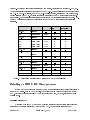
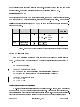
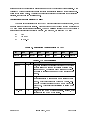
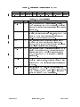
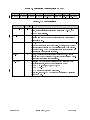
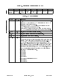
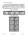
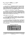
IBM 5x86C Microprocessor ® BIOS Writer's Guide Application Note Introduction Revision Summary: This revision updates the processor name, corrects the device ID, corrects the description of linear burst, deletes the CPUID instruction, corrects several register names and field names and makes several minor editorial corrections. Caution: Refer to the errata that pertain to the revision level of your hardware before activating any of the features described in this Application Note. This document is intended for IBM 5x86C microprocessor system BIOS writers. It is not a stand alone document but supplements other IBM 5x86C microprocessor documentation, including the IBM 5x86C microprocessor data book and IBM 5x86C microprocessor adaptation guides. This document includes information on IBM 5x86C microprocessor detection, 5x86C mi- croprocessor configuration register definition, and recommendations for configuration register programming. This document only discusses the differences between the IBM 486DX2 and the IBM 5x86C microprocessor that may affect BIOS programming. Configuration Register Index Assignments The IBM 5x86C processor provides on-chip configuration registers used to control the on-chip cache, system management mode (SMM) and other IBM 5x86C microprocessor unique features. Access to the configuration registers is achieved by writing the index of the register to I/O port 22h. I/O port 23h is then used for data transfer. Each I/O port 23h data transfer must be preceded by an I/O port 22h register index selection, otherwise the second and later I/O port 23h operations are directed off-chip and produce external I/O cycles. always directed off-chip. Reads of I/O port 22h are Table 1 lists the IBM 5x86C microprocessor configuration register in- dex assignments. After reset, configuration registers with indexes within C0-CFh and FE-FFh are accessible. In order to prevent potential conflicts with other devices which may use ports 22 and 23h to access their registers, the remaining registers (indexes 20, D0-FDh) are accessible only if the MAPEN(3-0) bits in CCR3 are set to 0001b. Page 1 of 16 With MAPEN(3-0) = 0001b, any access to indexes September 27, 1995 Fax #40038 in the 00-FFh range will not create external I/O bus cycles. Registers with indexes C0-CFh, FE- FFh are accessible regardless of the state of MAPEN(3-0). If the register index number is outside the C0-CFh or FE-FFh ranges, and MAPEN(3-0) are set to zeros, external I/O bus cycles occur. Table 1 lists the MAPEN(3-0) values required to access each 5x86C microprocessor configuration register. The configuration registers are described in more detail later in this document. Ap- pendix A contains example code for accessing the IBM 5x86C microprocessor configuration registers. Register Index Register Name 00h-1Fh Reserved 20h Performance 21h-C0h Reserved C1h Config Cntl 1 C2h Config Cntl 2 C3h E8h C5h-CCh Reserved CDh-CFh Acronym Width in MAPEN(3-0) Bits for Access -- -- -- PCR0 8 1 -- -- CCR1 8 x CCR2 8 x Config Cntl 3 CCR3 8 x Config Cntl 4 CCR4 8 x -- -- -- SMAR 24 x -- -- -- CCR4 8 1 -- -- -- PMR 8 1 -- -- -- SMM Address Region D0h-E7h Reserved E8h Config Cntl 4 E9h-EFh Reserved F0h Power Mgmt F1h-FDh Reserved FEh Device ID 0 DIR0 8 x FFh Device ID 1 DIR1 8 x Table 1. Configuration Register Index Assignments (Note: x = don't care) Detecting an IBM 5x86C Microprocessor System BIOS can determine if an IBM 5x86C microprocessor exists by first determining if an IBM CPU exists. CPU. If an IBM CPU exists, the CPU's DIRs can be read to identify the type of Previous versions of IBM's CPUs did not contain the DIRs, however, all current CPU's contain DIRs. Detecting an IBM CPU Detection of an IBM CPU is done by checking the state of the undefined flags following execution of the divide instruction which divides 5 by 2. Page 2 of 16 September 27, 1995 The undefined flags in an IBM Fax #40038 microprocessor remain unchanged following the divide. undefined flags. An Intel® device will modify some of the Appendix B contains example code for detecting an IBM CPU. Identifying an IBM CPU Once it is determined that an IBM microprocessor exists, its DIRs can be read to identify its type. The DIRs contain CPU device identification, stepping and revision information. subset of the IBM 5x86C microprocessor's configuration registers. The DIRs are a The IBM 5x86C microproc- essor's DIRs exist at register indexes FEh and FFh as shown in Table 1 and contain the information shown in Table 2. Register Description Bit Position Contents Core/Bus Clock Ratio DIR0 Device ID Reg 0 7-0 DEVID(7-0)= 29h or 2/1 2Bh DEVID(7-0)= 2Dh or 3/1 2Fh DIR1 Device Stepping 7-4 SID(3-0)=xxh Device Revision 3-0 RID(3-0)=xxh Table 2. IBM 5x86C Microprocessor Device Identification Register Contents CPU EDX Value After RESET Some CPU detection algorithms may use the value of the CPU's EDX register following RESET. The IBM 5x86C microprocessor's EDX register contents following reset are shown below. EDX[31:16] = undefined Stepping 0, Revision 1 and earlier EDX[15:8] = DIR1 (same contents as Device Identification Register 1) EDX[7:0] = DIR0 (same contents as Device Identification Register 0) Stepping 0, Revision 2 and later EDX[15:8] = 04h EDX[7:0] = 90h Configuration Register Bit Definitions On-chip configuration registers are used to control the on-chip cache, system management mode and other IBM 5x86C microprocessor unique features. All bits in the configuration regis- ters are initialized to zero following reset unless specified otherwise. tings will vary depending on system design. Page 3 of 16 The appropriate register set- Therefore, the BIOS creating utilities or setup September 27, 1995 Fax #40038 screens must have the capability to easily define and modify the contents of these registers. This will allow OEMs and integrators to easily configure these register settings with the values appropriate for the system design. The following paragraphs describe the categories of configuration registers, their purpose and bit assignments. Configuration Control Registers CCR(1-4) There are seven registers in the IBM 5x86C microprocessor that control the cache, power management and other unique features. Figures 1 through 6 and Tables 3 through 8 describe the CCRs and briefly describe their applications. The BIOS utilities must allow for OEMs to create a setup screen that includes the ability to program, at a minimum, the following CCR bits: a) WT1 b) LINBRST c) IORT(2-0) Figure 1. Configuration Control Register 1 (CCR1) Bit 7 Bit 6 Bit 5 Bit 4 Bit 3 Reserved Reserved Reserved Reserved MMAC Bit 2 SMAC Bit 1 Bit 0 USE_SMI Reserved Table 3. CCR1 Bit Definitions Bit Name MMAC Bit No. 3 Description If set, data accesses to addresses within the SMM address space are issued to main memory instead of system management memory. This is only used within an SMM serv- ice routine to access normal memory which overlaps SMM memory. SMAC 2 If set, any access to addresses within the SMM address space access system management memory instead of main memory. SMI# input is ignored while SMAC is set. Set- ting SMAC=1 allows access to SMM memory without entering SMM. This is useful for initializing or testing SMM memory. USE_SMI 1 If set, SMI# and SMADS# pins are enabled. If clear, SMI# pin is ignored and SMADS# pin floats. Page 4 of 16 September 27, 1995 Fax #40038 Figure 2. Configuration Control Register 2 (CCR2) Bit 7 Bit 6 USE_SUSP BWRT Bit 5 Bit 4 Bit 3 Bit 2 Bit 1 Bit 0 Reserved WT1 SUSP_HLT LOCK_NW USE_WBAK Reserved Table 4. CCR2 Bit Definitions Bit NAME USE_SUSP Bit No. 7 Description If set, SUSP# and SUSPA# pins are enabled. SUSP# pin is ignored and SUSPA# pin floats. If clear, These pins should only be enabled if the external system logic (chipset) supports them. BWRT 6 If set, enables burst write cycles. This should only be set if the system logic supports burst writes. If set, the CPU will perform a 4 dword burst write on line replacements and write-back cycles as a result of snoop hits. WT1 4 If set, designates that any cacheable accesses in the 640 KBytes to 1 MByte address region are defined writethrough. With WT1=1, any write to a cached value in this range will also get issued to the external bus. SUSP_HLT 3 If set, execution of the HLT instruction causes the CPU to enter low power suspend mode. This bit should be used cautiously since the CPU must recognize and service an INTR, NMI, SMI or RESET to exit the "HLT initiated" suspend mode. LOCK_NW 2 If set, the NW bit in CR0 becomes read only, and the CPU ignores any writes to this bit. This should be set to 1 after setting the CR0 NW to prevent inadvertent modification of the NW bit. USE_WBAK 1 If set, enables the CPU write-back cache interface pins which include CACHE#, INVAL, WM_RST, and HITM#. If WBAK is set to 0, INVAL and WM_RST are ignored and the HITM# and CACHE# outputs float. Page 5 of 16 September 27, 1995 Fax #40038 Figure 3. Configuration Control Register 3 (CCR3) Bit 7 Bit 6 Bit 5 Bit 4 MAPEN3 MAPEN2 MAPEN1 MAPEN0 Bit 3 Bit 2 Bit 1 Bit 0 SMM_MODE LINBRST NMI_EN SMI_LOCK Table 5. CCR3 Bit Definitions Bit Name MAPEN(3-0) Bit No. 7-4 Description If set to 0001b, all configuration registers are accessible. If clear, only configuration registers with indexes C0-CFh, FEh and FFh are accessible. SMM_MODE 3 If set, the CPU's SMM hardware interface pins are redefined to function like the SMM hardware interface pins on the Intel SL Enhanced 486. LINBRST 2 If set, the IBM 5x86C microprocessor will use linear address sequence when performing burst cycles. If clear, the IBM 5x86C microprocessor will use a 1+4 address sequence when performing burst cycles. The 1+4 address sequence is compatible with the Intel 486 burst address sequence. NMI_EN 1 If set, NMI interrupt is recognized while in SMM. This bit should only be set while in SMM, after the appropriate NMI interrupt service routine has been setup. SMI_LOCK 0 If set, the CPU prevents modification of the following SMM configuration bits, except when operating in SMM: CCR1 USE_SMI,SMAC,MMAC,SM3 CCR3 NMI_EN SMAR Starting address and block size. Once set, the SMI_LOCK bit can only be cleared by asserting the RESET pin. Page 6 of 16 September 27, 1995 Fax #40038 Figure 4. Configuration Control Register 4 (CCR4) Bit 7 Bit 6 Bit 5 Bit CPUIDEN Reserved Reserved Reserved FP_FAST 4 Bit DTE_EN 3 Bit 2 MEM_BYP IORT(2) Bit 1 Bit IORT(1) 0 IORT(0) Table 6. CCR4 Bit Definitions Bit Name CPUIDEN BitNo. 7 Description If set, bit 21 of the EFLAG register may be read or written (indicating the CPU supports the CPUID instruction) and the CPUID instruction will execute normally. If clear, bit 21 of the EFLAG register is not writeable and the CPUID instruction is an invalid opcode. (This bit is only available on stepping level 1 and later devices. The CPUID instruction is an invlaid opcode on all prior devices. FP_FAST 5.00 DTE_EN 4 If set, the Directory Table Entry cache is enabled. MEM_BYP 3 If set, enables memory read bypassing. IORT(2-0) 2-0 If set, fast FPU exception reporting enabled. Specifies the minimum number of bus clocks between I/O accesses (I/O recovery time). The delay time is the minimum time from the beginning of one I/O cycle to the beginning of the next (i.e. ADS# to ADS# time). The default I/O recovery time is set to 32 bus clocks (0.97 microsecs at 33MHz, 0.60 microsecs at 50MHz). If the BIOS already has I/O recovery time implemented via other mechanisms (delay instructions, dummy I/O cycles, etc.), the IBM 5x86C microprocessor programmed delay may be eliminated to minimize I/O cycle separation time. 0h=no delay 1h=2 clocks 2h=4 clocks 3h=8 clocks 4h=16 clocks 5h=32 clocks (default after RESET) 6h=64 clocks 7h=128 clocks Page 7 of 16 September 27, 1995 Fax #40038 Figure 5. Power Management Register - PMR Bit 7 Bit 6 Bit 5 Bit 4 Bit 3 Bit 2 Reserved Reserved Reserved Reserved Reserved HLF_CLK Bit 1 CLK(1) Bit 0 CLK(0) CLK(2) Table 7. PMR Bit Definitions Bit Name HLF_CLK Bit No. 2 CLK(2) Description If set, the core clock frequency will run at half the external bus frequency. When an external bus transfer occurs, the core clock fre- quency will automatically increase in frequency for the duration of the transfer. When the transfer is complete, the core will revert to half the frequency of the bus. CLK(1:0) 1-0 The CLK(1:0) bits can be used to change the internal core frequency relative to the bus frequency at any time. Any attempt to modify the core frequency higher than specified for the device will be ignored. These bits are initialized during reset to the clock specified by the device (i.e. 2X, 3X, etc.). The following core/bus frequency ratios are available: Page 8 of 16 HLF_CLK = 1 CLK(1:0)=xx: 1/2 (core/bus) HLF_CLK = 0 CLK(1:0)=00: 1/1 HLF_CLK = 0 CLK(1:0)=01: 2/1 HLF_CLK = 0 CLK(1:0)=10: 3/1 HLF_CLK = 0 CLK(1:0)=11: Reserved September 27, 1995 Fax #40038 SMM Address Region Register - SMAR The SMAR is used to define the SMM memory region. The SMAR has three 8-bit regis- ters associated with it which define the region starting address and block size. Table 8 below shows the format for the SMAR and lists the index assignments for the SMAR starting address and block size. The region starting address is defined by the upper 12 bits of the physical address. The region size is defined by BSIZE(3:0) [bits 3:0 of SMAR). The BIOS and its utilities should allow for definition of the SMAR. There is one restriction when defining the SMM address region. The region starting address must be on a block size boundary. For example, a 128KByte block is allowed to have a starting address of 0K, 128K, 256K, and so on. Table 8. SMAR Index assignments Starting Address Region Block Size A31 - A24 A23 - A16 A15 - A12 BSIZE (3-0) Bits (7-0) Bits (7-0) Bits (7-4) Bits (3-0) CDh CEh CFh Table 9. BSIZE(3-0) Bit Definitions Page 9 of 16 BSIZE (3-0) Region Size 0h Disabled 1h 4 KBytes 2h 8 KBytes 3h 16 KBytes 4h 32 KBytes 5h 64 KBytes 6h 128 KBytes 7h 256 KBytes 8h 512 KBytes 9h 1 MBytes Ah 2 MBytes Bh 4 MBytes Ch 8 MBytes Dh 16 MBytes Eh 32 MBytes Fh 4 GBytes September 27, 1995 Fax #40038 Performance Control Configuration Register - PCR0 PERF The performance Control Configuration register is used to turn on several of the performance features of the IBM 5x86C microprocessor. set to 1. For maximum performance bits 0-2 should be Please refer to the errata for each revision level of hardware for information on these bits. Figure 6. Performance Configuration Register Bit 7 Bit 6 Bit 5 Bit 4 Bit 3 Bit 2 Bit 1 Bit 0 LSSER Reserved Reserved Reserved Reserved LOOP_EN BTB_EN RSTK_EN Reserved Rstack Table 10. PERF(2-0) Bit Definitions Bit Name Description Bit No. LSSER 7 If set, all memory reads and writes will occur in execution order. LOOP 2 If set, enables faster support for loops. 1 If set, 0 If set, enables the call return stack. _EN BTB_EN RSTK_EN enables the Branch Target Buffer for branch prediction. RStack Table 11. Required field settings for Rev. 1.4.2 Register Field/Value Effect CCR2 BWRT = 0 Burst write cycles disabled CCR4 MEM_BYP = 1 On for performance DTE_EN = 1 Enables Directory Table Entry Cache FP_FAST = 0 Fast FPU error reporting off IORT(2-0) = 0 Errata fix SMCDIS= 0 Enable self-modified code checking HLF_CLK = 0 Core clock runs at bus speed when bus interface is idle. CLK Maintain default setting 11=3x or 01=2x RSTACK = 0 Off - Errata fix BTB = 0 Off - For WinStone, problem rarely occurs LOOP = 0 Off - Errata fix LSSR = 1 Store read/write ordering for PCI memory mapped devices LSSR = 0 For Systems without PCI PMR PCR0 Page 10 of 16 September 27, 1995 Fax #40038 Programming Model Differences vs i486 INVD and WBINVD Instructions The INVD and WBINVD instructions are used to invalidate the contents of the internal and external caches. The WBINVD instruction first writes back any modified lines in the cache and then invalidates the contents. It ensures that cache coherency with system memory will be maintained regardless of the cache operating mode, write-through or write-back. Following in- validation of the internal cache, the CPU generates special bus cycles to indicate that external caches sould also write back modified data and invalidate their contents. On the IBM 5x86C microprocessor, the INVD instruction functions identically to the WBINVD instruction. The IBM 5x86C microprocessor always writes all modified internal cache data to external memory prior to invalidating the internal cache contents. In contrast, the Pentium invalidate the contents of its internal cache without writing back the "dirty" data to system mem- 1 ory . The technique employed in the IBM 5x86C microprocessor precludes the possibility of data incoherency between the CPU's internal cache and system memory. Control Register 0 (CR0) CD and NW Bits The CPU's CR0 register contains, among other things, the CD and NW bits which are used to control the on-chip cache. CR0, like the other system level registers, is only accessible to programs running at privilege 0, the highest privilege level. Table 12 lists the cache operating modes for the possible states of the CD and NW bits. The CD and NW bits are set to one (cache disabled) after reset. For highest performance the cache should be enabled in write-back mode by setting the CD=0 and NW=1. for enabling the cache is in Appendix C. CD and NW be set to 1. setting CD=1. Sample code To completely disable the cache, it is recommended that On the IBM 5x86C microprocessor the cache can be disabled by only The IBM 5x86C microprocessor cache will always accept invalidation cycles even when the cache is disabled. Table 12. Cache Operating Modes 1 CD NW Operating Modes 1 1 Cache disabled 1 0 Cache disabled 0 1 Cache enabled in Write-back mode 0 0 Cache enabled in Write-through mode See Pentium Family User's Manual, Volume 3: Architecture and Programming Manual Page 11 of 16 September 27, 1995 Fax #40038 Initialization Sequence The IBM 5x86C microprocessor features and capabilities described above should be enabled/initialized during BIOS POST. Below is a recommended sequence for initializing the IBM 5x86C microprocessor. 1) Program I/O recovery time using IORT(2-0) in CCR4. 2) Program WT1. 3) Define SMAR. 4) Program USE_SUSP 5) Program SUSP_HLT 6) Enable cache (see Appendix C for example code). 7) Program LOCK_NW. 8) Initialize/enable SMM (see BL486DX2 SMM Programmer's Guide) Page 12 of 16 September 27, 1995 Fax #40038 Appendix A - Programming IBM 5x86C Microprocessor Configuration Registers Sample code for setting USE_SMI=1 in CCR1 mov out in or mov mov out mov out al, 0c1h 22h, al al, 23h al, 02h ah, al al, 0c1h 22h, al al,ah 23h, al Page 13 of 16 ; set index for CCR1 ; select CCR1 register ; read current CCR1 value ; set USE_SMI bit ; save set bit data in ah ; set index for CCR1 ; select CCR1 register ; get back saved data to al ; write new value to CCR1 September 27, 1995 Fax #40038 Appendix B - Detecting An IBM 5x86C Microprocessor assume cs:_TEXT public _ism1sc _TEXT segment byte public 'CODE' ;********************************** ; Function: int isibm () ; Purpose: Determine if IBM 5x86C CPU is present ; Technique: IBM 5x86C CPUs do not change flags where flags ; change in an undefined manner on other CPUs ; Inputs: none ; Output: ax == 1 if IBM 5x86C present, 0 if not ;*********************************** _ism1sc proc near .486 xor ax, ax ; clear ax sahf ; clear flags, bit 1 always=1 in flags mov ax, 5 mov bx, 2 div bl ; operation that doesn't change flags on IBM 5x86C parts lahf ; get flags cmp ah, 2 ; check for change in flags jne not_m1sc ; if flags changed, it is not IBM 5x86C mov ax, 1 ; true IBM 5x86C CPU jmp done not_m1sc: mov ax, 0 ; non-IBM 5x86C CPU done: ret _ism1sc endp _TEXT ends end Page 14 of 16 September 27, 1995 Fax #40038 Appendix C - Enabling The IBM 5x86C Microprocessor Cache Sample code for enabling the IBM 5x86C microprocessor write-back cache and setting LOCK-NW=1. ;**** disable cache mov eax, cr0 or eax, 040000000h mov cr0, eax ; CD bit in CR0 = 1 ;**** write back and invalidate the cache wbinvd ;**** enable write back mode mov eax, cr0 and eax, 0ffffffffh mov cr0, eax ; NW bit in CR0 = 1 ;**** set LOCK_NW=1 to prevent modification of NW ;**** mov al, 0c2h ; set index for CCR2 out 22h, al ; select CCR2 register in al, 23h ; read current CCR2 value or al, 04h ; set LOCK_NW=1 mov ah,al ; save or'd data in ah mov al, 0c2h ; set index for CCR2 out 22h, al ; select CCR2 register mov al,ah ; get back saved data into al out 23h, al ; write new value to CCR2 enable cache mov eax, cr0 and eax, 0bfffffffh mov cr0, eax Page 15 of 16 ; CD bit in CR0 = 0 September 27, 1995 Fax #40038 IBM Corporation 1995. All rights reserved. IBM and the IBM logo are registered trademarks of International Business Machines Corporation. IBM Microelectronics is a trademark of the IBM Corp. All other product and company names are trademarks/registered trademarks of their respective holders. 1995 IBM Corp. This document may contain preliminary information and is subject to change by IBM without notice. IBM makes no representations or warranties that the use of the information or applications herein shall be free of third party intellectual property claims and assumes no responsibility or liability from any use of the information contained herein. Nothing in this document shall operate as an express or implied license or indemnity under the intellectual property rights of IBM or third parties. The products described in this document are not intended for use in implantation or other direct life support applications where malfunction may result in physical harm or injury to persons. NO WARRANTIES OF ANY KIND, INCLUDING BUT NOT LIMITED TO THE IMPLIED WARRANTIES OF MERCHANTABILITY OR FITNESS FOR A PARTICULAR PURPOSE ARE OFFERED IN THIS DOCUMENT. All performance data contained in this publication was obtained in a specific environment, and is presented as an illustration. The results obtained in other operating environments may vary. Page 16 of 16 September 27, 1995 Fax #40038