1
APPLICATION NOTE
M16C/63, 64, 64A, 64C, 65, 65C, 6C, 5LD,
56D, 5L, 56, 5M, and 57 Groups
Use of User Boot Function
1.
R01AN0403EJ0102
Rev. 1.02
Dec. 28, 2011
Abstract
This document describes the method for rewriting the MCU internal flash memory (data flash, program
ROM 1) using the user boot function in M16C/63, 64, 64A, 64C, 65 (products with 512 KB or less of
program ROM 1 only), 65C, 6C, 5LD, 56D, 5L, 56, 5M, and 57 Group products.
The user boot function is for rewriting the MCU internal flash memory with a user-selected communication
method.
(The user boot function is not the start up function of the user application program.)
This application note describes the user boot function using the M16C/64 Group.
2.
Introduction
The application example described in this document applies to the following MCUs:
MCUs: M16/63, 64, 64A, 64C, 65 (products with 512 KB or less of program ROM 1 only)(1),
65C, 6C, 5LD, 56D, 5L, 56, 5M, 57 Groups
Oscillation frequency: 8 MHz
Operation frequency: 24 MHz (8 MHz in CPU rewrite mode)
Note:
1. MCUs with more than 512 KB of program ROM 1 have different software commands. Refer to
the hardware manual for details.
Careful evaluation is recommended before using the program described in this application note.
R01AN0403EJ0102 Rev. 1.02
Dec. 28, 2011
Page 1 of 28
M16C/63, 64, 64A, 64C, 65, 65C, 6C, 5LD, 56D, 5L, 56, 5M, and 57 Groups
3.
Use of User Boot Function
Application
3.1
Outline
In this application note, control rewriting the MCU flash memory using serial communication from the host
PC. Xmodem is used to transmit the MOTOROLA-S format. This application note introduces the following
three methods regarding rewrite operation: normal programming, erase ignoring the lock bit status, and
erase not ignoring the lock bit status.
3.2
Introduction of User Boot Function
M16C/63, 64, 64A, 64C, 65 (products with 512 KB or less of program ROM 1 only), 65C, 6C, 5LD, 56D,
5L, 56, 5M, and 57 Group products have the user boot function in boot mode. When the MCU starts in
boot mode (operated after hardware reset occurs while a low-level signal is applied to the P5_5 pin and a
high-level signal is applied to pins CNVSS and P5_0), user boot mode or standard serial I/O mode can be
selected in accordance with the content of the user boot code area.
In user boot mode, the program written into the program ROM 2 area (starts from 10000h) on flash
memory is executed.
The features of flash memory rewrite operation in user boot mode are described below.
• Ports (pins) for entry are freely selectable
UART1 is used in standard serial I/O mode.
• Serial programmer(1) is freely selectable
Protocols including communication method, contents of transmit/receive data (command, program
code), and communication timing can be designed.
Note:
1. In standard serial I/O mode, a serial programmer supporting M16C/63, 64, 64A, 64C, 65, 65C, 6C,
5LD, 56D, 5L, 56, 5M, and 57 Groups is necessary.
R01AN0403EJ0102 Rev. 1.02
Dec. 28, 2011
Page 2 of 28
M16C/63, 64, 64A, 64C, 65, 65C, 6C, 5LD, 56D, 5L, 56, 5M, and 57 Groups
3.3
Use of User Boot Function
Memory Map of Program ROM 2
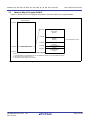
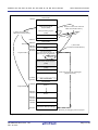
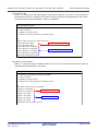
Figure 3.1 shows the user boot program area and the user boot code area in program ROM 2.
Program ROM 2
010000h
User boot program area
013FF0h
Boot code
(8-byte)
013FF8h
013FFAh
013FF0h
User boot code area
013FFBh
013FFCh
013FFFh
Address (1)
(2-byte)
Port information for entry
Bit (2)
(1-byte)
Start level select (3)
(1-byte)
Reserved space
(4-byte)
Notes:
1. Port address for entry (Example: For P0, the address is 03E0h; for P1, the address is 03F4h)
2. Bit number of port for entry (0 to 7)
3. Port level for entry (high: 01h, low: 00h)
Figure 3.1
The User Boot Program Area and The User Boot Code Area
R01AN0403EJ0102 Rev. 1.02
Dec. 28, 2011
Page 3 of 28
Use of User Boot Function
M16C/63, 64, 64A, 64C, 65, 65C, 6C, 5LD, 56D, 5L, 56, 5M, and 57 Groups
3.4
Set Values in the User Boot Code Area and Start Mode
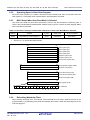
Set values in the user boot code area and the corresponding start mode are described below where port
Pi_j (i = 0 to 10, j = 0 to 7) is selected for entry. Table 3.1 lists Set Values in the User Boot Code Area and
Start Mode. Only use the values listed in Table 3.1.
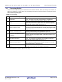
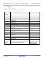
Table 3.1 Set Values in the User Boot Code Area and Start Mode
Port Information for Entry
Boot Code
(13FF0h to 13FF7h)
Address
(13FF8h to
13FF9h)
Bit
(13FFAh)
Start level
select
(13FFBh)
00000000h
00h
"UserBoot"(1)
Pi register
address(2)
00h to 07h
(value of j)
—
Start Mode
—
User boot mode
High
Standard serial I/O
mode
Low
User boot mode
High
User boot mode
Low
Standard serial I/O
mode
—
—
Standard serial I/O
mode
13FF4h
13FF5h
01h
Other than "UserBoot"
Port
Pi_j
Input
Level
—
Notes:
1. See Table 3.2 "UserBoot" in ASCII Code.
2. See Table 3.3 Addresses of Selectable Ports for Entry.
Table 3.2 "UserBoot" in ASCII Code
Address
13FF0h
13FF1h
13FF2h
13FF3h
13FF6h
13FF7h
ASCII
55h
73h
65h
72h
42h
6Fh
6Fh
74h
Code (upper-case U) (lower-case s) (lower-case e) (lower-case r) (upper-case B) (lower-case o) (lower-case o) (lower-case t)
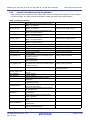
Table 3.3 Addresses of Selectable Ports for Entry
Port
Pi Register Address
P0
03E0h
P1
03E1h
P2
03E4h
P3
03E5h
P4
03E8h
P5(1)
03E9h
P6
03ECh
P7
03EDh
P8
03F0h
P9
03F1h
P10
03F4h
Note:
1. The user boot mode is always selected as start mode if "UserBoot" is set to boot code while in either
of the following conditions:
• P5_0 is selected as a port information for entry and high level is selected as start level.
• P5_5 is selected as a port information for entry and low level is selected as start level.
R01AN0403EJ0102 Rev. 1.02
Dec. 28, 2011
Page 4 of 28
M16C/63, 64, 64A, 64C, 65, 65C, 6C, 5LD, 56D, 5L, 56, 5M, and 57 Groups
3.4.1
Use of User Boot Function
Configuration Example for User Boot Code Area
The user boot code area is set as ROMDATA of user boot program.
Configuration example for user boot code area on the following conditions:
Section name is "ubtcd_sec".
Port P10 (P10) is selected as a port for entry.
Bit 0 (P10_0) is selected as a bit for entry.
High is selected as start level.
<Section definition>
- When section address is specified in assembly language
;---------------------------------------------------------------;
User boot code area section
;---------------------------------------------------------------.section
ubtcd_sec, ROMDATA
.org
013FF0H
.section
ubtcd_sec_FE, ROMDATA, ALIGN
- When section address is specified in the linkage editor (ln30)
Add "-ORDER ubtcd_sec_FE=13FF0" to the command option in ln30.
<User boot code area definition >
/*----------------------------------------------------------------------------------------*/
/*
define of "User boot code area"
/*----------------------------------------------------------------------------------------*/
typedef struct UBTCD_DEF {
unsigned char btcd[8];
/* Boot-code */
unsigned short eptaddr;
/* SFR address of entry port */
unsigned char eptbitn;
/* Bit of the entry port */
unsigned char exptlvl;
/* Enable port level */
unsigned long ubtrsv;
/* Reserved area */
} ubtcd_def;
#pragma SECTION rom ubtcd_sec
/* The section name "rom" is changed to "ubtcd_sec". */
const far ubtcd_def UserBootCode = {{'U','s','e','r','B','o','o','t'},
/* Boot-code
= "UserBoot" */
0x03F4,
/* Entry port
= "P10" */
0x00,
/* Entry port bit = bit0 */
0x01,
/* Enable port level = "H" */
0xFFFFFFFF
/* Reserved area */
};
#pragma SECTION rom rom
/* The section name is returned to "rom". */
R01AN0403EJ0102 Rev. 1.02
Dec. 28, 2011
Page 5 of 28
M16C/63, 64, 64A, 64C, 65, 65C, 6C, 5LD, 56D, 5L, 56, 5M, and 57 Groups
3.5
Use of User Boot Function
Notes on User Boot Program
User boot program code should fit in the program ROM 2 area. Also, start address of execution is 10000h
in user boot mode.
When a user boot program is debugged using an on-chip debugger, set the reset vector value to 10000h
and then turn on in single-chip mode.
Also, do not erase the block including the reset vector.
3.5.1
Rewriting Flash Memory
To rewrite the flash memory (data flash, program ROM 1), both EW0 mode and the EW1 mode of CPU
rewrite mode can be used.
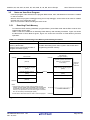
Table 3.4 lists the Limitations on Rewriting Flash Memory and Handling Procedure. Figure 3.2 shows
the Relocation of User Boot Program, Figure 3.3 shows the Overview of Flash Memory Rewrite
Operation.
Table 3.4 Limitations on Rewriting Flash Memory and Handling Procedure
Limitations
Flash memory can be erased on a
block-by-block basis.
(Flash memory has a finite number of
program and erase cycles.)
Handling Procedure
Consider decreasing block erase cycles in block units when
programming the flash memory.
Internal ROM
(Program ROM 2)
Internal RAM
010000h
000400h
(Note 2)
Flash memory rewrite program
(RAM)
Interrupt handling program
(RAM)
User boot program
(Rewrite operation to the flash
memory is not performed
in this area.)
User boot
program
code area
Flash memory rewrite program
(ROM)
(Note 1)
Interrupt handling program
(ROM)
Relocatable vector table (RAM)
Relocatable vector table (ROM)
(Note 2)
00XXFFh
Notes:
1. Transfer flash memory rewrite program (ROM), interrupt
handling program (ROM), and relocatable vector table (ROM)
to the RAM in the area where rewrite operation to the flash
memory is not performed in the user boot program code area.
Also, set the Interrupt Table Register (INTB).
2. Work RAM or stack area which is used in user boot program.
Figure 3.2
013FF0h
User boot code area
013FFFh
Relocation of User Boot Program
R01AN0403EJ0102 Rev. 1.02
Dec. 28, 2011
Page 6 of 28
M16C/63, 64, 64A, 64C, 65, 65C, 6C, 5LD, 56D, 5L, 56, 5M, and 57 Groups
Use of User Boot Function
Internal RAM
000400h
Flash memory rewrite
program (RAM)
4) Write, erase, read and
blank check to flash memory
3) Request to write, erase, read and
blank check to flash memory
Interrupt handling program
(RAM)
Relocatable vector tables (RAM)
te
ction in
ral fun st
e
h
ip
r
Pe
reque
rrupts
00XXFFh
Internal ROM
Data flash
00E000h
00EFFFh
00F000h
00FFFFh
010000h
Program ROM 2
Block A
Block B
1) Boot mode
(User boot mode selection)
User boot program
(The area where rewrite to the
flash memory is not performed.)
Waiting for
2)
command
Flash memory rewrite program
(ROM)
Interrupt handling program
(ROM)
Relocatable vector table (ROM)
When user boot program is debugged
(Single-chip mode)
013FF0h
013FFFh
User boot code area
Internal ROM
0X0000h
Block N
Program ROM 1
0XFFFFh
0D0000h
Block 2
0DFFFFh
0E0000h
Block 1
0EFFFFh
0F0000h
Block 0
Fixed vector tables (for debug) (1)
0FFFFFh
Figure 3.3
Note:
1. Necessary for debugging user boot program.
Overview of Flash Memory Rewrite Operation
R01AN0403EJ0102 Rev. 1.02
Dec. 28, 2011
Page 7 of 28
Use of User Boot Function
M16C/63, 64, 64A, 64C, 65, 65C, 6C, 5LD, 56D, 5L, 56, 5M, and 57 Groups
3.5.2
Operating Speed of User Boot Program
Set a CPU clock frequency of 10 MHz or less when in CPU rewrite mode. Also, set the PM17 bit in the
PM1 register to 1 (wait state) when internal RAM or internal ROM is accessed.
3.5.3
MCU Status When User Boot Mode is Selected
The value in the SFR is a value after reset and the value in the internal RAM is undefined. (Also, a
value in the internal RAM is undefined after software reset.) Figure 3.4 shows the CPU Register Status
When User Boot is Selected.
Table 3.5 SFR which Changes Is Status after CPU Reset or when User Boot Mode is Selected
Address
Register
Symbol
Reset Value
Value when User Boot
Mode is Selected
0220h
Flash Memory Control Register 0
FMR0
0000 0001b
0010 0001b(1)
Note:
1. Set bit 5 to 1 to operate the FMR0 resister.
b15
b0
0000h
Data register (R0)
0000h
Data register (R1)
0000h
Data register (R2)
0000h
Data register (R3)
0000h
Address register (A0)
0000h
Address register (A1)
0000h
Frame base register (FB)
b0
b19
00000h
Interrupt table register (INTB)
Address 10000h
Program counter (PC)
b15
b0
0000h
0000h
User stack pointer (USP)
Interrupt stack pointer (ISP)
0000h
Static base register (SB)
b15
b0
Flag register (FLG)
b15
X
Figure 3.4
3.5.4
0
0
IPL
0
X
X
X
b8
b7
X
0
0
X
0
X
X
X
X
U
I
O
B
S
Z
D
C
b0
X: Undefined
CPU Register Status When User Boot is Selected
Refreshing Watchdog Timer
When starting watchdog timer, for example, when WDTON bit in the OSF1 (address FFFFh) in the
program ROM 1 is 0 (watchdog timer starts automatically after reset), refresh the watchdog timer in the
user boot program.
R01AN0403EJ0102 Rev. 1.02
Dec. 28, 2011
Page 8 of 28
M16C/63, 64, 64A, 64C, 65, 65C, 6C, 5LD, 56D, 5L, 56, 5M, and 57 Groups
3.6
Use of User Boot Function
Processing of User Boot Mode Selection
Figure 3.5 shows the Processing of User Boot Mode Selection.
Pins are configured for boot mode entry.
- CNVSS is high
- P5_0 is high
- P5_5 is low
- Reset
- Software reset
- Watchdog timer reset
- Voltage monitor reset
- Oscillation stop detect reset
Boot mode determination
User boot mode is enabled
by user boot code area setting
User boot mode
Figure 3.5
User boot mode is disabled
by user boot code area setting
Standard serial I/O mode
Processing of User Boot Mode Selection
R01AN0403EJ0102 Rev. 1.02
Dec. 28, 2011
Page 9 of 28
M16C/63, 64, 64A, 64C, 65, 65C, 6C, 5LD, 56D, 5L, 56, 5M, and 57 Groups
4.
Use of User Boot Function
Sample User Boot Programs
4.1
Overview
Program the internal flash memory using CPU rewrite mode (EW0 mode) and the user boot function in
M16C/63, 64, 64A, 64C, 65 (products with 512 KB or less of program ROM 1 only), 65C, 6C, 5LD, 56D,
5L, 56, 5M, and 57 Group products.
Programming targets
• Data flash (blocks A and B)
• Program ROM 1
Processing for the flash memory is transferred using a terminal software(1) running on a host PC.
Data written to the internal flash memory is MOTOROLA-S formatted text data and is transferred using
XMODEM protocol(2).
The received MOTOROLA-S formatted data is converted to binary data and then written to the internal
flash memory.
Notes:
1. The communication settings in the terminal software are as follows:
Bits per second: 115200
Data length: 8 bits
Parity: None
Stop bit: 1
Flow control: None
2. Only the S1 record (16-bit address length) and S2 record (24-bit address length) are processed
as data to program.
4.2
Connecting to the Host PC
A target MCU board and a host PC are connected with an RS-232C cable.
Target board(3)
PC (D-sub 9-pin male)
Pin No.
1
2
3
4
5
6
7
8
9
Signal
CD
RXD
TXD
DTR
GND
DSR
RTS
CTS
RI
R01AN0403EJ0102 Rev. 1.02
Dec. 28, 2011
Pin Name
NC(2)
(Note 1)
(Note 1)
P6_3/TXD0
P6_2/RXD0
VSS
NC(2)
NC(2)
NC(2)
NC(2)
NC(2)
Notes:
1. Signal level conversion circuit is necessary.
2. These pins are not used in the sample user boot program.
3. Pins for boot mode entry are not described in this figure.
Page 10 of 28
M16C/63, 64, 64A, 64C, 65, 65C, 6C, 5LD, 56D, 5L, 56, 5M, and 57 Groups
4.2.1
Use of User Boot Function
Pins Used
Table 4.1 Pins Used and Their Functions
Item
I/O
Power Supply
VCC1
Input
—
Supply voltage
VCC2
Input
—
Supply voltage
VSS
Input
—
0 V input
Reset input
RESET
Input
VCC1
—
CNVSS
CNVSS
Input
VCC1
VCC1 input(1)
P5_0(CE) / WRL / WR
Input
VCC2
VCC2 input(1)
P5_5(EPM) / HOLD
Input
VCC2
VSS input(1)
Serial interface
UART0
P6_2 / RDX0 / SCL0
Input
VCC1
Serial data input
P6_3 / TDX0 / SDA0
Output
VCC1
Serial data output
I/O port
P10_0
Input
VCC1
VCC1 input to select user boot
mode(2)
Power supply
Bus control pins
Pin Name
Remark
Notes:
1. Setting for boot mode entry.
2. Set value in the sample user boot program. Refer to Table 3.3 Addresses of Selectable Ports for
Entry for details.
R01AN0403EJ0102 Rev. 1.02
Dec. 28, 2011
Page 11 of 28
M16C/63, 64, 64A, 64C, 65, 65C, 6C, 5LD, 56D, 5L, 56, 5M, and 57 Groups
4.3
Use of User Boot Function
Processing Outline
Table 4.2 lists the processing to be selected in the terminal software. Each processing has a timeout. If
input is not made for a certain time, the processing command is canceled, and the command must be
input from the beginning again.
Table 4.2 Processing
No.
Processing
Outline
1
Blank check
Perform a blank check on the internal flash memory in block
units. The blank check can be performed on the data flash
(blocks A and B) and program ROM 1 (blocks 0 to 3).
2
Erase
Erase the internal flash memory when the lock bit is disabled
(unlocked). Erase can be performed on the data flash (blocks A
and B) and program ROM 1 (blocks 0 to 3).
3
Erase of selection block
Erase a selected block of the internal flash memory when the
lock bit is disabled (unlocked). Erase for a selected block can be
performed on the data flash (blocks A and B) and program ROM
1 (blocks 0 to 3).
4
Program of transferred file
Program MOTOROLA-S formatted data(1) to the internal flash
memory communicating through XMODEM protocol.
5
Checksum calculation and CRC
calculation
Calculate the checksum and CRC for the data flash (8 KB of
blocks A and B) and program ROM 1 (256 KB of blocks 0 to 3),
respectively.
6
Lock setting of lock bit
Enable the lock bit (locked) for the internal flash memory in block
units. This operation is applicable for the data flash (blocks A
and B) and program ROM 1 (blocks 0 to 3).
7
Display of lock bit status
Read the lock bit status and display the read result in block units.
This operation is applicable for the data flash (block A and B)
and program ROM 1 (blocks 0 to 3).
8
Lock bit and erase for selected
block
Erase the selected block regardless of its lock bit status. The
lock bit of the erased block is disabled (unlocked).
Note:
1. Place the data in blocks A, B, and 0 to 3 only.
R01AN0403EJ0102 Rev. 1.02
Dec. 28, 2011
Page 12 of 28
M16C/63, 64, 64A, 64C, 65, 65C, 6C, 5LD, 56D, 5L, 56, 5M, and 57 Groups
4.3.1
Use of User Boot Function
User Interface
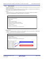
This section describes the contents and selection value displayed on the host PC screen by terminal
software communication.
Refer to the terminal software operating instructions for details on transmitting the MOTOROLA-S
formatted file using the XMODEM communication protocol.
(1) Menu
Select a number from 1 to 8 which corresponds to the number shown in Table 4.2 Processing.
The menu is displayed again if a number other than 1 to 8 is entered.
Terminal software window
M16C/64 User Boot Menu v2.00
1...Blank Check
2...Erase
3...Erase of selection block
4...Program Flash via XModem Download
5...Checksum calculation and CRC calculation
6...Lock of lock bit
7...Display of lock bit status
8...Unlock of lock bit and erase of selection block
>
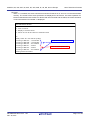
(2) Blank check
When “1” is entered, blocks A, B, and 0 to 3 are checked to see if they are blank (no written data
present). The checked result is displayed for each block.
Terminal software window
5...Checksum calculation and CRC calculation
6...Lock of lock bit
7...Display of lock bit status
8...Unlock of lock bit and erase of selection block
>1
Blank checking user area...
Block-A is a blank.
Block-B is a blank.
Block-0 is a blank.
Block-1 is not a blank.
Block-2 is a blank.
Block-3 is a blank.
Blank check is done.
R01AN0403EJ0102 Rev. 1.02
Dec. 28, 2011
When blocks are blank (no written data present)
When a block is not blank (written data present)
Page 13 of 28
M16C/63, 64, 64A, 64C, 65, 65C, 6C, 5LD, 56D, 5L, 56, 5M, and 57 Groups
Use of User Boot Function
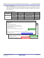
(3) Erase
When “2” is entered, the erase command is executed for blocks A, B, and 0 to 3 in the internal flash
memory. The results of the erase operations are displayed for each block. The erase operation for
blocks locked with the lock bit fails. For blocks that are not locked and are blank, the erase command
is not executed and “Succeeded.” is displayed.
Terminal software window
5...Checksum calculation and CRC calculation
6...Lock of lock bit
7...Display of lock bit status
8...Unlock of lock bit and erase of selection block
>2
Really erase ALL user blocks (Y/N)?y
Erasing of Block-A ... Succeeded.
Erasing of Block-B ... Succeeded.
Erasing of Block-0 ... Succeeded.
Erasing of Block-1 ... Failed.
Erasing of Block-2 ... Failed.
Erasing of Block-3 ... Succeeded.
Erasing all blocks ended.
R01AN0403EJ0102 Rev. 1.02
Dec. 28, 2011
When the erase operation succeeds
When the erase operation fails
Page 14 of 28
Use of User Boot Function
M16C/63, 64, 64A, 64C, 65, 65C, 6C, 5LD, 56D, 5L, 56, 5M, and 57 Groups
(4) Erase of selection block
When “3” is entered, one block selected from blocks A, B, and 0 to 3 of the internal flash memory is
erased. The erase operation for the block locked with the lock bit fails. For a block which is not locked
and is blank, the erase command is not executed and “Succeeded.” is displayed. Table 4.3 lists the
Block Selection Key.
Table 4.3 Block Selection Key
Block Type
Data flash
Program ROM 1
Block Name
Size
Address
Selection Key
Block A
4 KB
E000h to EFFFh
A
Block B
4 KB
F000h to FFFFh
B
Block 3
64 KB
C0000h to CFFFFh
3
Block 2
64 KB
D0000h to DFFFFh
2
Block 1
64 KB
E0000h to EFFFFh
1
Block 0
64 KB
F0000h to FFFFFh
0
Terminal software window
1...Blank Check
2...Erase
3...Erase of selection block
4...Program Flash via XModem Download
5...Checksum calculation and CRC calculation
6...Lock of lock bit
7...Display of lock bit status
8...Unlock of lock bit and erase of selection block
Block selected is block 3.
>3
Please select the block. Choices are 0,1,2,3,A, and B.?3
Erase Block-3 (Y/N)?y
When the erase operation succeeds
Erasing of Block-3 Succeeded.
>3
Please select the block. Choices are 0,1,2,3,A, and B.?1
Erase Block-1 (Y/N)?y
When the erase operation fails
Erasing of Block-1 Failed.
R01AN0403EJ0102 Rev. 1.02
Dec. 28, 2011
Block selected is block 1.
Page 15 of 28
M16C/63, 64, 64A, 64C, 65, 65C, 6C, 5LD, 56D, 5L, 56, 5M, and 57 Groups
Use of User Boot Function
(5) Program transmit file
When “4” is entered, preparations are made to program the internal flash memory. Transmit the file
for programming. Refer to the instructions of the terminal software for communication settings and
transmit operation with the XMODEM protocol. When the internal flash memory to be programmed
(blocks A, B, or 0 to 3) is locked with the lock bit or is not blank, the programming operation fails.
Terminal software window
1...Blank Check
2...Erase
3...Erase of selection block
4...Program Flash via XModem Download
5...Checksum calculation and CRC calculation
6...Lock of lock bit
7...Display of lock bit status
8...Unlock of lock bit and erase of selection block
>4
Program Flash (Y/N)y?
Start XModem download…
Download OK.
When the programming operation succeeds
>4
Program Flash (Y/N)y?
Start XModem download…
Flash program Failed.
When the programming operation fails
(6) Checksum calculation and CRC calculation
When “5” is entered, execute checksum and CRC calculation for blocks A, B, and 0 to 3 of the
internal flash memory. The results of these operations are displayed in 2-byte units for the data flash
(addresses E000h to FFFFh) and program ROM 1 (addresses C0000h to FFFFFh), respectively.
Terminal software window
1...Blank Check
2...Erase
3...Erase of selection block
4...Program Flash via XModem Download
5...Checksum calculation and CRC calculation
6...Lock of lock bit
7...Display of lock bit status
8...Unlock of lock bit and erase of selection block
Checksum value
>5
Sum calculation user area
Data flash... Sum is F000h, Crc is 85F4h
Program ROM... Sum is 0000h, Crc is 8444h
Sum calculation is done.
R01AN0403EJ0102 Rev. 1.02
Dec. 28, 2011
CRC value
Page 16 of 28
M16C/63, 64, 64A, 64C, 65, 65C, 6C, 5LD, 56D, 5L, 56, 5M, and 57 Groups
Use of User Boot Function
(7) Lock of lock bit
When “6” is entered, the lock bit program is executed for blocks A, B, and 0 to 3, and lock bits for
these blocks are set to 0 (locked). The results of the lock bit program are displayed for each block.
For a block whose lock bit is already 0, “Failed.” is displayed.
Terminal software window
5...Checksum calculation and CRC calculation
6...Lock of lock bit
7...Display of lock bit status
8...Unlock of lock bit and erase of selection block
>6
The lock bit is put into the state of the lock.
Lock of Block-A Failed.
When the lock bit program fails
Lock of Block-B Failed.
Lock of Block-0 Succeeded.
Lock of Block-1 Succeeded.
When the lock bit program succeeds
Lock of Block-2 Succeeded.
Lock of Block-3 Succeeded.
Block lock bit program is done.
(8) Display of lock bit status
When “7” is entered, the lock bit status of blocks A, B, and 0 to 3 of the internal flash are read. The
read statuses are displayed for each block.
Terminal software window
5...Checksum calculation and CRC calculation
6...Lock of lock bit
7...Display of lock bit status
8...Unlock of lock bit and erase of selection block
>7
The state of the lock bit is displayed.
Block-A is unlocked.
When blocks are unlocked
Block-B is unlocked.
Block-0 is locked.
Block-1 is locked.
When blocks are locked
Block-2 is locked.
Block-3 is locked.
Read Block lock bit status is done.
R01AN0403EJ0102 Rev. 1.02
Dec. 28, 2011
Page 17 of 28
M16C/63, 64, 64A, 64C, 65, 65C, 6C, 5LD, 56D, 5L, 56, 5M, and 57 Groups
Use of User Boot Function
(9) Unlock of lock bit and erase of selection block
When “8” is entered, the lock bit is disabled (unlocked) and the block selected from blocks A, B, and 0
to 3 of the internal flash memory is erased. In this operation, the lock bit status becomes 1 (unlocked).
For a block which is not locked and is blank, the erase command is not executed and “Succeeded.” is
displayed. Refer to Table 4.3 Block Selection Key for block selection.
Terminal software display
1...Blank Check
2...Erase
3...Erase of selection block
4...Program Flash via XModem Download
5...Checksum calculation and CRC calculation
6...Lock of lock bit
7...Display of lock bit status
8...Unlock of lock bit and erase of selection block
>8
Please select the block. Choices are 0,1,2,3,A, and B.?0
Unlock and erase Block-0 (Y/N)?y
When the unlock and erase
Unlock and erasing of Block-0 Succeeded.
operations succeed
R01AN0403EJ0102 Rev. 1.02
Dec. 28, 2011
Page 18 of 28
M16C/63, 64, 64A, 64C, 65, 65C, 6C, 5LD, 56D, 5L, 56, 5M, and 57 Groups
4.3.2
Use of User Boot Function
Usage Example
Figure 4.1 shows an example of rewriting the internal flash memory using the sample user boot program.
START
Select Menu 1
(Blank check)
Is block blank?
Blank
Not blank
Select Menu 2
(Erase)
Select Menu 4
(Program)
Select Menu 5
(Checksum and CRC
calculation)
Calculation
failed
Checksum
and CRC calculated
successfully?
Calculation
successful
Select Menu 6
(Lock of lock bit)
END
Figure 4.1
Sample User Boot Program
R01AN0403EJ0102 Rev. 1.02
Dec. 28, 2011
Page 19 of 28
M16C/63, 64, 64A, 64C, 65, 65C, 6C, 5LD, 56D, 5L, 56, 5M, and 57 Groups
4.4
Use of User Boot Function
Program
4.4.1
File Composition
Table 4.4 lists the files used in the sample user boot program.
Table 4.4 Files Used in the Sample Program
File Name
Outline
common.c
Common processing module
common.h
Header file for external reference of common processing
module
lowlevelinit.c
MCU initialization module
lowlevelinit.h
Header file for external reference of MCU initialization module
int_dmy.c
Undefined interrupt (dummy) handling
int_dmy.h
Prototype declaration of undefined interrupt handling
flash_drv.c
Internal flash memory programming module in CPU rewrite
mode (EW0 mode)
flash_drv.h
Header file for external reference of internal flash memory
rewriting module
serial0_drv.c
Serial (UART0) data communication module
serial0_drv.h
Header file for external reference of serial (UART0) data
communication module
timerA0_drv.c
Timer A0 (timer mode) control module
timerA0_drv.h
Header file for external reference of timer A0 (timer mode)
control module
timerB5_drv.c
Timer B5 (timer mode) control module
timerB5_drv.h
Header file for external reference of timer B5 (timer mode)
control module
wdtRefresh.h
Macro definition for refreshing watchdog timer
Remarks
Type definition and prototype
declaration of common function
For measuring timeout period
For measuring watchdog timer
refresh cycle
xmodem.c
XMODEM protocol interface module
xmodem.h
Header file for external reference of XMODEM protocol
interface module
flash_menu.c
User boot menu processing module
flash_menu.h
Header file for external reference of user boot menu
processing module
UserBoot.c
User boot main processing
The definition of user boot code
area is included.
Definition of execution address in the RAM area
Definition of relocatable vector,
interrupt handler, executable code
in the RAM area, and data
address in the RAM area
UserBoot.h
R01AN0403EJ0102 Rev. 1.02
Dec. 28, 2011
Usage example of sample source
files
Page 20 of 28
M16C/63, 64, 64A, 64C, 65, 65C, 6C, 5LD, 56D, 5L, 56, 5M, and 57 Groups
4.4.2
Use of User Boot Function
Internal Flash Memory Rewriting Module
Table 4.5 lists Module Interfaces in the internal flash memory rewriting module (flash_drv) of the sample
user boot program, and Table 4.6 lists the definition of data type used in the sample program.
Table 4.5 Module Interfaces
Interface Name
Function
Block index number of internal flash memory
BLOCK_A_IDX
(Block A of data flash)
Block index number of internal flash memory
BLOCK_B_IDX
(Block B of data flash)
Block index number of internal flash memory
BLOCK_0_IDX
(Block 0 of program ROM 1)
Block index number of internal flash memory
BLOCK_1_IDX
(Block 1 of program ROM 1)
Block index number of internal flash memory
BLOCK_2_IDX
(Block 2 of program ROM 1)
Block index number of internal flash memory
BLOCK_3_IDX
(Block 3 of program ROM 1)
FDS_OK
Succeeded
FDS_NOT_BLANK
Not blank
FDS_BLOCK_LOCK
The block lock bit is 0 (locked).
FDS_BLOCK_UNLOCK The block lock bit is 1 (unlocked).
FDS_LBP_FAIL
Lock bit program failed
Program failed
FDS_PROG_FAIL
(A program error notice from the flash memory
has been received.)
Write address error
FDS_ADDR_ERROR
(Not 4-byte aligned)
Erase failed
FDS_ERASE_FAIL
(An erasure error notice from the flash memory
has been received.)
BLOCK_IDX_NUM
BLOCK_FIRST_IDX
LBP_DISABLE
LBP_ENABLE
InitFlashDrv
ClearStatusRegister
BlankReadCheck
BlockBlankCheck
BlockErase
Program128bytes
LockBitProgram
ReadLockBitStatus
FlashReadSumCalc
Number of blocks in flash memory
Remark
FLASH_BLOCK_NUM type data
FLASH_BLOCK_NUM type data
FLASH_BLOCK_NUM type data
FLASH_BLOCK_NUM type data
FLASH_BLOCK_NUM type data
FLASH_BLOCK_NUM type data
FLASH_STATUS type data
FLASH_STATUS type data
FLASH_STATUS type data
FLASH_STATUS type data
FLASH_STATUS type data
FLASH_STATUS type data
FLASH_STATUS type data
FLASH_STATUS type data
Total number of the blocks in data flash
and program ROM 1
Start index of the block definition in the flash
memory
Lock bit disabled
Lock bit enabled
Internal flash memory rewriting module
initialization
Request for clearing the status register of
internal flash memory
Blank check for the specified block (value read in
flash memory is 0xFFFF)
Request for blank (state after erase) check for
the specified block
Request for the auto-erase operation for the
specified block
Request for the 128-byte continuous autoprogram operation
Request for enabling the lock bit of the specified
block
Request for obtaining the lock bit status of the
specified block
Calculation of checksum value and CRC-CCITT
value for the specified block
R01AN0403EJ0102 Rev. 1.02
Dec. 28, 2011
Page 21 of 28
M16C/63, 64, 64A, 64C, 65, 65C, 6C, 5LD, 56D, 5L, 56, 5M, and 57 Groups
Use of User Boot Function
Table 4.6 Definition of Data Type
Data Type Name
Data Type
Definition Header
SBYTE
signed char
common.h
UBYTE
unsigned char
common.h
SWORD
signed short
common.h
UWORD
unsigned short
common.h
SDWORD
signed long
common.h
UDWORD
unsigned long
common.h
FLASH_BLOCK_NUM
enum
flash_drv.h
FLASH_STATUS
enum
flash_drv.h
Functions of flash memory rewriting module (flash_drv) used in the sample user boot program are
described below.
Function
Outline
InitFlashDrv
Initialization of the internal flash memory rewriting module
Interface Name
PRCR
PM10
Content
Definition
Header
sfr64.h
sfr64.h
SFR (Protect register)
SFR (Data flash enable bit)
Standard function (Copy of memory
memcpy
string.h
area)
WDT_INITIALIZE
Watchdog timer refresh
wdtRefresh.h
RAM_DATA_ADDRESS
RAM address to which data copies UserBoot.h
External
Reference RAM_BASED_ROM_DATA_ADDRESS ROM address from which data
UserBoot.h
copies
SIZE_OF_RAM_BASED_ROM_DATA
Number of bytes of copied data
UserBoot.h
RAM address to which program
UserBoot.h
RAM_PROG_ADDRESS
code is copied
ROM address from which program
RAM_BASED_ROM_PROG_ADDRESS
UserBoot.h
code is copied
Number of bytes of copied program
SIZE_OF_RAM_BASED_ROM_PROG
UserBoot.h
code
Declaration void InitFlashDrv (void);
Type
Meaning
Argument
void
None
Type
Meaning
Returned
Value
void
None
Function
• Enable data flash (addresses 0E000h to 0FFFFh).
• Copy the program code for handling the internal flash memory and data to the RAM area.
• Execute watchdog timer refresh processing (refreshing watchdog timer).
Remark
This function must be executed (once) when the function of the internal flash memory rewriting module
(flash_drv) is used.
R01AN0403EJ0102 Rev. 1.02
Dec. 28, 2011
Page 22 of 28
M16C/63, 64, 64A, 64C, 65, 65C, 6C, 5LD, 56D, 5L, 56, 5M, and 57 Groups
Function
Outline
Use of User Boot Function
ClearStatusRegister
Request to clear the status register of internal flash memory
Interface Name
Content
Definition
Header
External
FMR00
sfr64.h
SFR (RY/BY status flag)
Reference
FMR06
SFR (Program status flag)
sfr64.h
FMR07
SFR (Erase status flag)
sfr64.h
Declaration void ClearStatusRegister (void);
Type
Meaning
Argument
void
None
Type
Meaning
Returned
Value
void
None
Function
• Enter CPU rewrite mode (EW0 mode) and execute the software command (clear status register) in the
internal flash memory.
• Exit CPU rewrite mode (EW0 mode) after verifying the status register is cleared.
Remark
Exit this function when the internal flash memory is ready (FMR00 is 1), program status is normal (FMR06
is 0), and the erase status is normal (FMR07 is 0). Interrupts are disabled (I flag is cleared) while in CPU
rewrite mode (EW0 mode).
Function
Outline
BlankReadCheck
Blank check of a specified block (value read in flash memory is 0xFFFF)
Definition
Header
None
None
None
Declaration FLASH_STATUS BlankReadCheck (FLASH_BLOCK_NUM BlockNum, UWORD *Data);
Type
Meaning
The block index number for blank check in the internal
Argument FLASH_BLOCK_NUM
flash memory (value read in flash memory is 0xFFFF)
UWORD *
Value read in flash memory when the block is not blank
Type
Meaning
Returned
FDS_OK: Blank
Value
FLASH_STATUS
FDS_NOT_BLANK: Not blank
Function
• Return FDS_OK (blank) when the data of all specified block areas in the internal flash memory is
0xFFFF.
• Store the read value in the argument *Data when the data of the specified block areas is not 0xFFFF, and
return FDS_NOT_BLANK (not blank).
Remark
None
External
Reference
Interface Name
R01AN0403EJ0102 Rev. 1.02
Dec. 28, 2011
Content
Page 23 of 28
M16C/63, 64, 64A, 64C, 65, 65C, 6C, 5LD, 56D, 5L, 56, 5M, and 57 Groups
Function
Outline
Use of User Boot Function
BlockBlankCheck
Request to blank check (state after erase) the specified block
Interface Name
External
Reference FMR00
Content
Definition
Header
sfr64.h
SFR (RY/BY status flag)
FMR07
SFR (Erase status flag)
sfr64.h
Declaration FLASH_STATUS BlockBlankCheck (FLASH_BLOCK_NUM BlockNum);
Type
Meaning
Argument
The block index number of the specified block for blank
FLASH_BLOCK_NUM
check (state after erase) in the internal flash memory
Type
Meaning
Returned
FDS_OK: Blank
Value
FLASH_STATUS
FDS_NOT_BLANK: Not blank
Function
• Enter CPU rewrite mode (EW0 mode) and execute the software command (block blank check) in the
internal flash memory.
• Determine the returned value depending on the erase status flag (FMR07) and exit CPU rewrite mode
(EW0 mode).
a) Return FDS_OK (blank) when the erase status flag is normal (FMR07 is 0).
b) Return FDS_NOT_BLANK (not blank) when the erase status flag is in error (FMR07 is 1).
Remark
The software command (clear status register) is executed when the returned value is FDS_NOT_BLANK.
Exit this function when the erase status becomes normal (FMR07 is 0) in the internal flash memory.
Interrupts are disabled (I flag is cleared) while in CPU rewrite mode (EW0 mode).
R01AN0403EJ0102 Rev. 1.02
Dec. 28, 2011
Page 24 of 28
M16C/63, 64, 64A, 64C, 65, 65C, 6C, 5LD, 56D, 5L, 56, 5M, and 57 Groups
Function
Outline
Use of User Boot Function
BlockErase
Request for the auto-erase operation for the specified block
Interface Name
Content
Definition
Header
External FMR00
sfr64.h
SFR (RY/BY status flag)
Reference
FMR07
SFR (Erase status flag)
sfr64.h
WDT_INITIALIZE
Refreshing watchdog timer
wdtRefresh.h
Declaration FLASH_STATUS BlockErase (FLASH_BLOCK_NUM BlockNum, UWORD LBPEnableFlag);
Type
Meaning
The block index number for the auto-erase operation in
FLASH_BLOCK_NUM
the internal flash memory
Argument
LBP_ENABLE: Lock bit enabled (FMR02 is 0)
UWORD LBPEnableFlag
LBP_DISABLE: Lock bit disabled (FMR02 is 1)
Type
Meaning
Returned
FDS_OK: Erase succeeded
Value
FLASH_STATUS
FDS_ERASE_FAIL: Erase failed
Function
When the specified block is not blank or is locked while LBPEnableFlag is LBP_ENABLE (lock bit enabled),
the erase command is executed for the block.
When the block is blank and not locked, the erase command is not executed and FDS_OK (erase
succeeded) is returned.
When the specified block is not blank or is locked while LBPEnableFlag is LBP_DISABLE (lock bit
disabled), the lock bit is disabled and the erase command is executed for the block.
When the block is blank and not locked, the erase command is not executed and FDS_OK (erase
succeeded) is returned.
When an erase error or an illegal command error occurs, FDS_ERASE_FAIL (erase failed) is returned as
the returned value.
When the erase operation succeeds, FDS_OK (erase succeeded) is returned.
Remark
The watchdog timer is refreshed during the auto-erase operation (FMR00 is 0) in internal flash memory.
Interrupts are disabled (I flag is cleared) in CPU rewrite mode (EW0 mode).
R01AN0403EJ0102 Rev. 1.02
Dec. 28, 2011
Page 25 of 28
M16C/63, 64, 64A, 64C, 65, 65C, 6C, 5LD, 56D, 5L, 56, 5M, and 57 Groups
Function
Outline
Use of User Boot Function
Program128bytes
Request for 128-byte continuous auto-program operation
Interface Name
Content
External
Reference FMR00
Definition
Header
sfr64.h
SFR (RY/BY status flag)
FMR06
SFR (Program status flag)
sfr64.h
Declaration FLASH_STATUS Program128bytes (UDWORD Address, UWORD *Data);
Type
Meaning
UDWORD
Start address to program in the internal flash memory
Argument
Buffer pointer for storing data to be programmed (128
UWORD *
bytes)
Type
Meaning
Returned
FDS_OK: Program succeeded
Value
FLASH_STATUS
FDS_PROG_FAIL: Program failed
FDS_ADDR_ERROR: Write address error
Function
• When the start address for programming (UDWORD Address) is not 4-byte aligned, set FDS_ADDR_ERROR
(write address error) as the returned value and terminate the operation.
• When the start address for programming (UDWORD Address) is 4-byte aligned, enter CPU rewrite mode
(EW0 mode) and execute the software command (program) for 128-byte data in the internal flash
memory.
• Determine the returned value depending on the program status flag (FMR06) and exit CPU rewrite mode
(EW0 mode).
a) Return FDS_OK (program succeeded) when the program status flag is normal (FMR06 is 0).
b) Return FDS_PROG_FAIL (program failed) when program status flag is in error (FMR06 is 1).
Remark
Interrupts are disabled (I flag is cleared) while in CPU rewrite mode (EW0 mode).
Function
Outline
LockBitProgram
Request to enable the lock bit of the specified block
Interface Name
Content
Definition
Header
sfr64.h
sfr64.h
External
Reference FMR00
SFR (RY/BY status flag)
FMR06
SFR (Program status flag)
Declaration FLASH_STATUS LockBitProgram (FLASH_BLOCK_NUM BlockNum);
Type
Meaning
Argument
The block index number of the specified block for the
FLASH_BLOCK_NUM
lock bit program in the internal flash memory
Type
Meaning
Returned
FDS_OK: Lock bit program succeeded
Value
FLASH_STATUS
FDS_LBP_FAIL: Lock bit program failed
Function
• Enter CPU rewrite mode (EW0 mode) and execute the software command (lock bit program) in the
internal flash memory.
• Determine the returned value depending on the program status flag (FMR06) and exit CPU rewrite mode
(EW0 mode).
a) Return FDS_OK (lock bit program succeeded) when program status flag is normal (FMR06 is 0).
b) Return FDS_LBP_FAIL (lock bit program failed) when program status flag is in error (FMR06 is 1).
Remark
Interrupts are disabled (I flag is cleared) in CPU rewrite mode (EW0 mode).
R01AN0403EJ0102 Rev. 1.02
Dec. 28, 2011
Page 26 of 28
M16C/63, 64, 64A, 64C, 65, 65C, 6C, 5LD, 56D, 5L, 56, 5M, and 57 Groups
Name
Outline
Use of User Boot Function
ReadLockBitStatus
Request to obtain the lock bit status of the specified block
Interface Name
Content
External
Reference FMR00
Definition
Header
sfr64.h
SFR (RY/BY status flag)
FMR16
SFR (Lock bit status flag)
sfr64.h
Declaration FLASH_STATUS ReadLockBitStatus (FLASH_BLOCK_NUM BlockNum);
Type
Meaning
Argument
The block index number for obtaining the lock bit status
FLASH_BLOCK_NUM
in the internal flash memory
Type
Meaning
Returned
FDS_BLOCK_LOCK: The lock bit status is 0 (locked)
Value
FLASH_STATUS
FDS_BLOCK_UNLOCK: The lock bit status is 1 (unlocked)
Function
• Enter CPU rewrite mode (EW0 mode) and execute the software command (read lock bit status) in the
internal flash memory.
• Determine the returned value depending on the lock bit status (FMR16) and exit CPU rewrite mode (EW0
mode).
a) Return FDS_BLOCK_LOCK (locked) when the lock bit status is normal (FMR16 is 0).
b) Return FDS_BLOCK_UNLOCK (unlocked) when the lock bit status is in error (FMR16 is 1).
Remark
Interrupts are disabled (I flag is cleared) while in CPU rewrite mode (EW0 mode).
Name
Outline
FlashReadSumCalc
Calculation of checksum value and CRC-CCITT value for the specified block
Definition
Interface Name
Content
Header
External
Reference CRCD
SFR (CRC data register)
sfr64.h
CRCIN
SFR (CRC input register)
sfr64.h
void FlashReadSumCalc (FLASH_BLOCK_NUM BlockNum, UWORD *SumValue, UWORD
Declaration
*CrcValue);
Type
Meaning
The block index number for checksum and CRC
FLASH_BLOCK_NUM
calculation in the internal flash memory
Argument
UWORD *
Buffer pointer for the checksum value
UWORD *
Buffer pointer for the CRC value
Type
Meaning
Returned
Value
void
None
Function
Read data of all specified block areas in the internal flash memory and calculate their checksum values
and CRC values.
Remark
The checksum value (UWORD *SumValue) and the CRC value (UWORD *CrcValue) should be initialized
before this function is called.
R01AN0403EJ0102 Rev. 1.02
Dec. 28, 2011
Page 27 of 28
M16C/63, 64, 64A, 64C, 65, 65C, 6C, 5LD, 56D, 5L, 56, 5M, and 57 Groups
5.
Use of User Boot Function
Sample Code
Sample code can be downloaded from the Renesas Electronics website.
6.
Reference Documents
M16C/63 Group User’s Manual: Hardware Rev.2.00
M16C/64 Group User’s Manual: Hardware Rev.1.05
M16C/64A Group User’s Manual: Hardware Rev.2.00
M16C/64C Group User’s Manual: Hardware Rev.1.00
M16C/65 Group User’s Manual: Hardware Rev.2.00
M16C/65C Group User’s Manual: Hardware Rev.1.00
M16C/6C Group User’s Manual: Hardware Rev.2.00
M16C/5LD Group, M16C/56D Group User’s Manual: Hardware Rev.1.20
M16C/5L Group, M16C/56 Group User’s Manual: Hardware Rev.1.10
M16C/5M Group, M16C/57 Group User’s Manual: Hardware Rev.1.10
The latest versions can be downloaded from the Renesas Electronics website.
Technical Update/Technical News
The latest information can be downloaded from the Renesas Electronics website.
C Compiler Manual
M16C Series, R8C Family C Compiler Package V.5.45
C Compiler User’s Manual Rev.2.00
The latest version can be downloaded from the Renesas Electronics website.
Website and Support
Renesas Electronics website
http://www.renesas.com/
Inquiries
http://www.renesas.com/inquiry
R01AN0403EJ0102 Rev. 1.02
Dec. 28, 2011
Page 28 of 28
M16C/63, 64, 64A, 64C, 65, 65C, 6C, 5LD, 56D, 5L, 56,
5M, and 57 Groups
Use of User Boot Function
Revision History
Description
Rev.
Date
1.00
Jan. 22, 2010
—
1.01
Feb. 28. 2011
—
1.02
Dec. 28. 2011
1
1. Abstract: Added the sentence “This application note describes the
user boot function using the M16C/64 Group”.
2
3.1 Outline: Added.
2
3.2 Introduction of User Boot Function: Rewrote the second bullet.
9
Figure 3.5 Processing of User Boot Mode Selection: Changed “Lowvoltage detect reset” to “Voltage monitor reset”.
12
4.3 Processing Outline: Revised.
20
Table 4.4 Files Used in the Sample Program: Modified the Outlines for
xmodem.c and xmodem.h.
21
Table 4.5 Module Interfaces:
• Modified the Remarks from FDS_OK to FDS_ERASE_FAIL.
• Added interfaces LBP_DISABLE and LBP_ENABLE.
• Modified the Function for FlashReadSumCalc.
25
BlockErase function table:
• Added arguments LBP_ENABLE and LBP_DISABLE.
• Modified the Function.
27
FlashReadSumCalc function table: Modified the Outline.
Page
Summary
First edition issued
Add: M16C/63, M16C/64C, M16C/65C, M16C/6C, M16C/5LD,
M16C/56D, M16C/5L, M16C/56, M16C/5M, and M16C/57
All trademarks and registered trademarks are the property of their respective owners.
A-1
General Precautions in the Handling of MPU/MCU Products
The following usage notes are applicable to all MPU/MCU products from Renesas. For detailed usage notes
on the products covered by this manual, refer to the relevant sections of the manual. If the descriptions under
General Precautions in the Handling of MPU/MCU Products and in the body of the manual differ from each
other, the description in the body of the manual takes precedence.
1. Handling of Unused Pins
Handle unused pins in accord with the directions given under Handling of Unused Pins in the
manual.
The input pins of CMOS products are generally in the high-impedance state. In operation
with an unused pin in the open-circuit state, extra electromagnetic noise is induced in the
vicinity of LSI, an associated shoot-through current flows internally, and malfunctions occur
due to the false recognition of the pin state as an input signal become possible. Unused
pins should be handled as described under Handling of Unused Pins in the manual.
2. Processing at Power-on
The state of the product is undefined at the moment when power is supplied.
The states of internal circuits in the LSI are indeterminate and the states of register
settings and pins are undefined at the moment when power is supplied.
In a finished product where the reset signal is applied to the external reset pin, the states
of pins are not guaranteed from the moment when power is supplied until the reset
process is completed.
In a similar way, the states of pins in a product that is reset by an on-chip power-on reset
function are not guaranteed from the moment when power is supplied until the power
reaches the level at which resetting has been specified.
3. Prohibition of Access to Reserved Addresses
Access to reserved addresses is prohibited.
The reserved addresses are provided for the possible future expansion of functions. Do
not access these addresses; the correct operation of LSI is not guaranteed if they are
accessed.
4. Clock Signals
After applying a reset, only release the reset line after the operating clock signal has become
stable. When switching the clock signal during program execution, wait until the target clock
signal has stabilized.
When the clock signal is generated with an external resonator (or from an external
oscillator) during a reset, ensure that the reset line is only released after full stabilization of
the clock signal. Moreover, when switching to a clock signal produced with an external
resonator (or by an external oscillator) while program execution is in progress, wait until
the target clock signal is stable.
5. Differences between Products
Before changing from one product to another, i.e. to one with a different part number, confirm
that the change will not lead to problems.
The characteristics of MPU/MCU in the same group but having different part numbers may
differ because of the differences in internal memory capacity and layout pattern. When
changing to products of different part numbers, implement a system-evaluation test for
each of the products.
Notice
1.
All information included in this document is current as of the date this document is issued. Such information, however, is subject to change without any prior notice. Before purchasing or using any Renesas
Electronics products listed herein, please confirm the latest product information with a Renesas Electronics sales office. Also, please pay regular and careful attention to additional and different information to
be disclosed by Renesas Electronics such as that disclosed through our website.
2.
Renesas Electronics does not assume any liability for infringement of patents, copyrights, or other intellectual property rights of third parties by or arising from the use of Renesas Electronics products or
technical information described in this document. No license, express, implied or otherwise, is granted hereby under any patents, copyrights or other intellectual property rights of Renesas Electronics or
others.
3.
You should not alter, modify, copy, or otherwise misappropriate any Renesas Electronics product, whether in whole or in part.
4.
Descriptions of circuits, software and other related information in this document are provided only to illustrate the operation of semiconductor products and application examples. You are fully responsible for
the incorporation of these circuits, software, and information in the design of your equipment. Renesas Electronics assumes no responsibility for any losses incurred by you or third parties arising from the
use of these circuits, software, or information.
5.
When exporting the products or technology described in this document, you should comply with the applicable export control laws and regulations and follow the procedures required by such laws and
regulations. You should not use Renesas Electronics products or the technology described in this document for any purpose relating to military applications or use by the military, including but not limited to
the development of weapons of mass destruction. Renesas Electronics products and technology may not be used for or incorporated into any products or systems whose manufacture, use, or sale is
prohibited under any applicable domestic or foreign laws or regulations.
6.
Renesas Electronics has used reasonable care in preparing the information included in this document, but Renesas Electronics does not warrant that such information is error free. Renesas Electronics
7.
Renesas Electronics products are classified according to the following three quality grades: "Standard", "High Quality", and "Specific". The recommended applications for each Renesas Electronics product
assumes no liability whatsoever for any damages incurred by you resulting from errors in or omissions from the information included herein.
depends on the product's quality grade, as indicated below. You must check the quality grade of each Renesas Electronics product before using it in a particular application. You may not use any Renesas
Electronics product for any application categorized as "Specific" without the prior written consent of Renesas Electronics. Further, you may not use any Renesas Electronics product for any application for
which it is not intended without the prior written consent of Renesas Electronics. Renesas Electronics shall not be in any way liable for any damages or losses incurred by you or third parties arising from the
use of any Renesas Electronics product for an application categorized as "Specific" or for which the product is not intended where you have failed to obtain the prior written consent of Renesas Electronics.
The quality grade of each Renesas Electronics product is "Standard" unless otherwise expressly specified in a Renesas Electronics data sheets or data books, etc.
"Standard":
Computers; office equipment; communications equipment; test and measurement equipment; audio and visual equipment; home electronic appliances; machine tools;
personal electronic equipment; and industrial robots.
"High Quality": Transportation equipment (automobiles, trains, ships, etc.); traffic control systems; anti-disaster systems; anti-crime systems; safety equipment; and medical equipment not specifically
designed for life support.
"Specific":
Aircraft; aerospace equipment; submersible repeaters; nuclear reactor control systems; medical equipment or systems for life support (e.g. artificial life support devices or systems), surgical
implantations, or healthcare intervention (e.g. excision, etc.), and any other applications or purposes that pose a direct threat to human life.
8.
You should use the Renesas Electronics products described in this document within the range specified by Renesas Electronics, especially with respect to the maximum rating, operating supply voltage
range, movement power voltage range, heat radiation characteristics, installation and other product characteristics. Renesas Electronics shall have no liability for malfunctions or damages arising out of the
use of Renesas Electronics products beyond such specified ranges.
9.
Although Renesas Electronics endeavors to improve the quality and reliability of its products, semiconductor products have specific characteristics such as the occurrence of failure at a certain rate and
malfunctions under certain use conditions. Further, Renesas Electronics products are not subject to radiation resistance design. Please be sure to implement safety measures to guard them against the
possibility of physical injury, and injury or damage caused by fire in the event of the failure of a Renesas Electronics product, such as safety design for hardware and software including but not limited to
redundancy, fire control and malfunction prevention, appropriate treatment for aging degradation or any other appropriate measures. Because the evaluation of microcomputer software alone is very difficult,
please evaluate the safety of the final products or system manufactured by you.
10. Please contact a Renesas Electronics sales office for details as to environmental matters such as the environmental compatibility of each Renesas Electronics product. Please use Renesas Electronics
products in compliance with all applicable laws and regulations that regulate the inclusion or use of controlled substances, including without limitation, the EU RoHS Directive. Renesas Electronics assumes
no liability for damages or losses occurring as a result of your noncompliance with applicable laws and regulations.
11. This document may not be reproduced or duplicated, in any form, in whole or in part, without prior written consent of Renesas Electronics.
12. Please contact a Renesas Electronics sales office if you have any questions regarding the information contained in this document or Renesas Electronics products, or if you have any other inquiries.
(Note 1)
"Renesas Electronics" as used in this document means Renesas Electronics Corporation and also includes its majority-owned subsidiaries.
(Note 2)
"Renesas Electronics product(s)" means any product developed or manufactured by or for Renesas Electronics.
http://www.renesas.com
SALES OFFICES
Refer to "http://www.renesas.com/" for the latest and detailed information.
Renesas Electronics America Inc.
2880 Scott Boulevard Santa Clara, CA 95050-2554, U.S.A.
Tel: +1-408-588-6000, Fax: +1-408-588-6130
Renesas Electronics Canada Limited
1101 Nicholson Road, Newmarket, Ontario L3Y 9C3, Canada
Tel: +1-905-898-5441, Fax: +1-905-898-3220
Renesas Electronics Europe Limited
Dukes Meadow, Millboard Road, Bourne End, Buckinghamshire, SL8 5FH, U.K
Tel: +44-1628-585-100, Fax: +44-1628-585-900
Renesas Electronics Europe GmbH
Arcadiastrasse 10, 40472 Düsseldorf, Germany
Tel: +49-211-65030, Fax: +49-211-6503-1327
Renesas Electronics (China) Co., Ltd.
7th Floor, Quantum Plaza, No.27 ZhiChunLu Haidian District, Beijing 100083, P.R.China
Tel: +86-10-8235-1155, Fax: +86-10-8235-7679
Renesas Electronics (Shanghai) Co., Ltd.
Unit 204, 205, AZIA Center, No.1233 Lujiazui Ring Rd., Pudong District, Shanghai 200120, China
Tel: +86-21-5877-1818, Fax: +86-21-6887-7858 / -7898
Renesas Electronics Hong Kong Limited
Unit 1601-1613, 16/F., Tower 2, Grand Century Place, 193 Prince Edward Road West, Mongkok, Kowloon, Hong Kong
Tel: +852-2886-9318, Fax: +852 2886-9022/9044
Renesas Electronics Taiwan Co., Ltd.
13F, No. 363, Fu Shing North Road, Taipei, Taiwan
Tel: +886-2-8175-9600, Fax: +886 2-8175-9670
Renesas Electronics Singapore Pte. Ltd.
1 harbourFront Avenue, #06-10, keppel Bay Tower, Singapore 098632
Tel: +65-6213-0200, Fax: +65-6278-8001
Renesas Electronics Malaysia Sdn.Bhd.
Unit 906, Block B, Menara Amcorp, Amcorp Trade Centre, No. 18, Jln Persiaran Barat, 46050 Petaling Jaya, Selangor Darul Ehsan, Malaysia
Tel: +60-3-7955-9390, Fax: +60-3-7955-9510
Renesas Electronics Korea Co., Ltd.
11F., Samik Lavied' or Bldg., 720-2 Yeoksam-Dong, Kangnam-Ku, Seoul 135-080, Korea
Tel: +82-2-558-3737, Fax: +82-2-558-5141
© 2011 Renesas Electronics Corporation. All rights reserved.
Colophon 1.1