1
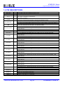
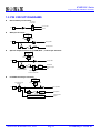
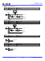
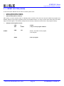
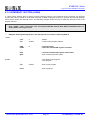
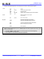
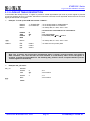
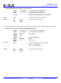
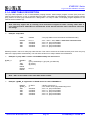
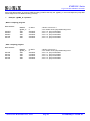
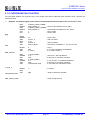
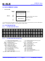
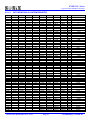
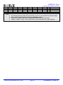
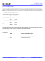
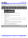
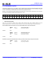
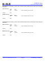
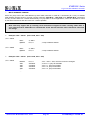
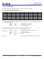
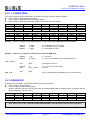
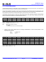
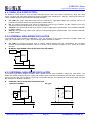
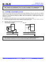
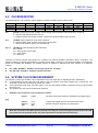
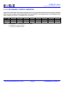
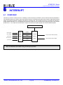
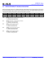
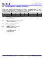
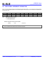
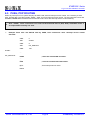
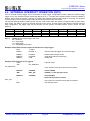
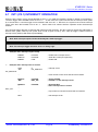
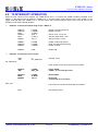
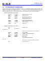
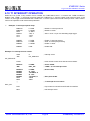
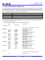
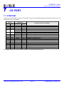
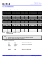
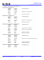
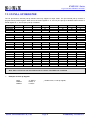
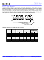
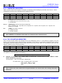
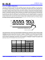
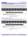
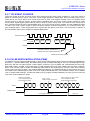
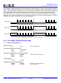
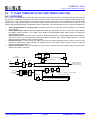
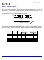
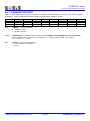
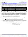
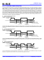
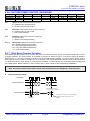
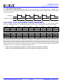
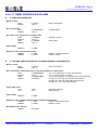
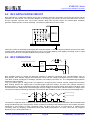
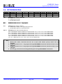
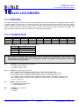
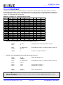
SN8P2318 Series C-type LCD, RFC 8-Bit Micro-Controller 10 4x32 LCD DRIVER 10.1 OVERVIEW The LCD driver density is 4x32 (4 commons and 32 segments, 128 dots) and builds in C-type and R-type structure. The LCD supports 1/4 duty and 1/2, 1/3 bias LCD panel. The LCD frame rate is 64Hz and clock source is external 32768Hz oscillator crystal or RC type. The C-type only supports 1/3 bias LCD structure. R-type is using external bias circuit to adjust LCD power and bias voltage. There are 16-pin GPIO shared with SEGs controlled by register. For difference density LCD panel, users can decides more GPIO pins for application. 10.2 LCD REGISTERS 0CBH LCDM Read/Write After reset Bit [7:6] Bit 7 CPCK1 R/W 0 Bit 6 CPCK0 R/W 0 Bit 5 VLCDCP R/W 0 Bit 4 PSEG2 R/W 0 Bit 3 PSEG1 R/W 0 Bit 2 PSEG0 R/W 0 Bit 1 BIAS R/W 0 Bit 0 LCDENB R/W 0 CPCK[1:0]: VLCD charge-pump clock selection. CPCK[1:0] Charge-pump Clock 00 32KHz 01 16KHz 10 4KHz 11 1KHz Note: In general speaking, 1KHz charge-pump clock is enough for most application. Lower charge-pump clock frequency can save more power consumption. Higher charge-pump clock frequency can provide stronger VLCD driving capability. Bit 5 VLCDCP: VLCD charge-pump control bit. 0 = Disable. LCD is R-type. 1 = Enable. LCD is C-type. Bit [4:2] PSEG2: LCD shared pin control bit. 000 = Disable all LCD shared pins’ GPIO function. The SEG pin number is 32. 001 = Enable P2.0~P2.3 (SEG28~SEG31) GPIO function. The SEG pin number is 28. 010 = Enable P2.0~P2.7 (SEG24~SEG31) GPIO function. The SEG pin number is 24. 011 = Enable P2.0~P2.7 and P3.0~P3.3 (SEG20~31) GPIO function. The SEG pin number is 20. 100 = Enable P2.0~P2.7 and P3.0~P3.7 (SEG16~31) GPIO function. The SEG pin number is 16. 101~111 = Reserved. Bit 1 BIAS: LCD bias control bit. 0 = 1/3 bias (C type and R type). 1 = 1/2 bias (R type only). Bit 0 LCDENB: LCD control bit. 0 = Disable. 1 = Enable. SONiX TECHNOLOGY CO., LTD Page 102 Preliminary Version 0.1