1
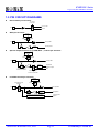
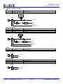
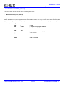
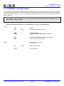
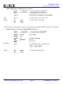
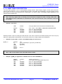
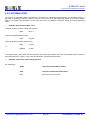
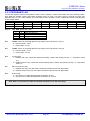
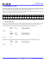
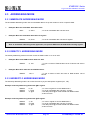
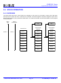
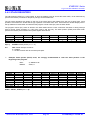
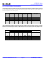
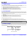
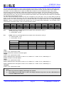
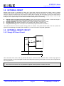
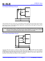
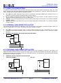
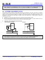
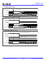
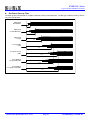
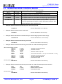
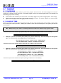
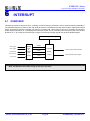
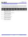
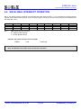
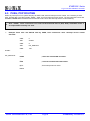
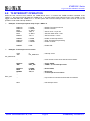
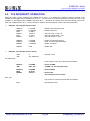
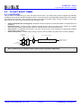
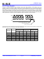
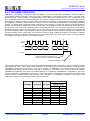
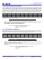
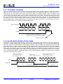
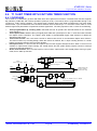
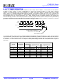
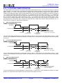
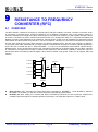
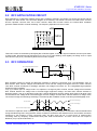
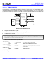
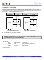
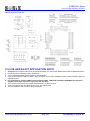
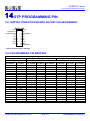
SN8P2318 Series C-type LCD, RFC 8-Bit Micro-Controller 3.9.2 Diode & RC Reset Circuit VDD R1 47K ohm DIODE R2 RST MCU 100 ohm C1 0.1uF VSS VCC GND This is the better reset circuit. The R1 and C1 circuit operation is like the simply reset circuit to make a power on signal. The reset circuit has a simply protection against unusual power. The diode offers a power positive path to conduct higher power to VDD. It is can make reset pin voltage level to synchronize with VDD voltage. The structure can improve slight brown out reset condition. Note: The R2 100 ohm resistor of “Simply reset circuit” and “Diode & RC reset circuit” is necessary to limit any current flowing into reset pin from external capacitor C in the event of reset pin breakdown due to Electrostatic Discharge (ESD) or Electrical Over-stress (EOS). 3.9.3 Zener Diode Reset Circuit VDD R1 33K ohm E R2 B 10K ohm Vz Q1 C RST MCU R3 40K ohm VSS VCC GND The zener diode reset circuit is a simple low voltage detector and can improve brown out reset condition completely. Use zener voltage to be the active level. When VDD voltage level is above “Vz + 0.7V”, the C terminal of the PNP transistor outputs high voltage and MCU operates normally. When VDD is below “Vz + 0.7V”, the C terminal of the PNP transistor outputs low voltage and MCU is in reset mode. Decide the reset detect voltage by zener specification. Select the right zener voltage to conform the application. SONiX TECHNOLOGY CO., LTD Page 44 Preliminary Version 0.1