Download SN8P2318
Transcript
SN8P2318 Series C-type LCD, RFC 8-Bit Micro-Controller SN8P2318 Series USER’S MANUAL Preliminary Version 0.1 SN8P2318 SONiX 8-Bit Micro-Controller SONIX reserves the right to make change without further notice to any products herein to improve reliability, function or design. SONIX does not assume any liability arising out of the application or use of any product or circuit described herein; neither does it convey any license under its patent rights nor the rights of others. SONIX products are not designed, intended, or authorized for us as components in systems intended, for surgical implant into the body, or other applications intended to support or sustain life, or for any other application in which the failure of the SONIX product could create a situation where personal injury or death may occur. Should Buyer purchase or use SONIX products for any such unintended or unauthorized application. Buyer shall indemnify and hold SONIX and its officers, employees, subsidiaries, affiliates and distributors harmless against all claims, cost, damages, and expenses, and reasonable attorney fees arising out of, directly or indirectly, any claim of personal injury or death associated with such unintended or unauthorized use even if such claim alleges that SONIX was negligent regarding the design or manufacture of the part. SONiX TECHNOLOGY CO., LTD Page 1 Preliminary Version 0.1 SN8P2318 Series C-type LCD, RFC 8-Bit Micro-Controller AMENDENT HISTORY Version VER 0.1 Date Mar. 2010 Description First issue. SONiX TECHNOLOGY CO., LTD Page 2 Preliminary Version 0.1 SN8P2318 Series C-type LCD, RFC 8-Bit Micro-Controller Table of Content AMENDENT HISTORY ................................................................................................................................ 2 11 PRODUCT OVERVIEW ........................................................................................................................... 8 1.1 1.2 1.3 1.4 1.5 22 FEATURES ........................................................................................................................................ 8 SYSTEM BLOCK DIAGRAM .......................................................................................................... 9 PIN ASSIGNMENT ........................................................................................................................... 9 PIN DESCRIPTIONS ....................................................................................................................... 10 PIN CIRCUIT DIAGRAMS ............................................................................................................. 11 CENTRAL PROCESSOR UNIT (CPU) .................................................................................................. 13 2.1 PROGRAM MEMORY (ROM) ....................................................................................................... 13 2.1.1 RESET VECTOR (0000H) ...................................................................................................... 14 2.1.2 INTERRUPT VECTOR (0008H) ............................................................................................. 15 2.1.3 LOOK-UP TABLE DESCRIPTION ........................................................................................ 17 2.1.4 JUMP TABLE DESCRIPTION ............................................................................................... 19 2.1.5 CHECKSUM CALCULATION............................................................................................... 21 2.2 DATA MEMORY (RAM) ................................................................................................................ 22 2.2.1 SYSTEM REGISTER .............................................................................................................. 22 2.2.1.1 SYSTEM REGISTER TABLE ............................................................................................ 22 2.2.1.2 SYSTEM REGISTER DESCRIPTION ............................................................................... 22 2.2.1.3 BIT DEFINITION of SYSTEM REGISTER ....................................................................... 23 2.2.2 ACCUMULATOR ................................................................................................................... 25 2.2.3 PROGRAM FLAG ................................................................................................................... 26 2.2.4 PROGRAM COUNTER........................................................................................................... 27 2.2.5 H, L REGISTERS..................................................................................................................... 30 2.2.6 Y, Z REGISTERS..................................................................................................................... 31 2.2.7 R REGISTER ........................................................................................................................... 31 2.3 ADDRESSING MODE .................................................................................................................... 32 2.3.1 IMMEDIATE ADDRESSING MODE .................................................................................... 32 2.3.2 DIRECTLY ADDRESSING MODE ....................................................................................... 32 2.3.3 INDIRECTLY ADDRESSING MODE ................................................................................... 32 2.4 STACK OPERATION ...................................................................................................................... 33 2.4.1 OVERVIEW ............................................................................................................................. 33 2.4.2 STACK REGISTERS ............................................................................................................... 34 2.4.3 STACK OPERATION EXAMPLE.......................................................................................... 35 2.5 CODE OPTION TABLE .................................................................................................................. 36 2.5.1 High_Clk code option ............................................................................................................... 36 SONiX TECHNOLOGY CO., LTD Page 3 Preliminary Version 0.1 SN8P2318 Series C-type LCD, RFC 8-Bit Micro-Controller 33 2.5.2 Low_Clk code option ............................................................................................................... 36 2.5.3 2.5.4 2.5.5 2.5.6 Fcpu code option ...................................................................................................................... 36 Reset_Pin code option .............................................................................................................. 37 Security code option ................................................................................................................. 37 Noise Filter code option ........................................................................................................... 37 RESET ...................................................................................................................................................... 38 3.1 3.2 3.3 3.4 OVERVIEW ..................................................................................................................................... 38 POWER ON RESET......................................................................................................................... 39 WATCHDOG RESET ...................................................................................................................... 39 BROWN OUT RESET ..................................................................................................................... 39 3.5 THE SYSTEM OPERATING VOLTAGE ....................................................................................... 40 3.6 LOW VOLTAGE DETECTOR (LVD) ............................................................................................ 40 3.7 BROWN OUT RESET IMPROVEMENT ....................................................................................... 42 3.8 EXTERNAL RESET ........................................................................................................................ 43 3.9 EXTERNAL RESET CIRCUIT ....................................................................................................... 43 3.9.1 Simply RC Reset Circuit .......................................................................................................... 43 3.9.2 Diode & RC Reset Circuit ........................................................................................................ 44 3.9.3 Zener Diode Reset Circuit ........................................................................................................ 44 3.9.4 Voltage Bias Reset Circuit ....................................................................................................... 45 3.9.5 External Reset IC ...................................................................................................................... 45 44 SYSTEM CLOCK .................................................................................................................................... 46 4.1 OVERVIEW ..................................................................................................................................... 46 4.2 FCPU (INSTRUCTION CYCLE) ...................................................................................................... 46 4.3 SYSTEM HIGH-SPEED CLOCK .................................................................................................... 46 4.3.1 HIGH_CLK CODE OPTION ................................................................................................... 47 4.3.2 INTERNAL HIGH-SPEED OSCILLATOR ............................................................................ 47 4.3.3 EXTERNAL HIGH-SPEED OSCILLATOR ........................................................................... 47 4.4 SYSTEM LOW-SPEED CLOCK ..................................................................................................... 48 4.5 OSCM REGISTER ........................................................................................................................... 49 4.6 4.7 55 SYSTEM CLOCK MEASUREMENT ............................................................................................. 49 SYSTEM CLOCK TIMING ............................................................................................................. 50 SYSTEM OPERATION MODE .............................................................................................................. 53 5.1 5.2 5.3 5.4 5.5 5.6 OVERVIEW ..................................................................................................................................... 53 NORMAL MODE ............................................................................................................................ 54 SLOW MODE .................................................................................................................................. 54 POWER DOWN MDOE .................................................................................................................. 54 GREEN MODE ................................................................................................................................ 55 OPERATING MODE CONTROL MACRO .................................................................................... 56 SONiX TECHNOLOGY CO., LTD Page 4 Preliminary Version 0.1 SN8P2318 Series C-type LCD, RFC 8-Bit Micro-Controller 5.7 5.7.1 5.7.2 5.7.3 66 77 88 WAKEUP ......................................................................................................................................... 57 OVERVIEW ............................................................................................................................. 57 WAKEUP TIME ...................................................................................................................... 57 P1W WAKEUP CONTROL REGISTER ................................................................................ 59 INTERRUPT ............................................................................................................................................ 60 6.1 6.2 6.3 6.4 6.5 OVERVIEW ..................................................................................................................................... 60 INTEN INTERRUPT ENABLE REGISTER ................................................................................... 61 INTRQ INTERRUPT REQUEST REGISTER ................................................................................ 62 GIE GLOBAL INTERRUPT OPERATION .................................................................................... 63 PUSH, POP ROUTINE..................................................................................................................... 64 6.6 6.7 6.8 6.9 6.10 6.11 EXTERNAL INTERRUPT OPERATION (INT0) ........................................................................... 65 INT1 (P0.1) INTERRUPT OPERATION ......................................................................................... 66 T0 INTERRUPT OPERATION........................................................................................................ 67 TC0 INTERRUPT OPERATION ..................................................................................................... 68 T1 INTERRUPT OPERATION........................................................................................................ 69 MULTI-INTERRUPT OPERATION ............................................................................................... 70 I/O PORT .................................................................................................................................................. 71 7.1 7.2 OVERVIEW ..................................................................................................................................... 71 I/O PORT MODE ............................................................................................................................. 72 7.3 7.4 I/O PULL UP REGISTER ................................................................................................................ 74 I/O PORT DATA REGISTER .......................................................................................................... 75 TIMERS.................................................................................................................................................... 76 8.1 WATCHDOG TIMER ...................................................................................................................... 76 8.2 T0 8-BIT BASIC TIMER ........................................................................................................................ 78 8.2.1 OVERVIEW ............................................................................................................................. 78 8.2.2 T0 Timer Operation .................................................................................................................. 79 8.2.3 T0M MODE REGISTER ......................................................................................................... 80 8.2.4 T0C COUNTING REGISTER ................................................................................................. 80 8.2.5 T0 TIMER OPERATION EXPLAME ..................................................................................... 81 8.3 TC0 8-BIT TIMER/COUNTER ....................................................................................................... 82 8.3.1 OVERVIEW ............................................................................................................................. 82 8.3.2 TC0 TIMER OPERATION ...................................................................................................... 83 8.3.3 TC0M MODE REGISTER ....................................................................................................... 84 8.3.4 TC0C COUNTING REGISTER .............................................................................................. 84 8.3.5 TC0R AUTO-RELOAD REGISTER ....................................................................................... 85 8.3.6 TC0D PWM DUTY REGISTER ............................................................................................. 85 8.3.7 TC0 EVENT COUNTER ......................................................................................................... 86 8.3.8 PULSE WIDTH MODULATION (PWM) .............................................................................. 86 SONiX TECHNOLOGY CO., LTD Page 5 Preliminary Version 0.1 SN8P2318 Series C-type LCD, RFC 8-Bit Micro-Controller 8.3.9 TC0 TIMER OPERATION EXPLAME .................................................................................. 87 8.4 T1 16-BIT TIMER WITH CAPTURE TIMER FUNCTION .......................................................................... 89 8.4.1 OVERVIEW ............................................................................................................................. 89 8.4.2 T1 TIMER OPERATION ......................................................................................................... 90 8.4.3 T1M MODE REGISTER ......................................................................................................... 91 8.4.4 T1CH, T1CL 16-bit COUNTING REGISTERS ...................................................................... 92 8.4.5 T1 CPATURE TIMER OPERATION ..................................................................................... 93 8.4.6 CAPTURE TIMER CONTROL REGISTERS ........................................................................ 94 8.4.7 10-bit Event Counter Function ................................................................................................. 94 8.4.8 T1VCH, T1VCL 10-bit EVENT COUNTER REGISTERS .................................................... 95 8.4.9 T1 TIMER OPERATION EXPLAME ..................................................................................... 96 99 RESISTANCE TO FREQURNCY CONVERTER (RFC) ...................................................................... 98 9.1 9.2 9.3 9.4 9.5 1100 OVERVIEW ..................................................................................................................................... 98 RFC APPLICATION CIRCUIT ....................................................................................................... 99 RFC OPERATION ........................................................................................................................... 99 RFCM REGISTER ......................................................................................................................... 100 RFC OPERATION EXPLAME...................................................................................................... 101 4X32 LCD DRIVER .......................................................................................................................... 102 10.1 OVERVIEW ................................................................................................................................... 102 10.2 10.3 10.4 10.5 10.6 LCD REGISTERS .......................................................................................................................... 102 C-TYPE LCD MODE ..................................................................................................................... 103 R-TYPE LCD MODE ..................................................................................................................... 104 LCD RAM MAP ............................................................................................................................. 105 LCD WAVEFORM ........................................................................................................................ 106 1111 INSTRUCTION TABLE .................................................................................................................... 107 1122 ELECTRICAL CHARACTERISTIC................................................................................................. 108 12.1 12.2 1133 ABSOLUTE MAXIMUM RATING .............................................................................................. 108 ELECTRICAL CHARACTERISTIC ............................................................................................. 108 DEVELOPMENT TOOL ................................................................................................................... 109 13.1 13.2 1144 SN8P2318 EV-KIT .......................................................................................................................... 109 ICE AND EV-KIT APPLICATION NOTIC .................................................................................... 110 OTP PROGRAMMING PIN .............................................................................................................. 111 14.1 14.2 1155 WRITER TRANSITION BOARD SOCKET PIN ASSIGNMENT ............................................... 111 PROGRAMMING PIN MAPPING: ............................................................................................... 111 MARKING DEFINITION ................................................................................................................. 112 SONiX TECHNOLOGY CO., LTD Page 6 Preliminary Version 0.1 SN8P2318 Series C-type LCD, RFC 8-Bit Micro-Controller 15.1 INTRODUCTION .......................................................................................................................... 112 15.2 15.3 15.4 MARKING INDETIFICATION SYSTEM .................................................................................... 112 MARKING EXAMPLE ................................................................................................................. 112 DATECODE SYSTEM .................................................................................................................. 113 1166 PACKAGE INFORMATION ............................................................................................................ 114 16.1 LQFP 64 PIN .................................................................................................................................. 114 SONiX TECHNOLOGY CO., LTD Page 7 Preliminary Version 0.1 SN8P2318 Series C-type LCD, RFC 8-Bit Micro-Controller 1 PRODUCT OVERVIEW 1.1 FEATURES Memory configuration ROM size: 4K * 16 bits. RAM size: 128 * 8 bits. 8 levels stack buffer. 5 interrupt sources 3 internal interrupts: T0, TC0, T1 2 external interrupt: INT0, INT1 I/O pin configuration Bi-directional: P0, P1, P5. Bi-directional and shared with SEG pins: P2, P3. Input only shared with reset pin: P0.3. Wakeup: P0, P1 level change. Pull-up resisters: P0, P1, P2, P3, P5. External interrupt pin: P0.0 trigger edge controlled by PEDGE. P0.1 level change trigger. Event counter input: TC0 event counter input pin: P0.0 T1 event counter input pin: P0.2 RFC channel pins: P1.0~P1.4. Fcpu (Instruction cycle) Fcpu = Fosc/1, Fpsc/2, Fosc/4, Fosc/8, Fosc/16. One 8-bit basic timer. (T0). One 8-bit timer/counter (TC0) with duty/cycle programmable PWM and IR carry signal. One 16-bit timer/counter (T1) with auto-reload/ counter/capture timer supports for RFC function. 5-Channel RFC (Resistor to Frequency Converter) 4*32 LCD Driver (128 dots) supports internal C type and external R type bias. On chip watchdog timer and clock source is Internal low clock RC type (16KHz @3V, 32KHz @5V). 4 system clocks External high clock: RC type up to 10 MHz External high clock: Crystal type up to 16 MHz Internal high clock: PLL 16MHz from 32K X’tal. Internal low clock: RC type 16KHz(3V), 32KHz(5V) 4 operating modes Normal mode: Both high and low clock active Slow mode: Low clock only. Sleep mode: Both high and low clock stop Green mode: Periodical wakeup by timer 3-Level LVD: 2.0V/2.4V/3.6V Powerful instructions Instruction’s length is one word. Most of instructions are one cycle only. All ROM area JMP/CALL instruction. All ROM area lookup table function (MOVC). Package (Chip form support) LQFP 64 pin Features Selection Table CHIP ROM RAM Stack SN8P2308 SN8P2318 4K*16 4K*16 128*8 128*8 8 8 T0 V V SONiX TECHNOLOGY CO., LTD Timer TC0 V V T1 1 1 PWM RFC 1 1 2-ch 5-ch Page 8 Ext. Int 1 2 I/O 25 29 Dot 4*32 4*32 LCD Driver C-type R-type V V V V Package LQFP64 LQFP64 Preliminary Version 0.1 SN8P2318 Series C-type LCD, RFC 8-Bit Micro-Controller 1.2 SYSTEM BLOCK DIAGRAM INTERNAL PLL 16MHz PC 3-Level LVD (Low Voltage Detector) OTP EXTERNAL HIGH OSC. IR ROM INTERNAL LOW RC WATCHDOG TIMER FLAGS TIMING GENERATOR C-TYPE BIAS ALU RAM ACC SYSTEM REGISTERS INTERRUPT CONTROL TIMER & COUNTER P0 P1 COM0~COM3, SEG0~SEG31 4*32 LCD DRIVER P2 RFC RFCO RFC0~RFC4 PWM PWM0 P3 P5 1.3 PIN ASSIGNMENT SONiX TECHNOLOGY CO., LTD SEG0 COM3 COM2 COM1 COM0 VLCD V2 C- C+ V1 VSS XIN LXIN XOUT/FCPUO/P0.4 Page 9 SEG17/P3.6 SEG18/P3.5 SEG19/P3.4 SEG20/P3.3 SEG21/P3.2 SEG22/P3.1 SEG23/P3.0 SEG24/P2.7 SEG25/P2.6 SEG26/P2.5 SEG27/P2.4 SEG28/P2.3 SEG29/P2.2 SEG30/P2.1 SEG31/P2.0 64 63 62 61 60 59 58 57 56 55 54 53 52 51 50 49 1 O 48 SEG1 2 47 SEG2 3 46 SEG3 4 45 SEG4 5 44 SEG5 6 43 SEG6 7 42 SEG7 8 41 SEG8 SN8P2318F 9 40 SEG9 10 39 SEG10 11 38 SEG11 12 37 SEG12 13 36 SEG13 14 35 SEG14 15 34 SEG15 16 33 SEG16/P3.7 17 18 19 20 21 22 23 24 25 26 27 28 29 30 31 32 P0.3/RST/VPP P0.2/T1IN P0.1/INT1 P0.0/INT0 P1.0/RFC0 P1.1/RFC1 P1.2/RFC2 P1.3/RFC3 P1.4/RFC4 P1.5 P1.6/RFCOUT NC NC NC NC NC P5.4/PWM0 LXOUT/FLO VDD SN8P2318F (LQFP 64 pin) Preliminary Version 0.1 SN8P2318 Series C-type LCD, RFC 8-Bit Micro-Controller 1.4 PIN DESCRIPTIONS PIN NAME VDD, VSS VLCD C+, CV1, V2 P0.3/RST/VPP XIN XOUT/P0.4/FCPUO LXIN LXOUT/FLO P0.0/INT0 P0.1/INT1 P0.2/T1IN P1.0/RFC0 P1.1/RFC1 P1.2/RFC2 P1.3/RFC3 P1.4/RFC4 P1.5 P1.6/RFCOUT P5.4/ PWM0 P2[7:0]/ SEG[31:24] P3[7:0]/ SEG[23:16] SEG[15:0] COM[3:0] TYPE DESCRIPTION P Power supply input pins for digital and analog circuit. P LCD power source. LCD C-type charge pump output pins. P LCD C-type: Connected a 0.1uF capacitor. LCD R-type: Low status. LCD bias voltage. 1/2 bias: V1 = V2. 1/3 bias: V1 = 1/3*Vdd, V2 = 2/3*Vdd. P LCD R-type: Connect external resistors to decide bias voltage and current. RST: System external reset input pin. Schmitt trigger structure, active “low”, normal stay to “high”. I, P VPP: OTP 12.3V power input pin in programming mode. P0.3: Input only pin with Schmitt trigger structure and no pull-up resistor. Level change wake-up. XIN: Oscillator input pin while external oscillator enable (crystal and RC). I/O In PLL mode, XIN connects a decouple 0.1uF capacitor to GND. XOUT: Oscillator output pin while external crystal enable. P0.4: Bi-direction pin. Schmitt trigger structure as input mode. Built-in pull-up resisters. Level I/O change wake-up. FCPUO: Fcpu clock signal output pin as High_Clk code option=RC. I LXIN: Low-speed oscillator input pin. LXOUT: Low-speed oscillator output pin. O FLO: Low-speed RC type oscillator Flosc freq output pin as Low_Clk code option=RC. P0.0: Bi-direction pin. Schmitt trigger structure as input mode. Built-in pull-up resisters. Level change wake-up. I/O INT0: External interrupt 0 input pin. TC0 event counter input pin. P0.1: Bi-direction pin. Schmitt trigger structure as input mode. Built-in pull-up resisters. Level I/O change wake-up. INT1: External interrupt 1 input pin. P0.2: Bi-direction pin. Schmitt trigger structure as input mode. Built-in pull-up resisters. Level I/O change wake-up. T1 event counter input pin. P1.0: Bi-direction pin. Schmitt trigger structure as input mode. Built-in pull-up resisters. Level I/O change wake-up. RFC0: RFC channel 0. P1.1: Bi-direction pin. Schmitt trigger structure as input mode. Built-in pull-up resisters. Level I/O change wake-up. RFC1: RFC channel 1. P1.2: Bi-direction pin. Schmitt trigger structure as input mode. Built-in pull-up resisters. Level I/O change wake-up. RFC2: RFC channel 2. P1.3: Bi-direction pin. Schmitt trigger structure as input mode. Built-in pull-up resisters. Level I/O change wake-up. RFC3: RFC channel 3. P1.4: Bi-direction pin. Schmitt trigger structure as input mode. Built-in pull-up resisters. Level I/O change wake-up. RFC4: RFC channel 4. P1.5: Bi-direction pin. Schmitt trigger structure as input mode. Built-in pull-up resisters. Level I/O change wake-up. P1.6: Bi-direction pin. Schmitt trigger structure as input mode. Built-in pull-up resisters. Level I/O change wake-up. RFCOUT: RFC oscillating signal output pin. P5.4: Bi-direction pin. Schmitt trigger structure as input mode. Built-in pull-up resisters. I/O PWM0: Programmable PWM output pin from TC0. P2[7:0]: Bi-direction pin. No Schmitt trigger structure. Built-in pull-up resisters. I/O SEG[31:24]: LCD segment output pins. P3[7:0]: Bi-direction pin. No Schmitt trigger structure. Built-in pull-up resisters. I/O SEG[23:16]: LCD segment output pins. O SEG[15:0]: LCD segment output pins. O COM[3:0]: LCD common 0~3 output pins. SONiX TECHNOLOGY CO., LTD Page 10 Preliminary Version 0.1 SN8P2318 Series C-type LCD, RFC 8-Bit Micro-Controller 1.5 PIN CIRCUIT DIAGRAMS Reset shared pin structure: Ext. Reset Code Option I/O Input Bus Pin Reset GPIO pin structure: Pull-Up Resistor PnM PnUR Pin I/O Input Bus PnM Output Latch I/O Output Bus Specific Output Function (e.g. PWM, RFC…) shared pin structure: Pull-Up Resistor PnM PnUR Pin IO Input Bus PnM Output Latch Output Bus Specific Output Bus *. Specific Output Function Control Bit Specific Output Function Control Bit LCD SEG shared pin structure: Pull-Up Resistor LCD SEG Control Register PnM PnUR Pin IO Input Bus PnM Output Latch LCD Segment Signal Generator SONiX TECHNOLOGY CO., LTD Output Bus LCD Segment Signal Page 11 Preliminary Version 0.1 SN8P2318 Series C-type LCD, RFC 8-Bit Micro-Controller Oscillator shared pin structure: XIN: Pin Name XIN Oscillator Code Option RC, 4M X’tal, 12M X’tal, PLL_16M Description Oscillator input pin. Pull-Up Resistor High_Clk Code Option PnM PnUR Pin I/O Input Bus PnM Output Latch I/O Output Bus High Speed Oscillator Driver XOUT/FCPUO/P0.4: Pin Name XOUT FCPUO P0.4 Oscillator Code Option 4M X’tal, 12M X’tal RC PLL_16M Description Oscillator output pin. Fcpu signal output pin to measure RC frequency for adjusting RC parameters. GPIO mode. Pull-Up Resistor High_Clk Code Option PnM PnUR Pin I/O Input Bus PnM Output Latch I/O Output Bus High Speed Oscillator Driver Fcpu Signal LXIN: Pin Name LXIN Oscillator Code Option RC, 32K X’tal Description Oscillator input pin. Low_Clk Code Option 32K X’tal Driver Pin RC Driver LXOUT/FLO: Pin Name LXOUT FLO Oscillator Code Option 32K X’tal RC Description Oscillator output pin. Flosc signal output pin to measure RC frequency for adjusting RC parameters. Low_Clk Code Option Pin 32K X’tal Driver Flosc signal SONiX TECHNOLOGY CO., LTD Page 12 Preliminary Version 0.1 SN8P2318 Series C-type LCD, RFC 8-Bit Micro-Controller 2 CENTRAL PROCESSOR UNIT (CPU) 2.1 PROGRAM MEMORY (ROM) 4K words ROM ROM 0000H 0001H . . 0007H 0008H 0009H . . 000FH 0010H 0011H . . . . . 0FFCH 0FFDH 0FFEH 0FFFH Reset vector User reset vector Jump to user start address General purpose area Interrupt vector User interrupt vector User program General purpose area End of user program Reserved The ROM includes Reset vector, Interrupt vector, General purpose area and Reserved area. The Reset vector is program beginning address. The Interrupt vector is the head of interrupt service routine when any interrupt occurring. The General purpose area is main program area including main loop, sub-routines and data table. SONiX TECHNOLOGY CO., LTD Page 13 Preliminary Version 0.1 SN8P2318 Series C-type LCD, RFC 8-Bit Micro-Controller 2.1.1 RESET VECTOR (0000H) A one-word vector address area is used to execute system reset. Power On Reset (NT0=1, NPD=0). Watchdog Reset (NT0=0, NPD=0). External Reset (NT0=1, NPD=1). After power on reset, external reset or watchdog timer overflow reset, then the chip will restart the program from address 0000h and all system registers will be set as default values. It is easy to know reset status from NT0, NPD flags of PFLAG register. The following example shows the way to define the reset vector in the program memory. Example: Defining Reset Vector ORG JMP … 0 START ORG 10H START: … … ENDP SONiX TECHNOLOGY CO., LTD ; 0000H ; Jump to user program address. ; 0010H, The head of user program. ; User program ; End of program Page 14 Preliminary Version 0.1 SN8P2318 Series C-type LCD, RFC 8-Bit Micro-Controller 2.1.2 INTERRUPT VECTOR (0008H) A 1-word vector address area is used to execute interrupt request. If any interrupt service executes, the program counter (PC) value is stored in stack buffer and jump to 0008h of program memory to execute the vectored interrupt. Users have to define the interrupt vector. The following example shows the way to define the interrupt vector in the program memory. Note: ”PUSH”, “POP” instructions save and load ACC/PFLAG without (NT0, NPD). PUSH/POP buffer is a unique buffer and only one level. Example: Defining Interrupt Vector. The interrupt service routine is following ORG 8. .CODE ORG JMP … 0 START ; 0000H ; Jump to user program address. ORG PUSH … … POP RETI … 8 ; Interrupt vector. ; Save ACC and PFLAG register to buffers. ; Load ACC and PFLAG register from buffers. ; End of interrupt service routine START: … … JMP … ; The head of user program. ; User program START ENDP SONiX TECHNOLOGY CO., LTD ; End of user program ; End of program Page 15 Preliminary Version 0.1 SN8P2318 Series C-type LCD, RFC 8-Bit Micro-Controller Example: Defining Interrupt Vector. The interrupt service routine is following user program. .CODE ORG JMP … ORG JMP 0 START ; 0000H ; Jump to user program address. 8 MY_IRQ ; Interrupt vector. ; 0008H, Jump to interrupt service routine address. ORG 10H START: … … … JMP … ; 0010H, The head of user program. ; User program. START MY_IRQ: PUSH … … POP RETI … ENDP ; End of user program. ;The head of interrupt service routine. ; Save ACC and PFLAG register to buffers. ; Load ACC and PFLAG register from buffers. ; End of interrupt service routine. ; End of program. Note: It is easy to understand the rules of SONIX program from demo programs given above. These points are as following: 1. The address 0000H is a “JMP” instruction to make the program starts from the beginning. 2. The address 0008H is interrupt vector. 3. User’s program is a loop routine for main purpose application. SONiX TECHNOLOGY CO., LTD Page 16 Preliminary Version 0.1 SN8P2318 Series C-type LCD, RFC 8-Bit Micro-Controller 2.1.3 LOOK-UP TABLE DESCRIPTION In the ROM’s data lookup function, Y register is pointed to middle byte address (bit 8~bit 15) and Z register is pointed to low byte address (bit 0~bit 7) of ROM. After MOVC instruction executed, the low-byte data will be stored in ACC and high-byte data stored in R register. Example: To look up the ROM data located “TABLE1”. @@: TABLE1: B0MOV B0MOV MOVC Y, #TABLE1$M Z, #TABLE1$L INCMS JMP INCMS NOP Z @F Y MOVC … DW DW DW … 0035H 5105H 2012H ; To set lookup table1’s middle address ; To set lookup table1’s low address. ; To lookup data, R = 00H, ACC = 35H ; Increment the index address for next address. ; Z+1 ; Z is not overflow. ; Z overflow (FFH 00), Y=Y+1 ; ; ; To lookup data, R = 51H, ACC = 05H. ; ; To define a word (16 bits) data. Note: The Y register will not increase automatically when Z register crosses boundary from 0xFF to 0x00. Therefore, user must be take care such situation to avoid look-up table errors. If Z register is overflow, Y register must be added one. The following INC_YZ macro shows a simple method to process Y and Z registers automatically. Example: INC_YZ macro. INC_YZ MACRO INCMS JMP INCMS NOP Z @F ; Z+1 ; Not overflow Y ; Y+1 ; Not overflow @@: ENDM SONiX TECHNOLOGY CO., LTD Page 17 Preliminary Version 0.1 SN8P2318 Series C-type LCD, RFC 8-Bit Micro-Controller Example: Modify above example by “INC_YZ” macro. B0MOV B0MOV MOVC Y, #TABLE1$M Z, #TABLE1$L INC_YZ @@: TABLE1: MOVC … DW DW DW … 0035H 5105H 2012H ; To set lookup table1’s middle address ; To set lookup table1’s low address. ; To lookup data, R = 00H, ACC = 35H ; Increment the index address for next address. ; ; To lookup data, R = 51H, ACC = 05H. ; ; To define a word (16 bits) data. The other example of look-up table is to add Y or Z index register by accumulator. Please be careful if “carry” happen. Example: Increase Y and Z register by B0ADD/ADD instruction. B0MOV B0MOV Y, #TABLE1$M Z, #TABLE1$L ; To set lookup table’s middle address. ; To set lookup table’s low address. B0MOV B0ADD A, BUF Z, A ; Z = Z + BUF. B0BTS1 JMP INCMS NOP FC GETDATA Y ; Check the carry flag. ; FC = 0 ; FC = 1. Y+1. GETDATA: ; ; To lookup data. If BUF = 0, data is 0x0035 ; If BUF = 1, data is 0x5105 ; If BUF = 2, data is 0x2012 MOVC … TABLE1: DW DW DW … 0035H 5105H 2012H SONiX TECHNOLOGY CO., LTD ; To define a word (16 bits) data. Page 18 Preliminary Version 0.1 SN8P2318 Series C-type LCD, RFC 8-Bit Micro-Controller 2.1.4 JUMP TABLE DESCRIPTION The jump table operation is one of multi-address jumping function. Add low-byte program counter (PCL) and ACC value to get one new PCL. If PCL is overflow after PCL+ACC, PCH adds one automatically. The new program counter (PC) points to a series jump instructions as a listing table. It is easy to make a multi-jump program depends on the value of the accumulator (A). Note: PCH only support PC up counting result and doesn’t support PC down counting. When PCL is carry after PCL+ACC, PCH adds one automatically. If PCL borrow after PCL–ACC, PCH keeps value and not change. Example: Jump table. ORG 0X0100 ; The jump table is from the head of the ROM boundary B0ADD JMP JMP JMP JMP PCL, A A0POINT A1POINT A2POINT A3POINT ; PCL = PCL + ACC, PCH + 1 when PCL overflow occurs. ; ACC = 0, jump to A0POINT ; ACC = 1, jump to A1POINT ; ACC = 2, jump to A2POINT ; ACC = 3, jump to A3POINT SONIX provides a macro for safe jump table function. This macro will check the ROM boundary and move the jump table to the right position automatically. The side effect of this macro maybe wastes some ROM size. Example: If “jump table” crosses over ROM boundary will cause errors. @JMP_A MACRO IF JMP ORG ENDIF B0ADD ENDM VAL (($+1) !& 0XFF00) !!= (($+(VAL)) !& 0XFF00) ($ | 0XFF) ($ | 0XFF) PCL, A Note: “VAL” is the number of the jump table listing number. Example: “@JMP_A” application in SONIX macro file called “MACRO3.H”. B0MOV @JMP_A JMP JMP JMP JMP JMP A, BUF0 5 A0POINT A1POINT A2POINT A3POINT A4POINT SONiX TECHNOLOGY CO., LTD ; “BUF0” is from 0 to 4. ; The number of the jump table listing is five. ; ACC = 0, jump to A0POINT ; ACC = 1, jump to A1POINT ; ACC = 2, jump to A2POINT ; ACC = 3, jump to A3POINT ; ACC = 4, jump to A4POINT Page 19 Preliminary Version 0.1 SN8P2318 Series C-type LCD, RFC 8-Bit Micro-Controller If the jump table position is across a ROM boundary (0x00FF~0x0100), the “@JMP_A” macro will adjust the jump table routine begin from next RAM boundary (0x0100). Example: “@JMP_A” operation. ; Before compiling program. ROM address 0X00FD 0X00FE 0X00FF 0X0100 0X0101 B0MOV @JMP_A JMP JMP JMP JMP JMP A, BUF0 5 A0POINT A1POINT A2POINT A3POINT A4POINT ; “BUF0” is from 0 to 4. ; The number of the jump table listing is five. ; ACC = 0, jump to A0POINT ; ACC = 1, jump to A1POINT ; ACC = 2, jump to A2POINT ; ACC = 3, jump to A3POINT ; ACC = 4, jump to A4POINT A, BUF0 5 A0POINT A1POINT A2POINT A3POINT A4POINT ; “BUF0” is from 0 to 4. ; The number of the jump table listing is five. ; ACC = 0, jump to A0POINT ; ACC = 1, jump to A1POINT ; ACC = 2, jump to A2POINT ; ACC = 3, jump to A3POINT ; ACC = 4, jump to A4POINT ; After compiling program. ROM address 0X0100 0X0101 0X0102 0X0103 0X0104 B0MOV @JMP_A JMP JMP JMP JMP JMP SONiX TECHNOLOGY CO., LTD Page 20 Preliminary Version 0.1 SN8P2318 Series C-type LCD, RFC 8-Bit Micro-Controller 2.1.5 CHECKSUM CALCULATION The last ROM address are reserved area. User should avoid these addresses (last address) when calculate the Checksum value. Example: The demo program shows how to calculated Checksum from 00H to the end of user’s code. MOV B0MOV MOV B0MOV CLR CLR A,#END_USER_CODE$L END_ADDR1, A ; Save low end address to end_addr1 A,#END_USER_CODE$M END_ADDR2, A ; Save middle end address to end_addr2 Y ; Set Y to 00H Z ; Set Z to 00H MOVC B0BSET ADD MOV ADC JMP FC DATA1, A A, R DATA2, A END_CHECK ; Clear C flag ; Add A to Data1 INCMS JMP JMP Z @B Y_ADD_1 ; Z=Z+1 ; If Z != 00H calculate to next address ; If Z = 00H increase Y MOV CMPRS JMP MOV CMPRS JMP JMP A, END_ADDR1 A, Z AAA A, END_ADDR2 A, Y AAA CHECKSUM_END INCMS NOP JMP Y ; Increase Y @B ; Jump to checksum calculate @@: ; Add R to Data2 ; Check if the YZ address = the end of code AAA: END_CHECK: ; Check if Z = low end address ; If Not jump to checksum calculate ; If Yes, check if Y = middle end address ; If Not jump to checksum calculate ; If Yes checksum calculated is done. Y_ADD_1: CHECKSUM_END: … … END_USER_CODE: SONiX TECHNOLOGY CO., LTD ; Label of program end Page 21 Preliminary Version 0.1 SN8P2318 Series C-type LCD, RFC 8-Bit Micro-Controller 2.2 DATA MEMORY (RAM) 128 X 8-bit RAM BANK 0 Address 000h “ “ “ 07Fh 080h “ “ “ 0FFh RAM Location RAM Bank 0 General Purpose Area 080h~0FFh of Bank 0 store system registers (128 bytes). System Register End of Bank 0 The 128-byte general purpose RAM is in Bank 0. Sonix provides “Bank 0” type instructions (e.g. b0mov, b0add, b0bts1, b0bset…) to control Bank 0 RAM in non-zero RAM bank condition directly. 2.2.1 SYSTEM REGISTER 2.2.1.1 8 9 A B C D E F SYSTEM REGISTER TABLE 0 1 2 3 4 5 L H R Z Y - - - - - - - T1M T1CL T1CH - - - - - - P1W P1M P2M P3M - P0 P1 P2 P3 - P0UR P1UR P2UR P3UR - STK7L STK7H 2.2.1.2 6 7 8 9 A B C D E F - - - - - - - - - - - - - - - - - - - - - - - - - - P0M - - - - - - PEDGE P5M - - OSCM LCDM WDTR TC0R PCL PCH P5 - - T0M T0C TC0M TC0C - - - STKP P5UR @HL @YZ TC0D - - - - - - - PFLAG RBANK - T1VCL T1VCH T1CKSM RFCM STK6L STK6H STK5L STK5H STK4L STK4H INTRQ INTEN STK3L STK3H STK2L STK2H STK1L STK1H STK0L STK0H SYSTEM REGISTER DESCRIPTION H, L = R= RBANK = T1CH,L = T1CKSM = INTRQ = OSCM = WDTR = P1W = PnM = PnUR = T0C = TC0C = TC0D = @YZ = STK0~STK7 = Working, @HL addressing register. Working register and ROM look-up data buffer. RAM bank control register. T1 counting register. T1 capture timer control register. Interrupt request register. Oscillator mode register. Watchdog timer clear register. P1 wake-up control register. Port n input/output mode register. Port n pull-up resister control register. T0 counting register. TC0 counting register. TC0 duty control register. RAM YZ indirect addressing index pointer. Stack 0 ~ stack 7 buffer. SONiX TECHNOLOGY CO., LTD Y, Z = Working, @YZ and ROM addressing register. PFLAG = Special flag register. T1M = T1 mode register. T1VCH,L = T1 event counter counting register. RFCM = RFC mode register. INTEN = Interrupt enable register. LCDM = LCD mode register. PEDGE = P0.0 edge direction register. PCH, PCL = Program counter. Pn = Port n data buffer. T0M = T0 mode register. TC0M = TC0 mode register. TC0R = TC0 auto-reload data buffer. @HL = RAM HL indirect addressing index pointer. STKP = Stack pointer buffer. Page 22 Preliminary Version 0.1 SN8P2318 Series C-type LCD, RFC 8-Bit Micro-Controller 2.2.1.3 BIT DEFINITION of SYSTEM REGISTER Address Bit7 Bit6 Bit5 Bit4 080H LBIT7 LBIT6 LBIT5 LBIT4 081H HBIT7 HBIT6 HBIT5 HBIT4 082H RBIT7 RBIT6 RBIT5 RBIT4 083H ZBIT7 ZBIT6 ZBIT5 ZBIT4 084H YBIT7 YBIT6 YBIT5 YBIT4 086H NT0 NPD LVD36 LVD24 087H 0A0H T1ENB T1rate2 T1rate1 T1rate0 0A1H T1CL7 T1CL6 T1CL5 T1CL4 0A2H T1CH7 T1CH6 T1CH5 T1CH4 0A3H T1VCL7 T1VCL6 T1VCL5 T1VCL4 0A4H 0A5H CPTVC 0 1 0A6H RFCENB 0B8H P04M 0BFH P00G1 0C0H P16W P15W P14W 0C1H P16M P15M P14M 0C2H P27M P26M P25M P24M 0C3H P37M P36M P35M P34M 0C5H P54M 0C8H T1IRQ TC0IRQ T0IRQ 0C9H T1IEN TC0IEN T0IEN 0CAH CPUM1 0CBH CPCK1 CPCK0 VLCDCP PSEG2 0CCH WDTR7 WDTR6 WDTR5 WDTR4 0CDH TC0R7 TC0R6 TC0R5 TC0R4 0CEH PC7 PC6 PC5 PC4 0CFH 0D0H P04 0D1H P16 P15 P14 0D2H P27 P26 P25 P24 0D3H P37 P36 P35 P34 0D5H P54 0D8H T0ENB T0rate2 T0rate1 T0rate0 0D9H T0C7 T0C6 T0C5 T0C4 0DAH TC0ENB TC0rate2 TC0rate1 TC0rate0 0DBH TC0C7 TC0C6 TC0C5 TC0C4 0DFH GIE 0E0H P04R 0E1H P16R P15R P14R 0E2H P27R P26R P25R P24R 0E3H P37R P36R P35R P34R 0E5H P54R 0E6H @HL7 @HL6 @HL5 @HL4 0E7H @YZ7 @YZ6 @YZ5 @YZ4 0E8H TC0D7 TC0D6 TC0D5 TC0D4 0F0H S7PC7 S7PC6 S7PC5 S7PC4 0F1H 0F2H S6PC7 S6PC6 S6PC5 S6PC4 0F3H 0F4H S5PC7 S5PC6 S5PC5 S5PC4 0F5H 0F6H S4PC7 S4PC6 S4PC5 S4PC4 0F7H 0F8H S3PC7 S3PC6 S3PC5 S3PC4 0F9H 0FAH S2PC7 S2PC6 S2PC5 S2PC4 0FBH SONiX TECHNOLOGY CO., LTD Bit3 LBIT3 HBIT3 RBIT3 ZBIT3 YBIT3 T1CKS T1CL3 T1CH3 T1VCL3 CPTCKS RFCOUT P00G0 P13W P13M P23M P33M CPUM0 PSEG1 WDTR3 TC0R3 PC3 PC11 P03 P13 P23 P33 T0C3 TC0CKS1 TC0C3 P13R P23R P33R @HL3 @YZ3 TC0D3 S7PC3 S7PC11 S6PC3 S6PC11 S5PC3 S5PC11 S4PC3 S4PC11 S3PC3 S3PC11 S2PC3 S2PC11 Bit2 LBIT2 HBIT2 RBIT2 ZBIT2 YBIT2 C R/W R/W R/W R/W R/W R/W R/W R/W R/W T1CL2 T1CL1 T1CL0 R/W T1CH2 T1CH1 T1CH0 R/W T1VCL2 T1VCL1 T1VCL0 R/W T1VCH1 T1VCH0 R/W CPTStart CPTG1 CPTG0 R/W RFCH2 RFCH1 RFCH0 R/W P02M P01M P00M R/W R/W P12W P11W P10W W P12M P11M P10M R/W P22M P21M P20M R/W P32M P31M P30M R/W R/W P01IRQ P00IRQ R/W P01IEN P00IEN R/W CLKMD STPHX R/W PSEG0 BIAS LCDENB R/W WDTR2 WDTR1 WDTR0 W TC0R2 TC0R1 TC0R0 W PC2 PC1 PC0 R/W PC10 PC9 PC8 R/W P02 P01 P00 R/W P12 P11 P10 R/W P22 P21 P20 R/W P32 P31 P30 R/W R/W T0TB R/W T0C2 T0C1 T0C0 R/W PWM0OUT R/W TC0CKS0 TC0C2 TC0C1 TC0C0 R/W STKPB2 STKPB1 STKPB0 R/W P02R P01R P00R W P12R P11R P10R W P22R P21R P20R W P32R P31R P30R W W @HL2 @HL1 @HL0 R/W @YZ2 @YZ1 @YZ0 R/W TC0D2 TC0D1 TC0D0 R/W S7PC2 S7PC1 S7PC0 R/W S7PC10 S7PC9 S7PC8 R/W S6PC2 S6PC1 S6PC0 R/W S6PC10 S6PC9 S6PC8 R/W S5PC2 S5PC1 S5PC0 R/W S5PC10 S5PC9 S5PC8 R/W S4PC2 S4PC1 S4PC0 R/W S4PC10 S4PC9 S4PC8 R/W S3PC2 S3PC1 S3PC0 R/W S3PC10 S3PC9 S3PC8 R/W S2PC2 S2PC1 S2PC0 R/W S2PC10 S2PC9 S2PC8 R/W Page 23 Bit1 LBIT1 HBIT1 RBIT1 ZBIT1 YBIT1 DC Bit0 LBIT0 HBIT0 RBIT0 ZBIT0 YBIT0 Z RBNKS0 Remarks L H R Z Y PFLAG RBANK T1M T1CL T1CH T1VCL T1VCH T1CKSM RFCM P0M PEDGE P1W P1M P2M P3M P5M INTRQ INTEN OSCM LCDM WDTR TC0R PCL PCH P0 P1 P2 P3 P5 T0M T0C TC0M TC0C STKP P0UR P1UR P2UR P3UR P5UR @HL @YZ TC0D STK7L STK7H STK6L STK6H STK5L STK5H STK4L STK4H STK3L STK3H STK2L STK2H Preliminary Version 0.1 SN8P2318 Series C-type LCD, RFC 8-Bit Micro-Controller 0FCH 0FDH 0FEH 0FFH S1PC7 S1PC6 S1PC5 S1PC4 S0PC7 S0PC6 S0PC5 S0PC4 S1PC3 S1PC11 S0PC3 S0PC11 S1PC2 S1PC10 S0PC2 S0PC10 S1PC1 S1PC9 S0PC1 S0PC9 S1PC0 S1PC8 S0PC0 S0PC8 R/W R/W R/W R/W STK1L STK1H STK0L STK0H Note: 1. To avoid system error, make sure to put all the “0” and “1” as it indicates in the above table. 2. All of register names had been declared in SN8ASM assembler. 3. One-bit name had been declared in SN8ASM assembler with “F” prefix code. 4. “b0bset”, “b0bclr”, ”bset”, ”bclr” instructions are only available to the “R/W” registers. SONiX TECHNOLOGY CO., LTD Page 24 Preliminary Version 0.1 SN8P2318 Series C-type LCD, RFC 8-Bit Micro-Controller 2.2.2 ACCUMULATOR The ACC is an 8-bit data register responsible for transferring or manipulating data between ALU and data memory. If the result of operating is zero (Z) or there is carry (C or DC) occurrence, then these flags will be set to PFLAG register. ACC is not in data memory (RAM), so ACC can’t be access by “B0MOV” instruction during the instant addressing mode. Example: Read and write ACC value. ; Read ACC data and store in BUF data memory. MOV BUF, A ; Write a immediate data into ACC. MOV A, #0FH ; Write ACC data from BUF data memory. MOV A, BUF B0MOV A, BUF ; or The system doesn’t store ACC and PFLAG value when interrupt executed. ACC and PFLAG data must be saved to other data memories. “PUSH”, “POP” save and load ACC, PFLAG data into buffers. Example: Protect ACC and working registers. INT_SERVICE: PUSH … … POP ; Save ACC and PFLAG to buffers. RETI ; Exit interrupt service vector SONiX TECHNOLOGY CO., LTD ; Load ACC and PFLAG from buffers. Page 25 Preliminary Version 0.1 SN8P2318 Series C-type LCD, RFC 8-Bit Micro-Controller 2.2.3 PROGRAM FLAG The PFLAG register contains the arithmetic status of ALU operation, system reset status and LVD detecting status. NT0, NPD bits indicate system reset status including power on reset, LVD reset, reset by external pin active and watchdog reset. C, DC, Z bits indicate the result status of ALU operation. LVD24, LVD36 bits indicate LVD detecting power voltage status. 086H Bit 7 Bit 6 Bit 5 Bit 4 Bit 3 Bit 2 Bit 1 Bit 0 PFLAG NT0 NPD LVD36 LVD24 C DC Z Read/Write R/W R/W R R R/W R/W R/W After reset 0 0 0 0 0 Bit [7:6] NT0, NPD: Reset status flag. NT0 NPD Reset Status 0 0 Watch-dog time out 0 1 Reserved 1 0 Reset by LVD 1 1 Reset by external Reset Pin Bit 5 LVD36: LVD 3.6V operating flag and only support LVD code option is LVD_H. 0 = Inactive (VDD > 3.6V). 1 = Active (VDD ≦ 3.6V). Bit 4 LVD24: LVD 2.4V operating flag and only support LVD code option is LVD_M. 0 = Inactive (VDD > 2.4V). 1 = Active (VDD ≦ 2.4V). Bit 2 C: Carry flag 1 = Addition with carry, subtraction without borrowing, rotation with shifting out logic “1”, comparison result ≧ 0. 0 = Addition without carry, subtraction with borrowing signal, rotation with shifting out logic “0”, comparison result < 0. Bit 1 DC: Decimal carry flag 1 = Addition with carry from low nibble, subtraction without borrow from high nibble. 0 = Addition without carry from low nibble, subtraction with borrow from high nibble. Bit 0 Z: Zero flag 1 = The result of an arithmetic/logic/branch operation is zero. 0 = The result of an arithmetic/logic/branch operation is not zero. Note: Refer to instruction set table for detailed information of C, DC and Z flags. SONiX TECHNOLOGY CO., LTD Page 26 Preliminary Version 0.1 SN8P2318 Series C-type LCD, RFC 8-Bit Micro-Controller 2.2.4 PROGRAM COUNTER The program counter (PC) is a 12-bit binary counter separated into the high-byte 4 and the low-byte 8 bits. This counter is responsible for pointing a location in order to fetch an instruction for kernel circuit. Normally, the program counter is automatically incremented with each instruction during program execution. Besides, it can be replaced with specific address by executing CALL or JMP instruction. When JMP or CALL instruction is executed, the destination address will be inserted to bit 0 ~ bit 11. PC After reset Bit 15 Bit 14 Bit 13 Bit 12 Bit 11 Bit 10 Bit 9 PC11 PC10 PC9 - - - - 0 0 0 Bit 8 PC8 Bit 7 PC7 Bit 6 PC6 Bit 5 PC5 Bit 4 PC4 Bit 3 PC3 Bit 2 PC2 Bit 1 PC1 Bit 0 PC0 0 0 0 0 0 0 0 0 0 PCH PCL ONE ADDRESS SKIPPING There are nine instructions (CMPRS, INCS, INCMS, DECS, DECMS, BTS0, BTS1, B0BTS0, B0BTS1) with one address skipping function. If the result of these instructions is true, the PC will add 2 steps to skip next instruction. If the condition of bit test instruction is true, the PC will add 2 steps to skip next instruction. FC C0STEP ; To skip, if Carry_flag = 1 ; Else jump to C0STEP. C0STEP: B0BTS1 JMP … … NOP A, BUF0 FZ C1STEP ; Move BUF0 value to ACC. ; To skip, if Zero flag = 0. ; Else jump to C1STEP. C1STEP: B0MOV B0BTS0 JMP … … NOP If the ACC is equal to the immediate data or memory, the PC will add 2 steps to skip next instruction. C0STEP: CMPRS JMP … … NOP A, #12H C0STEP SONiX TECHNOLOGY CO., LTD ; To skip, if ACC = 12H. ; Else jump to C0STEP. Page 27 Preliminary Version 0.1 SN8P2318 Series C-type LCD, RFC 8-Bit Micro-Controller If the destination increased by 1, which results overflow of 0xFF to 0x00, the PC will add 2 steps to skip next instruction. INCS instruction: C0STEP: INCS JMP … … NOP BUF0 C0STEP ; Jump to C0STEP if ACC is not zero. INCMS JMP … … NOP BUF0 C0STEP ; Jump to C0STEP if BUF0 is not zero. INCMS instruction: C0STEP: If the destination decreased by 1, which results underflow of 0x00 to 0xFF, the PC will add 2 steps to skip next instruction. DECS instruction: C0STEP: DECS JMP … … NOP BUF0 C0STEP ; Jump to C0STEP if ACC is not zero. DECMS JMP … … NOP BUF0 C0STEP ; Jump to C0STEP if BUF0 is not zero. DECMS instruction: C0STEP: SONiX TECHNOLOGY CO., LTD Page 28 Preliminary Version 0.1 SN8P2318 Series C-type LCD, RFC 8-Bit Micro-Controller MULTI-ADDRESS JUMPING Users can jump around the multi-address by either JMP instruction or ADD M, A instruction (M = PCL) to activate multi-address jumping function. Program Counter supports “ADD M,A”, ”ADC M,A” and “B0ADD M,A” instructions for carry to PCH when PCL overflow automatically. For jump table or others applications, users can calculate PC value by the three instructions and don’t care PCL overflow problem. Note: PCH only support PC up counting result and doesn’t support PC down counting. When PCL is carry after PCL+ACC, PCH adds one automatically. If PCL borrow after PCL–ACC, PCH keeps value and not change. Example: If PC = 0323H (PCH = 03H, PCL = 23H) ; PC = 0323H MOV B0MOV … A, #28H PCL, A ; Jump to address 0328H MOV B0MOV … A, #00H PCL, A ; Jump to address 0300H ; PC = 0328H Example: If PC = 0323H (PCH = 03H, PCL = 23H) ; PC = 0323H B0ADD JMP JMP JMP JMP … … PCL, A A0POINT A1POINT A2POINT A3POINT SONiX TECHNOLOGY CO., LTD ; PCL = PCL + ACC, the PCH cannot be changed. ; If ACC = 0, jump to A0POINT ; ACC = 1, jump to A1POINT ; ACC = 2, jump to A2POINT ; ACC = 3, jump to A3POINT Page 29 Preliminary Version 0.1 SN8P2318 Series C-type LCD, RFC 8-Bit Micro-Controller 2.2.5 H, L REGISTERS The H and L registers are the 8-bit buffers. There are two major functions of these registers. Can be used as general working registers Can be used as RAM data pointers with @HL register 081H H Read/Write After reset Bit 7 HBIT7 R/W - Bit 6 HBIT6 R/W - Bit 5 HBIT5 R/W - Bit 4 HBIT4 R/W - Bit 3 HBIT3 R/W - Bit 2 HBIT2 R/W - Bit 1 HBIT1 R/W - Bit 0 HBIT0 R/W - 080H L Read/Write After reset Bit 7 LBIT7 R/W - Bit 6 LBIT6 R/W - Bit 5 LBIT5 R/W - Bit 4 LBIT4 R/W - Bit 3 LBIT3 R/W - Bit 2 LBIT2 R/W - Bit 1 LBIT1 R/W - Bit 0 LBIT0 R/W - Example: If want to read a data from RAM address 20H of bank_0, it can use indirectly addressing mode to access data as following. B0MOV B0MOV B0MOV H, #00H L, #20H A, @HL ; To set RAM bank 0 for H register ; To set location 20H for L register ; To read a data into ACC Example: Clear general-purpose data memory area of bank 0 using @HL register. CLR B0MOV H L, #07FH ; H = 0, bank 0 ; L = 7FH, the last address of the data memory area CLR DECMS JMP @HL L CLR_HL_BUF ; Clear @HL to be zero ; L – 1, if L = 0, finish the routine ; Not zero CLR @HL CLR_HL_BUF: END_CLR: ; End of clear general purpose data memory area of bank 0 … … SONiX TECHNOLOGY CO., LTD Page 30 Preliminary Version 0.1 SN8P2318 Series C-type LCD, RFC 8-Bit Micro-Controller 2.2.6 Y, Z REGISTERS The Y and Z registers are the 8-bit buffers. There are three major functions of these registers. Can be used as general working registers Can be used as RAM data pointers with @YZ register Can be used as ROM data pointer with the MOVC instruction for look-up table 084H Y Read/Write After reset Bit 7 YBIT7 R/W - Bit 6 YBIT6 R/W - Bit 5 YBIT5 R/W - Bit 4 YBIT4 R/W - Bit 3 YBIT3 R/W - Bit 2 YBIT2 R/W - Bit 1 YBIT1 R/W - Bit 0 YBIT0 R/W - 083H Z Read/Write After reset Bit 7 ZBIT7 R/W - Bit 6 ZBIT6 R/W - Bit 5 ZBIT5 R/W - Bit 4 ZBIT4 R/W - Bit 3 ZBIT3 R/W - Bit 2 ZBIT2 R/W - Bit 1 ZBIT1 R/W - Bit 0 ZBIT0 R/W - Example: Uses Y, Z register as the data pointer to access data in the RAM address 025H of bank0. B0MOV B0MOV B0MOV Example: Y, #00H Z, #25H A, @YZ ; To set RAM bank 0 for Y register ; To set location 25H for Z register ; To read a data into ACC Uses the Y, Z register as data pointer to clear the RAM data. B0MOV B0MOV Y, #0 Z, #07FH ; Y = 0, bank 0 ; Z = 7FH, the last address of the data memory area CLR @YZ ; Clear @YZ to be zero DECMS JMP Z CLR_YZ_BUF ; Z – 1, if Z= 0, finish the routine ; Not zero CLR @YZ CLR_YZ_BUF: END_CLR: ; End of clear general purpose data memory area of bank 0 … 2.2.7 R REGISTER R register is an 8-bit buffer. There are two major functions of the register. Can be used as working register For store high-byte data of look-up table (MOVC instruction executed, the high-byte data of specified ROM address will be stored in R register and the low-byte data will be stored in ACC). 082H R Read/Write After reset Bit 7 RBIT7 R/W - Bit 6 RBIT6 R/W - Bit 5 RBIT5 R/W - Bit 4 RBIT4 R/W - Bit 3 RBIT3 R/W - Bit 2 RBIT2 R/W - Bit 1 RBIT1 R/W - Bit 0 RBIT0 R/W - Note: Please refer to the “LOOK-UP TABLE DESCRIPTION” about R register look-up table application. SONiX TECHNOLOGY CO., LTD Page 31 Preliminary Version 0.1 SN8P2318 Series C-type LCD, RFC 8-Bit Micro-Controller 2.3 ADDRESSING MODE 2.3.1 IMMEDIATE ADDRESSING MODE The immediate addressing mode uses an immediate data to set up the location in ACC or specific RAM. Example: Move the immediate data 12H to ACC. MOV ; To set an immediate data 12H into ACC. Example: Move the immediate data 12H to R register. B0MOV A, #12H R, #12H ; To set an immediate data 12H into R register. Note: In immediate addressing mode application, the specific RAM must be 0x80~0x87 working register. 2.3.2 DIRECTLY ADDRESSING MODE The directly addressing mode moves the content of RAM location in or out of ACC. Example: Move 0x12 RAM location data into ACC. B0MOV A, 12H ; To get a content of RAM location 0x12 of bank 0 and save in ACC. Example: Move ACC data into 0x12 RAM location. B0MOV 12H, A ; To get a content of ACC and save in RAM location 12H of bank 0. 2.3.3 INDIRECTLY ADDRESSING MODE The indirectly addressing mode is to access the memory by the data pointer registers (H/L, Y/Z). Example: Indirectly addressing mode with @HL register B0MOV B0MOV B0MOV H, #0 L, #12H A, @HL ; To clear H register to access RAM bank 0. ; To set an immediate data 12H into L register. ; Use data pointer @HL reads a data from RAM location ; 012H into ACC. Example: Indirectly addressing mode with @YZ register B0MOV B0MOV B0MOV Y, #0 Z, #12H A, @YZ SONiX TECHNOLOGY CO., LTD ; To clear Y register to access RAM bank 0. ; To set an immediate data 12H into Z register. ; Use data pointer @YZ reads a data from RAM location ; 012H into ACC. Page 32 Preliminary Version 0.1 SN8P2318 Series C-type LCD, RFC 8-Bit Micro-Controller 2.4 STACK OPERATION 2.4.1 OVERVIEW The stack buffer has 8-level. These buffers are designed to push and pop up program counter’s (PC) data when interrupt service routine and “CALL” instruction are executed. The STKP register is a pointer designed to point active level in order to push or pop up data from stack buffer. The STKnH and STKnL are the stack buffers to store program counter (PC) data. RET / RETI STKP + 1 CALL / INTERRUPT STKP - 1 PCH PCL STACK Level STACK Buffer High Byte STACK Buffer Low Byte STKP = 7 STK7H STK7L STKP = 6 STK6H STK6L STKP = 5 STK5H STKP STK5L STKP STKP = 4 STK4H STK4L STKP = 3 STK3H STK3L STKP = 2 STK2H STK2L STKP = 1 STK1H STK1L STKP = 0 STK0H STK0L SONiX TECHNOLOGY CO., LTD Page 33 Preliminary Version 0.1 SN8P2318 Series C-type LCD, RFC 8-Bit Micro-Controller 2.4.2 STACK REGISTERS The stack pointer (STKP) is a 3-bit register to store the address used to access the stack buffer, 13-bit data memory (STKnH and STKnL) set aside for temporary storage of stack addresses. The two stack operations are writing to the top of the stack (push) and reading from the top of stack (pop). Push operation decrements the STKP and the pop operation increments each time. That makes the STKP always point to the top address of stack buffer and write the last program counter value (PC) into the stack buffer. The program counter (PC) value is stored in the stack buffer before a CALL instruction executed or during interrupt service routine. Stack operation is a LIFO type (Last in and first out). The stack pointer (STKP) and stack buffer (STKnH and STKnL) are located in the system register area bank 0. 0DFH STKP Read/Write After reset Bit 7 GIE R/W 0 Bit 6 - Bit 5 - Bit 4 - Bit[2:0] STKPBn: Stack pointer (n = 0 ~ 2) Bit 7 GIE: Global interrupt control bit. 0 = Disable. 1 = Enable. Please refer to the interrupt chapter. Bit 3 - Bit 2 STKPB2 R/W 1 Bit 1 STKPB1 R/W 1 Bit 0 STKPB0 R/W 1 Example: Stack pointer (STKP) reset, we strongly recommended to clear the stack pointers in the beginning of the program. MOV B0MOV A, #00000111B STKP, A 0F0H~0FFH STKnH Read/Write After reset Bit 7 - Bit 6 - Bit 5 - Bit 4 SnPC12 R/W 0 Bit 3 SnPC11 R/W 0 Bit 2 SnPC10 R/W 0 Bit 1 SnPC9 R/W 0 Bit 0 SnPC8 R/W 0 0F0H~0FFH STKnL Read/Write After reset Bit 7 SnPC7 R/W 0 Bit 6 SnPC6 R/W 0 Bit 5 SnPC5 R/W 0 Bit 4 SnPC4 R/W 0 Bit 3 SnPC3 R/W 0 Bit 2 SnPC2 R/W 0 Bit 1 SnPC1 R/W 0 Bit 0 SnPC0 R/W 0 STKn = STKnH , STKnL (n = 7 ~ 0) SONiX TECHNOLOGY CO., LTD Page 34 Preliminary Version 0.1 SN8P2318 Series C-type LCD, RFC 8-Bit Micro-Controller 2.4.3 STACK OPERATION EXAMPLE The two kinds of Stack-Save operations refer to the stack pointer (STKP) and write the content of program counter (PC) to the stack buffer are CALL instruction and interrupt service. Under each condition, the STKP decreases and points to the next available stack location. The stack buffer stores the program counter about the op-code address. The Stack-Save operation is as the following table. Stack Level 0 1 2 3 4 5 6 7 8 >8 STKPB2 1 1 1 1 0 0 0 0 1 1 STKP Register STKPB1 STKPB0 1 1 0 0 1 1 0 0 1 1 1 0 1 0 1 0 1 0 1 0 Stack Buffer High Byte Low Byte Free STK0H STK1H STK2H STK3H STK4H STK5H STK6H STK7H - Free STK0L STK1L STK2L STK3L STK4L STK5L STK6L STK7L - Description Stack Over, error There are Stack-Restore operations correspond to each push operation to restore the program counter (PC). The RETI instruction uses for interrupt service routine. The RET instruction is for CALL instruction. When a pop operation occurs, the STKP is incremented and points to the next free stack location. The stack buffer restores the last program counter (PC) to the program counter registers. The Stack-Restore operation is as the following table. Stack Level 8 7 6 5 4 3 2 1 0 STKPB2 1 0 0 0 0 1 1 1 1 STKP Register STKPB1 STKPB0 1 0 0 1 1 0 0 1 1 SONiX TECHNOLOGY CO., LTD 1 0 1 0 1 0 1 0 1 Stack Buffer High Byte Low Byte STK7H STK6H STK5H STK4H STK3H STK2H STK1H STK0H Free Page 35 STK7L STK6L STK5L STK4L STK3L STK2L STK1L STK0L Free Description - Preliminary Version 0.1 SN8P2318 Series C-type LCD, RFC 8-Bit Micro-Controller 2.5 CODE OPTION TABLE The code option is the system hardware configurations including oscillator type, watchdog timer operation, Noise Filter option, LVD option, reset pin option and OTP ROM security control. The code option items are as following table: Code Option Content PLL_16M High_Clk RC 12M X’tal 4M X’tal Low_Clk Fcpu 32K X’tal RC Fhosc/1 Fhosc/2 Fhosc/4 Fhosc/8 Fhosc/16 Always_On Watch_Dog Reset_Pin Noise_Filter Security Enable Disable Reset P03 Enable Disable Enable Disable LVD_L LVD_M LVD LVD_H LVD_MAX Function Description High speed internal 16MHz PLL. External low-speed 32K oscillator free runs. XOUT pin is bi-direction GPIO mode. XIN pin connects a 0.1uF decouple capacitor for PLL. Low cost RC for external high clock oscillator. XIN pin is connected to RC oscillator. XOUT pin is Fcpu signal output. High speed crystal /resonator (e.g. 12MHz) for external high clock oscillator. Standard crystal /resonator (e.g. 4M) for external high clock oscillator. Low frequency, power saving crystal (e.g. 32.768KHz) for external low clock oscillator. LXIN/LXOUT pins drive external 32768Hz low speed crystal/ceramic oscillator. LXIN pin drives external RC oscillator. LXOUT pin outputs Flosc clock. Instruction cycle is 1 oscillator clocks. Instruction cycle is 2 oscillator clocks. Instruction cycle is 4 oscillator clocks. Instruction cycle is 8 oscillator clocks. Instruction cycle is 16 oscillator clocks. Watchdog timer is always on enable even in power down and green mode. Enable watchdog timer. Watchdog timer stops in power down mode and green mode. Disable Watchdog function. Enable External reset pin. Enable P0.3 input only without pull-up resister. Enable Noise_Filter. Disable Noise_Filter. Enable ROM code Security function. Disable ROM code Security function. LVD will reset chip if VDD is below 2.0V LVD will reset chip if VDD is below 2.0V Enable LVD24 bit of PFLAG register for 2.4V low voltage indicator. LVD will reset chip if VDD is below 2.4V Enable LVD36 bit of PFLAG register for 3.6V low voltage indicator. LVD will reset chip if VDD is below 3.6V 2.5.1 High_Clk code option High_Clk code option control system high speed oscillator type including PLL_16M, RC, 4M X’tal and 12M X’tal. In PLL_16M mode, LXIN/LXOUT connects 32KHz crystal or RC oscillator, XIN connects 0.1uF decouple capacitor, and XOUT pin is Fcpu signal output. 2.5.2 Low_Clk code option Low_Clk code option control system low speed oscillator type including 32K X’tal and RC. In RC mode, LXIN connects RC oscillator, and LXOUT pin outputs Flosc signal for measuring RC frequency. 2.5.3 Fcpu code option Fcpu means instruction cycle of normal mode (high clock). In slow mode, the system clock source is external low speed 32KHz oscillator connected to LXIN/LXOUT pins. The Fcpu of slow mode isn’t controlled by Fcpu code option and fixed Flosc/4. SONiX TECHNOLOGY CO., LTD Page 36 Preliminary Version 0.1 SN8P2318 Series C-type LCD, RFC 8-Bit Micro-Controller 2.5.4 Reset_Pin code option The reset pin is shared with general input only pin controlled by code option. Reset: The reset pin is external reset function. When falling edge trigger occurring, the system will be reset. P03: Set reset pin to general input only pin (P0.3). The external reset function is disabled and the pin is input pin. 2.5.5 Security code option Security code option is OTP ROM protection. When enable security code option, the ROM code is secured and not dumped complete ROM contents. 2.5.6 Noise Filter code option Noise Filter code option is a power noise filter manner to reduce noisy effect of system clock. If noise filter enable, In high noisy environment, enable noise filter, enable watchdog timer and select a good LVD level can make whole system work well and avoid error event occurrence. SONiX TECHNOLOGY CO., LTD Page 37 Preliminary Version 0.1 SN8P2318 Series C-type LCD, RFC 8-Bit Micro-Controller 3 RESET 3.1 OVERVIEW The system would be reset in three conditions as following. Power on reset Watchdog reset Brown out reset External reset (only supports external reset pin enable situation) When any reset condition occurs, all system registers keep initial status, program stops and program counter is cleared. After reset status released, the system boots up and program starts to execute from ORG 0. The NT0, NPD flags indicate system reset status. The system can depend on NT0, NPD status and go to different paths by program. 086H Bit 7 Bit 6 Bit 5 Bit 4 Bit 3 Bit 2 Bit 1 Bit 0 PFLAG NT0 NPD LVD36 LVD24 C DC Z Read/Write R/W R/W R R R/W R/W R/W After reset 0 0 0 0 0 Bit [7:6] NT0, NPD: Reset status flag. NT0 NPD Condition 0 0 Watchdog reset 0 1 Reserved 1 0 Power on reset and LVD reset. 1 1 External reset Description Watchdog timer overflow. Power voltage is lower than LVD detecting level. External reset pin detect low level status. Finishing any reset sequence needs some time. The system provides complete procedures to make the power on reset successful. For different oscillator types, the reset time is different. That causes the VDD rise rate and start-up time of different oscillator is not fixed. RC type oscillator’s start-up time is very short, but the crystal type is longer. Under client terminal application, users have to take care the power on reset time for the master terminal requirement. The reset timing diagram is as following. VDD Power LVD Detect Level VSS VDD External Reset VSS External Reset Low Detect External Reset High Detect Watchdog Overflow Watchdog Normal Run Watchdog Reset Watchdog Stop System Normal Run System Status System Stop Power On Delay Time SONiX TECHNOLOGY CO., LTD External Reset Delay Time Page 38 Watchdog Reset Delay Time Preliminary Version 0.1 SN8P2318 Series C-type LCD, RFC 8-Bit Micro-Controller 3.2 POWER ON RESET The power on reset depend no LVD operation for most power-up situations. The power supplying to system is a rising curve and needs some time to achieve the normal voltage. Power on reset sequence is as following. Power-up: System detects the power voltage up and waits for power stable. External reset (only external reset pin enable): System checks external reset pin status. If external reset pin is not high level, the system keeps reset status and waits external reset pin released. System initialization: All system registers is set as initial conditions and system is ready. Oscillator warm up: Oscillator operation is successfully and supply to system clock. Program executing: Power on sequence is finished and program executes from ORG 0. 3.3 WATCHDOG RESET Watchdog reset is a system protection. In normal condition, system works well and clears watchdog timer by program. Under error condition, system is in unknown situation and watchdog can’t be clear by program before watchdog timer overflow. Watchdog timer overflow occurs and the system is reset. After watchdog reset, the system restarts and returns normal mode. Watchdog reset sequence is as following. Watchdog timer status: System checks watchdog timer overflow status. If watchdog timer overflow occurs, the system is reset. System initialization: All system registers is set as initial conditions and system is ready. Oscillator warm up: Oscillator operation is successfully and supply to system clock. Program executing: Power on sequence is finished and program executes from ORG 0. Watchdog timer application note is as following. Before clearing watchdog timer, check I/O status and check RAM contents can improve system error. Don’t clear watchdog timer in interrupt vector and interrupt service routine. That can improve main routine fail. Clearing watchdog timer program is only at one part of the program. This way is the best structure to enhance the watchdog timer function. Note: Please refer to the “WATCHDOG TIMER” about watchdog timer detail information. 3.4 BROWN OUT RESET The brown out reset is a power dropping condition. The power drops from normal voltage to low voltage by external factors (e.g. EFT interference or external loading changed). The brown out reset would make the system not work well or executing program error. VDD System Work Well Area V1 V2 V3 System Work Error Area VSS Brown Out Reset Diagram SONiX TECHNOLOGY CO., LTD Page 39 Preliminary Version 0.1 SN8P2318 Series C-type LCD, RFC 8-Bit Micro-Controller The power dropping might through the voltage range that’s the system dead-band. The dead-band means the power range can’t offer the system minimum operation power requirement. The above diagram is a typical brown out reset diagram. There is a serious noise under the VDD, and VDD voltage drops very deep. There is a dotted line to separate the system working area. The above area is the system work well area. The below area is the system work error area called dead-band. V1 doesn’t touch the below area and not effect the system operation. But the V2 and V3 is under the below area and may induce the system error occurrence. Let system under dead-band includes some conditions. DC application: The power source of DC application is usually using battery. When low battery condition and MCU drive any loading, the power drops and keeps in dead-band. Under the situation, the power won’t drop deeper and not touch the system reset voltage. That makes the system under dead-band. AC application: In AC power application, the DC power is regulated from AC power source. This kind of power usually couples with AC noise that makes the DC power dirty. Or the external loading is very heavy, e.g. driving motor. The loading operating induces noise and overlaps with the DC power. VDD drops by the noise, and the system works under unstable power situation. The power on duration and power down duration are longer in AC application. The system power on sequence protects the power on successful, but the power down situation is like DC low battery condition. When turn off the AC power, the VDD drops slowly and through the dead-band for a while. 3.5 THE SYSTEM OPERATING VOLTAGE To improve the brown out reset needs to know the system minimum operating voltage which is depend on the system executing rate and power level. Different system executing rates have different system minimum operating voltage. The electrical characteristic section shows the system voltage to executing rate relationship. System Mini. Operating Voltage. Vdd (V) Normal Operating Area Dead-Band Area Reset Area System Reset Voltage. System Rate (Fcpu) Normally the system operation voltage area is higher than the system reset voltage to VDD, and the reset voltage is decided by LVD detect level. The system minimum operating voltage rises when the system executing rate upper even higher than system reset voltage. The dead-band definition is the system minimum operating voltage above the system reset voltage. 3.6 LOW VOLTAGE DETECTOR (LVD) VDD Power LVD Detect Voltage VSS Power is below LVD Detect Voltage and System Reset. System Normal Run System Status System Stop Power On Delay Time SONiX TECHNOLOGY CO., LTD Page 40 Preliminary Version 0.1 SN8P2318 Series C-type LCD, RFC 8-Bit Micro-Controller The LVD (low voltage detector) is built-in Sonix 8-bit MCU to be brown out reset protection. When the VDD drops and is below LVD detect voltage, the LVD would be triggered, and the system is reset. The LVD detect level is different by each MCU. The LVD voltage level is a point of voltage and not easy to cover all dead-band range. Using LVD to improve brown out reset is depend on application requirement and environment. If the power variation is very deep, violent and trigger the LVD, the LVD can be the protection. If the power variation can touch the LVD detect level and make system work error, the LVD can’t be the protection and need to other reset methods. More detail LVD information is in the electrical characteristic section. The LVD is three levels design (2.0V/2.4V/3.6V) and controlled by LVD code option. The 2.0V LVD is always enable for power on reset and Brown Out reset. The 2.4V LVD includes LVD reset function and flag function to indicate VDD status function. The 3.6V includes flag function to indicate VDD status. LVD flag function can be an easy low battery detector. LVD24, LVD36 flags indicate VDD voltage level. For low battery detect application, only checking LVD24, LVD36 status to be battery status. This is a cheap and easy solution. 086H PFLAG Read/Write After reset Bit 5 Bit 7 NT0 R/W - Bit 6 NPD R/W - Bit 5 LVD36 R 0 Bit 4 LVD24 R 0 Bit 3 - Bit 2 C R/W 0 Bit 1 DC R/W 0 Bit 0 Z R/W 0 LVD36: LVD 3.6V operating flag and only support LVD code option is LVD_H. 0 = Inactive (VDD > 3.6V). 1 = Active (VDD ≦ 3.6V). Bit 4 LVD24: LVD 2.4V operating flag and only support LVD code option is LVD_M. 0 = Inactive (VDD > 2.4V). 1 = Active (VDD ≦ 2.4V). LVD 2.0V Reset 2.4V Flag 2.4V Reset 3.6V Flag 3.6V Reset LVD_L Available - LVD Code Option LVD_M LVD_H Available Available Available Available Available - LVD_MAX Available Available LVD_L If VDD < 2.0V, system will be reset. Disable LVD24 and LVD36 bit of PFLAG register. LVD_M If VDD < 2.0V, system will be reset. Enable LVD24 bit of PFLAG register. If VDD > 2.4V, LVD24 is “0”. If VDD ≦ 2.4V, LVD24 flag is “1”. Disable LVD36 bit of PFLAG register. LVD_H If VDD < 2.4V, system will be reset. Enable LVD24 bit of PFLAG register. If VDD > 2.4V, LVD24 is “0”. If VDD ≦ 2.4V, LVD24 flag is “1”. Enable LVD36 bit of PFLAG register. If VDD > 3.6V, LVD36 is “0”. If VDD ≦ 3.6V, LVD36 flag is “1”. LVD_MAX If VDD < 3.6V, system will be reset. Note: 1. After any LVD reset, LVD24, LVD36 flags are cleared. 2. The voltage level of LVD 2.4V or 3.6V is for design reference only. Don’t use the LVD indicator as precision VDD measurement. SONiX TECHNOLOGY CO., LTD Page 41 Preliminary Version 0.1 SN8P2318 Series C-type LCD, RFC 8-Bit Micro-Controller 3.7 BROWN OUT RESET IMPROVEMENT How to improve the brown reset condition? There are some methods to improve brown out reset as following. LVD reset Watchdog reset Reduce the system executing rate External reset circuit. (Zener diode reset circuit, Voltage bias reset circuit, External reset IC) Note: 1. The “ Zener diode reset circuit”, “Voltage bias reset circuit” and “External reset IC” can completely improve the brown out reset, DC low battery and AC slow power down conditions. 2. For AC power application and enhance EFT performance, the system clock is 4MHz/4 (1 mips) and use external reset (“ Zener diode reset circuit”, “Voltage bias reset circuit”, “External reset IC”). The structure can improve noise effective and get good EFT characteristic. Watchdog reset: The watchdog timer is a protection to make sure the system executes well. Normally the watchdog timer would be clear at one point of program. Don’t clear the watchdog timer in several addresses. The system executes normally and the watchdog won’t reset system. When the system is under dead-band and the execution error, the watchdog timer can’t be clear by program. The watchdog is continuously counting until overflow occurrence. The overflow signal of watchdog timer triggers the system to reset, and the system return to normal mode after reset sequence. This method also can improve brown out reset condition and make sure the system to return normal mode. If the system reset by watchdog and the power is still in dead-band, the system reset sequence won’t be successful and the system stays in reset status until the power return to normal range. Watchdog timer application note is as following. Reduce the system executing rate: If the system rate is fast and the dead-band exists, to reduce the system executing rate can improve the dead-band. The lower system rate is with lower minimum operating voltage. Select the power voltage that’s no dead-band issue and find out the mapping system rate. Adjust the system rate to the value and the system exits the dead-band issue. This way needs to modify whole program timing to fit the application requirement. External reset circuit: The external reset methods also can improve brown out reset and is the complete solution. There are three external reset circuits to improve brown out reset including “Zener diode reset circuit”, “Voltage bias reset circuit” and “External reset IC”. These three reset structures use external reset signal and control to make sure the MCU be reset under power dropping and under dead-band. The external reset information is described in the next section. SONiX TECHNOLOGY CO., LTD Page 42 Preliminary Version 0.1 SN8P2318 Series C-type LCD, RFC 8-Bit Micro-Controller 3.8 EXTERNAL RESET External reset function is controlled by “Reset_Pin” code option. Set the code option as “Reset” option to enable external reset function. External reset pin is Schmitt Trigger structure and low level active. The system is running when reset pin is high level voltage input. The reset pin receives the low voltage and the system is reset. The external reset operation actives in power on and normal running mode. During system power-up, the external reset pin must be high level input, or the system keeps in reset status. External reset sequence is as following. External reset (only external reset pin enable): System checks external reset pin status. If external reset pin is not high level, the system keeps reset status and waits external reset pin released. System initialization: All system registers is set as initial conditions and system is ready. Oscillator warm up: Oscillator operation is successfully and supply to system clock. Program executing: Power on sequence is finished and program executes from ORG 0. The external reset can reset the system during power on duration, and good external reset circuit can protect the system to avoid working at unusual power condition, e.g. brown out reset in AC power application… 3.9 EXTERNAL RESET CIRCUIT 3.9.1 Simply RC Reset Circuit VDD R1 47K ohm R2 RST 100 ohm MCU C1 0.1uF VSS VCC GND This is the basic reset circuit, and only includes R1 and C1. The RC circuit operation makes a slow rising signal into reset pin as power up. The reset signal is slower than VDD power up timing, and system occurs a power on signal from the timing difference. Note: The reset circuit is no any protection against unusual power or brown out reset. SONiX TECHNOLOGY CO., LTD Page 43 Preliminary Version 0.1 SN8P2318 Series C-type LCD, RFC 8-Bit Micro-Controller 3.9.2 Diode & RC Reset Circuit VDD R1 47K ohm DIODE R2 RST MCU 100 ohm C1 0.1uF VSS VCC GND This is the better reset circuit. The R1 and C1 circuit operation is like the simply reset circuit to make a power on signal. The reset circuit has a simply protection against unusual power. The diode offers a power positive path to conduct higher power to VDD. It is can make reset pin voltage level to synchronize with VDD voltage. The structure can improve slight brown out reset condition. Note: The R2 100 ohm resistor of “Simply reset circuit” and “Diode & RC reset circuit” is necessary to limit any current flowing into reset pin from external capacitor C in the event of reset pin breakdown due to Electrostatic Discharge (ESD) or Electrical Over-stress (EOS). 3.9.3 Zener Diode Reset Circuit VDD R1 33K ohm E R2 B 10K ohm Vz Q1 C RST MCU R3 40K ohm VSS VCC GND The zener diode reset circuit is a simple low voltage detector and can improve brown out reset condition completely. Use zener voltage to be the active level. When VDD voltage level is above “Vz + 0.7V”, the C terminal of the PNP transistor outputs high voltage and MCU operates normally. When VDD is below “Vz + 0.7V”, the C terminal of the PNP transistor outputs low voltage and MCU is in reset mode. Decide the reset detect voltage by zener specification. Select the right zener voltage to conform the application. SONiX TECHNOLOGY CO., LTD Page 44 Preliminary Version 0.1 SN8P2318 Series C-type LCD, RFC 8-Bit Micro-Controller 3.9.4 Voltage Bias Reset Circuit VDD R1 47K ohm E B Q1 C R2 10K ohm RST MCU R3 2K ohm VSS VCC GND The voltage bias reset circuit is a low cost voltage detector and can improve brown out reset condition completely. The operating voltage is not accurate as zener diode reset circuit. Use R1, R2 bias voltage to be the active level. When VDD voltage level is above or equal to “0.7V x (R1 + R2) / R1”, the C terminal of the PNP transistor outputs high voltage and MCU operates normally. When VDD is below “0.7V x (R1 + R2) / R1”, the C terminal of the PNP transistor outputs low voltage and MCU is in reset mode. Decide the reset detect voltage by R1, R2 resistances. Select the right R1, R2 value to conform the application. In the circuit diagram condition, the MCU’s reset pin level varies with VDD voltage variation, and the differential voltage is 0.7V. If the VDD drops and the voltage lower than reset pin detect level, the system would be reset. If want to make the reset active earlier, set the R2 > R1 and the cap between VDD and C terminal voltage is larger than 0.7V. The external reset circuit is with a stable current through R1 and R2. For power consumption issue application, e.g. DC power system, the current must be considered to whole system power consumption. Note: Under unstable power condition as brown out reset, “Zener diode rest circuit” and “Voltage bias reset circuit” can protects system no any error occurrence as power dropping. When power drops below the reset detect voltage, the system reset would be triggered, and then system executes reset sequence. That makes sure the system work well under unstable power situation. 3.9.5 External Reset IC VDD VDD Bypass Capacitor 0.1uF Reset IC RST RST MCU VSS VSS VCC GND The external reset circuit also use external reset IC to enhance MCU reset performance. This is a high cost and good effect solution. By different application and system requirement to select suitable reset IC. The reset circuit can improve all power variation. SONiX TECHNOLOGY CO., LTD Page 45 Preliminary Version 0.1 SN8P2318 Series C-type LCD, RFC 8-Bit Micro-Controller 4 SYSTEM CLOCK 4.1 OVERVIEW The micro-controller is a dual clock system including high-speed and low-speed clocks. The high-speed clock includes internal high-speed oscillator and external oscillators selected by “High_Clk” code option. The low-speed clock is external low-speed oscillator. Both high-speed clock and external low-speed clock can be system clock source through a divider to decide the system clock rate. High-speed oscillator Internal high-speed oscillator is 16MHz PLL type called “PLL_16M”. External high-speed oscillator includes crystal/ceramic (4MHz, 12MHz) and RC type. Low-speed oscillator External low-speed oscillator includes crystal/ceramic (32KHz) and RC type. System clock block diagram STPHX XIN XOUT HOSC Fhosc. Fcpu Code Option Fcpu = Fhosc/1 ~ Fhosc/16, Noise_Filter Disable Fcpu = Fhosc/4 ~ Fhosc/16, Noise_Filter Enable CLKMD Fosc Fcpu Fosc PLL LXIN LXOUT CPUM[1:0] Flosc. Fcpu = Flosc/4 LOSC HOSC: High_Clk code option. LOSC: Low_Clk code option. Fhosc: External high-speed clock / Internal PLL clock. Flosc: External low-speed clock. Fosc: System clock source. Fcpu: Instruction cycle. 4.2 FCPU (INSTRUCTION CYCLE) The system clock rate is instruction cycle called “Fcpu” which is divided from the system clock source and decides the system operating rate. Fcpu rate is selected by Fcpu code option and the range is Fhosc/1~Fhosc/16 under system normal mode. If the system high clock source is external 4MHz crystal, and the Fcpu code option is Fhosc/4, the Fcpu frequency is 4MHz/4 = 1MHz. Under system slow mode, the Fcpu is fixed Flosc/4, 32KHz/4=8KHz. 4.3 SYSTEM HIGH-SPEED CLOCK The system high-speed clock has internal and external two-type. The external high-speed clock includes 4MHz, 12MHz, crystal/ceramic and RC type. The internal high-speed clock is internal PLL 16MHz oscillator. These high-speed oscillators are selected by “High_Clk” code option. SONiX TECHNOLOGY CO., LTD Page 46 Preliminary Version 0.1 SN8P2318 Series C-type LCD, RFC 8-Bit Micro-Controller 4.3.1 HIGH_CLK CODE OPTION For difference clock functions, Sonix provides multi-type system high clock options controlled by “High_Clk” code option. The High_Clk code option defines the system oscillator types including PLL_16M, RC, 12M X’tal and 4M X’tal. These oscillator options support different bandwidth oscillator. PLL_16M: The system high-speed clock source is internal PLL high-speed 16MHz type oscillator. The PLL is pumped from external 32KHz low-speed oscillator (LXINT/XOUT). RC: The system high-speed clock source is external low cost RC type oscillator. The RC oscillator circuit only connects to XIN pin, and the XOUT pin is Fcpu signal output. 12M X’tal: The system high-speed clock source is external high-speed crystal/ceramic. The oscillator bandwidth is 10MHz~16MHz. 4M X’tal: The system high-speed clock source is external high-speed crystal/resonator. The oscillator bandwidth is 1MHz~10MHz. 4.3.2 INTERNAL HIGH-SPEED OSCILLATOR The internal high-speed oscillator is 16MHz PLL type. The accuracy is ±2% under commercial condition. When the “High_Clk” code option is “PLL_16M”, the internal high-speed oscillator is enabled. PLL_16M: The system high-speed clock is internal 16MHz oscillator RC type. LXIN/LXOUT pins connects external low-speed 32KHz oscillator. XIN pin connects a 0.1uF decouple capacitor for PLL. XOUT pin is GPIO structure. INTERNAL HIGH-SPEED OSCILLATOR APPLICATION CIRCUIT LXIN 32KHz Oscillator Circuit LXOUT XIN MCU C VSS 0.1uF VDD VCC GND 4.3.3 EXTERNAL HIGH-SPEED OSCILLATOR The external high-speed oscillator includes 4MHz, 12MHz and RC type controlled by “High_Clk” code option. The 4MHz and 12MHz oscillators support crystal and ceramic types connected to XIN/XOUT pins with 20pF capacitors to ground. The RC type is a low cost RC circuit only connected to XIN pin. The capacitance is not below 100pF, and use the resistance to decide the frequency. EXTERNAL OSCILLATOR APPLICATION CIRCUIT CRYSTAL/CERAMIC: RC Type: VDD XOUT XIN CRYSTAL C 20pF XOUT R MCU XIN MCU C VDD 20pF C VSS VSS SONiX TECHNOLOGY CO., LTD VCC VCC GND GND Page 47 Preliminary Version 0.1 SN8P2318 Series C-type LCD, RFC 8-Bit Micro-Controller Note: Connect the Crystal/Ceramic and C as near as possible to the XIN/XOUT/VSS pins of micro-controller. Connect the R and C as near as possible to the VDD pin of micro-controller. 4.4 SYSTEM LOW-SPEED CLOCK The external low-speed oscillator includes 32KHz and RC type controlled by “Low_Clk” code option. The 32KHz oscillator supports crystal and ceramic types connected to LXIN/LXOUT pins with 10pF capacitors to ground. The RC type is a low cost RC structure, builds in R (resistor), and connects external C (capacitor) with LXIN pin. The capacitance is 27pF @3V and 39pF @5V at 32KHz. LXOUT pin outputs Flosc = 32KHz signal for adjust the capacitance by RC type. 32K X’tal: The system low-speed clock source is external low-speed 32768Hz crystal. RC: The system low-speed clock source is external low cost RC type oscillator. The RC oscillator circuit only connects one capacitor to LXIN pin, and the LXOUT pin outputs 32KHz signal. EXTERNAL OSCILLATOR APPLICATION CIRCUIT 32KHz CRYSTAL/CERAMIC: RC Type: VDD LXOUT LXIN 32768Hz LXOUT C 10pF LXIN MCU C VDD 10pF MCU C 27pF (3V) 39pF (5V) VSS VSS VCC VCC GND GND Note: Connect the Crystal/Ceramic and C as near as possible to the LXIN/LXOUT/VSS pins of micro-controller. Connect the C as near as possible to the VSS pin of micro-controller. SONiX TECHNOLOGY CO., LTD Page 48 Preliminary Version 0.1 SN8P2318 Series C-type LCD, RFC 8-Bit Micro-Controller 4.5 OSCM REGISTER The OSCM register is an oscillator control register. It controls oscillator status, system mode. 0CAH OSCM Read/Write After reset Bit 7 0 - Bit 6 0 - Bit 5 0 - Bit 4 CPUM1 R/W 0 Bit 3 CPUM0 R/W 0 Bit 2 CLKMD R/W 0 Bit 1 STPHX R/W 0 Bit 1 STPHX: System high-speed oscillator (external high-speed oscillator and internal PLL) control bit. 0 = System high-speed oscillator free run. 1 = Disable system high-speed oscillator. System low-speed oscillator keeps running. Bit 2 CLKMD: System high/Low clock mode control bit. 0 = Normal (dual) mode. System clock is high-speed mode. 1 = Slow mode. System clock is low-speed mode. Bit[4:3] CPUM[1:0]: CPU operating mode control bits. 00 = normal. 01 = sleep (power down) mode. 10 = green mode. 11 = reserved. Bit 0 0 - “STPHX” bit controls internal high speed PLL oscillator and external oscillator operations. When “STPHX=0”, the external oscillator or internal high speed PLL oscillator active. When “STPHX=1”, the external oscillator or internal high speed PLL oscillator are disabled. The STPHX function is depend on different high clock options to do different controls. PLL_16M: “STPHX=1” disables internal high speed PLL oscillator. RC, 4M, 12M: “STPHX=1” disables external oscillator. 4.6 SYSTEM CLOCK MEASUREMENT The frequency of RC type oscillator can be measured from clock output pin for adjusting R and C parameters. In high-speed RC mode (High_Clk code option = RC), the system clock signal outputs from “FCPUO” pin. The clock rate is instruction cycle through system pre-scaler. In low-speed RC mode (Low_Clk code option = RC), the low-speed oscillator’s frequency (Flosc) signal outputs from “FLO” pin. The system clock also can be measured by software. Example: Fcpu instruction cycle of external oscillator. B0BSET P0M.0 ; Set P0.0 to be output mode for outputting Fcpu toggle signal. B0BSET B0BCLR JMP P0.0 P0.0 @B ; Output Fcpu toggle signal in low-speed clock mode. ; Measure the Fcpu frequency by oscilloscope. @@: Note: Do not measure the RC frequency directly from XIN pin of external high-speed RC mode and LXIN pin of external low-speed RC mode; the probe impendence will affect the RC frequency. SONiX TECHNOLOGY CO., LTD Page 49 Preliminary Version 0.1 SN8P2318 Series C-type LCD, RFC 8-Bit Micro-Controller 4.7 SYSTEM CLOCK TIMING Parameter Hardware configuration time Symbol Tcfg Oscillator start up time Tost Oscillator warm-up time Tosp Description 2048*FILRC. (The hardware configuration time clock source is internal low-speed RC oscillator whose frequency is 16KHz @3V, 32KHz @5V) The start-up time is depended on oscillator’s material, factory and architecture. The RC type oscillator’s start-up time is very short and ignored. Oscillator warm-up time of reset condition (Power on reset, LVD reset, watchdog reset, external reset pin active and wake-up from power down mode): External high-speed crystal 4M/12M modes: 2048*Fhosc (Reset modes). External high-speed crystal 4M/12M modes: 2560*Fhosc (Wake-up modes) External high-speed RC modes: 32*Fhosc 14 External low-speed 32KHz crystal mode: (2 +256)*Flosc External low-speed RC modes: 32*Flosc Internal PLL 16MHz oscillator warm-up time is external low-speed oscillator warm-up time + 256 low-speed clock. ex. PLL 16MHz in external low-speed crystal mode: (214 +256)*Flosc PLL 16MHz in external low-speed RC mode: 288*Flosc Typical 64ms @ FILRC = 32KHz 128ms @ FILRC = 16KHz - High-speed oscillator: 8us @ Fhosc = 4MHz RC 128us @ Fhosc = 16MHz X’tal (Reset modes) 512us @ Fhosc = 4MHz X’tal (Reset modes) 160us @ Fhosc = 16MHz X’tal (Wake-up modes) 640us @ Fhosc = 4MHz X’tal (Wake-up modes) Low-speed oscillator: 0.52sec @ Flosc = 32KHz X’tal 1ms @ Flosc = 32KHz RC PLL 16MHz: 0.52sec @ Flosc = 32KHz X’tal 9ms @ Flosc = 32KHz RC Power On Reset Timing Vdd Vp Power On Reset Flag Oscillator Tcfg Tost Tosp Fcpu (Instruction Cycle) External Reset Pin Reset Timing Reset pin falling edge trigger system reset. External Reset Pin Reset pin returns to high status. External Reset Flag Oscillator Tcfg Fcpu (Instruction Cycle) Tost Tosp System is under reset status. SONiX TECHNOLOGY CO., LTD Page 50 Preliminary Version 0.1 SN8P2318 Series C-type LCD, RFC 8-Bit Micro-Controller Watchdog Reset Timing Watchdog timer overflow. Watchdog Reset Flag Oscillator Tcfg Tost Tosp Fcpu (Instruction Cycle) Power Down Mode Wake-up Timing Edge trigger system wake-up. Wake-up Pin Falling Edge Wake-up Pin Rising Edge Oscillator Tost Tosp Fcpu (Instruction Cycle) System inserts into power down mode. Green Mode Wake-up Timing Edge trigger system wake-up. Wake-up Pin Falling Edge Wake-up Pin Rising Edge Timer Timer overflow. ... 0xFD 0xFE 0xFF 0x00 0x01 0x02 ... ... ... ... ... Oscillator Fcpu (Instruction Cycle) System inserts into green mode. SONiX TECHNOLOGY CO., LTD Page 51 Preliminary Version 0.1 SN8P2318 Series C-type LCD, RFC 8-Bit Micro-Controller Oscillator Start-up Time The start-up time is depended on oscillator’s material, factory and architecture. The RC type oscillator’s start-up time is very short and ignored. High-Speed RC Oscillator Tost High-Speed Ceramic/Resonator Tost High-Speed Crystal Tost Low Speed RC (32K) Tost Low Speed Crystal (32K) Tost PLL 16MHz of Low Speed RC(32K) Tost PLL 16MHz of Low Speed Crystal(32K) Tost SONiX TECHNOLOGY CO., LTD Page 52 Preliminary Version 0.1 SN8P2318 Series C-type LCD, RFC 8-Bit Micro-Controller 5 SYSTEM OPERATION MODE 5.1 OVERVIEW The chip builds in four operating mode for difference clock rate and power saving reason. These modes control oscillators, op-code operation and analog peripheral devices’ operation. Normal mode: System high-speed operating mode. Slow mode: System low-speed operating mode. Power down mode: System power saving mode (Sleep mode). Green mode: System idle mode. Operating Mode Control Block One of reset trigger sources actives. Wake-up condition: P0, P1 input status is level changing. Power Down Mode One of reset trigger sources actives. CPUM1, CPUM0 = 01. CLKMD = 1 Reset Control Block Normal Mode Slow Mode CLKMD = 0 CPUM1, CPUM0 = 10. Wake-up condition: P0, P1 input status is level changing. T0 timer counter is overflow. Wake-up condition: P0, P1 input status is level changing. T0 timer counter is overflow. Green Mode One of reset trigger sources actives. Operating Mode Clock Control Table Operating Mode Normal Mode Slow Mode Green Mode EHOSC/IHOSC ELOSC CPU instruction T0 timer Running Running Executing By T0ENB By STPHX Running Executing By T0ENB TC0 timer By TC0ENB By TC0ENB T1 timer LCD Driver RFC function By T1ENB By LCDENB By RFCENB By Watch_Dog Code option All active All active - By T1ENB By LCDENB By RFCENB By Watch_Dog Code option All active All active - By STPHX Running Stop By T0ENB By TC0ENB PWM active Inactive By LCDENB By RFCENB By Watch_Dog Code option T0 All active P0, P1, T0, Reset Watchdog timer Internal interrupt External interrupt Wakeup source Power Down Mode Stop Stop Stop Inactive Inactive Inactive Inactive Inactive By Watch_Dog Code option All inactive All inactive P0, P1, Reset EHOSC: External high-speed oscillator (XIN/XOUT). IHOSC: Internal high-speed PLL oscillator. ELOSC: External low-speed oscillator (LXIN/LXOUT). SONiX TECHNOLOGY CO., LTD Page 53 Preliminary Version 0.1 SN8P2318 Series C-type LCD, RFC 8-Bit Micro-Controller 5.2 NORMAL MODE The Normal Mode is system high clock operating mode. The system clock source is from high-speed oscillator. The program is executed. After power on and any reset trigger released, the system inserts into normal mode to execute program. When the system is wake-up from power down mode, the system also inserts into normal mode. In normal mode, both of high-speed oscillator and low-speed oscillator active, and the power consumption is largest of all operating modes. The program is executed, and full functions are controllable. The system rate is high-speed. The high-speed oscillator and low-speed oscillator active. Normal mode can be switched to other operating modes through OSCM register. Power down mode is wake-up to normal mode. Slow mode is switched to normal mode. Green mode from normal mode is wake-up to normal mode. 5.3 SLOW MODE The slow mode is system low clock operating mode. The system clock source is from external low-speed oscillator including crystal type and RC type. The slow mode is controlled by CLKMD bit of OSCM register. When CLKMD=0, the system is in normal mode. When CLKMD=1, the system inserts into slow mode. The high-speed oscillator won’t be disabled automatically after switching to slow mode, and must be disabled by SPTHX bit to reduce power consumption. In slow mode, the system rate is fixed Flosc/4 (Flosc is external low-speed crystal type and RC type oscillator frequency). The program is executed, and full functions are controllable. The system rate is low speed (Flosc/4). The external low-speed oscillator actives, and the high-speed oscillator is controlled by STPHX=1. In slow mode, to stop high speed oscillator is strongly recommendation. Slow mode can be switched to other operating modes through OSCM register. Power down mode from slow mode is wake-up to normal mode. Normal mode is switched to slow mode. Green mode from slow mode is wake-up to slow mode. 5.4 POWER DOWN MDOE The power down mode is the system idle status. No program execution and oscillator operation. Whole chip is under low power consumption status under 1uA. The power down mode is waked up by P0, P1 hardware level change trigger. P1 wake-up function is controlled by P1W register. Any operating modes into power down mode, the system is waked up to normal mode. Inserting power down mode is controlled by CPUM0 bit of OSCM register. When CPUM0=1, the system inserts into power down mode. After system wake-up from power down mode, the CPUM0 bit is disabled (zero status) automatically. The program stops executing, and full functions are disabled. All oscillators including external high-speed oscillator, internal high-speed PLL oscillator and external low-speed oscillator stop. The power consumption is under 1uA. The system inserts into normal mode after wake-up from power down mode. The power down mode wake-up source is P0 and P1 level change trigger. Note: If the system is in normal mode, to set STPHX=1 to disable the high clock oscillator. The system is under no system clock condition. This condition makes the system stay as power down mode, and can be wake-up by P0, P1 level change trigger. SONiX TECHNOLOGY CO., LTD Page 54 Preliminary Version 0.1 SN8P2318 Series C-type LCD, RFC 8-Bit Micro-Controller 5.5 GREEN MODE The green mode is another system idle status not like power down mode. In power down mode, all functions and hardware devices are disabled. But in green mode, the system clock source keeps running, so the power consumption of green mode is larger than power down mode. In green mode, the program isn’t executed, but the timer with wake-up function actives as enabled, and the timer clock source is the non-stop system clock. The green mode has 2 wake-up sources. One is the P0, P1 level change trigger wake-up. The other one is internal timer with wake-up function occurring overflow. That’s mean users can setup one period to timer, and the system is waked up until the time out. Inserting green mode is controlled by CPUM1 bit of OSCM register. When CPUM1=1, the system inserts into green mode. After system wake-up from green mode, the CPUM1 bit is disabled (zero status) automatically. The program stops executing, and full functions are disabled. Only the timer with wake-up function actives. The oscillator to be the system clock source keeps running, and the other oscillators operation is depend on system operation mode configuration. If inserting green mode from normal mode, the system insets to normal mode after wake-up. If inserting green mode from slow mode, the system insets to slow mode after wake-up. The green mode wake-up sources are P0, P1 level change trigger and unique time overflow. LCD, PWM and RFC functions active in green mode, but the timer can’t wake-up the system as overflow. Note: Sonix provides “GreenMode” macro to control green mode operation. It is necessary to use “GreenMode” macro to control system inserting green mode. The macro includes three instructions. Please take care the macro length as using BRANCH type instructions, e.g. bts0, bts1, b0bts0, b0bts1, ins, incms, decs, decms, cmprs, jmp, or the routine would be error. SONiX TECHNOLOGY CO., LTD Page 55 Preliminary Version 0.1 SN8P2318 Series C-type LCD, RFC 8-Bit Micro-Controller 5.6 OPERATING MODE CONTROL MACRO Sonix provides operating mode control macros to switch system operating mode easily. Macro Length Description SleepMode 1-word The system insets into Sleep Mode (Power Down Mode). GreenMode 3-word The system inserts into Green Mode. SlowMode 2-word The system inserts into Slow Mode and stops high speed oscillator. Slow2Normal 5-word The system returns to Normal Mode from Slow Mode. The macro includes operating mode switch, enable high speed oscillator, high speed oscillator warm-up delay time. Example: Switch normal/slow mode to power down (sleep) mode. ; Declare “SleepMode” macro directly. SleepMode Example: Switch normal mode to slow mode. ; Declare “SlowMode” macro directly. SlowMode Example: Switch slow mode to normal mode (The external high-speed oscillator stops). ; Declare “Slow2Normal” macro directly. Slow2Normal Example: Switch normal/slow mode to green mode. ; Declare “GreenMode” macro directly. GreenMode Example: Switch normal/slow mode to green mode and enable T0 wake-up function. ; Set T0 timer wakeup function. B0BCLR B0BCLR MOV B0MOV MOV B0MOV B0BCLR B0BCLR B0BSET FT0IEN FT0ENB A,#20H T0M,A A,#74H T0C,A FT0IEN FT0IRQ FT0ENB ; Go into green mode GreenMode ; To disable T0 interrupt service ; To disable T0 timer ; ; To set T0 clock = Fcpu / 64 ; To set T0C initial value = 74H (To set T0 interval = 10 ms) ; To disable T0 interrupt service ; To clear T0 interrupt request ; To enable T0 timer ; Declare “GreenMode” macro directly. Example: Switch normal/slow mode to green mode and enable T0 wake-up function with RTC. CLR B0BSET B0BSET T0C FT0TB FT0ENB ; Go into green mode GreenMode SONiX TECHNOLOGY CO., LTD ; Clear T0 counter. ; Enable T0 RTC function. ; To enable T0 timer. ; Declare “GreenMode” macro directly. Page 56 Preliminary Version 0.1 SN8P2318 Series C-type LCD, RFC 8-Bit Micro-Controller 5.7 WAKEUP 5.7.1 OVERVIEW Under power down mode (sleep mode) or green mode, program doesn’t execute. The wakeup trigger can wake the system up to normal mode or slow mode. The wakeup trigger sources are external trigger (P0/P1 level change) and internal trigger (T0 timer overflow). Power down mode is waked up to normal mode. The wakeup trigger is only external trigger (P0/P1 level change) Green mode is waked up to last mode (normal mode or slow mode). The wakeup triggers are external trigger (P0/P1 level change) and internal trigger (T0 timer overflow). 5.7.2 WAKEUP TIME When the system is in power down mode (sleep mode), the high clock oscillator stops. When waked up from power down mode, MCU waits a period for stabling the oscillator circuit. After the wakeup time, the system goes into the normal mode. Note: Wakeup from green mode is no wakeup time because the clock doesn’t stop in green mode. The wake-up time of the external high-speed (12M_X’tal, 4M_C’tal) crystal type oscillator is as the following. The Wakeup time = 1/Fhosc * 2560 (sec) + high clock start-up time Example: In power down mode (sleep mode), the system is waked up. After the wakeup time, the system goes into normal mode. The wakeup time is as the following. The wakeup time = 1/Fhosc * 2560 = 0.64 ms (4MHz crystal) The total wakeup time = 0.64 ms + oscillator start-up time The wake-up time of the external high/low speed RC type oscillator is as the following. The Wakeup time = 1/Fosc * 32 (sec) + clock start-up time Example: In power down mode (sleep mode), the system is waked up. After the wakeup time, the system goes into normal mode. The wakeup time is as the following. The wakeup time = 1/Fhosc * 32 = 8 us (4MHz RC) The total wakeup time = 8 us + oscillator start-up time The wakeup time = 1/Fhosc * 32 = 1 ms (32KHz RC) The total wakeup time = 1 ms + oscillator start-up time The wake-up time of the external low-speed crystal type oscillator is as the following. 14 The Wakeup time (32K_X’tal) = 1/Flosc * (2 +256) + low clock start-up time SONiX TECHNOLOGY CO., LTD Page 57 Preliminary Version 0.1 SN8P2318 Series C-type LCD, RFC 8-Bit Micro-Controller Example: In power down mode (sleep mode), the system is waked up. After the wakeup time, the system goes into normal mode. The wakeup time is as the following. 14 The wakeup time = 1/Flosc * (2 +256 ) = 0.52 sec (32KHz crystal) The total wakeup time = 0.52 sec + oscillator start-up time The wake-up time of the internal high-speed PLL 16MHz oscillator is as the following. The Wakeup time of 32KHz RC type oscillator mode = 1/Flosc * 288 (sec) + clock start-up time 14 The Wakeup time of 32KHz crystal type oscillator mode = 1/Flosc * (2 +256) (sec) + clock start-up time Example: In power down mode (sleep mode), the system is waked up. After the wakeup time, the system goes into normal mode. The wakeup time is as the following. The wakeup time = 1/Flosc * 288 = 9 ms (32KHz RC) The total wakeup time = 9 ms + oscillator start-up time 14 The wakeup time = 1/Flosc * (2 +256) = 0.52 sec (32KHz crystal) The total wakeup time = 0.52 sec + oscillator start-up time Note: The high clock start-up time is depended on the VDD and oscillator type of high clock. SONiX TECHNOLOGY CO., LTD Page 58 Preliminary Version 0.1 
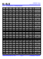
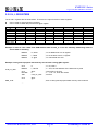
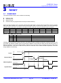
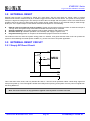
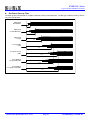
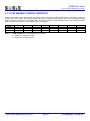
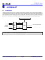
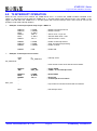
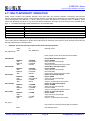
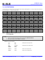
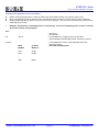
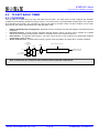
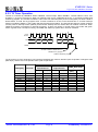
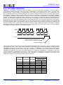
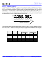
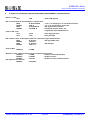
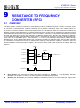
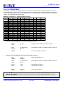
SN8P2318 Series C-type LCD, RFC 8-Bit Micro-Controller 5.7.3 P1W WAKEUP CONTROL REGISTER Under power down mode (sleep mode) and green mode, the I/O ports with wakeup function are able to wake the system up to normal mode. The wake-up trigger edge is level changing. When wake-up pin occurs rising edge or falling edge, the system is waked up by the trigger edge. The Port 0 and Port 1 have wakeup function. Port 0 wakeup function always enables, but the Port 1 is controlled by the P1W register. 0C0H P1W Read/Write After reset Bit[6:0] Bit 7 - Bit 6 P16W W 0 Bit 5 P15W W 0 Bit 4 P14W W 0 Bit 3 P13W W 0 Bit 2 P12W W 0 Bit 1 P11W W 0 Bit 0 P10W W 0 P10W~P16W: Port 1 wakeup function control bits. 0 = Disable P1n wakeup function. 1 = Enable P1n wakeup function. SONiX TECHNOLOGY CO., LTD Page 59 Preliminary Version 0.1 SN8P2318 Series C-type LCD, RFC 8-Bit Micro-Controller 6 INTERRUPT 6.1 OVERVIEW This MCU provides 5 interrupt sources, including 3 internal interrupt (T0/TC0/T1) and 2 external interrupt (INT0/INT1). The external interrupt can wake-up the chip while the system is switched from power down mode to high-speed normal mode, and interrupt request is latched until return to normal mode. Once interrupt service is executed, the GIE bit in STKP register will clear to “0” for stopping other interrupt request. On the contrast, when interrupt service exits, the GIE bit will set to “1” to accept the next interrupts’ request. The interrupt request signals are stored in INTRQ register. INTEN Interrupt Enable Register INT0 Trigger INT1 Trigger T0 Time Out TC0 Time Out T1 Time Out P00IRQ INTRQ 8-Bit & CMnM 2-Bit TC0IRQ Latchs T1IRQ P01IRQ T0IRQ Interrupt Interrupt Vector Address (0008H) Enable Gating Global Interrupt Request Signal Note: The GIE bit must enable during all interrupt operation. SONiX TECHNOLOGY CO., LTD Page 60 Preliminary Version 0.1 SN8P2318 Series C-type LCD, RFC 8-Bit Micro-Controller 6.2 INTEN INTERRUPT ENABLE REGISTER INTEN is the interrupt request control register including three internal interrupts, two external interrupts enable control bits. One of the register to be set “1” is to enable the interrupt request function. Once of the interrupt occur, the stack is incremented and program jump to ORG 8 to execute interrupt service routines. The program exits the interrupt service routine when the returning interrupt service routine instruction (RETI) is executed. 0C9H INTEN Read/Write After reset Bit 7 - Bit 6 T1IEN R/W 0 Bit 5 TC0IEN R/W 0 Bit 4 T0IEN R/W 0 Bit 0 P00IEN: External P0.0 interrupt (INT0) control bit. 0 = Disable INT0 interrupt function. 1 = Enable INT0 interrupt function. Bit 1 P01IEN: External P0.1 interrupt (INT1) control bit. 0 = Disable INT1 interrupt function. 1 = Enable INT1 interrupt function. Bit 4 T0IEN: T0 timer interrupt control bit. 0 = Disable T0 interrupt function. 1 = Enable T0 interrupt function. Bit 5 TC0IEN: TC0 timer interrupt control bit. 0 = Disable TC0 interrupt function. 1 = Enable TC0 interrupt function. Bit 6 T1IEN: T1 timer interrupt control bit. 0 = Disable T1 interrupt function. 1 = Enable T1 interrupt function. SONiX TECHNOLOGY CO., LTD Page 61 Bit 3 - Bit 2 - Bit 1 P01IEN R/W 0 Bit 0 P00IEN R/W 0 Preliminary Version 0.1 SN8P2318 Series C-type LCD, RFC 8-Bit Micro-Controller 6.3 INTRQ INTERRUPT REQUEST REGISTER INTRQ is the interrupt request flag register. The register includes all interrupt request indication flags. Each one of the interrupt requests occurs, the bit of the INTRQ register would be set “1”. The INTRQ value needs to be clear by programming after detecting the flag. In the interrupt vector of program, users know the any interrupt requests occurring by the register and do the routine corresponding of the interrupt request. 0C8H INTRQ Read/Write After reset Bit 7 - Bit 6 T1IRQ R/W 0 Bit 5 TC0IRQ R/W 0 Bit 4 T0IRQ R/W 0 Bit 0 P00IRQ: External P0.0 interrupt (INT0) request flag. 0 = None INT0 interrupt request. 1 = INT0 interrupt request. Bit 1 P01IRQ: External P0.1 interrupt (INT1) request flag. 0 = None INT1 interrupt request. 1 = INT1 interrupt request. Bit 4 T0IRQ: T0 timer interrupt request flag. 0 = None T0 interrupt request. 1 = T0 interrupt request. Bit 5 TC0IRQ: TC0 timer interrupt request flag. 0 = None TC0 interrupt request. 1 = TC0 interrupt request. Bit 6 T1IRQ: T1 timer interrupt request flag. 0 = None T1 interrupt request. 1 = T1 interrupt request. SONiX TECHNOLOGY CO., LTD Page 62 Bit 3 - Bit 2 - Bit 1 P01IRQ R/W 0 Bit 0 P00IRQ R/W 0 Preliminary Version 0.1 SN8P2318 Series C-type LCD, RFC 8-Bit Micro-Controller 6.4 GIE GLOBAL INTERRUPT OPERATION GIE is the global interrupt control bit. All interrupts start work after the GIE = 1 It is necessary for interrupt service request. One of the interrupt requests occurs, and the program counter (PC) points to the interrupt vector (ORG 8) and the stack add 1 level. 0DFH STKP Read/Write After reset Bit 7 Bit 7 GIE R/W 0 Bit 6 - Bit 5 - Bit 4 - Bit 3 - Bit 2 STKPB2 R/W 1 Bit 1 STKPB1 R/W 1 Bit 0 STKPB0 R/W 1 GIE: Global interrupt control bit. 0 = Disable global interrupt. 1 = Enable global interrupt. Example: Set global interrupt control bit (GIE). B0BSET FGIE ; Enable GIE Note: The GIE bit must enable during all interrupt operation. SONiX TECHNOLOGY CO., LTD Page 63 Preliminary Version 0.1 SN8P2318 Series C-type LCD, RFC 8-Bit Micro-Controller 6.5 PUSH, POP ROUTINE When any interrupt occurs, system will jump to ORG 8 and execute interrupt service routine. It is necessary to save ACC, PFLAG data. The chip includes “PUSH”, “POP” for in/out interrupt service routine. The two instructions save and load ACC, PFLAG data into buffers and avoid main routine error after interrupt service routine finishing. Note: ”PUSH”, “POP” instructions save and load ACC/PFLAG without (NT0, NPD). PUSH/POP buffer is an unique buffer and only one level. Example: Store ACC and PAFLG data by PUSH, POP instructions when interrupt service routine executed. ORG JMP 0 START ORG JMP 8 INT_SERVICE ORG 10H START: … INT_SERVICE: PUSH … … POP ; Save ACC and PFLAG to buffers. RETI … ENDP ; Exit interrupt service vector SONiX TECHNOLOGY CO., LTD ; Load ACC and PFLAG from buffers. Page 64 Preliminary Version 0.1 SN8P2318 Series C-type LCD, RFC 8-Bit Micro-Controller 6.6 EXTERNAL INTERRUPT OPERATION (INT0) INT0 is external interrupt trigger source and builds in edge trigger configuration function. When the external edge trigger occurs, the external interrupt request flag will be set to “1” no matter the external interrupt control bit enabled or disable. When external interrupt control bit is enabled and external interrupt edge trigger is occurring, the program counter will jump to the interrupt vector (ORG 8) and execute interrupt service routine. The external interrupt builds in wake-up latch function. That means when the system is triggered wake-up from power down mode, the wake-up source is external interrupt source (P0.0), and the trigger edge direction matches interrupt edge configuration, the trigger edge will be latched, and the system executes interrupt service routine fist after wake-up. 0BFH PEDGE Read/Write After reset Bit[4:3] Bit 7 - Bit 6 - Bit 5 - Bit 4 P00G1 R/W 0 Bit 3 P00G0 R/W 0 Bit 2 - Bit 1 - Bit 0 - P00G[1:0]: INT0 edge trigger select bits. 00 = reserved, 01 = rising edge, 10 = falling edge, 11 = rising/falling bi-direction. Example: Setup INT0 interrupt request and bi-direction edge trigger. MOV A, #98H B0MOV PEDGE, A ; Set INT0 interrupt trigger as bi-direction edge. B0BSET B0BCLR B0BSET FP00IEN FP00IRQ FGIE Example: INT0 interrupt service routine. ORG 8 JMP INT_SERVICE INT_SERVICE: … ; Enable INT0 interrupt service ; Clear INT0 interrupt request flag ; Enable GIE ; Interrupt vector ; Push routine to save ACC and PFLAG to buffers. B0BTS1 JMP FP00IRQ EXIT_INT ; Check P00IRQ ; P00IRQ = 0, exit interrupt vector B0BCLR … FP00IRQ ; Reset P00IRQ ; INT0 interrupt service routine EXIT_INT: … RETI SONiX TECHNOLOGY CO., LTD ; Pop routine to load ACC and PFLAG from buffers. ; Exit interrupt vector Page 65 Preliminary Version 0.1 SN8P2318 Series C-type LCD, RFC 8-Bit Micro-Controller 6.7 INT1 (P0.1) INTERRUPT OPERATION When the INT1 trigger occurs, the P01IRQ will be set to “1” no matter the P01IEN is enable or disable. If the P01IEN = 1 and the trigger event P01IRQ is also set to be “1”. As the result, the system will execute the interrupt vector (ORG 8). If the P01IEN = 0 and the trigger event P01IRQ is still set to be “1”. Moreover, the system won’t execute interrupt vector even when the P01IRQ is set to be “1”. Users need to be cautious with the operation under multi-interrupt situation. If the interrupt trigger direction is identical with wake-up trigger direction, the INT1 interrupt request flag (INT1IRQ) is latched while system wake-up from power down mode or green mode by P0.1 wake-up trigger. System inserts to interrupt vector (ORG 8) after wake-up immediately. Note: INT1 interrupt request can be latched by P0.1 wake-up trigger. Note: The interrupt trigger direction of P0.1 is falling edge. Example: INT1 interrupt request setup. B0BSET B0BCLR B0BSET FP01IEN FP01IRQ FGIE ; Enable INT1 interrupt service ; Clear INT1 interrupt request flag ; Enable GIE Example: INT1 interrupt service routine. ORG JMP 8 INT_SERVICE ; Interrupt vector INT_SERVICE: … ; Push routine to save ACC and PFLAG to buffers. B0BTS1 JMP FP01IRQ EXIT_INT ; Check P01IRQ ; P01IRQ = 0, exit interrupt vector B0BCLR … … FP01IRQ ; Reset P01IRQ ; INT1 interrupt service routine EXIT_INT: … ; Pop routine to load ACC and PFLAG from buffers. RETI ; Exit interrupt vector SONiX TECHNOLOGY CO., LTD Page 66 Preliminary Version 0.1 SN8P2318 Series C-type LCD, RFC 8-Bit Micro-Controller 6.8 T0 INTERRUPT OPERATION When the T0C counter occurs overflow, the T0IRQ will be set to “1” however the T0IEN is enable or disable. If the T0IEN = 1, the trigger event will make the T0IRQ to be “1” and the system enter interrupt vector. If the T0IEN = 0, the trigger event will make the T0IRQ to be “1” but the system will not enter interrupt vector. Users need to care for the operation under multi-interrupt situation. Example: T0 interrupt request setup. Fcpu = 4MHz / 4. B0BCLR B0BCLR MOV B0MOV MOV B0MOV FT0IEN FT0ENB A, #20H T0M, A A, #64H T0C, A ; Disable T0 interrupt service ; Disable T0 timer ; ; Set T0 clock = Fcpu / 64 ; Set T0C initial value = 64H ; Set T0 interval = 10 ms B0BSET B0BCLR B0BSET FT0IEN FT0IRQ FT0ENB ; Enable T0 interrupt service ; Clear T0 interrupt request flag ; Enable T0 timer B0BSET FGIE ; Enable GIE Example: T0 interrupt service routine. ORG JMP 8 INT_SERVICE ; Interrupt vector INT_SERVICE: … ; Push routine to save ACC and PFLAG to buffers. B0BTS1 JMP FT0IRQ EXIT_INT ; Check T0IRQ ; T0IRQ = 0, exit interrupt vector B0BCLR MOV B0MOV … … FT0IRQ A, #64H T0C, A ; Reset T0IRQ ; Reset T0C. ; T0 interrupt service routine EXIT_INT: … ; Pop routine to load ACC and PFLAG from buffers. RETI ; Exit interrupt vector SONiX TECHNOLOGY CO., LTD Page 67 Preliminary Version 0.1 SN8P2318 Series C-type LCD, RFC 8-Bit Micro-Controller 6.9 TC0 INTERRUPT OPERATION When the TC0C counter overflows, the TC0IRQ will be set to “1” no matter the TC0IEN is enable or disable. If the TC0IEN and the trigger event TC0IRQ is set to be “1”. As the result, the system will execute the interrupt vector. If the TC0IEN = 0, the trigger event TC0IRQ is still set to be “1”. Moreover, the system won’t execute interrupt vector even when the TC0IEN is set to be “1”. Users need to be cautious with the operation under multi-interrupt situation. Example: TC0 interrupt request setup. B0BCLR B0BCLR MOV B0MOV MOV B0MOV FTC0IEN FTC0ENB A, #20H TC0M, A A, #74H TC0C, A ; Disable TC0 interrupt service ; Disable TC0 timer ; ; Set TC0 clock = Fcpu / 64 ; Set TC0C initial value = 74H ; Set TC0 interval = 10 ms B0BSET B0BCLR B0BSET FTC0IEN FTC0IRQ FTC0ENB ; Enable TC0 interrupt service ; Clear TC0 interrupt request flag ; Enable TC0 timer B0BSET FGIE ; Enable GIE Example: TC0 interrupt service routine. ORG JMP 8 INT_SERVICE ; Interrupt vector INT_SERVICE: … ; Push routine to save ACC and PFLAG to buffers. B0BTS1 JMP FTC0IRQ EXIT_INT ; Check TC0IRQ ; TC0IRQ = 0, exit interrupt vector B0BCLR MOV B0MOV … … FTC0IRQ A, #74H TC0C, A ; Reset TC0IRQ ; Reset TC0C. ; TC0 interrupt service routine EXIT_INT: … ; Pop routine to load ACC and PFLAG from buffers. RETI ; Exit interrupt vector SONiX TECHNOLOGY CO., LTD Page 68 Preliminary Version 0.1 SN8P2318 Series C-type LCD, RFC 8-Bit Micro-Controller 6.10 T1 INTERRUPT OPERATION When the T1C (T1CH, T1CL) counter occurs overflow, the T1IRQ will be set to “1” however the T1IEN is enable or disable. If the T1IEN = 1, the trigger event will make the T1IRQ to be “1” and the system enter interrupt vector. If the T1IEN = 0, the trigger event will make the T1IRQ to be “1” but the system will not enter interrupt vector. Users need to care for the operation under multi-interrupt situation. Example: T1 interrupt request setup. B0BCLR B0BCLR MOV B0MOV CLR CLR FT1IEN FT1ENB A, #20H T1M, A T1CH T1CL ; Disable T1 interrupt service ; Disable T1 timer ; ; Set T1 clock = Fcpu / 32 and falling edge trigger. B0BSET B0BCLR B0BSET FT1IEN FT1IRQ FT1ENB ; Enable T1 interrupt service ; Clear T1 interrupt request flag ; Enable T1 timer B0BSET FGIE ; Enable GIE Example: T1 interrupt service routine. ORG JMP 8 INT_SERVICE ; Interrupt vector INT_SERVICE: PUSH ; Push routine to save ACC and PFLAG to buffers. B0BTS1 JMP FT1IRQ EXIT_INT ; Check T1IRQ ; T1IRQ = 0, exit interrupt vector B0BCLR B0MOV B0MOV B0MOV B0MOV CLR CLR … … FT1IRQ A, T1CH T1CHBUF, A A, T1CL T1CLBUF, A T1CH T1CL ; Reset T1IRQ ; Save pulse width. ; T1 interrupt service routine EXIT_INT: POP ; Pop routine to load ACC and PFLAG from buffers. RETI ; Exit interrupt vector SONiX TECHNOLOGY CO., LTD Page 69 Preliminary Version 0.1 SN8P2318 Series C-type LCD, RFC 8-Bit Micro-Controller 6.11 MULTI-INTERRUPT OPERATION Under certain condition, the software designer uses more than one interrupt requests. Processing multi-interrupt request requires setting the priority of the interrupt requests. The IRQ flags of interrupts are controlled by the interrupt event. Nevertheless, the IRQ flag “1” doesn’t mean the system will execute the interrupt vector. In addition, which means the IRQ flags can be set “1” by the events without enable the interrupt. Once the event occurs, the IRQ will be logic “1”. The IRQ and its trigger event relationship is as the below table. Interrupt Name P00IRQ P01IRQ T0IRQ TC0IRQ T1IRQ Trigger Event Description P0.0 trigger controlled by PEDGE P0.1 falling edge trigger T0C overflow TC0C overflow T1C (T1CH, T1CL) overflow For multi-interrupt conditions, two things need to be taking care of. One is to set the priority for these interrupt requests. Two is using IEN and IRQ flags to decide which interrupt to be executed. Users have to check interrupt control bit and interrupt request flag in interrupt routine. Example: Check the interrupt request under multi-interrupt operation ORG JMP 8 INT_SERVICE ; Interrupt vector INT_SERVICE: … ; Push routine to save ACC and PFLAG to buffers. INTP00CHK: B0BTS1 JMP B0BTS0 JMP FP00IEN INTT0CHK FP00IRQ INTP00 B0BTS1 JMP B0BTS0 JMP FP01IEN INTT0CHK FP01IRQ INTP01 B0BTS1 JMP B0BTS0 JMP FT0IEN INTTC0CHK FT0IRQ INTT0 B0BTS1 JMP B0BTS0 JMP FTC0IEN INTT1CHK FTC0IRQ INTTC0 B0BTS1 JMP B0BTS0 JMP … … FT1IEN … FT1IRQ INTT1 INTP01CHK: INTT0CHK: INTTC0CHK: INTT1CHK: ; Check INT0 interrupt request ; Check P00IEN ; Jump check to next interrupt ; Check P00IRQ ; Jump to INT0 interrupt service routine ; Check INT1 interrupt request ; Check P01IEN ; Jump check to next interrupt ; Check P01IRQ ; Jump to INT1 interrupt service routine ; Check T0 interrupt request ; Check T0IEN ; Jump check to next interrupt ; Check T0IRQ ; Jump to T0 interrupt service routine ; Check TC0 interrupt request ; Check TC0IEN ; Jump check to next interrupt ; Check TC0IRQ ; Jump to TC0 interrupt service routine ; Check T1 interrupt request ; Check T1IEN ; Jump check to next interrupt ; Check T1IRQ ; Jump to T1 interrupt service routine INT_EXIT: … ; Pop routine to load ACC and PFLAG from buffers. RETI ; Exit interrupt vector SONiX TECHNOLOGY CO., LTD Page 70 Preliminary Version 0.1 SN8P2318 Series C-type LCD, RFC 8-Bit Micro-Controller 7 I/O PORT 7.1 OVERVIEW The micro-controller builds in 29 pin I/O. Most of the I/O pins are mixed with analog pins and special function pins. The I/O shared pin list is as following. I/O Pin Shared Pin Shared Pin Control Condition Name Type Name Type P0.0 P0.1 P0.2 I/O I/O I/O P0.3 I P0.4 I/O P1.0 P1.1 P1.2 I/O I/O I/O I/O I/O I/O I/O I/O I/O I/O I/O INT0 INT1 T1IN RST VPP XOUT FCPUO RFC0 RFC1 RFC2 RFC3 RFC4 RFCOUT PWM0 SEG[28:31] SEG[24:27] SEG[20:23] SEG[16:19] DC DC DC DC HV AC DC AC AC AC AC AC DC DC DC DC DC DC P1.3 P1.4 P1.6 P5.4 P2[3:0] P2[7:4] P3[3:0] P3[7:4] P00IEN=1 P01IEN=1 T1CKS=1 Reset_Pin code option = Reset OTP Programming High_Clk code option = 4M, 12M High_Clk code option = RC RFCENB=1, RFCH[2:0]=000b RFCENB=1, RFCH[2:0]=001b RFCENB=1, RFCH[2:0]=010b RFCENB=1, RFCH[2:0]=011b RFCENB=1, RFCH[2:0]=100b RFCENB=1, RFCOUT=1 TC0ENB=1, PWMOUT=1 PSEG[2:0]=000b PSEG[2:0]=000b/001b PSEG[2:0]=000b/001b/010b PSEG[2:0]=000b/001b/010b/011b * DC: Digital Characteristic. AC: Analog Characteristic. HV: High Voltage Characteristic. SONiX TECHNOLOGY CO., LTD Page 71 Preliminary Version 0.1 SN8P2318 Series C-type LCD, RFC 8-Bit Micro-Controller 7.2 I/O PORT MODE The port direction is programmed by PnM register. When the bit of PnM register is “0”, the pin is input mode. When the bit of PnM register is “1”, the pin is output mode. 0B8H P0M Read/Write After reset Bit 7 - Bit 6 - Bit 5 - Bit 4 P04M R/W 0 Bit 3 - Bit 2 P02M R/W 0 Bit 1 P01M R/W 0 Bit 0 P00M R/W 0 0C1H P1M Read/Write After reset Bit 7 - Bit 6 P16M R/W 0 Bit 5 P15M R/W 0 Bit 4 P14M R/W 0 Bit 3 P13M R/W 0 Bit 2 P12M R/W 0 Bit 1 P11M R/W 0 Bit 0 P10M R/W 0 0C2H P2M Read/Write After reset Bit 7 P27M R/W 0 Bit 6 P26M R/W 0 Bit 5 P25M R/W 0 Bit 4 P24M R/W 0 Bit 3 P23M R/W 0 Bit 2 P22M R/W 0 Bit 1 P21M R/W 0 Bit 0 P20M R/W 0 0C3H P3M Read/Write After reset Bit 7 P37M R/W 0 Bit 6 P36M R/W 0 Bit 5 P35M R/W 0 Bit 4 P34M R/W 0 Bit 3 P33M R/W 0 Bit 2 P32M R/W 0 Bit 1 P31M R/W 0 Bit 0 P30M R/W 0 0C5H P5M Read/Write After reset Bit 7 - Bit 6 - Bit 5 - Bit 4 P54M R/W 0 Bit 3 - Bit 2 - Bit 1 - Bit 0 - Bit[7:0] PnM[7:0]: Pn mode control bits. (n = 0~5). 0 = Pn is input mode. 1 = Pn is output mode. Note: 1. Users can program them by bit control instructions (B0BSET, B0BCLR). 2. P0.3 input only pin, and the P0M.3 is undefined. Example: I/O mode selection. CLR CLR P0M P1M ; Set all ports to be input mode. MOV B0MOV B0MOV A, #0FFH P0M, A P1M,A ; Set all ports to be output mode. B0BCLR P1M.0 ; Set P1.0 to be input mode. B0BSET P1M.0 ; Set P1.0 to be output mode. SONiX TECHNOLOGY CO., LTD Page 72 Preliminary Version 0.1 SN8P2318 Series C-type LCD, RFC 8-Bit Micro-Controller Example: LCD shared pin control methods. ;Enable P2.0~P2.3 GPIO function. B0BCLR FPSEG2 B0BCLR FPSEG1 B0BSET FPSEG0 MOV B0MOV … B0BCLR A, #0X0F P2M, A ; Set P2.0~P2.3 to output mode. P2M.0 ; Set P2.0 to input mode. ;Enable P2.0~P2.7 GPIO function. B0BCLR FPSEG2 B0BSET FPSEG1 B0BCLR FPSEG0 MOV B0MOV … B0BCLR ; Set P2.0~P2.7 to output mode. P2M.0 ; Set P2.0 to input mode. ; Set PSEG[2:0]=011b A, #0XFF P2M, A A, #0X0F P3M, A ; Set P2.0~P2.7 to output mode. P2M.0 P3M.0 ; Set P2.0 to input mode. ; Set P3.0 to input mode. ;Enable P2.0~P2.7 and P3.0~P3.7 GPIO function. B0BSET FPSEG2 B0BCLR FPSEG1 B0BCLR FPSEG0 MOV B0MOV B0MOV … B0BCLR B0BCLR ; Set PSEG[2:0]=010b A, #0XFF P2M, A ;Enable P2.0~P2.7 and P3.0~P3.3 GPIO function. B0BCLR FPSEG2 B0BSET FPSEG1 B0BSET FPSEG0 MOV B0MOV MOV B0MOV … B0BCLR B0BCLR ; Set PSEG[2:0]=001b ; Set P3.0~P3.3 to output mode. ; Set PSEG[2:0]=100b A, #0XFF P2M, A P3M, A ; Set P2.0~P2.7 and P3.0~P3.7 to output mode. P2M.0 P3M.0 ; Set P2.0 to input mode. ; Set P3.0 to input mode. ;Disable P2.0~P2.7 and P3.0~P3.7 GPIO function. B0BCLR FPSEG2 B0BCLR FPSEG1 B0BCLR FPSEG0 SONiX TECHNOLOGY CO., LTD ; Set PSEG[2:0]=000b Page 73 Preliminary Version 0.1 SN8P2318 Series C-type LCD, RFC 8-Bit Micro-Controller 7.3 I/O PULL UP REGISTER The I/O pins build in internal pull-up resistors and only support I/O input mode. The port internal pull-up resistor is programmed by PnUR register. When the bit of PnUR register is “0”, the I/O pin’s pull-up is disabled. When the bit of PnUR register is “1”, the I/O pin’s pull-up is enabled. 0E0H P0UR Read/Write After reset Bit 7 - Bit 6 - Bit 5 - Bit 4 P04R W 0 Bit 3 - Bit 2 P02R W 0 Bit 1 P01R W 0 Bit 0 P00R W 0 0E1H P1UR Read/Write After reset Bit 7 - Bit 6 P16R W 0 Bit 5 P15R W 0 Bit 4 P14R W 0 Bit 3 P14R W 0 Bit 2 P12R W 0 Bit 1 P11R W 0 Bit 0 P10R W 0 0E2H P2UR Read/Write After reset Bit 7 P27R W 0 Bit 6 P26R W 0 Bit 5 P25R W 0 Bit 4 P24R W 0 Bit 3 P23R W 0 Bit 2 P22R W 0 Bit 1 P21R W 0 Bit 0 P20R W 0 0E3H P3UR Read/Write After reset Bit 7 P37R W 0 Bit 6 P36R W 0 Bit 5 P35R W 0 Bit 4 P34R W 0 Bit 3 P33R W 0 Bit 2 P32R W 0 Bit 1 P31R W 0 Bit 0 P30R W 0 0E5H P5UR Read/Write After reset Bit 7 - Bit 6 - Bit 5 - Bit 4 P54R W 0 Bit 3 - Bit 2 - Bit 1 - Bit 0 - Note: P0.3 is input only pin and without pull-up resister. The P0UR.3 is undefined. Example: I/O Pull up Register MOV B0MOV B0MOV A, #0FFH P0UR, A P1UR,A SONiX TECHNOLOGY CO., LTD ; Enable Port0, 1 Pull-up register, ; Page 74 Preliminary Version 0.1 SN8P2318 Series C-type LCD, RFC 8-Bit Micro-Controller 7.4 I/O PORT DATA REGISTER 0D0H P0 Read/Write After reset Bit 7 - Bit 6 - Bit 5 - Bit 4 P04 R/W 0 Bit 3 P03 R 0 Bit 2 P02 R/W 0 Bit 1 P01 R/W 0 Bit 0 P00 R/W 0 0D1H P1 Read/Write After reset Bit 7 - Bit 6 P16 R/W 0 Bit 5 P15 R/W 0 Bit 4 P14 R/W 0 Bit 3 P13 R/W 0 Bit 2 P12 R/W 0 Bit 1 P11 R/W 0 Bit 0 P10 R/W 0 0D2H P2 Read/Write After reset Bit 7 P27 R/W 0 Bit 6 P26 R/W 0 Bit 5 P25 R/W 0 Bit 4 P24 R/W 0 Bit 3 P23 R/W 0 Bit 2 P22 R/W 0 Bit 1 P21 R/W 0 Bit 0 P20 R/W 0 0D3H P3 Read/Write After reset Bit 7 P37 R/W 0 Bit 6 P36 R/W 0 Bit 5 P35 R/W 0 Bit 4 P34 R/W 0 Bit 3 P33 R/W 0 Bit 2 P32 R/W 0 Bit 1 P31 R/W 0 Bit 0 P30 R/W 0 0D5H P5 Read/Write After reset Bit 7 - Bit 6 - Bit 5 - Bit 4 P54 R/W 0 Bit 3 - Bit 2 - Bit 1 - Bit 0 - Note: The P03 keeps “1” when external reset enable by code option. Example: Read data from input port. B0MOV A, P0 B0MOV A, P1 Example: Write data to output port. MOV A, #0FFH B0MOV P0, A B0MOV P1, A Example: Write one bit data to output port. B0BSET P1.0 B0BCLR P1.0 SONiX TECHNOLOGY CO., LTD ; Read data from Port 0 ; Read data from Port 1 ; Write data FFH to all Port. ; Set P1.0 to be “1”. ; Set P1.0 to be “0”. Page 75 Preliminary Version 0.1 SN8P2318 Series C-type LCD, RFC 8-Bit Micro-Controller 8 TIMERS 8.1 WATCHDOG TIMER The watchdog timer (WDT) is a binary up counter designed for monitoring program execution. If the program goes into the unknown status by noise interference, WDT overflow signal raises and resets MCU. Watchdog clock controlled by code option and the clock source is internal low-speed oscillator. Watchdog overflow time = 8192 / Internal Low-Speed oscillator (sec). VDD 3V 5V Internal Low RC Freq. 16KHz 32KHz Watchdog Overflow Time 512ms 256ms The watchdog timer has three operating options controlled “WatchDog” code option. Disable: Disable watchdog timer function. Enable: Enable watchdog timer function. Watchdog timer actives in normal mode and slow mode. In power down mode and green mode, the watchdog timer stops. Always_On: Enable watchdog timer function. The watchdog timer actives and not stop in power down mode and green mode. In high noisy environment, the “Always_On” option of watchdog operations is the strongly recommendation to make the system reset under error situations and re-start again. Watchdog clear is controlled by WDTR register. Moving 0x5A data into WDTR is to reset watchdog timer. 0CCH WDTR Read/Write After reset Bit 7 WDTR7 W 0 Bit 6 WDTR6 W 0 Bit 5 WDTR5 W 0 Bit 4 WDTR4 W 0 Bit 3 WDTR3 W 0 Bit 2 WDTR2 W 0 Bit 1 WDTR1 W 0 Bit 0 WDTR0 W 0 Example: An operation of watchdog timer is as following. To clear the watchdog timer counter in the top of the main routine of the program. Main: MOV B0MOV … CALL CALL … JMP A, #5AH WDTR, A ; Clear the watchdog timer. SUB1 SUB2 MAIN Example: Clear watchdog timer by “@RST_WDT” macro of Sonix IDE. Main: @RST_WDT … CALL CALL … JMP ; Clear the watchdog timer. SUB1 SUB2 MAIN SONiX TECHNOLOGY CO., LTD Page 76 Preliminary Version 0.1 SN8P2318 Series C-type LCD, RFC 8-Bit Micro-Controller Watchdog timer application note is as following. Before clearing watchdog timer, check I/O status and check RAM contents can improve system error. Don’t clear watchdog timer in interrupt vector and interrupt service routine. That can improve main routine fail. Clearing watchdog timer program is only at one part of the program. This way is the best structure to enhance the watchdog timer function. Example: An operation of watchdog timer is as following. To clear the watchdog timer counter in the top of the main routine of the program. Main: Err: … … JMP $ ; Check I/O. ; Check RAM ; I/O or RAM error. Program jump here and don’t ; clear watchdog. Wait watchdog timer overflow to reset IC. Correct: MOV B0MOV … CALL CALL … … … JMP A, #5AH WDTR, A ; I/O and RAM are correct. Clear watchdog timer and ; execute program. ; Clear the watchdog timer. SUB1 SUB2 MAIN SONiX TECHNOLOGY CO., LTD Page 77 Preliminary Version 0.1 SN8P2318 Series C-type LCD, RFC 8-Bit Micro-Controller 8.2 T0 8-BIT BASIC TIMER 8.2.1 OVERVIEW The T0 timer is an 8-bit binary up timer with basic timer function. The basic timer function supports flag indicator (T0IRQ bit) and interrupt operation (interrupt vector). The interval time is programmable through T0M, T0C registers and supports RTC function. The T0 builds in green mode wake-up function. When T0 timer overflow occurs under green mode, the system will be waked-up to last operating mode. 8-bit programmable up counting timer: Generate time-out at specific time intervals based on the selected clock frequency. Interrupt function: T0 timer function supports interrupt function. When T0 timer occurs overflow, the T0IRQ actives and the system points program counter to interrupt vector to do interrupt sequence. RTC function: T0 supports RTC function. The RTC clock source is from external low speed 32K oscillator (LXIN/LXOUT) when T0TB=1. Green mode function: T0 timer keeps running in green mode and wakes up system when T0 timer overflows. T0 Rate (Fcpu/2~Fcpu/ 256) T0ENB Load T0C Value by Program. T0TB Fcpu Ext. 32K (LXIN, LXOUT) T0C 8-Bit Binary Up Counting Counter ÷ 64 T0IRQ Interrupt Flag (T0 timer overflow.) CPUM0,1 Note: In RTC mode, the T0 interval time is fixed at 0.5 sec and T0C is 256 counts. SONiX TECHNOLOGY CO., LTD Page 78 Preliminary Version 0.1 SN8P2318 Series C-type LCD, RFC 8-Bit Micro-Controller 8.2.2 T0 Timer Operation T0 timer is controlled by T0ENB bit. When T0ENB=0, T0 timer stops. When T0ENB=1, T0 timer starts to count. T0C increases “1” by timer clock source. When T0 overflow event occurs, T0IRQ flag is set as ”1” to indicate overflow and cleared by program. The overflow condition is T0C count from full scale (0xFF) to zero scale (0x00). T0 doesn’t build in double buffer, so load T0C by program when T0 timer overflows to fix the correct interval time. If T0 timer interrupt function is enabled (T0IEN=1), the system will execute interrupt procedure. The interrupt procedure is system program counter points to interrupt vector (ORG 8) and executes interrupt service routine after T0 overflow occurrence. Clear T0IRQ by program is necessary in interrupt procedure. T0 timer can works in normal mode, slow mode and green mode. In green mode, T0 keeps counting, set T0IRQ and wakes up system when T0 timer overflows. Clock Source T0C ... 0x00 or “n” by program 0x01 or n+1 0x02 or n+2 0x02 or n+2 ... ... 0xFE 0xFF 0x00 or “n” by program ... T0IRQ T0 timer overflows. T0IRQ set as “1”. Reload T0C by program. T0IRQ is cleared by program. T0 clock source is Fcpu (instruction cycle) through T0rate[2:0] pre-scaler to decide Fcpu/2~Fcpu/256. T0 length is 8-bit (256 steps), and the one count period is each cycle of input clock. T0rate[2:0] Fhosc=16MHz, Fcpu=Fhosc/4 T0 Clock T0 Interval Time Fhosc=4MHz, Fcpu=Fhosc/4 max. (ms) Unit (us) max. (ms) Unit (us) 000b 001b 010b 011b 100b 101b 110b 111b - Fcpu/256 Fcpu/128 Fcpu/64 Fcpu/32 Fcpu/16 Fcpu/8 Fcpu/4 Fcpu/2 32768Hz/64 SONiX TECHNOLOGY CO., LTD 16.384 8.192 4.096 2.048 1.024 0.512 0.256 0.128 - 64 32 16 8 4 2 1 0.5 - Page 79 65.536 32.768 16.384 8.192 4.096 2.048 1.024 0.512 - 256 128 64 32 16 8 4 2 - IHRC_RTC mode max. (sec) 0.5 Unit (ms) 1.953 Preliminary Version 0.1 SN8P2318 Series C-type LCD, RFC 8-Bit Micro-Controller 8.2.3 T0M MODE REGISTER T0M is T0 timer mode control register to configure T0 operating mode including T0 pre-scaler, clock source…These configurations must be setup completely before enabling T0 timer. 0D8H T0M Read/Write After reset Bit 7 T0ENB R/W 0 Bit 6 T0rate2 R/W 0 Bit 5 T0rate1 R/W 0 Bit 4 T0rate0 R/W 0 Bit 3 - Bit 2 - Bit 1 - Bit 0 T0TB R/W 0 Bit 0 T0TB: RTC clock source control bit. 0 = Disable RTC (T0 clock source from Fcpu). 1 = Enable RTC. Bit [6:4] T0RATE[2:0]: T0 timer clock source select bits. 000 = Fcpu/256, 001 = Fcpu/128, 010 = Fcpu/64, 011 = Fcpu/32, 100 = Fcpu/16, 101 = Fcpu/8, 110 = Fcpu/4,111 = Fcpu/2. Bit 7 T0ENB: T0 counter control bit. 0 = Disable T0 timer. 1 = Enable T0 timer. Note: T0RATE is not available in RTC mode. The T0 interval time is fixed at 0.5 sec. 8.2.4 T0C COUNTING REGISTER T0C is T0 8-bit counter. When T0C overflow occurs, the T0IRQ flag is set as “1” and cleared by program. The T0C decides T0 interval time through below equation to calculate a correct value. It is necessary to write the correct value to T0C register, and then enable T0 timer to make sure the first cycle correct. After one T0 overflow occurs, the T0C register is loaded a correct value by program. 0D9H T0C Read/Write After reset Bit 7 T0C7 R/W 0 Bit 6 T0C6 R/W 0 Bit 5 T0C5 R/W 0 Bit 4 T0C4 R/W 0 Bit 3 T0C3 R/W 0 Bit 2 T0C2 R/W 0 Bit 1 T0C1 R/W 0 Bit 0 T0C0 R/W 0 The equation of T0C initial value is as following. T0C initial value = 256 - (T0 interrupt interval time * T0 clock rate) Example: To calculation T0C to obtain 10ms T0 interval time. T0 clock source is Fcpu = 4MHz/4 = 1MHz. Select T0RATE=001 (Fcpu/128). T0 interval time = 10ms. T0 clock rate = 4MHz/4/128 T0C initial value = 256 - (T0 interval time * input clock) = 256 - (10ms * 4MHz / 4 / 128) = 256 - (10-2 * 4 * 106 / 4 / 128) = B2H Note: In RTC mode, T0C is 256 counts and generatesT0 0.5 sec interval time. Don’t change T0C value in RTC mode. SONiX TECHNOLOGY CO., LTD Page 80 Preliminary Version 0.1 SN8P2318 Series C-type LCD, RFC 8-Bit Micro-Controller 8.2.5 T0 TIMER OPERATION EXPLAME T0 TIMER CONFIGURATION: ; Reset T0 timer. MOV B0MOV A, #0x00 T0M, A ; Clear T0M register. ; Set T0 clock source and T0 rate. A, #0nnn0000b MOV B0MOV T0M, A ; Set T0C register for T0 Interval time. A, #value MOV B0MOV T0C, A ; Clear T0IRQ B0BCLR FT0IRQ ; Enable T0 timer and interrupt function. B0BSET FT0IEN B0BSET FT0ENB T0 works in RTC mode: ; Reset T0 timer. MOV B0MOV A, #0x00 T0M, A ; Set T0 RTC function. B0BSET FT0TB ; Enable T0 interrupt function. ; Enable T0 timer. ; Clear T0M register. ; Clear T0C. CLR T0C B0BCLR FT0IRQ ; Clear T0IRQ ; Enable T0 timer and interrupt function. B0BSET FT0IEN B0BSET FT0ENB SONiX TECHNOLOGY CO., LTD ; Enable T0 interrupt function. ; Enable T0 timer. Page 81 Preliminary Version 0.1 SN8P2318 Series C-type LCD, RFC 8-Bit Micro-Controller 8.3 TC0 8-BIT TIMER/COUNTER 8.3.1 OVERVIEW The TC0 timer is an 8-bit binary up timer with basic timer, event counter and PWM functions. The basic timer function supports flag indicator (TC0IRQ bit) and interrupt operation (interrupt vector). The interval time is programmable through TC0M, TC0C, TC0R registers. The event counter is changing TC0 clock source from system clock (Fcpu/Fhosc) to external clock like signal (e.g. continuous pulse, R/C type oscillating signal…). TC0 becomes a counter to count external clock number to implement measure application. TC0 also builds in duty/cycle programmable PWM. The PWM cycle and resolution are controlled by TC0 timer clock rate, TC0R and TC0D registers, so the PWM with good flexibility to implement IR carry signal, motor control and brightness adjuster…The main purposes of the TC0 timer are as following. 8-bit programmable up counting timer: Generate time-out at specific time intervals based on the selected clock frequency. Interrupt function: TC0 timer function supports interrupt function. When TC0 timer occurs overflow, the TC0IRQ actives and the system points program counter to interrupt vector to do interrupt sequence. Event Counter: The event counter function counts the external clock counts. Duty/cycle programmable PWM: The PWM is duty/cycle programmable controlled by TC0R and TC0D registers. Green mode function: All TC0 functions (timer, PWM, event counter, auto-reload) keep running in green mode and no wake-up function. TC0 Rate (Fcpu/1~Fcpu/128) TC0R Reload Data Buffer Up Counting Reload Value TC0CKS0 Load Fcpu TC0CKS1 TC0ENB Fhosc TC0 Time Out TC0C 8-Bit Binary Up Counting Counter PWM0OUT INT0 (Schmitter Trigger) PWM S CPUM0,1 P5.4 Pin Compare TC0D Data Buffer R P5.4 GPIO SONiX TECHNOLOGY CO., LTD Page 82 Preliminary Version 0.1 SN8P2318 Series C-type LCD, RFC 8-Bit Micro-Controller 8.3.2 TC0 TIMER OPERATION TC0 timer is controlled by TC0ENB bit. When TC0ENB=0, TC0 timer stops. When TC0ENB=1, TC0 timer starts to count. Before enabling TC0 timer, setup TC0 timer’s configurations to select timer function modes, e.g. basic timer, interrupt function…TC0C increases “1” by timer clock source. When TC0 overflow event occurs, TC0IRQ flag is set as ”1” to indicate overflow and cleared by program. The overflow condition is TC0C count from full scale (0xFF) to zero scale (0x00). In difference function modes, TC0C value relates to operation. If TC0C value changing effects operation, the transition of operations would make timer function error. So TC0 builds in double buffer to avoid these situations happen. The double buffer concept is to flash TC0C during TC0 counting, to set the new value to TC0R (reload buffer), and the new value will be loaded from TC0R to TC0C after TC0 overflow occurrence automatically. In the next cycle, the TC0 timer runs under new conditions, and no any transitions occur. The auto-reload function is no any control interface and always actives as TC0 enables. If TC0 timer interrupt function is enabled (TC0IEN=1), the system will execute interrupt procedure. The interrupt procedure is system program counter points to interrupt vector (ORG 8) and executes interrupt service routine after TC0 overflow occurrence. Clear TC0IRQ by program is necessary in interrupt procedure. TC0 timer can works in normal mode, slow mode and green mode. But in green mode, TC0 keep counting, set TC0IRQ and outputs PWM, but can’t wake-up system. Clock Source TC0C ... 0x00 or TC0R 0x01 0x02 0x03 ... ... 0xFE 0xFF TC0R ... TC0IRQ TC0 timer overflows. TC0IRQ set as “1”. Reload TC0C from TC0R automatically. TC0IRQ is cleared by program. TC0 provides different clock sources to implement different applications and configurations. TC0 clock source includes Fcpu (instruction cycle), Fhosc (high speed oscillator) and external input pin (P0.0) controlled by TC0CKS[1:0] bits. TC0CKS0 bit selects the clock source is from Fcpu or Fhosc. If TC0CKS0=0, TC0 clock source is Fcpu through TC0rate[2:0] pre-scaler to decide Fcpu/1~Fcpu/128. If TC0CKS0=1, TC0 clock source is Fhosc without any divider. TC0CKS1 bit controls the clock source is external input pin or controlled by TC0CKS0 bit. If TC0CKS1=0, TC0 clock source is selected by TC0CKS0 bit. If TC0CKS1=1, TC0 clock source is external input pin that means to enable event counter function. TC0rate[2:0] pre-scaler is unless when TC0CKS0=1 or TC0CKS1=1 conditions. TC0 length is 8-bit (256 steps), and the one count period is each cycle of input clock. TC0 Interval Time Fhosc=16MHz, TC0CKS0 TC0rate[2:0] TC0 Clock Fcpu=Fhosc/2 max. (ms) Unit (us) 0 000b Fcpu/128 4.096 16 0 001b Fcpu/64 2.048 8 0 010b Fcpu/32 1.024 4 0 011b Fcpu/16 0.576 2.25 0 100b Fcpu/8 0.256 1 0 101b Fcpu/4 0.128 0.5 0 110b Fcpu/2 0.064 0.25 0 111b Fcpu/1 0.032 0.125 1 useless Fhosc 0.016 0.0625 SONiX TECHNOLOGY CO., LTD Page 83 Preliminary Version 0.1 SN8P2318 Series C-type LCD, RFC 8-Bit Micro-Controller 8.3.3 TC0M MODE REGISTER TC0M is TC0 timer mode control register to configure TC0 operating mode including TC0 pre-scaler, clock source, PWM function…These configurations must be setup completely before enabling TC0 timer. 0DAH TC0M Read/Write After reset Bit 7 TC0ENB R/W 0 Bit 6 TC0rate2 R/W 0 Bit 5 TC0rate1 R/W 0 Bit 4 TC0rate0 R/W 0 Bit 3 TC0CKS1 R/W 0 Bit 2 TC0CKS0 R/W 0 Bit 1 - Bit 0 PWM0OUT R/W 0 Bit 0 PWM0OUT: PWM output control bit. 0 = Disable PWM output function, and P5.4 is GPIO mode. 1 = Enable PWM output function, and P5.4 outputs PWM signal. Bit 2 TC0CKS0: TC0 clock source select bit. 0 = Fcpu. 1 = Fhosc. TC0rate[2:0] bits are useless. Bit 3 TC0CKS1: TC0 clock source select bit. 0 = Internal clock (Fcpu and Fhosc controlled by TC0CKS0 bit). 1 = External input pin (P0.0/INT0) and enable event counter function. TC0rate[2:0] bits are useless. Bit [6:4] TC0RATE[2:0]: TC0 timer clock source select bits. 000 = Fcpu/128, 001 = Fcpu/64, 010 = Fcpu/32, 011 = Fcpu/16, 100 = Fcpu/8, 101 = Fcpu/4, 110 = Fcpu/2, 111 = Fcpu/1. Bit 7 TC0ENB: TC0 counter control bit. 0 = Disable TC0 timer. 1 = Enable TC0 timer. 8.3.4 TC0C COUNTING REGISTER TC0C is TC0 8-bit counter. When TC0C overflow occurs, the TC0IRQ flag is set as “1” and cleared by program. The TC0C decides TC0 interval time through below equation to calculate a correct value. It is necessary to write the correct value to TC0C register and TC0R register first time, and then enable TC0 timer to make sure the fist cycle correct. After one TC0 overflow occurs, the TC0C register is loaded a correct value from TC0R register automatically, not program. 0DBH TC0C Read/Write After reset Bit 7 TC0C7 R/W 0 Bit 6 TC0C6 R/W 0 Bit 5 TC0C5 R/W 0 Bit 4 TC0C4 R/W 0 Bit 3 TC0C3 R/W 0 Bit 2 TC0C2 R/W 0 Bit 1 TC0C1 R/W 0 Bit 0 TC0C0 R/W 0 The equation of TC0C initial value is as following. TC0C initial value = 256 - (TC0 interrupt interval time * TC0 clock rate) SONiX TECHNOLOGY CO., LTD Page 84 Preliminary Version 0.1 SN8P2318 Series C-type LCD, RFC 8-Bit Micro-Controller 8.3.5 TC0R AUTO-RELOAD REGISTER TC0 timer builds in auto-reload function, and TC0R register stores reload data. When TC0C overflow occurs, TC0C register is loaded data from TC0R register automatically. Under TC0 timer counting status, to modify TC0 interval time is to modify TC0R register, not TC0C register. New TC0C data of TC0 interval time will be updated after TC0 timer overflow occurrence, TC0R loads new value to TC0C register. But at the first time to setup TC0M, TC0C and TC0R must be set the same value before enabling TC0 timer. TC0 is double buffer design. If new TC0R value is set by st program, the new value is stored in 1 buffer. Until TC0 overflow occurs, the new value moves to real TC0R buffer. This way can avoid any transitional condition to effect the correctness of TC0 interval time and PWM output signal. 0CDH TC0R Read/Write After reset Bit 7 TC0R7 W 0 Bit 6 TC0R6 W 0 Bit 5 TC0R5 W 0 Bit 4 TC0R4 W 0 Bit 3 TC0R3 W 0 Bit 2 TC0R2 W 0 Bit 1 TC0R1 W 0 Bit 0 TC0R0 W 0 The equation of TC0R initial value is as following. TC0R initial value = 256 - (TC0 interrupt interval time * TC0 clock rate) Example: To calculation TC0C and TC0R value to obtain 10ms TC0 interval time. TC0 clock source is Fcpu = 16MHz/16 = 1MHz. Select TC0RATE=000 (Fcpu/128). TC0 interval time = 10ms. TC0 clock rate = 16MHz/16/128 TC0C/TC0R initial value = 256 - (TC0 interval time * input clock) = 256 - (10ms * 16MHz / 16 / 128) = 256 - (10-2 * 16 * 106 / 16 / 128) = B2H 8.3.6 TC0D PWM DUTY REGISTER TC0D register’s purpose is to decide PWM duty. In PWM mode, TC0R controls PWM’s cycle, and TC0D controls the duty of PWM. The operation is base on timer counter value. When TC0C = TC0D, the PWM high duty finished and exchange to low level. It is easy to configure TC0D to choose the right PWM’s duty for application. 0E8H TC0D Read/Write After Reset Bit 7 TC0D7 R/W 0 Bit 6 TC0D6 R/W 0 Bit 5 TC0D5 R/W 0 Bit 4 TC0D4 R/W 0 Bit 3 TC0D3 R/W 0 Bit 2 TC0D2 R/W 0 Bit 1 TC0D1 R/W 0 Bit 0 TC0D0 R/W 0 The equation of TC0D initial value is as following. TC0D initial value = TC0R + (PWM high pulse width period / TC0 clock rate) Example: To calculate TC0D value to obtain 1/3 duty PWM signal. The TC0 clock source is Fcpu = 16MHz/16= 1MHz. Select TC0RATE=000 (Fcpu/128). TC0R = B2H. TC0 interval time = 10ms. So the PWM cycle is 100Hz. In 1/3 duty condition, the high pulse width is about 3.33ms. TC0D initial value = B2H + (PWM high pulse width period / TC0 clock rate) = B2H + (3.33ms * 16MHz / 16 / 128) = B2H + 1AH = CCH SONiX TECHNOLOGY CO., LTD Page 85 Preliminary Version 0.1 SN8P2318 Series C-type LCD, RFC 8-Bit Micro-Controller 8.3.7 TC0 EVENT COUNTER TC0 event counter is set the TC0 clock source from external input pin (P0.0). When TC0CKS1=1, TC0 clock source is switch to external input pin (P0.0). TC0 event counter trigger direction is falling edge. When one falling edge occurs, TC0C will up one count. When TC0C counts from 0xFF to 0x00, TC0 triggers overflow event. The external event counter input pin’s wake-up function of GPIO mode is disabled when TC0 event counter function enabled to avoid event counter signal trigger system wake-up and not keep in power saving mode. The external event counter input pin’s external interrupt function is also disabled when TC0 event counter function enabled, and the P00IRQ bit keeps “0” status. The event counter usually is used to measure external continuous signal rate, e.g. continuous pulse, R/C type oscillating signal…These signal phase don’t synchronize with MCU’s main clock. Use TC0 event to measure it and calculate the signal rate in program for different applications. External Input Signel TC0C ... 0x00 or TC0R 0x01 0x02 0x03 ... ... 0xFE 0xFF TC0R ... TC0IRQ TC0 timer overflows. TC0IRQ set as “1”. Reload TC0C from TC0R automatically. TC0IRQ is cleared by program. 8.3.8 PULSE WIDTH MODULATION (PWM) The PWM is duty/cycle programmable design to offer various PWM signals. When TC0 timer enables and PWM0OUT bit sets as “1” (enable PWM output), the PWM output pin (P5.4) outputs PWM signal. One cycle of PWM signal is high pulse first, and then low pulse outputs. TC0R register controls the cycle of PWM, and TC0D decides the duty (high pulse width length) of PWM. TC0C initial value is TC0R reloaded when TC0 timer enables and TC0 timer overflows. When TC0C count is equal to TC0D, the PWM high pulse finishes and exchanges to low level. When TC0 overflows (TC0C counts from 0xFF to 0x00), one complete PWM cycle finishes. The PWM exchanges to high level for next cycle. The PWM is auto-reload design to load TC0C from TC0R automatically when TC0 overflows and the end of PWM’s cycle, to keeps PWM continuity. If modify the PWM cycle by program as PWM outputting, the new cycle occurs at next cycle when TC0C loaded from TC0R. Enable TC0 and PWM. TC0C is loaded from TC0R. PWM outputs high status. TC0C TC0R TC0R +1 TC0C = TC0D. PWM exchanges to low status. TC0R +2 ... TC0D -2 TC0D -1 TC0D ... 0xFD TC0C overflows from 0xFF to 0x00. TC0C is loaded from TC0R. PWM exchanges to high status. 0xFE 0xFF TC0R TC0R +1 TC0R +2 ... PWM Output One complete cycle of PWM. SONiX TECHNOLOGY CO., LTD Page 86 Next cycle. Preliminary Version 0.1 SN8P2318 Series C-type LCD, RFC 8-Bit Micro-Controller The resolution of PWM is decided by TC0R. TC0R range is from 0x00~0xFF. If TC0R = 0x00, PWM’s resolution is 1/256. If TC0R = 0x80, PWM’s resolution is 1/128. TC0D controls the high pulse width of PWM for PWM’s duty. When TC0C = TC0D, PWM output exchanges to low status. TC0D must be greater than TC0R, or the PWM signal keeps low status. When PWM outputs, TC0IRQ still actives as TC0 overflows, and TC0 interrupt function actives as TC0IEN = 1. But strongly recommend be careful to use PWM and TC0 timer together, and make sure both functions work well. The PWM output pin is shared with GPIO and switch to output PWM signal as PWM0OUT=1 automatically. If PWM0OUT bit is cleared to disable PWM, the output pin exchanges to last GPIO mode automatically. It easily to implement carry signal on/off operation, not to control TC0ENB bit. PWM Output PWM0OUT=0. PWM0OUT=1. The pin exchanges to output mode and outputs PWM signal automatically. PWM0OUT=0. The pin exchanges to last GPIO mode (output low). PWM0OUT=1. PWM0OUT=0. PWM0OUT=1. The pin exchanges to output mode and outputs PWM signal automatically. PWM0OUT=0. The pin exchanges to last GPIO mode (output high). PWM0OUT=1. PWM Output High impendence (floating) PWM Output PWM0OUT=0. PWM0OUT=1. The pin exchanges to output mode and outputs PWM signal automatically. PWM0OUT=0. The pin exchanges to last GPIO mode (input). PWM0OUT=1. 8.3.9 TC0 TIMER OPERATION EXPLAME TC0 TIMER CONFIGURATION: ; Reset TC0 timer. CLR TC0M ; Clear TC0M register. ; Set TC0 clock source and TC0 rate. A, #0nnn0n00b MOV B0MOV TC0M, A ; Set TC0C and TC0R register for TC0 Interval time. A, #value MOV B0MOV TC0C, A B0MOV TC0R, A ; TC0C must be equal to TC0R. ; Clear TC0IRQ B0BCLR FTC0IRQ ; Enable TC0 timer and interrupt function. B0BSET FTC0IEN B0BSET FTC0ENB SONiX TECHNOLOGY CO., LTD ; Enable TC0 interrupt function. ; Enable TC0 timer. Page 87 Preliminary Version 0.1 SN8P2318 Series C-type LCD, RFC 8-Bit Micro-Controller TC0 EVENT COUNTER CONFIGURATION: ; Reset TC0 timer. CLR TC0M ; Clear TC0M register. ; Enable TC0 event counter. B0BSET FTC0CKS1 ; Set TC0 clock source from external input pin (P0.0). ; Set TC0C and TC0R register for TC0 Interval time. A, #value MOV B0MOV TC0C, A B0MOV TC0R, A ; TC0C must be equal to TC0R. ; Clear TC0IRQ B0BCLR FTC0IRQ ; Enable TC0 timer and interrupt function. B0BSET FTC0IEN B0BSET FTC0ENB ; Enable TC0 interrupt function. ; Enable TC0 timer. TC0 PWM CONFIGURATION: ; Reset TC0 timer. CLR TC0M ; Clear TC0M register. ; Set TC0 clock source and TC0 rate. A, #0nnn0n00b MOV B0MOV TC0M, A ; Set TC0C and TC0R register for PWM cycle. A, #value1 MOV B0MOV TC0C, A B0MOV TC0R, A ; Set TC0D register for PWM duty. A, #value2 MOV B0MOV TC0D, A ; Enable PWM and TC0 timer. B0BSET B0BSET FTC0ENB FPWM0OUT SONiX TECHNOLOGY CO., LTD ; TC0C must be equal to TC0R. ; TC0D must be greater than TC0R. ; Enable TC0 timer. ; Enable PWM. Page 88 Preliminary Version 0.1 SN8P2318 Series C-type LCD, RFC 8-Bit Micro-Controller 8.4 T1 16-BIT TIMER WITH CAPTURE TIMER FUNCTION 8.4.1 OVERVIEW The T1 timer is a 16-bit binary up timer with basic timer and capture timer functions. The basic timer function supports flag indicator (T1IRQ bit) and interrupt operation (interrupt vector). The interval time is programmable through T1M, T1CH/T1CL 16-bit counter registers. The capture timer supports high pulse width measurement, low pulse width measurement, cycle measurement and continuous duration from P0.2/T1IN pin. T1 becomes a timer meter to count external signal time parameters to implement measure application. The main purposes of the T1 timer are as following. 16-bit programmable up counting timer: Generate time-out at specific time intervals based on the selected clock frequency. 16-bit capture timer: Measure the input signal pulse width and cycle depend on the T1 clock time base to decide the capture timer’s resolution. The capture timer builds in programmable trigger edge selection to decide the start-stop trigger event. 10-bit event counter: The 10-bit event counter to detect event source for accumulative capture timer function. The event counter is up counting design. When the counter is overflow, the T1 stops counting and the T1 counter buffers records the period of event counter duration. Interrupt function: T1 timer function and capture timer function support interrupt function. When T1 timer occurs overflow or capture timer stops counting, the T1IRQ actives and the system points program counter to interrupt vector to do interrupt sequence. Green mode function: All T1 functions (timer, event counter, capture timer, auto-reload) keeps running in green mode, but no wake-up function. T1CH Buffer T1 Rate (Fcpu/1~Fcpu/128) T1CL Buffer Read T1CL Register T1CKS Write T1CL Register T1ENB Fcpu T1IRQ Interrupt Flag (T1 timer overflow.) (Capture timer stop) T1CH,L 16-Bit Binary Up Counting Counter Fhosc CPUM0,1 P0.2/T1IN CPTStart RFC Output Signal CPTG[1:0] = 00, Disable. 01/10/11 = Enable. CPTVC CPTStart CPTCKS T1VC Counter Overflow CPTG[1:0] T1VC 10-bit Event Counter, Binary Up Counting Counter SONiX TECHNOLOGY CO., LTD Page 89 Preliminary Version 0.1 SN8P2318 Series C-type LCD, RFC 8-Bit Micro-Controller 8.4.2 T1 TIMER OPERATION T1 timer is controlled by T1ENB bit. When T1ENB=0, T1 timer stops. When T1ENB=1, T1 timer starts to count. Before enabling T1 timer, setup T1 timer’s configurations to select timer function modes, e.g. basic timer, interrupt function…T1 16-bit counter (T1CH, T1CL) increases “1” by timer clock source. When T1 overflow event occurs, T1IRQ flag is set as ”1” to indicate overflow and cleared by program. The overflow condition is T1CH, T1CL count from full scale (0xFFFF) to zero scale (0x0000). T1 doesn’t build in double buffer, so load T1CH, T1CL by program when T1 timer overflows to fix the correct interval time. If T1 timer interrupt function is enabled (T1IEN=1), the system will execute interrupt procedure. The interrupt procedure is system program counter points to interrupt vector (ORG 000FH) and executes interrupt service routine after T1 overflow occurrence. Clear T1IRQ by program is necessary in interrupt procedure. T1 timer can works in normal mode, slow mode and green mode. Clock Source T1CH, T1CL ... 0x0000 or “n” by program 0x0001 or n+1 0x0002 or n+2 0x0002 or n+2 ... ... 0xFFFE 0xFFFF 0x0000 or “n” by program ... T1IRQ T1 timer overflows. T1IRQ set as “1”. Reload T1CH, T1CL by program. T1IRQ is cleared by program. T1 provides different clock sources to implement different applications and configurations. T1 clock source includes Fcpu (instruction cycle) and Fhosc (high speed oscillator) controlled by T1CKS bit. T1CKS bit selects the clock source is from Fcpu or Fhosc. If T1CKS=0, T1 clock source is Fcpu through T1rate[2:0] pre-scalar to decide Fcpu/1~Fcpu/128. If T1CKS=1, T1 clock source is Fhosc. T1 length is 16-bit (65536 steps), and the one count period is each cycle of input clock. T1CKS T1rate[2:0] T1 Clock 0 0 0 0 0 0 0 0 1 000b 001b 010b 011b 100b 101b 110b 111b - Fcpu/128 Fcpu/64 Fcpu/32 Fcpu/16 Fcpu/8 Fcpu/4 Fcpu/2 Fcpu/1 Fhosc/1 SONiX TECHNOLOGY CO., LTD T1 Interval Time Fhosc=16MHz, Fhosc=4MHz, Fcpu=Fhosc/4 Fcpu=Fhosc/4 max. (ms) Unit (us) max. (ms) Unit (us) 2097.152 32 8388.608 128 1048.576 16 4194.304 64 524.288 8 2097.152 32 262.144 4 1048.576 16 131.072 2 524.288 8 65.536 1 262.144 4 32.768 0.5 131.072 2 16.384 0.25 65.536 1 4.096 0.0625 16.384 0.25 Page 90 Preliminary Version 0.1 SN8P2318 Series C-type LCD, RFC 8-Bit Micro-Controller 8.4.3 T1M MODE REGISTER T1M is T1 timer mode control register to configure T1 operating mode including T1 pre-scalar, clock source, capture parameters…These configurations must be setup completely before enabling T1 timer. 0A0H T1M Read/Write After reset Bit 7 T1ENB R/W 0 Bit 6 T1rate2 R/W 0 Bit 5 T1rate1 R/W 0 Bit 4 T1rate0 R/W 0 Bit 3 T1CKS R/W 0 Bit 2 Bit 1 Bit 0 Bit 7 T1ENB: T1 counter control bit. 0 = Disable T1 timer. 1 = Enable T1 timer. Bit [6:4] T1RATE[2:0]: T1 timer clock source select bits. If T1CKS0=1, the T1RATE[2:0] control is “Ignored”. 000 = Fcpu/128, 001 = Fcpu/64, 010 = Fcpu/32, 011 = Fcpu/16, 100 = Fcpu/8, 101 = Fcpu/4, 110 = Fcpu/2,111 = Fcpu/1. Bit 3 T1CKS: T1 clock source control bit. 0 = Fcpu divided by T1rate[2:0]. 1 = Fhosc. SONiX TECHNOLOGY CO., LTD Page 91 Preliminary Version 0.1 SN8P2318 Series C-type LCD, RFC 8-Bit Micro-Controller 8.4.4 T1CH, T1CL 16-bit COUNTING REGISTERS T1 counter is 16-bit counter combined with T1CH and T1CL registers. When T1 timer overflow occurs, the T1IRQ flag is set as “1” and cleared by program. The T1CH, T1CL decide T1 interval time through below equation to calculate a correct value. It is necessary to write the correct value to T1CH and T1CL registers, and then enable T1 timer to make sure the fist cycle correct. After one T1 overflow occurs, the T1CH and T1CL registers are loaded correct values by program. 0A1H T1CL Read/Write After reset 0A2H T1CH Read/Write After Reset Bit 7 T1CL7 R/W 0 Bit 7 T1CH7 R/W 0 Bit 6 T1CL6 R/W 0 Bit 6 T1CH6 R/W 0 Bit 5 T1CL5 R/W 0 Bit 4 T1CL4 R/W 0 Bit 3 T1CL3 R/W 0 Bit 2 T1CL2 R/W 0 Bit 1 T1CL1 R/W 0 Bit 0 T1CL0 R/W 0 Bit 5 T1CH5 R/W 0 Bit 4 T1CH4 R/W 0 Bit 3 T1CH3 R/W 0 Bit 2 T1CH2 R/W 0 Bit 1 T1CH1 R/W 0 Bit 0 T1CH0 R/W 0 The T1 timer counter length is 16-bit and points to T1CH and T1CL registers. The timer counter is double buffer design. The core bus is 8-bit, so access 16-bit data needs a latch flag to avoid the transient status affect the 16-bit data mistake occurrence. Under write mode, the write T1CH is the latch control flag. Under read mode, the read T1CL is the latch control flag. So, write T1 16-bit counter is to write T1CH first, and then write T1CL. The 16-bit data is written to 16-bit counter buffer after executing writing T1CL. Read T1 16-bit counter is to read T1CL first, and then read T1CH. The 16-bit data is dumped to T1CH, T1CL registers after executing reading T1CL. Read T1 counter buffer sequence is to read T1CL first, and then read T1CH. Write T1 counter buffer sequence is to write T1CH first, and then write T1CL. The equation of T1 16-bit counter (T1CH, T1CL) initial value is as following. T1CH, T1CL initial value = 65536 - (T1 interrupt interval time * T1 clock rate) Example: To calculation T1CH and T1CL values to obtain 500ms T1 interval time. T1 clock source is Fcpu = 16MHz/16 = 1MHz. Select T1RATE=000 (Fcpu/128). T1 interval time = 500ms. T1 clock rate = 16MHz/16/128 T1 16-bit counter initial value = 65536 - (T1 interval time * input clock) = 65536 - (500ms * 16MHz / 16 / 128) = 65536 - (500*10-3 * 16 * 106 / 16 / 128) = F0BDH (T1CH = F0H, T1CL = BDH) SONiX TECHNOLOGY CO., LTD Page 92 Preliminary Version 0.1 SN8P2318 Series C-type LCD, RFC 8-Bit Micro-Controller 8.4.5 T1 CPATURE TIMER OPERATION The 16-bit capture timer purpose is to measure input signal pulse width and cycle. The measure is through T1 timer by trigger selection. The capture timer is controlled by CPTG[1:0] bits. When CPTG[1:0] = 00, the capture timer is disabled. When CPTG[1:0] = 01/10/11, the capture timer is enabled, but the T1ENB must be enabled. The capture timer can measure input high pulse width, input low pulse width and the cycle of input signal controlled by CPTG[1:0]. CPTG[1:0] = 01, measure input high pulse width. CPTG[1:0] = 10, measure input low pulse width. CPTG[1:0] = 11, measure the cycle of input signal. The CPTG[1:0] only selects the capture timer function, not to execute the capture timer. CPTStart bit is to execute capture timer. When CPTStart is set as “1”, the capture timer waits the right trigger edge to active 16-bit counter. The trigger edge finds, and the 16-bit counter starts to count which clock source is T1. When the second right edge finds, the 16-counter stops, CPTStart is cleared and the T1IRQ actives. Before setting CPTStart bit, the T1 16-bit counter is cleared for capture timer initialization. High Pulse Width Measurement T1ENB = 1. CPTG[1:0] = 01. Input Signal T1 16-bit Counter Un-know Data 0x???? 0x0000 Initialization 1 2 n-1 n 0x0000 Initialization 1 T1 is counting. CPTStart = 1 Falling Edge T1 stops counting. CPTStart = 0 Rising Edge T1 starts to count. “n” is the high pulse width period. Read it by program through T1CH, T1CL registers. The high pulse width measurement is using rising edge to start T1 16-bit counter and falling edge to stop T1 16-bit counter. If set CPTStart bit at high pulse duration, the capture timer will measure next high pulse until the rising edge occurrence. Low Pulse Width Measurement T1ENB = 1. CPTG[1:0] = 10. Input Signal T1 16-bit Counter Un-know Data 0x???? 0x0000 Initialization 1 2 n-1 n 0x0000 Initialization 1 T1 is counting. CPTStart = 1 Rising Edge T1 stops counting. CPTStart = 0 Falling Edge T1 starts to count. “n” is the low pulse width period. Read it by program through T1CH, T1CL registers. The low pulse width measurement is using falling edge to start T1 16-bit counter and rising edge to stop T1 16-bit counter. If set CPTStart bit at low pulse duration, the capture timer will measure next low pulse until the falling edge occurrence. Input Cycle Measurement T1ENB = 1. CPTG[1:0] = 11. Input Signal T1 16-bit Counter Un-know Data 0x???? 0x0000 Initialization 1 2 n-1 n 0x0000 Initialization 1 T1 is counting. CPTStart = 1 Rising Edge T1 starts to count. Rising Edge T1 stops counting. CPTStart = 0 “n” is the cycle of input signal. Read it by program through T1CH, T1CL registers. The cycle measurement is using rising edge to start and stop T1 16-bit counter. If set CPTStart bit at high or low pulse duration, the capture timer will measure next cycle until the rising edge occurrence. SONiX TECHNOLOGY CO., LTD Page 93 Preliminary Version 0.1 SN8P2318 Series C-type LCD, RFC 8-Bit Micro-Controller 8.4.6 CAPTURE TIMER CONTROL REGISTERS A5H T1CKSM Read/Write After Reset Bit 7 CPTVC R/W 0 Bit 6 Bit 5 Bit 4 Bit 7 CPTVC: Event counter function control bit. 0 = Disable event counter function. 1 = Enable event counter function. Bit 3 CPTCKS: Capture timer clock source control bit. 0 = External input pin, P0.2/T1IN. 1 = RFC output terminal. Bit 2 CPTStart: Capture timer counter control bit. 0 = Process end. 1 = Start to count and processing. Bit [1:0] CPTG[1:0]: Capture timer function control bit. 00 = Disable capture timer function. 01 = High pulse width measurement. 10 = Low pulse width measurement. 11 = Cycle measurement. Bit 3 CPTCKS R/W 0 Bit 2 CPTStart R/W 0 Bit 1 CPTG1 R/W 0 Bit 0 CPTG0 R/W 0 8.4.7 10-bit Event Counter Function The 10-bit event timer purpose is to measure the period of a continuous input signal. The measure is through T1 timer by trigger selection. The event counter is controlled by CPTVC bit. When CPTVC = 0, the event counter is disabled. When CPTVC = 1, the event counter is enabled, but the T1ENB must be enabled. The event counter trigger edge is rising edge and must be set as CPTG[1:0] = 01 by program. The trigger edge finds, and the 10-bit event counter and T1 16-bit timer start to count. When T1 event counter overflows, T1 event counter and 16-bit timer stops counting and the T1IRQ actives. Before execute T1 event counter, the T1 16-bit counter must be cleared for initialization. Note: The event counter trigger edge is rising edge and must be set as CPTG[1:0] = 01 by program. Event Counter Operation Input Signal 10-bit Event Counter Set “m” by program m+1 m+2 CPTStart = 1 Un-know T1 16-bit CounterData 0x???? 1 0xFE 0x00 Event counter is overflow. T1 stops counting. CPTStart = 0 2 3 n-1 T1 is counting. n “n” is the period of (256-n) cycle of input signals. Read it by program through T1CH, T1CL registers. 0x0000 Initialization SONiX TECHNOLOGY CO., LTD 0xFF Page 94 Preliminary Version 0.1 SN8P2318 Series C-type LCD, RFC 8-Bit Micro-Controller Event Counter Trigger Format The capture timer input source has high pulse, low pulse and cycle signal. In event counter function, the trigger format is not like capture timer and fixed rising edge format. Use the start trigger signal of capture timer to be the event counter trigger source: Input Signal 10-bit Event Counter n n+1 n+2 n+3 n+4 n+5 8.4.8 T1VCH, T1VCL 10-bit EVENT COUNTER REGISTERS T1 event counter is 10-bit counter combined with T1VCH and T1VCL registers. When T1 event counter overflow occurs, the T1IRQ flag is set as “1” and cleared by program. The T1VCH, T1VCL decide T1 event counter number. 0A3H T1VCL Read/Write After reset 0A4H T1VCH Read/Write After Reset Bit 7 T1VCL7 R/W 0 Bit 7 - Bit 6 T1VCL6 R/W 0 Bit 6 - Bit 5 T1VCL5 R/W 0 Bit 4 T1VCL4 R/W 0 Bit 3 T1VCL3 R/W 0 Bit 2 T1VCL2 R/W 0 Bit 1 T1VCL1 R/W 0 Bit 0 T1VCL0 R/W 0 Bit 5 - Bit 4 - Bit 3 - Bit 2 - Bit 1 T1VCH1 R/W 0 Bit 0 T1VCH0 R/W 0 The T1 event counter length is 10-bit and points to T1VCH and T1VCL registers. The core bus is 8-bit, so access 10-bit data needs a latch flag to avoid the transient status affect the 10-bit data mistake occurrence. Under write mode, the write T1VCH is the latch control flag. Under read mode, the read T1VCL is the latch control flag. So, write T1 10-bit event counter is to write T1VCH first, and then write T1VCL. The 10-bit data is written to 10-bit counter buffer after executing writing T1VCL. Read T1 10-bit event counter is to read T1VCL first, and then read T1VCH. The 10-bit data is dumped to T1VCH, T1VCL registers after executing reading T1VCL. Read T1 event counter buffer sequence is to read T1VCL first, and then read T1VCH. Write T1 event counter buffer sequence is to write T1VCH first, and then write T1VCL. SONiX TECHNOLOGY CO., LTD Page 95 Preliminary Version 0.1 SN8P2318 Series C-type LCD, RFC 8-Bit Micro-Controller 8.4.9 T1 TIMER OPERATION EXPLAME T1 TIMER CONFIGURATION: ; Reset T1 timer. MOV B0MOV A, #0x00 T1M, A ; Clear T1M register. ; Set T1 clock rate. MOV B0MOV A, #0nnn0000b T1M, A ; T1rate[2:0] bits. ; Set T1CH, T1CL registers for T1 Interval time. A, #value1 MOV B0MOV T1CH, A A, #value2 MOV B0MOV T1CL, A ; Set high byte first. ; Set low byte. ; Clear T1IRQ B0BCLR FT1IRQ ; Enable T1 timer and interrupt function. B0BSET FT1IEN B0BSET FT1ENB ; Enable T1 interrupt function. ; Enable T1 timer. T1 CAPTURE TIMER FOR SINGLE CYCLE MEASUREMENT CONFIGURATION: ; Reset T1 timer. MOV B0MOV A, #0x00 T1M, A ; Clear T1M register. ; Set T1 clock rate, select input source, and select/enable T1 capture timer. A, #0nnnm000b MOV ; “nnn” is T1rate[2:0] for T1 clock rate selection. B0MOV T1M, A ; “m” is T1 clock source control bit. A, #000000mmb MOV ; “mm” is CPTG[1:0] for T1 capture timer function selection. B0MOV T1CKSM, A ; CPTG[1:0] = 01b, high pulse width measurement. ; CPTG[1:0] = 10b, low pulse width measurement. ; CPTG[1:0] = 11b, cycle measurement. ; Clear T1CH, T1CL. CLR CLR T1CH T1CL ; Clear high byte first. ; Clear low byte. ; Clear T1IRQ B0BCLR FT1IRQ ; Enable T1 timer, interrupt function and T1 capture timer function. B0BSET FT1IEN ; Enable T1 interrupt function. B0BSET FT1ENB ; Enable T1 timer. ; Set capture timer start bit. B0BSET FCPTStart SONiX TECHNOLOGY CO., LTD Page 96 Preliminary Version 0.1 SN8P2318 Series C-type LCD, RFC 8-Bit Micro-Controller T1 EVENT COUNTER FOR CONTINUOUS SIGNAL MEASUREMENT CONFIGURATION: ; Reset T1 timer. CLR T1M ; Clear T1M register. ; Set T1 clock rate and select/enable T1 capture timer. MOV A, #0nnnm000b ; “nnn” is T1rate[2:0] for T1 clock rate selection. B0MOV T1M, A ; “m” is T1 clock source control bit. MOV A, #00000001b ; Set capture timer function. B0MOV T1CKSM, A ; CPTG[1:0] must be set as “01”. ; “High pulse width measurement” ; Clear T1CH, T1CL. CLR T1CH ; Clear high byte first. CLR T1CL ; Clear low byte. ; Set T1VCH, T1VCL 10-bit capture timer for continuous signal measurement. MOV A, #value1 ; Set high nibble first. B0MOV T1VCH, A MOV A, #value2 ; Set low byte. B0MOV T1VCL, A ; Clear T1IRQ B0BCLR FT1IRQ ; Enable T1 timer, interrupt function and T1 capture timer function. B0BSET FT1IEN ; Enable T1 interrupt function. B0BSET FT1ENB ; Enable T1 timer. B0BSET FCPTVC ; Enable T1 event counter function. ; Set capture timer start bit. B0BSET FCPTStart SONiX TECHNOLOGY CO., LTD Page 97 Preliminary Version 0.1 SN8P2318 Series C-type LCD, RFC 8-Bit Micro-Controller 9 RESISTANCE TO FREQURNCY CONVERTER (RFC) 9.1 OVERVIEW The MCU builds in resistance to frequency converter (RFC) CR type oscillation converter. The RFC conversion circuit is connecting a resistive sensor, reference resistance and a capacitor. Resistance value of the resistive sensor or reference resistance connected to the RFC channel input is converted into frequency by CR oscillator and the number of clocks is counted in the built-in measurement timer/counter (T1). Reading the value of T1 measurement obtains the digitally converting value detected by the resistance. Various sensor circuits such as temperature measurement using a thermistor can easily realize using the RFC. The RFC includes 5 channels. One channel is used reference channel, and the other channels are sensor input channels. For different resistive sensor, the RFC clock frequency is different. T1 provides pulse width measurement and input frequency measurement functions to measure high/low speed RFC clock. RFC pin is shared with port 1. When RFCENB = 1, P1.0~P1.4 are selected to RFC0~RFC4 channel through RFCH[2:0] bits. P1.6 is shared with RFCOUT pin controlled by RFCOUT bit of RFCM register. Each of RFC channels is connected to T1capture timer function to measure RFC frequency and does RFC oscillation. These RFC pins are shared with GPIO controlled by RFCM register. RFC function actives under green mode, but not support wake-up function. RFCENB P1.0/RFC0 RFCENB P1.1/RFC1 RFC Oscillation Generator P1.2/RFC2 T1 Capture Timer P1.3/RFC3 P1.4/RFC4 RFCH[2:0] RFCENB P1.6/RFCOUT RFCOUT RFC Channel: RFC channels are shared with GPIO controlled by RFCENB = 1 and RFCH[2:0] selected. RFCENB=1 is necessary, or the RFC channel selected by RFCH[2:0] is GPIO mode. RFCOUT pin: RFC output pin is shared with GPIO controlled by RFCOUT bit. RFC output pin outputs RFC oscillating signal through RFC oscillator generator processing. The signal also inputs to T1 capture timer. SONiX TECHNOLOGY CO., LTD Page 98 Preliminary Version 0.1 SN8P2318 Series C-type LCD, RFC 8-Bit Micro-Controller 9.2 RFC APPLICATION CIRCUIT RFC application is configured a resistive device and a capacitor. Normally, the resistor is a sensor type device and the capacitor is a static device. The connection diagram is as following. The resistor connects from Vdd to RFC channel, and the capacitor connects from Vss to RFC channel. When RFC function actives, the internal RFC oscillation generator makes the RFC channel oscillating. The frequency depends on R and C value. RFCOUT R1 R2 R3 R4 R5 RFC0 RFC1 RFC2 RFC3 RFC4 C1 C2 C3 C4 MCU C5 VCC GND These RC circuits are switched by RFCH[2:0] bits of RFCM register. If one RFC input is selected, the other pins switch to GPIO mode. Recommend set RFC0~RFC4 (P1.0~P1.4) as input floating. RFC digitally converting clock is output from RFCOUT pin (P1.6) controlled by RFCOUT bit of RFC register. 9.3 RFC OPERATION VDD To T1 RFC Measurement Counter (1) (2) R RFC Oscillation Generator (2) RFC Channel C (1) VSS RFC operation is base on charge and discharge capacitor to obtain the converting clock. The RFCENB=1 turns on RFC function. RFC channel charges the external RC circuit until the voltage level higher than ViH of RFC cahnnel. Then RFC channel exchanges to discharge operation until voltage level under ViL. The charge/discharge operation obtains the RFC oscillation. Loop (1) of above figure is charge mode. The capacitor is charged by RFC channel, and the voltage level increases. RFC channel detects the voltage level to Schmitt trigger high-level voltage, and then RFC channel switches to discharge mode. Loop (2) is discharge mode. RFC channel discharges and the voltage level starts to fall down. RFC channel detects the voltage level to Schmitt trigger low-level voltage, and then RFC channel switches to charge mode. The result of charge and discharge switching is converted by RC oscillation control circuit and generate digitally clock. High Level of Schmitt trigger RFC Input Signal Low Level of Schmitt trigger Discharge Charge VDD RFC Clock & RFCOUT (RFC Output) VSS The reference capacitor value is steady. The RFC clock frequency value depends on resistance value and determines charge and discharge rate. Using the RFC clocks of reference resistance and resistive sensor can measure the sensor resistance by the frequency of RFC converting result. The RFC clock can be T1 clock source to measure RFC converting value by frequency measurement and pulse width measurement. The RFC clock also can output to RFCOUT pin (P1.6) when RFCOUT =1. SONiX TECHNOLOGY CO., LTD Page 99 Preliminary Version 0.1 SN8P2318 Series C-type LCD, RFC 8-Bit Micro-Controller 9.4 RFCM REGISTER 0A6H RFCM Read/Write After reset Bit 7 RFCENB R/W 0 Bit 6 - Bit 5 0 W 0 Bit 4 1 W 0 Bit 3 RFCOUT R/W 0 Bit 2 RFCH2 R/W 0 Bit 1 RFCH1 R/W 0 Bit 7 RFCENB: RFC function control bit. 0 = Disable RFC function. 1 = Enable RFC function. Bit 5 Bit 4 RFCM.5 must be set as “0” by program. RFCM.4 must be set as “1” by program. Bit 3 RFCOUT: RFC output control bit. 0 = Disable RFC output, P1.6 is general purpose I/O. 1 = Enable RFC output, P1.6 is RFCOUT pin. Bit[2:1] RFCH[2:1]: RFC input channels select bit. 000 = Select RFC0 channel. Disable P1.0 GPIO function. P1.1, P1.2, P1.3, P1.4 are GPIO mode. 001 = Select RFC1 channel. Disable P1.1 GPIO function. P1.0, P1.2, P1.3, P1.4 are GPIO mode. 010 = Select RFC2 channel. Disable P1.2 GPIO function. P1.0, P1.1, P1.3, P1.4 are GPIO mode. 011 = Select RFC3 channel. Disable P1.3 GPIO function. P1.0, P1.1, P1.2, P1.4 are GPIO mode. 100 = Select RFC4 channel. Disable P1.4 GPIO function. P1.0, P1.1, P1.2, P1.3 are GPIO mode. 101~111 = Reserved. P1.0, P1.1, P1.2, P1.3, P1.4 are GPIO mode. Bit 0 RFCH0 R/W 0 Note: 1. Before RFC enable, P1.0~P1.4 must be set as input mode without pull-up resistor first by program. 2. RFCM.4 must be set as “1” by program through MOV/B0MOV instruction because the bit is write only type. 3. RFCM.5 must be set as “0” by program through MOV/B0MOV instruction because the bit is write only type. 4. We strongly recommend controlling RFCM register through MOV/B0MOV instructions. SONiX TECHNOLOGY CO., LTD Page 100 Preliminary Version 0.1 SN8P2318 Series C-type LCD, RFC 8-Bit Micro-Controller 9.5 RFC OPERATION EXPLAME Example: Measure RFC signal through T1 event counter function. ; Set T1 timer mode. CLR MOV B0MOV B0MOV T1M A, #0 T1CH, A T1CL, A ; T1 clock is Fcpu and rate is Fcpu/256. ; Clear T1 counter buffers. ; Set T1 event counter mode. MOV B0MOV MOV B0MOV MOV B0MOV A, #10001000B T1CKSM, A A, #0 T1VCH, A A, #0xFF T1VCL, A ; Configure and enable T1 capture timer. B0BCLR FT1IRQ ; Clear T1 interrupt request flag. CLR MOV AND MOV B0MOV P1UR A, #11100000B P1M, A A, #10010000B RFCM, A ; Disable P1 pull-up resistor. B0BSET B0BSET FT1ENB FCPTStart ; Enable T1 timer. ; Start to measure RFC frequency. FT1IRQ Chk_T1IRQ A, T1CL ; Check T1IRQ=1. ; Set T1 event counter buffers. ; Set RFC. ; Check T1IRQ=1. Chk_T1IRQ: B0BTS1 JMP B0MOV … B0MOV … ; Set P1.0~P1.4 to input mode. ; Enable RFC and select RFC channel 0. ; The end of RFC measurement. A, T1CH SONiX TECHNOLOGY CO., LTD Page 101 Preliminary Version 0.1 SN8P2318 Series C-type LCD, RFC 8-Bit Micro-Controller 10 4x32 LCD DRIVER 10.1 OVERVIEW The LCD driver density is 4x32 (4 commons and 32 segments, 128 dots) and builds in C-type and R-type structure. The LCD supports 1/4 duty and 1/2, 1/3 bias LCD panel. The LCD frame rate is 64Hz and clock source is external 32768Hz oscillator crystal or RC type. The C-type only supports 1/3 bias LCD structure. R-type is using external bias circuit to adjust LCD power and bias voltage. There are 16-pin GPIO shared with SEGs controlled by register. For difference density LCD panel, users can decides more GPIO pins for application. 10.2 LCD REGISTERS 0CBH LCDM Read/Write After reset Bit [7:6] Bit 7 CPCK1 R/W 0 Bit 6 CPCK0 R/W 0 Bit 5 VLCDCP R/W 0 Bit 4 PSEG2 R/W 0 Bit 3 PSEG1 R/W 0 Bit 2 PSEG0 R/W 0 Bit 1 BIAS R/W 0 Bit 0 LCDENB R/W 0 CPCK[1:0]: VLCD charge-pump clock selection. CPCK[1:0] Charge-pump Clock 00 32KHz 01 16KHz 10 4KHz 11 1KHz Note: In general speaking, 1KHz charge-pump clock is enough for most application. Lower charge-pump clock frequency can save more power consumption. Higher charge-pump clock frequency can provide stronger VLCD driving capability. Bit 5 VLCDCP: VLCD charge-pump control bit. 0 = Disable. LCD is R-type. 1 = Enable. LCD is C-type. Bit [4:2] PSEG2: LCD shared pin control bit. 000 = Disable all LCD shared pins’ GPIO function. The SEG pin number is 32. 001 = Enable P2.0~P2.3 (SEG28~SEG31) GPIO function. The SEG pin number is 28. 010 = Enable P2.0~P2.7 (SEG24~SEG31) GPIO function. The SEG pin number is 24. 011 = Enable P2.0~P2.7 and P3.0~P3.3 (SEG20~31) GPIO function. The SEG pin number is 20. 100 = Enable P2.0~P2.7 and P3.0~P3.7 (SEG16~31) GPIO function. The SEG pin number is 16. 101~111 = Reserved. Bit 1 BIAS: LCD bias control bit. 0 = 1/3 bias (C type and R type). 1 = 1/2 bias (R type only). Bit 0 LCDENB: LCD control bit. 0 = Disable. 1 = Enable. SONiX TECHNOLOGY CO., LTD Page 102 Preliminary Version 0.1 SN8P2318 Series C-type LCD, RFC 8-Bit Micro-Controller 10.3 C-TYPE LCD MODE In C-type mode only support 1/3 bias LCD panel. The LCD power (VLCD) is supplied by internal charge-pump. The power consumption of C-type mode is less than R-type, because no external DC bias circuit expenses power current. The charge-pump voltage level is following VLCD voltage. V1 is the charge pump source which level is 1/3*VLCD. V2 is 2 times of V1 by charge pump which level is 2/3*VLCD. In C-type LCD mode, the VLCDCP bit of VLCD register must be “1”. VLCD Power Source LXIN 10pF 32768Hz 10pF VLCD 0.1uF V2 0.1uF V1 0.1uF LXOUT MCU VSS COM0~COM3 Charge-Pump Output Voltage LCD PANEL SEG0~SEG31 C+ C- VSS 0.1uF Basic C type LCD Application Circuit LCD C-type mode only supports 1/3 bias. In C-type mode, connect a 0.1uF capacitor between C+ and C- pins. The 0.1uF capacitors of VLCD/V1/V2 pins are necessary for power stable. V1 voltage is charge-pump source voltage and 1/3*VLCD. V2 voltage is 2*V1 = 2/3*VLCD. Note: The VLCD voltage source is from external power source depended on LCD panel power level, and VLCD voltage level can’t be larger than MCU’s Vdd. Example : The configuration of C-type LCD mode. ; Set C-type LCD. MOV B0MOV A, #nn0mmm00B LCDM ; “nn” selects charge pump clock rate. ; “mmm” controls P2/P3 LCD shared pins. ; BIAS = 0 for 1/3 bias structure. ; Enable charge pump. B0BSET FVLCDCP ; Enable LCD charge-pump and LCD is switched to ; C-type mode. ; Enable LCD driver. B0BSET FLCDENB ; Enable LCD driver.. ; LCD picture process. … … SONiX TECHNOLOGY CO., LTD Page 103 Preliminary Version 0.1 SN8P2318 Series C-type LCD, RFC 8-Bit Micro-Controller 10.4 R-TYPE LCD MODE In R-type mode, LCD power (VLCD) is connected with internal VDD. V1, V2 bias voltage is controlled by external resistor. The bias resistors determine LCD V1, V2 bias voltage and LCD driver current. Too much current makes LCD panel to bring remnant images. In normal condition, the suggestion of the external bias resistor’s value is 100Kohm. In R-type LCD mode, the VLCDCP bit of VLCD register must be “0”. LCD Bias 1/3 Bias (Bias=0) 1/2 Bias (Bias=1) VLCD VDD VDD V2 2/3*VDD 1/2*VDD V1 1/3*VDD 1/2*VDD VLCD Power Source VLCD MCU VLCD Power Source VLCD 0.1uF V2 100Kohm 0.1uF V1 100Kohm 0.1uF 100Kohm V2 MCU 100Kohm VSS C+ 0.1uF V1 0.1uF 100Kohm VSS VSS C- C+ 1/3 bias, 1/4 duty, R-type LCD Circuit. VSS C- 1/2 bias, 1/4 duty, R-type LCD Circuit. In R-type mode, C+/C- don’t connect any devices. 1/2 bias, V2 connects to V1. The 0.1uF capacitors of VLCD/V1/V2 pins are necessary for power stable. Note: Note: The VLCD voltage source is from external power source depended on LCD panel power level, and VLCD voltage level can’t be larger than MCU’s Vdd. Example : The configuration of R-type LCD mode. ; Set C-type LCD. MOV B0MOV A, #000mmmn0B LCDM ; “n” selects bias. ; “mmm” controls P2/P3 LCD shared pins. ; Enable LCD driver. B0BSET FLCDENB ; Enable LCD driver.. ; LCD picture process. … … SONiX TECHNOLOGY CO., LTD Page 104 Preliminary Version 0.1 SN8P2318 Series C-type LCD, RFC 8-Bit Micro-Controller 10.5 LCD RAM MAP LCD dots are controlled by LCD RAM in Bank15. Program the LCD RAM data is using index pointer in bank 0 or directly addressing in bank 15. The LCD RAM placement is by LCD segments. One segment address includes four common bits data. COM0~COM3 is in low-nibble of one LCD RAM (bit0~bit3). The high-nibble of one LCD RAM is useless. The LCD RAM map is as following. RAM bank 15 address vs. Common/Segment location. RAM Address 00h 01h 02h 03h . . . 0Ch 0Dh 0Eh 0Fh 10h . . . 1Bh 1Ch 1Dh 1Eh 1Fh Bit LCD SEG0 SEG1 SEG2 SEG3 . . . SEG12 SEG13 SEG14 SEG15 SEG16 . . . SEG27 SEG28 SEG29 SEG30 SEG31 0 COM0 00h.0 01h.0 02h.0 03h.0 . . . 0Ch.0 0Dh.0 0Eh.0 0Fh.0 10h.0 . . . 1Bh.0 1Ch.0 1Dh.0 1Eh.0 1Fh.0 1 COM1 00h.1 01h.1 02h.1 03h.1 . . . 0Ch.1 0Dh.1 0Eh.1 0Fh.1 10h.1 . . . 1Bh.1 1Ch.1 1Dh.1 1Eh.1 1Fh.1 2 COM2 00h.2 01h.2 02h.2 03h.2 . . . 0Ch.2 0Dh.2 0Eh.2 0Fh.2 10h.2 . . . 1Bh.2 1Ch.2 1Dh.2 1Eh.2 1Fh.2 3 COM3 00h.3 01h.3 02h.3 03h.3 . . . 0Ch.3 0Dh.3 0Eh.3 0Fh.3 10h.3 . . . 1Bh.3 1Ch.3 1Dh.3 1Eh.3 1Fh.3 4 - 5 - 6 - 7 - Example : Set LCD RAM data by index pointer (@YZ) in bank 0. B0MOV CLR Y, #0FH Z ; Set @YZ point to LCD RAM address 0x1500. MOV B0MOV A, #00001010B @YZ, A ; Set COM0=0, COM1=1, OCM2=0,COM3=1 of SEG 0. INCMS … … Z ; Point to next segment address. Example : Set LCD RAM data by directly addressing in bank 15. MOV B0MOV A, #01 RBANK, A ; Switch to RAM bank 15. MOV MOV A, #00001010B 00H, A ; Set COM0=0, COM1=1, OCM2=0,COM3=1 of SEG 0. BCLR BSET … 01H.0 01H.1 ; Clear COM0=0 of SEG 1. ; Clear COM1=1 of SEG 1. MOV B0MOV A, #0 RBANK, A ; Switch to RAM bank 0. Note: Access RAM data of bank 0 (system registers and user define RAM 0x0000~0x007F) is using “B0xxx” instructions. SONiX TECHNOLOGY CO., LTD Page 105 Preliminary Version 0.1 SN8P2318 Series C-type LCD, RFC 8-Bit Micro-Controller 10.6 LCD WAVEFORM 1/2 bias, 1/4 duty 1/3 bias, 1/4 duty LCD Clock LCD Clock 1 Frame 1 Frame 1 Frame 1 Frame VLCD VLCD COM0 1/2*VLCD 2/3*VLCD COM0 1/3*VLCD VSS VSS VLCD COM1 VLCD 1/2*VLCD 2/3*VLCD COM1 VSS 1/3*VLCD VSS VLCD COM2 1/2*VLCD VLCD VSS 2/3*VLCD COM2 1/3*VLCD VLCD COM3 VSS 1/2*VLCD VLCD VSS 2/3*VLCD COM3 SEG0 (1010b) VLCD 1/3*VLCD 1/2*VLCD VSS VSS ON OFF ON OFF ON OFF ON VLCD OFF 2/3*VLCD SEG0 (1010b) 1/3*VLCD VLCD SEG0 (0101b) VSS 1/2*VLCD ON OFF ON OFF ON OFF ON OFF VSS OFF ON OFF ON OFF ON OFF VLCD ON 2/3*VLCD SEG0 (0101b) 1/3*VLCD VSS OFF SONiX TECHNOLOGY CO., LTD Page 106 ON OFF ON OFF ON OFF ON Preliminary Version 0.1 SN8P2318 Series C-type LCD, RFC 8-Bit Micro-Controller 11 INSTRUCTION TABLE Field M O V E A R I T H M E T I C L O G I C Mnemonic MOV A,M MOV M,A B0MOV A,M B0MOV M,A MOV A,I B0MOV M,I XCH A,M B0XCH A,M MOVC Description AM MA A M (bank 0) M (bank 0) A AI M I, “M” only supports 0x80~0x87 registers (e.g. PFLAG,R,Y,Z…) A M A M (bank 0) R, A ROM [Y,Z] C - DC - Z - Cycle 1 1 1 1 1 1 1+N 1+N 2 ADC ADC ADD ADD B0ADD ADD SBC SBC SUB SUB SUB DAA AND AND AND OR OR OR XOR XOR XOR A,M M,A A,M M,A M,A A,I A,M M,A A,M M,A A,I A A + M + C, if occur carry, then C=1, else C=0 M A + M + C, if occur carry, then C=1, else C=0 A A + M, if occur carry, then C=1, else C=0 M A + M, if occur carry, then C=1, else C=0 M (bank 0) M (bank 0) + A, if occur carry, then C=1, else C=0 A A + I, if occur carry, then C=1, else C=0 A A - M - /C, if occur borrow, then C=0, else C=1 M A - M - /C, if occur borrow, then C=0, else C=1 A A - M, if occur borrow, then C=0, else C=1 M A - M, if occur borrow, then C=0, else C=1 A A - I, if occur borrow, then C=0, else C=1 To adjust ACC’s data format from HEX to DEC. A A and M M A and M A A and I A A or M M A or M A A or I A A xor M M A xor M A A xor I - - A,M M,A A,I A,M M,A A,I A,M M,A A,I - 1 1+N 1 1+N 1+N 1 1 1+N 1 1+N 1 1 1 1+N 1 1 1+N 1 1 1+N 1 - - SWAP M A (b3~b0, b7~b4) M(b7~b4, b3~b0) SWAPM M M(b3~b0, b7~b4) M(b7~b4, b3~b0) RRC M A RRC M RRCM M M RRC M RLC M A RLC M RLCM M M RLC M CLR M M0 BCLR M.b M.b 0 BSET M.b M.b 1 B0BCLR M.b M(bank 0).b 0 B0BSET M.b M(bank 0).b 1 CMPRS A,I ZF,C A - I, If A = I, then skip next instruction B CMPRS A,M ZF,C A – M, If A = M, then skip next instruction R INCS M A M + 1, If A = 0, then skip next instruction A INCMS M M M + 1, If M = 0, then skip next instruction N DECS M A M - 1, If A = 0, then skip next instruction C DECMS M M M - 1, If M = 0, then skip next instruction H BTS0 M.b If M.b = 0, then skip next instruction BTS1 M.b If M.b = 1, then skip next instruction B0BTS0 M.b If M(bank 0).b = 0, then skip next instruction B0BTS1 M.b If M(bank 0).b = 1, then skip next instruction JMP d PC15/14 RomPages1/0, PC13~PC0 d CALL d Stack PC15~PC0, PC15/14 RomPages1/0, PC13~PC0 d M RET PC Stack I RETI PC Stack, and to enable global interrupt S PUSH To push ACC and PFLAG (except NT0, NPD bit) into buffers. C POP To pop ACC and PFLAG (except NT0, NPD bit) from buffers. NOP No operation Note: 1. “M” is system register or RAM. If “M” is system registers then “N” = 0, otherwise “N” = 1. 2. If branch condition is true then “S = 1”, otherwise “S = 0”. P R O C E S S SONiX TECHNOLOGY CO., LTD Page 107 - - 1 1+N 1 1+N 1 1+N 1 1+N 1+N 1+N 1+N 1+S 1+S 1+ S 1+N+S 1+ S 1+N+S 1+S 1+S 1+S 1+S 2 2 2 2 1 1 1 Preliminary Version 0.1 SN8P2318 Series C-type LCD, RFC 8-Bit Micro-Controller 12 ELECTRICAL CHARACTERISTIC 12.1 ABSOLUTE MAXIMUM RATING Supply voltage (Vdd)…………………………………………………………………………………………………………………….……………… - 0.3V ~ 6.0V Input in voltage (Vin)…………………………………………………………………………………………………………………….… Vss – 0.2V ~ Vdd + 0.2V Operating ambient temperature (Topr) SN8P2318F………………………………………………………..………………………………………………………………………….. 0C ~ + 70C Storage ambient temperature (Tstor) ………………………………………………………………….………………………………………… –40C ~ + 125C 12.2 ELECTRICAL CHARACTERISTIC DC CHARACTERISTIC (All of voltages refer to Vss, Vdd = 5.0V, Fosc = 4MHz,Fcpu=1MHz,ambient temperature is 25C unless otherwise note.) PARAMETER SYM. DESCRIPTION MIN. TYP. MAX. Vdd Normal mode. Fcpu = 1MHz 2.2 5.5 Operating voltage Normal mode. Fcpu = 4MHz 2.4 5.5 RAM Data Retention voltage Vdr 1.5 *Vdd rise rate Vpor Vdd rise rate to ensure internal power-on reset 0.05 ViL1 All input ports Vss 0.3Vdd Input Low Voltage ViL2 Reset pin Vss 0.2Vdd ViH1 All input ports 0.7Vdd Vdd Input High Voltage ViH2 Reset pin 0.8Vdd Vdd Reset pin leakage current Ilekg Vin = Vdd 2 I/O port input leakage current Ilekg Pull-up resistor disable, Vin = Vdd 2 Vin = Vss , Vdd = 3V 100 200 300 I/O port pull-up resistor Rup Vin = Vss , Vdd = 5V 50 100 150 I/O output source current IoH Vop = Vdd – 0.5V 8 sink current IoL Vop = Vss + 0.5V 8 *INTn trigger pulse width Tint0 INT0 interrupt request pulse width 2/fcpu Vdd= 3V, PLL/4 = 4MHz 2.5 Vdd= 5V, PLL/4 = 4MHz 4.5 Vdd= 3V, PLL/16 = 1MHz 1.5 Vdd= 5V, PLL/16 = 1MHz 3 Run Mode Idd1 (LCD disable) Vdd= 3V, 16M X’tal/4 = 4MHz 2.5 Vdd= 5V, 16M X’tal/4 = 4MHz 5 Vdd= 3V, 4M X’tal/4 = 1MHz 1 Vdd= 5V, 4M X’tal/4 = 1MHz 2.5 Vdd= 3V, Ext. 32K/4 5 Slow Mode Idd2 (LCD disable) Vdd= 5V, Ext. 32K/4 15 Sleep Mode Idd3 Vdd= 5V/3V 2 Supply Current (LCD disable) Vdd= 3V, PLL 0.6 Vdd= 5V, PLL 0.9 Vdd= 3V, 16M X’tal 0.6 Vdd= 5V, 16M X’tal 1.6 Green Mode Idd4 (LCD disable) Vdd= 3V, 4M X’tal 0.2 Vdd= 5V, 4M X’tal 0.5 Vdd= 3V, Ext. 32KHz X’tal 2.5 Vdd= 5V, Ext. 32KHz X’tal 9 Green Mode Vdd= 3V, Ext. 32KHz X’tal 5.5 Idd5 (LCD enable, no Vdd= 5V, Ext. 32KHz X’tal 15 panel). 25C, Vdd=2.2V~ 5.5V 16.11 16.78 17.45 Fcpu=Fhosc/1 Internal PLL Oscillator Fpll PLL 16MHz 25C, Vdd=2.2V~ 5.5V 16.44 16.78 17.12 Fcpu=Fhosc/2~Fhosc/16 Vdet0 Low voltage reset level. 25C 1.9 2.0 2.1 LVD Voltage Vdet1 Low voltage reset/indicator level. 25C 2.3 2.4 2.5 Vdet2 Low voltage reset/indicator level. 25C 3.5 3.6 3.7 UNIT V V V/ms V V V V uA uA K mA cycle mA mA mA mA mA mA mA mA uA uA uA mA mA mA mA mA mA uA uA uA uA MHz MHz V V V “ *” These parameters are for design reference, not tested. SONiX TECHNOLOGY CO., LTD Page 108 Preliminary Version 0.1 SN8P2318 Series C-type LCD, RFC 8-Bit Micro-Controller 13 DEVELOPMENT TOOL SONIX provides ICE (in circuit emulation), IDE (Integrated Development Environment) and EV-kit for SN8P2318 development. ICE and EV-kit are external hardware devices, and IDE is a friendly user interface for firmware development and emulation. These development tools’ version is as following. ICE: SN8ICE2K Plus 2. (Please install 16MHz crystal for PLL emulation.) EV-kit: SN8P2318_EV kit Rev. B. IDE: SONiX IDE M2IDE_V126. Writer: MPIII writer. 13.1 SN8P2318 EV-KIT SONIX provides SN8P2318 MCU which includes LCD and RFC functions. These functions aren’t built in SN8ICE2K Plus 2. To emulate the functions must be through SN8P2318 real chip. The real chip provides an EV-KIT to achieve LCD and RFC functions emulations. For SN8P2318 ICE emulation, the EV-Kit includes LCD/RFC/ LVD2.4V/3.6V and switch circuits. SN8P2318 EV-kit PCB Outline: JP2: Connect to SN8ICE2K Plus 2 CON1 (includes GPIO, EV-KIT control signal, and the others). JP1: Connect to SN8ICE2K Plus 2 JP3 (EV-KIT communication bus with ICE, control signal, and the others). S1: LVD24V/LVD36V control switch. To emulate LVD2.4V flag/reset function and LVD3.6V/flag function Switch No. LVD24 (1) LVD36 (2) ON LVD 2.4V Active LVD 3.6V Active OFF LVD 2.4V Inactive LVD 3.6V Inactive U1: SN8P2318 EV-chip. S2: SN8P2318 EV-chip reset key. If EV-KIT active fail, press S2 to reset EV-KIT Real Chip (U1). JP8: Keep JP8 as open stauts. JP9: LCD connector. JP10, JP11: GPIO connector. R5, C8: RFC channel 0. R6, C12: RFC channel 1. R9, C13: RFC channel 2. R10, C14: RFC channel 3. R11, C15: RFC channel 4. C7, C10, C6, C16: LCD decouple capacitors connected 0.1uF. R8, R7, R3: R-type LCD resistors. C11, C9, Y1: SN8P2318 EV-chip 32KHz crystal circuit. SONiX TECHNOLOGY CO., LTD Page 109 Preliminary Version 0.1 SN8P2318 Series C-type LCD, RFC 8-Bit Micro-Controller SN8P2318 EV-kit schematic: 13.2 ICE AND EV-KIT APPLICATION NOTIC 1. 2. 3. 4. 5. 6. 7. 8. SN8ICE2K Plus 2 power switch must be turned off before you connect the SN8P2318 EV-KIT to SN8ICE2K Plus 2. Connect EV-KIT’s JP1/JP2 to ICE’s JP3/CON1. Turn on SN8ICE2K Plus 2 power switch to start emulation. If the power indicator (LED D1) doesn’t light, the EV-kit occurs some mistakes. Please contact SONIX’s agent for maintain service. It is necessary to connect 16MHz crystal in ICE for IHRC_16M mode emulation. SN8ICE2K Plus 2 doesn’t support over 8-mips instruction cycle, but real chip does JP11’s P10~P14 and P16 only support GPIO function, not RFC function. JP10 only supports P2 / P3 GPIO function only, not LCD function. JP9 only supports LCD function to plug LCD panel. SONiX TECHNOLOGY CO., LTD Page 110 Preliminary Version 0.1 SN8P2318 Series C-type LCD, RFC 8-Bit Micro-Controller 14 OTP PROGRAMMING PIN 14.1 WRITER TRANSITION BOARD SOCKET PIN ASSIGNMENT Writer JP2 VDD 1 CLK/PGCLK 3 PGM/OTPCLK 5 D1 7 D3 9 D5 11 D7 13 VDD 15 HLS 17 - 19 2 VSS 4 CE 6 OE/ShiftDat 8 D0 10 D2 12 D4 14 D6 16 VPP 18 RST 20 ALSB/PDB JP2 for dice and >48 pin package 14.2 PROGRAMMING PIN MAPPING: Chip Name Writer Connector JP1/JP2 JP1/JP2 Pin Number Pin Name 1 VDD 2 GND 3 CLK 4 CE 5 PGM 6 OE 7 D1 8 D0 9 D3 10 D2 11 D5 12 D4 13 D7 14 D6 15 VDD 16 VPP 17 HLS 18 RST 19 20 ALSB/PDB Programming Pin Information of SN8P2318 SN8P2318F(LQFP) IC and JP3 48-pin text tool Pin Assignment IC IC JP3 IC IC Pin Number Pin Name Pin Number Pin Number Pin Name 64 VDD 59 VSS 4 P1.0 5 P1.1 6 P1.2 17 RST 7 P1.3 SONiX TECHNOLOGY CO., LTD Page 111 JP3 Pin Number Preliminary Version 0.1 SN8P2318 Series C-type LCD, RFC 8-Bit Micro-Controller 15 Marking Definition 15.1 INTRODUCTION There are many different types in Sonix 8-bit MCU production line. This note listed the production definition of all 8-bit MCU for order or obtain information. This definition is only for Blank OTP MCU. 15.2 MARKING INDETIFICATION SYSTEM SN8 X PART No. X X X Material B = PB-Free Package G = Green Package Temperature Range -=0 Shipping Package W=Wafer, H=Dice L=LQFP Device ~ 70 2318 ROM Type P = OTP Title SONiX 8-bit MCU Production 15.3 MARKING EXAMPLE Wafer, Dice: Name S8P2318W SN8P2318H ROM Type OTP OTP Device 2318 2318 Package Wafer Dice Temperature 0℃~70℃ 0℃~70℃ Material - Green Package: Name ROM Type SN8P2318FG OTP Device 2318 Package LQFP Temperature 0℃~70℃ Material Green Package PB-Free Package: Name ROM Type SN8P2318FB OTP Device 2318 Package LQFP Temperature 0℃~70℃ Material PB-Free Package SONiX TECHNOLOGY CO., LTD Page 112 Preliminary Version 0.1 SN8P2318 Series C-type LCD, RFC 8-Bit Micro-Controller 15.4 DATECODE SYSTEM X X X X XXXXX SONiX Internal Use Day 1=01 2=02 .... 9=09 A=10 B=11 .... Month 1=January 2=February .... 9=September A=October B=November C=December Year SONiX TECHNOLOGY CO., LTD 03= 2003 04= 2004 05= 2005 06= 2006 .... Page 113 Preliminary Version 0.1 SN8P2318 Series C-type LCD, RFC 8-Bit Micro-Controller 16 PACKAGE INFORMATION 16.1 LQFP 64 PIN SYMBOLS A A1 A2 b b1 C C1 D D1 E E1 [e] L L1 R1 R2 Y θ° θ1° θ2° θ3° MIN 0.002 0.054 0.007 0.007 0.004 0.004 0.018 0.039 0.003 0.003 0° 0° 11° 11° SONiX TECHNOLOGY CO., LTD NOR (inch) 0.055 0.009 0.009 0.472 0.394 0.472 0.394 0.020 0.024 3.5° 12° 12° MAX MIN 0.063 0.006 0.057 0.011 0.009 0.008 0.006 0.050 1.360 0.170 0.170 0.090 0.090 0.030 0.008 0.030 7° 13° 13° 0.450 1.000 0.080 0.080 0° 0° 11° 11° Page 114 NOR (mm) 1.400 0.220 0.220 12.000 10.000 12.000 10.000 0.500 0.600 3.5° 12° 12° MAX 1.600 0.150 1.450 0.270 0.230 0.200 0.160 0.750 0.200 0.750 7° 13° 13° Preliminary Version 0.1 SN8P2318 Series C-type LCD, RFC 8-Bit Micro-Controller SONIX reserves the right to make change without further notice to any products herein to improve reliability, function or design. SONIX does not assume any liability arising out of the application or use of any product or circuit described herein; neither does it convey any license under its patent rights nor the rights of others. SONIX products are not designed, intended, or authorized for us as components in systems intended, for surgical implant into the body, or other applications intended to support or sustain life, or for any other application in which the failure of the SONIX product could create a situation where personal injury or death may occur. Should Buyer purchase or use SONIX products for any such unintended or unauthorized application. Buyer shall indemnify and hold SONIX and its officers , employees, subsidiaries, affiliates and distributors harmless against all claims, cost, damages, and expenses, and reasonable attorney fees arising out of, directly or indirectly, any claim of personal injury or death associated with such unintended or unauthorized use even if such claim alleges that SONIX was negligent regarding the design or manufacture of the part. Main Office: Address: 10F-1, NO.36, Taiyuan Street, Chupei City, Hsinchu, Taiwan R.O.C. Tel: 886-3-560 0888 Fax: 886-3-560 0889 Taipei Office: Address: 15F-2, NO.171, Song Ted Road, Taipei, Taiwan R.O.C. Tel: 886-2-2759 1980 Fax: 886-2-2759 8180 Hong Kong Office: Unit 1519, Chevalier Commercial Centre, NO.8 Wang Hoi Road, Kowloon Bay, Hong Kong. Tel: 852-2723-8086 Fax: 852-2723-9179 Technical Support by Email: [email protected] SONiX TECHNOLOGY CO., LTD Page 115 Preliminary Version 0.1