1
SN8P2318 Series
C-type LCD, RFC 8-Bit Micro-Controller
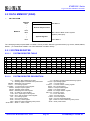
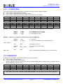
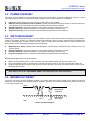
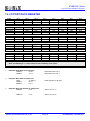
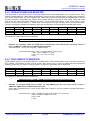
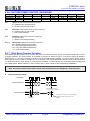
9.2 RFC APPLICATION CIRCUIT
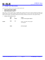
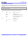
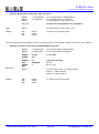
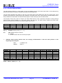
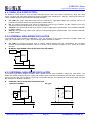
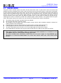
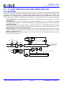
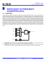
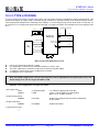
RFC application is configured a resistive device and a capacitor. Normally, the resistor is a sensor type device and the
capacitor is a static device. The connection diagram is as following. The resistor connects from Vdd to RFC channel,
and the capacitor connects from Vss to RFC channel. When RFC function actives, the internal RFC oscillation
generator makes the RFC channel oscillating. The frequency depends on R and C value.
RFCOUT
R1
R2
R3
R4
R5
RFC0
RFC1
RFC2
RFC3
RFC4
C1
C2
C3
C4
MCU
C5
VCC
GND
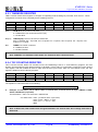
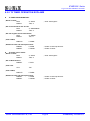
These RC circuits are switched by RFCH[2:0] bits of RFCM register. If one RFC input is selected, the other pins switch
to GPIO mode. Recommend set RFC0~RFC4 (P1.0~P1.4) as input floating. RFC digitally converting clock is output
from RFCOUT pin (P1.6) controlled by RFCOUT bit of RFC register.
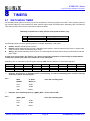
9.3 RFC OPERATION
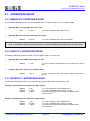
VDD
To T1 RFC Measurement Counter
(1) (2)
R
RFC
Oscillation
Generator
(2)
RFC Channel
C
(1)
VSS
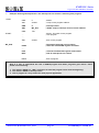
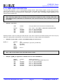
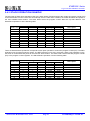
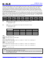
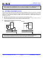
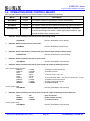
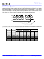
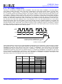
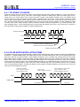
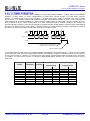
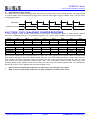
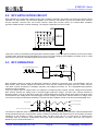
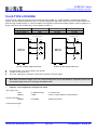
RFC operation is base on charge and discharge capacitor to obtain the converting clock. The RFCENB=1 turns on
RFC function. RFC channel charges the external RC circuit until the voltage level higher than ViH of RFC cahnnel.
Then RFC channel exchanges to discharge operation until voltage level under ViL. The charge/discharge operation
obtains the RFC oscillation.
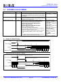
Loop (1) of above figure is charge mode. The capacitor is charged by RFC channel, and the voltage level increases.
RFC channel detects the voltage level to Schmitt trigger high-level voltage, and then RFC channel switches to
discharge mode. Loop (2) is discharge mode. RFC channel discharges and the voltage level starts to fall down. RFC
channel detects the voltage level to Schmitt trigger low-level voltage, and then RFC channel switches to charge mode.
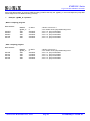
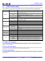
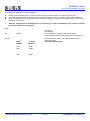
The result of charge and discharge switching is converted by RC oscillation control circuit and generate digitally clock.
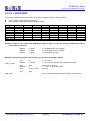
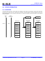
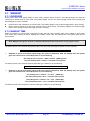
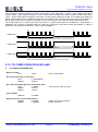
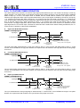
High Level of Schmitt trigger
RFC Input Signal
Low Level of Schmitt trigger
Discharge
Charge
VDD
RFC Clock & RFCOUT (RFC Output)
VSS
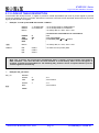
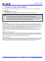
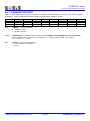
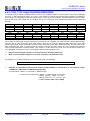
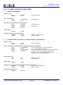
The reference capacitor value is steady. The RFC clock frequency value depends on resistance value and determines
charge and discharge rate. Using the RFC clocks of reference resistance and resistive sensor can measure the sensor
resistance by the frequency of RFC converting result. The RFC clock can be T1 clock source to measure RFC
converting value by frequency measurement and pulse width measurement. The RFC clock also can output to
RFCOUT pin (P1.6) when RFCOUT =1.
SONiX TECHNOLOGY CO., LTD
Page 99
Preliminary Version 0.1