1
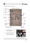
SIM5210
Debug Board
User Manual
Designed by SIMCOM Ltd,.
4th Jan 2007
SIM5210 Debug Board User Manual
Confidential
Designed by SIMCOM
Document Name:
SIM5210 Debug Board User Manual
Version:
Date:
Doc Id:
Status:
1.1
2007-06-29
SIM5210_debug_V1.1
General Notes
Simcom offers this information as a service to its customers, to support application and
engineering efforts that use the products designed by Simcom. The information provided is based
upon requirements specifically provided to Simcom by the customers. Simcom has not undertaken
any independent search for additional relevant information, including any information that may be
in the customer’s possession. Furthermore, system validation of this product designed by Simcom
within a larger electronic system remains the responsibility of the customer or the customer’s
system integrator. All specifications supplied herein are subject to change.
Copyright
This document contains proprietary technical information which is the property of SIMCOM
Limited., copying of this document and giving it to others and the using or communication of the
contents thereof, are forbidden without express authority. Offenders are liable to the payment of
damages. All rights reserved in the event of grant of a patent or the registration of a utility model
or design. All specification supplied herein are subject to change without notice at any time.
Copyright © SIMCOM Limited. 2006
SIM5210_Debug_V1.1
Page 2 of 15
SIM5210 Debug Board User Manual
Confidential
Designed by SIMCOM
Contents
Contents ............................................................................................................................................3
1 Introduction....................................................................................................................................5
1.1 Related documents ..............................................................................................................5
1.2 Terms and abbreviations......................................................................................................5
2 Product concept..............................................................................................................................6
2.1 The Debug Board key features at a glance..........................................................................6
3 Application interface......................................................................................................................6
3.1 Board view ..........................................................................................................................7
3.2 Interface description............................................................................................................9
SIM5210_Debug_V1.1
Page 3 of 15
SIM5210 Debug Board User Manual
Confidential
Designed by SIMCOM
Version history
Data
Version
Description of change
Author
2007-01-04
01.00
Origin
dingyiru
2007-06-29
1.1
Update the image of the board
dingyiru
SIM5210_Debug_V1.1
Page 4 of 15
SIM5210 Debug Board User Manual
Confidential
Designed by SIMCOM
1 Introduction
This document describes the structure of SIM5210 Debug Board, It also describes how to use this
board to support custom to use SIM5210 to design their applications
1.1 Related documents
Table 1: Related documents
SN
Document name
Remark
SIM5210_HD_V1.1
SIM5210 HARDWARE SPECIFICATION
1.2 Terms and abbreviations
Table 2: Terms and abbreviations
Abbreviation
Description
SIM5210_Debug_V1.1
Page 5 of 15
SIM5210 Debug Board User Manual
Confidential
Designed by SIMCOM
2 Product concept
The Debug board is designed for custom to design their applications by using the 3G module
SIM5210 easily .
All the functions of the SIM5210 can be used by this board. One can use UART, USB
interface to communicate with the SIM5210, and can design their camera phone by SIM5210,
There is one UART interface, one USB 2.0 interface, one Simcard interface , one T-FLASH
card interface, two camera interfaces, and four audio interface on the board.
One can connect the UART and the USB interface to a computer directly.
2.1 The Debug Board key features at a glance
Table 3: Debug board key features
Feature
Implementation
Power supply
1: Single supply voltage 6.0V – 9.0V at J13and J16
2: 3.5V~4.3V at J19
functions
z
z
z
z
z
z
z
z
UART interface
USB2.0 interface
SIMCARD interface
TFLASH interface.
Two sensor interface
Onkey
Keypad
Audio interface
3 Application interface
All hardware interfaces that connects SIM5210 to the customers’ cellular application platform is
through a 70-pin 0.5mm pitch board-to-board connector. Sub-interfaces included in this
board-to-board connector are described in detail in following chapters:
Electrical and mechanical characteristics of the board-to-board connector are specified in Chapter
6. There we also order information for mating connectors.
SIM5210_Debug_V1.1
Page 6 of 15
SIM5210 Debug Board User Manual
Confidential
Designed by SIMCOM
3.1 Board view
USB connector
Audio JACK
JTAG
PHONE ON
Level shift
Audio out
DB9 RS232
70 PIN B to B
UART
connect
interface
(cmos level)
USIM+TFLASH
HOLDER
DC in
DC-DC LM317
Reset switch
KEYPAD
SIM5210_Debug_V1.1
RGB sensor
YUV sensor
connector
connector
Page 7 of 15
SIM5210 Debug Board User Manual
Confidential
Designed by SIMCOM
Table 4:On Board Connector description
No
Name
1
J1
70PIN B to B connector, connect to SIM5210 module
2
J2
RGB sensor connector, An OV2640 2.0M sensor can be used
3
J3
USIM and T-FLASH card holder.
4
J4
No use
5
J5
YUV sensor connector, An OV7670 0.3M sensor can be used
6
J6
USB connector
7
J7
DC-DC out test point, connect this pin to J19 when use a
external DC power supply, you can use a 3.5V~4.3V DC
supply to J19 when you not use a external DC supply
8
J8
JTAG connector, for download firmware only
9
J9
Audio interface connector, MIC, receiver, speaker and line in
are in this connector, also the Phone on and a GPIO pin are in
this connector.
10
J10
UART connector. the UART interface is in CMOS level.
11
J11
DB9 UART interface. This can be connect to a PC directly
12
J12
Receiver +, connect to a receiver with the J14 together
13
J13
External DC supply input,
SIM5210_Debug_V1.1
Description
Page 8 of 15
SIM5210 Debug Board User Manual
Confidential
Designed by SIMCOM
14
J14
Receiver -, connect to a receiver with the J12 together
15
J15
no use
16
J16
GND ( for external DC power supply)
17
J17
Connect to DB9 connector DSR of J11
18
J18
Audio jack, for headset use.
19
J19
VABT input, if you don’t use the DC-DC circuit, you can supply
a 3.5V~4.3V DC supply to this pin directly
20
J20
MIC input PIN
3.2 Interface description
3.2.1 B to B connector J1
This 70 pin plug use to connect to SIM5210 module. The plug is AXK870145WG
which a product of NAIS.
3.2.2 RGB sensor connector J2
This 24PIN B to B socket is used to connect a RGB sensor ,the socket is made by HRS,
PIN24
PIN13
PIN12
PIN1
SIM5210_Debug_V1.1
Page 9 of 15
SIM5210 Debug Board User Manual
Confidential
Designed by SIMCOM
PIN LIST
PIN No
Define
PIN No
Define
1
NC
24
Y0
2
AGND
23
Y1
3
SIO_D
22
Y4
4
AVDD
21
Y3
5
SIO_C
20
Y5
6
RST
19
Y2
7
VSYNC
18
Y6
8
PWDN
17
PCLK
9
HREF
16
Y7
10
DVDD
15
AGND
11
IOVDD
14
Y8
12
Y9
13
XCLK
3.2.3 SIMCARD and T-FLASH card holder J3
J3 is a two connector in one package. the upstairs is SIMCARD holder. downstairs is
T-FLASH card holder
PIN16
PIN7
PIN14
Pin 1
Pin6
Note:the Pin No isn’t in sequence, detail description is in follow table.
SIM5210_Debug_V1.1
Page 10 of 15
SIM5210 Debug Board User Manual
Confidential
PIN No
Define
Designed by SIMCOM
PIN No
Define
1
SIMVCC
16
SW2
4
GND
15
SW1
2
SIMRST
7
TF-DATA2
5
SIMVPP
8
TF-DATA3
3
SIMCLK
9
TF-CMD
6
SIMIO
10
TF-VDD
11
TF-CLK
12
GND
13
TF-DATA0
14
TF-DATA1
3.2.4 J4 just for test use
3.2.5 YUV sensor connector J5
J5 is a 34pin B to B connector which produced by NAIS, the PART NO is
AXK834145WG
PIN18
PIN34
PIN17
SIM5210_Debug_V1.1
PIN1
Page 11 of 15
SIM5210 Debug Board User Manual
Confidential
PIN No
Define
Designed by SIMCOM
PIN No
Define
1
DGND
34
NC
2
PCLK
33
NC
3
NC
32
NC
4
NC
31
NC
5
RST
30
Y7
6
NC
29
Y6
7
NC
28
Y5
8
SIO_D
27
Y4
9
SIO_C
26
Y3
10
NC
25
Y2
11
NC
24
Y1
12
NC
23
Y0
13
PWDN
22
NC
14
NC
21
XCLK
15
IOVDD
20
AGND
16
AVDD
19
VSYNC
17
DVDD
18
HREF
3.2.6 USB connector J6
It is a normal 4Pin USB connector
3.2.7 SIM5210 DC supply input J7,J19
J7 is the DC-DC out , J19 is connected to J7 through a 0 resistor, if one want to use a
battery to supply the circuit, the resistor can be removed and connector the battery +to J19.
3.2.8 JTAG connector J8
JTAG connector is used to debug the SIM5210, or used to download firmware to the
SIM5210 when the firmware is damaged.
Note that one can download firmware through the USB connector except the loader
SIM5210_Debug_V1.1
Page 12 of 15
SIM5210 Debug Board User Manual
Confidential
Designed by SIMCOM
software in the SIM5210 is damaged.
3.2.9 Audio interface connector J9
PIN20
PIN2
PIN19
PIN1
PIN NO
DEFINE
PIN NO
DEFINE
1
SPK1
2
GPIO
3
GND
4
PHONE ON
5
SPK2
6
GND
7
GND
8
PCM_DOUT
9
LINE_IN_L
10
PCM_DIN
11
LINE_IN_R
12
PCM_CLK
13
GND
14
PCM_SYNC
15
MIC_P
16
GND
17
MIC_M
18
EAR_M
19
GND
20
EAR_P
3.2.10 UART interface J10
The odd pins of this connector is connected to the SIM5210 UART interface. The
level is CMOS level(VH=2.6V, VL<0.3V) .The even PINs is connected to J11 which is the
RS232 level UART.
When you want to use J11 connect to a PC, you must not connect the odd PINs to
even PINs.
SIM5210_Debug_V1.1
Page 13 of 15
SIM5210 Debug Board User Manual
Confidential
Designed by SIMCOM
PIN1
PIN19
PIN2
PIN NO
PIN20
DEFINE
PIN NO
DEFINE
1
UART_TXD
2
TXD
3
UART_CTS
4
CTS
5
UART_DCD
6
DCD
7
UART_RI
8
RI
9
UART_DTR
10
DTR
11
UART_RTS
12
RTS
13
UART_RXD
14
RXD
15
GND
16
GND
17
NC
18
NC
19
NC
20
NC
3.2.11 UART (RS232 level) interface J11
J11 is 9 PINs standard RS232 UART interface. It can be connected to a PC directly
SIM5210_Debug_V1.1
Page 14 of 15
SIM5210 Debug Board User Manual
Confidential
Designed by SIMCOM
PIN No
Define
1
UART_DCD (connect to PC DCD)
2
UART_RXD (connect to PC TXD)
3
UART_TXD (connect to PC RXD)
4
UART_DTR (connect to PC DSR)
5
GND
6
CONNECT TO J17
7
UART_RTS (connect to PC CTS)
8
UART_CTS (connect to PC RTS)
9
UART_RI
(DSR)
(connect to PC RI)
3.2.12 MIC/receiver interface J12,J14,J20
J12,J14 and J20 are solder mask ,One can connect the MIC AND a receiver to those
point ,note that the MIC’s polarity must be correct.
3.2.13 External DC supply connector J13,J16
One can connect these PIN to a DC regulator, the output voltage of the regulator shall
be large than 6Vand less than 35V
3.2.14 Headset connector J15,J18
J18 is a audio jack which has 6 pins .it has connected to a MIC and two speakers, the
speaker resistor should be a 32 OM
SIM5210_Debug_V1.1
Page 15 of 15