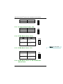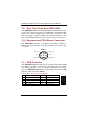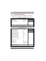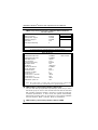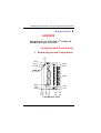
1
SBC84810 Series ® Pentium M All-in-One Capa Board with DualView display User’s Manual Disclaimers The information in this manual has been carefully checked and is believed to be accurate. Axiomtek Co., Ltd. assumes no responsibility for any infringements of patents or other rights of third parties which may result from its use. Axiomtek assumes no responsibility for any inaccuracies that may be contained in this document. Axiomtek makes no commitment to update or to keep current the information contained in this manual. Axiomtek reserves the right to make improvements to this document and/or product at any time and without notice. No part of this document may be reproduced, stored in a retrieval system, or transmitted, in any form or by any means, electronic, mechanical, photocopying, recording, or otherwise, without the prior written permission of Axiomtek Co., Ltd. CAUTION Danger of explosion if battery is incorrectly replaced.Replace only with the same or equivalent type To be recommended by the manufacturer. Dispose of used batteries according To the manufacturer’s instructions ©Copyright 2005 by Axiomtek Co., Ltd. All rights reserved. September 2005, Version A2 Printed in Taiwan ii ESD Precautions Integrated circuits on computer boards are sensitive to static electricity. To avoid damaging chips from electrostatic discharge, observe the following precautions: Do not remove boards or integrated circuits from their anti-static packaging until you are ready to install them. Before handling a board or integrated circuit, touch an unpainted portion of the system unit chassis for a few seconds. This helps to discharge any static electricity on your body. Wear a wrist-grounding strap, available from most electronic component stores, when handling boards and components. Trademarks Acknowledgments AXIOMTEK is a trademark of AXIOMTEK Co., Ltd. MS-DOS and Windows ’95 are trademarks of Microsoft Corporation. AWARD is a trademark of Award Software. Inc. IBM, PC/AT, PS/2, VGA are trademarks of International Business Machines Corporation. Intel and Pentium are trademarks of Intel Corporation. Winbond is a trademark of Winbond Electronics Corp. SMI is a trademark of Silicon Motion Inc. Other brand names and trademarks are the properties and registered brands of their respective owners. iii This page does not contain any information. iv Table of Contents Disclaimers............................................................................ii ESD Precautions..................................................................iii C h a p t e r 1..............................................................................1 Introduction ...............................................................................1 1.1 1.2 Specifications .......................................................2 Utilities Supported................................................4 C h a p t e r 2..............................................................................5 Jumpers and Connectors .........................................................5 2.1 2.2 2.3 Board Layout and Fixing Holes...........................5 Placement..............................................................6 Jumper Settings....................................................7 2.3.1 Audio Output Select Jumper: JP5...............................7 2.3.2 CMOS Clear Jumper: JP3 ............................................7 2.3.3 Compact Flash Power: JP4..........................................8 2.3.4 COM1 Mode Select: JP10 ...........................................8 2.3.5 COM2 Mode Select: JP9 .............................................8 2.3.6 COM2 Mode Select for RS-232/422/485: JP6/JP7/JP8...............................................................................8 2.3.7 LVDS Voltage Setting: JP2............................................9 2.4 2.4.1 2.4.2 2.4.3 2.4.4 2.4.5 2.4.6 2.4.7 2.4.8 2.4.9 2.4.10 Connectors..........................................................10 Enhanced IDE Interface Connector: CN6................10 Flat Panel Bezel Connector: CN10 ...........................11 VGA/Flat Panel Connector: VGA1, CN14................12 Parallel Port: CN5 .......................................................12 Power Input Connector: CN1 ....................................13 AC97 Interface Link Connector: CN8.......................14 Keyboard and PS/2 Mouse Connectors: CN13.......14 FDD Connector: CN16 ...............................................15 USB1~4 Connectors: CN7, CN12...............................15 Ethernet PJ-45 Connector: CN11 .............................16 Table of Contents v 2.4.11 Serial Port Interface: CN15, CN9..............................16 2.4.12 Compact Flash Connector: CN17 .............................18 2.4.13 Digital I/O Connector: CN18 ......................................20 2.4.14 LVDS Flat Panel Connector: CN2,CN4 .......................20 2.4.15 LVDS Power Connector: CN3 .....................................20 C h a p t e r 3............................................................................21 Hardware Description............................................................21 3.1 3.2 3.3 3.4 3.5 3.6 3.6.1 3.6.2 3.6.3 3.7 3.8 3.9 3.10 3.11 3.12 3.13 3.14 Microprocessors.................................................21 BIOS .....................................................................21 System Memory ..................................................21 I/O Port Address Map .........................................22 Interrupt Controller.............................................23 Display Interface .................................................24 Graphic Controller .....................................................24 Features ......................................................................24 VGA/Flat Panel Connectors......................................25 Floppy Disk Controller .......................................28 Parallel Port Interface.........................................29 Real Time Clock and CMOS RAM......................30 Keyboard and PS/2 Mouse Connector..............30 USB Connector ...................................................30 Ethernet RJ-45 Connector .................................31 Audio Connector.................................................32 Compact Flash™ Socket (CN17) .......................33 C h a p t e r 4............................................................................36 Award BIOS Utility................................................................36 4.1 4.2 4.3 4.4 vi Entering Setup ....................................................36 Control Keys .......................................................37 Getting Help ........................................................37 The Main Menu....................................................38 Table of Contents 4.5 4.6 4.7 4.8 4.9 4.10 4.11 4.12 4.13 4.14 4.15 4.16 4.17 Standard CMOS Setup Menu .............................39 Advanced BIOS Features...................................42 Advanced Chipset Features ..............................47 Integrated Peripherals........................................49 Power Management Setup .................................54 PnP/PCI Configuration Setup ............................59 PC Health Status.................................................62 Frequency/Voltage Control................................63 Load Fail-Safe Defaults ......................................64 Load Optimized Defaults....................................65 Set Supervisor/User Password .........................66 Save & Exit Setup ...............................................67 Exit Without Saving ............................................68 A p p e n d i x A ......................................................................70 Watch Dog Timer ....................................................................70 Watchdog Timer Setting ....................................................70 Using the Watchdog Function...........................................71 A p p e n d i x B ......................................................................73 Jumpers and Connectors .......................................................73 1. Board Layout and Fixing Holes....................................73 COM3 Mode Select: JP2........................................................75 COM4 Mode Select: JP3........................................................76 LVDS Voltage Setting : JP1.....................................................76 Table of Contens vii SBC84810 Pentium® M All-in-One Capa Board User’s Manual Chapter 1 Introduction The SBC84810 is an Intel ® Pentium ® M/Celeron™ M CPU equipped Capa board with graphics, Fast Ethernet and audio interface. Designed with the space-limited applications in mind, the SBC84810 is practically the finest embedded Pentium ® M board that exists. Using a standardized format conforming to the size of a 3.5” Hard Disk drive, SBC84810 Series adapt an Intel ® low power consumption Pentium ® M microprocessors. To simplify system integration, it packs provisions such as super I/Os, UXGA, LCD, Ethernet, solid state disk, all on a single board. Unique embedded features such as 2 serial ports (1 x RS-232, 1 x RS-232/422/485) (optional 2* RS-232 ports via stacking kit) with +5V/12V power capability and that allow adoption of an extensive array of PC peripherals. The industrial-grade construction of SBC84810 series allows your system to endure the continuous operation in hostile environments where stability and reliability are basic requirements. System dependability of SBC84810 series are enhanced by its built-in watchdog timer, a special industrial feature not commonly seen on other motherboards. Introduction 1 SBC84810 Pentium® M All-in-One Capa Board User’s Manual Designed for the professional embedded developers, the Pentium ® M embedded board SBC84810 Series is virtually the ultimate one-step solution for embedded system applications. 1.1 Specifications Intel ® Pentium ® M 1.1/1.4GHz and Celeron ® M 600M/1GHz z CPU: z System Chipset: Intel ® 852GM + ICH*4 z Bus Clock: 400MHz z BIOS: Phoenix-Award BIOS, Y2K compliant 4Mbit Flash, DMI, Plug and Play SmartView for multiple LCD type selection, display mode option and application extension features RPL/PXE Ethernet Boot ROM “Load Optimized Default” to backup customized Setting in the BIOS flash chip to prevent from CMOS battery fail z System Memory: One 200-Pin DDR SODIMM socket Maximum DDR of up to 1GB DDR266 z L2 Cache: integrated in CPU z Onboard IDE: 1 parallel ATA-100 PATA-100 as PIO Mode 0-4, DMA Mode 0-2 and Ultra DMA/33/66/100 z Compact Flash Socket: One Compact Flash Type II Socket z Onboard Multi I/O: One floppy port 1 x RS-232 1 x RS-232/422/485 Optional 2*RS-232 ports via AX93200 stacking kit 2 Introduction SBC84810 Pentium® M All-in-One Capa Board User’s Manual z USB Interface: 4 USB ports with fuse protection and complies with USB Spec. Rev. 2.0 z Real Time Clock: z Watchdog Timer: Integrate Intel ® ICH*4 1~255 seconds; up to 255 levels z Graphics/Streaming: Integrate Intel 852GM GMCH Unified Memory Architecture shares system memory up to 32MB Single display mode maximum resolutions: z z CRT: 2048 x 1536@ 75Hz LVDS LCD: 1600 x 1200 DualView display mode: CRT: 2048 x 1536@ 75Hz LVDS LCD: 1600 x 1200 LCD backlight control supported Optional Dual LVDS LCD via stacking kit AX93200 with Chrontel CH7305 converter Ethernet: z ® Realtek 8100C PCI Bus 10/100M Base-T Wake On LAN (via ATX power supply) Equipped with RJ-45 interface Optional with Realtek RTL8110S for 10/100/1000Base-T 2 nd Ethernet supported by optional stacking kit AX93201 Audio: Realtek ALC202A AC’97 codec audio Amplify for speaker-out with 2.5W for each channel MIC-in, Line-in, Line-out/Speaker-out (jumper selectable) Power Management: Introduction ACPI (Advanced Configuration and Power Interface) 3 SBC84810 Pentium® M All-in-One Capa Board User’s Manual z Form Factor: 3.5” hard disk drive form factor NOTE: 1.2 Specifications are subject to change without notice. Utilities Supported z Chipset Driver z Ethernet Driver z VGA Drivers z Audio Drivers 4 Introduction SBC84810 Pentium® M All-in-One Capa Board User’s Manual Chapter 2 Jumpers and Connectors 141.66 143.05 121.16 94.32 100.66 72.52 50.72 30.99 Board Layout and Fixing Holes 4.45 8.89 11.68 2.1 104.65 98.37 98.37 94.74 74.81 66.29 66.09 63.12 51.43 44.20 34.54 25.10 3.18 0.00 Jumpers and Connectors 143.05 146.05 124.00 100.00 84.00 51.89 27.66 0.00 8.89 3.18 5 SBC84810 Pentium® M All-in-One Capa Board User’s Manual 2.2 6 Placement Jumpers and Connectors SBC84810 Pentium® M All-in-One Capa Board User’s Manual 2.3 Jumper Settings The SBC84810 Series is configured to match the needs of your application with the proper jumper settings. The table below is a summary of all the jumpers and their corresponding functions onboard the SBC84810 Series. The succeeding tables show the correct jumper settings for the onboard devices. SBC84810 Jumper setting: Jumper Default Setting Jumper Setting JP6 LVDS Voltage select: 3.3V Clear CMOS Setting: Normal Compact Flash Power Select: 3.3V Audio Line Out/Speaker Out: Line Out COM2 Mode Select: RS-232 Short Short Short Short Short JP7 COM2 Mode Select: RS-232 Short 3-5,4-6 JP8 COM2 Mode Select: RS-232 Short 3-5,4-6 JP9 COM2 Mode Select JP10 COM1 Mode Select Short Short Short Short JP2 JP3 JP4 JP5 CN9 Pin 1: DCD CN9 Pin 8: RI CN15 Pin 1: DCD CN15 Pin 8: RI 1-2 1-2 1-2 1-3, 2-4 1-2 3-5 4-6 3-5 4-6 2.3.1 Audio Output Select Jumper: JP5 Options Line Out Speaker Out JP5 Settings Short 1-3, 2-4 (default) Short 3-5, 4-6 2 4 6 1 3 5 2.3.2 CMOS Clear Jumper: JP3 Options Jumpers and Connectors Settings JP3 7 SBC84810 Pentium® M All-in-One Capa Board User’s Manual Normal Clear CMOS Short 1-2 (default) Short 2-3 1 2 3 2.3.3 Compact Flash Power: JP4 Options JP4 Settings Short 1-2(default) Short 2-3 3.3V 5V 1 2 3 2.3.4 COM1 Mode Select: JP10 COM1 JP10 *Pin 1=DCD *Pin 1=5V Short 3-5(default) Short 1-3 *Pin 8=RI *Pin 8=+12V Short 4-6(default) Short 2-4 JP10 格式化: 項目符號及編號 2.3.5 COM2 Mode Select: JP9 COM2 JP9 *Pin 1=DCD *Pin 1=5V Short 3-5(default) Short 1-3 *Pin 8=RI *Pin 8=+12V Short 4-6(default) Short 2-4 JP9 2.3.6 COM2 Mode Select for RS-232/422/485: JP6/JP7/JP8 8 Jumpers and Connectors SBC84810 Pentium® M All-in-One Capa Board User’s Manual JP7 JP8 RS-232 (default) COM2 1-2 JP6 3-5, 4-6 3-5, 4-6 RS-422 3-4, 7-8 1-3, 2-4 1-3, 2-4 RS-485 5-6, 7-8 1-3, 2-4 1-3, 2-4 JP6 JP7/JP8 6 5 5 3 4 3 2 1 8 7 6 4 2 1 2.3.7 LVDS Voltage Setting: JP2 VDDM 5V Short 2-3 3.3V Short 1-2(default) Jumpers and Connectors JP2 Settings 1 2 3 9 SBC84810 Pentium® M All-in-One Capa Board User’s Manual 2.4 Connectors The connectors allow the CPU card to connect with other parts of the system. Some problems encountered by your system may be a result from loose or improper connections. Ensure that all connectors are in place and firmly attached. The following table lists the function of each connector on the SBC84810 Series. Their corresponding pin assignments are described in Chapter 3. Connectors Label Connectors Label Power Connector CN1 LAN1 RJ-45 Connector CN11 LVDS Channel B Connector CN2 USB Port0 & Port1 Connector CN12 LVDS Voltage Connector CN3 CN13 LVDS Channel A Connector CN4 6-Pin Mini Dim Keyboard/Mouse Connector VGA Connector Printer Port Connector CN5 Serial Port1 Connector CN15 Parallel IDE Connector CN6 FDD Connector CN16 USB Port2 & Port3 Connector CN7 Compact Flash Connector CN17 Audio Connector CN8 Digital I/O CN18 Serial Port2 Connector CN9 Extension Slot J1 CN10 DDR SO-DIMM DIMM1 Front Panel Bezel Connector 2.4.1 CN14 Enhanced IDE Interface Connector: CN6 The SBC84810 includes a PCI bus enhanced IDE controller that can support master/slave mode and post write transaction mechanisms with 64-byte buffer and master data transaction. 44-pin IDE Interface Connector: Pin 10 Description Pin Description Pin Description 1 Reset # 2 GND 3 Data 7 4 Data 8 5 Data 6 6 Data 9 7 Data 5 8 Data 10 9 Data 4 10 Data 11 11 Data 3 12 Data 12 Jumpers and Connectors SBC84810 Pentium® M All-in-One Capa Board User’s Manual 2.4.2 13 Data 2 14 Data 13 15 Data 1 16 Data 14 17 Data 0 18 Data 15 19 GND 20 No connector 21 No connector 22 GND 23 IOW # 24 GND 25 IOR # 26 GND 27 IOCHRDY 28 No connector 29 No connector 30 GND-Default 31 Interrupt 32 No connector 33 SA1 34 No connector 35 SA0 36 SA2 37 HDC CS0 # 38 HDC CSI # 39 HDD Active # 40 GND 41 VCC 42 VCC 43 GND 44 N.C Front Panel Bezel Connector: CN10 Power LED This 3-pin connector, designated at Pins 1 and 5 of CN10, connects the system power LED indicator to its respective switch on the case. Pin 1 is +, and pin 5 is assigned as -. The Power LED lights up when the system is powered ON. External Speaker and Internal Buzzer Connector Pins 2, 4, 6, and 8 of CN10 connect to the case-mounted speaker unit or internal buzzer. Short pins 4-6 when connecting the CPU card to an internal buzzer. When connecting an external speaker, set these jumpers to Open and install the speaker cable on pin 8 (+) and pin 2 (-). ATX Power On/Off Button This 2-pin connector, designated at Pins 9 & 10 of CN10, connects the ATX power button of the front panel to the Jumpers and Connectors 11 SBC84810 Pentium® M All-in-One Capa Board User’s Manual SBC84810 CPU card - allowing user to control the power on/off state of the ATX power supply. System Reset Switch Pins 11 & 12 of CN10 connect to the case-mounted reset switch and allow rebooting of your computer instead of turning OFF the power switch. This is a preferred method of rebooting in order to prolong the life of the system’s power supply. HDD Activity LED This connector extends to the hard drive activity LED on the control panel. This LED will flash when the HDD is being accessed. Pins 15 & 16 of CN10 connect the hard disk drive and the front panel HDD LED. Pins 15 is -, and pin 16 is assigned as +. Keyboard Lock Pins 13 and 14 of CN10 are Keyboard Lock setting. Short the Pins 13 and 14 for Keyboard Lock. 2.4.3 VGA Connector: CN14 The SBC84810 has three connectors that support CRT VGA and flat panel displays, individually or simultaneously. VGA1 is a slim type 15-pin D-Sub connector commonly used for the CRT VGA display, Configuration of the VGA interface is done via the software utility and no jumper setting is required. The following two tables are the pin assignments for the CRT/VGA connector and the flat panel connector. VGA1: CRT/VGA Connector Pin Assignment Pin Description Pin Description Pin Description 1 Red 2 Green 3 Blue 4 N/A 5 GND 6 AGND 7 AGND 8 AGND 9 N/A 10 GND 11 N/A 12 DDC DAT 13 Horizontal Sync 14 Vertical Sync 15 DDC CLK 2.4.4 Parallel Port: CN5 The SBC84810 has a multi-mode parallel port, CN5, to support: 12 Jumpers and Connectors SBC84810 Pentium® M All-in-One Capa Board User’s Manual z Standard mode: IBM PC/XT, PC/AT and PS/2™ compatible with bi-directional parallel port z Enhanced mode: Enhance parallel port (EPP) compatible with EPP 1.7 and EPP 1.9 (IEEE 1284 compliant) z High speed mode: Microsoft and Hewlett Packard extended capabilities port (ECP) IEEE 1284 compliant The address select of the onboard parallel port in LPT1 (3BCH) or disabled is done by BIOS CMOS setup. Pin Description Pin Description 1 Strobe# 2 Auto Form Feed# 1 2 3 Data 0 4 Error# 3 4 5 Data 1 6 Initialize# 5 6 Printer Select In# 7 9 8 10 11 12 13 15 14 16 7 Data 2 8 9 Data 3 10 GND 11 Data 4 12 GND 13 Data 5 14 GND 15 Data 6 16 GND 17 Data 7 18 GND 17 19 18 20 19 Acknowledge# 20 GND 21 22 23 25 24 26 21 Busy 22 GND 23 Paper Empty# 24 GND 25 Printer Select 26 NC 2.4.5 Power Input Connector: CN1 The following table is the pin assignment for the standard power supply with both 5V and 12V inputs. Pin Description Jumpers and Connectors CN1 13 SBC84810 Pentium® M All-in-One Capa Board User’s Manual 2.4.6 1 +5V 2 GND 3 +12V 4 SB5V 5 PS_ON 6 -12V 7 GND 8 +5V AC97 Interface Link Connector: CN8 The SBC84810 supports audio interface. CN8 is a 10pin-header connector commonly used for the audio. CN8 2 1 2.4.7 3 4 5 6 7 9 8 10 Keyboard and PS/2 Mouse Connectors: CN13 The SBC84810 provides a keyboard and Mouse interface. CN13 is a DIN connector for PS/2 keyboard Connection VIA “Y” Cable CN13 Mouse Clock Keyboard Clock 6 VCC Mouse Data 14 5 4 3 2 1 GND Keyboard Data Jumpers and Connectors SBC84810 Pentium® M All-in-One Capa Board User’s Manual 2.4.8 FDD Connector: CN16 The SBC84810 provides a 26-pin FCC Z.I.F. type connector, and the general output supports a single floppy drives. The floppy drive could be any one of the following types: 3.5" 720KB or 1.44MB/2.88MB. CN16: FDD Connector Pin Assignment Pin Description Pin Description 1 +5V 14 STEP 2 INDEX 15 GND 3 +5V 16 WDATA 4 DRIVE0 17 GND 5 +5V 18 WGATE 6 DSKCHG 19 GND 7 No connector 20 TRK0 8 No connector 21 GND 9 No connector 22 WPT 10 MOTOR ON 23 GND 11 No connector 24 RDATA 12 DIR 25 GND 13 No connector 26 HDSEL 2.4.9 USB1~4 Connectors: CN7, CN12 The SBC84810 Series features four Universal Serial Bus (USB) connectors as USB 2.0 compliant (480Mbps) that can adapt any USB peripherals, such as monitor, keyboard and mouse etc. The SBC84810 Series has a box-header connectors (CN7) and two USB connectors (CN12). CN7: USB Connector Pin Assignment Pin 1 3 5 7 9 Description VCC D0D0+ Ground (GND) Ground (GND) Jumpers and Connectors Pin 2 4 6 8 10 Description VCC D1D1+ Ground (GND) Ground (GND) 1 2 3 4 5 6 7 9 8 10 15 SBC84810 Pentium® M All-in-One Capa Board User’s Manual CN12: USB Connector Pin Assignment Pin 1 2 3 4 Signal Name USB USB USB USB Vcc + GND 2.4.10 Ethernet PJ-45 Connector: CN11 The RJ-45 connector is used for Ethernet. To connect the SBC84810 to a 100/10 Base-T hub, just plug one end of the cable into the CN11 connect the other end of the cable to a 1000/100/10-Base-T hub. 2.4.10.1 Pin Assignment CN11: RJ-45 Connector Pin Assignment Pin Signal 1 Tx+(Data transmission positive) 2 Tx-(Data transmission negative) 3 Rx+(Data reception positive) 4 RJ45 termination 5 RJ45 termination 6 Rx- (Data reception negative) 7 RJ45 termination 8 RJ45 termination 1 2 3 4 5 6 7 8 RJ-45 2.4.11 Serial Port Interface: CN15, CN9 The SBC84810 Series has two onboard serial ports, COM2 are RS-232 and COM2 is RS-232/422/485, selectable with auto flow control features. All two ports +5V/12V power capability on DCD and RI, depending jumper setting(See Section 2.3.4 and 2.3.5). 16 COM1, jumper feature on the Jumpers and Connectors SBC84810 Pentium® M All-in-One Capa Board User’s Manual 2.4.11.1 COM1 Port Connector: CN15 The connector, COM 1, is a DB-9 connector, and the following table shows the pin assignments of this connector. Pin Signal Name 1 DCD, Data carrier detect 2 RXD, Receive data 3 TXD, Transmit data 4 DTR, Data terminal ready 5 GND, ground 6 DSR, Data set ready 7 RTS, Request to send 8 CTS, Clear to send 9 RI, Ring indicator COM1 2.4.11.2 COM2 Port Connectors: CN9 The RS-232 pin assignments are listed on the following table. Pin 1 Description Data Carrier (DCD) Pin Detect 2 Description Data Set Ready (DSR) 3 Receive Data (RXD) 4 Request to Send (RTS) 5 Transmit Data (TXD) 6 Clear to Send (CTS) 7 Data Terminal (DTR) 8 Ring Indicator (RI) 9 Ground (GND) Ready Jumpers and Connectors 10 CN9 1 2 3 4 5 6 7 9 8 10 NC 17 SBC84810 Pentium® M All-in-One Capa Board User’s Manual The RS-422/485 pin assignments for COM2 are listed below. Pin # Signal Name R2-422 RS-485 1 TX- DATA- 2 No connector No connector 3 TX+ DATA+ 4 No connector No connector 5 RX+ No connector 6 No connector No connector 7 RX- No connector 8 No connector No connector 9 GND GND 10 No connector No connector 2.4.12 Compact Flash Connector: CN17 The SBC84810 Series is equipped with a CompactFlash disk socket on the solder side and it supports the IDE2 interface CompactFlash disk card. The socket itself is specially designed to prevent any incorrect installation of the CompactFlash disk card. When installing or removing the CompactFlash disk card, make sure the system power is off. The CompactFlash disk card is defaulted as the E: or F: disk drive in the PC system. 2.4.13 Digital I/O Port (DIO): CN18 The board is equipped a digital I/O connector CN18 that meets a system customary automation control needs. The digital I/O can be configured to control the cash drawer, or to sense the warning signal of an Uninterrupted Power System (UPS), or to perform the store security control. The digital I/O is controlled via software programming. Digital I/O Connector: CN18 18 Jumpers and Connectors SBC84810 Pentium® M All-in-One Capa Board User’s Manual Pin Signal DIO In 0 DIO In 1 GND Pin 1 3 5 2 4 6 Signal DIO Out 0 DIO Out 1 DIO Out 2 7 GND 8 DIO Out 3 8 7 6 5 4 3 2 1 Digital I/O Software Programming The Digital I/O on the board is not an isolated type. Output Address Bit Output Address Bit Out-1 40B8h 5 In-0 40B8h 0 Out-2 40B8h 6 In-1 40B8h 1 Out-3 40B8h 7 Out-0 40B8h 4 2.4.14 Connector for LVDS Flat Panel: CN2, CN4 CN4 Channel A Pin 1 Deception Pin VCCM 2 Deception VCCM 3 VCCM 4 VCCM 5 DA0- 6 DA3- 7 DA0+ 8 DA3+ 9 GND 10 GND 11 DA1- 12 CLKA- 13 DA1+ 14 CLKA+ 15 GND 16 GND 17 DA2- 18 GND 19 DA2+ 20 GND CN2 Channel B Pin 1 Deception Pin VCCM 2 Deception VCCM 3 VCCM 4 VCCM 5 DB0- 6 DB3- 7 DB0+ 8 DB3+ Jumpers and Connectors 19 SBC84810 Pentium® M All-in-One Capa Board User’s Manual 9 GND 10 GND 11 DB1- 12 CLKB- 13 DB1+ 14 CLKB+ 15 GND 16 GND 17 DB2- 18 GND 19 DB2+ 20 GND 2.4.15 LVDS Power Connector: CN3 CN3 is a Hirose DF13-5P- 1.25V(50) connector, the match side connector is DF13-5S-1.25C Pin 20 Signal CN3 1 +12VM1 1 2 VCC (+5V) 2 3 +12VM1 3 4 ENABLE 4 5 GND 5 Jumpers and Connectors SBC84810 Pentium® M All-in-One Capa Board User’s Manual Chapter 3 Hardware Description 3.1 Microprocessors The SBC84810 Series supports Intel® Celeron™ M and Pentium® M CPUs. Systems based on these CPUs can be operated under Windows 2000/XP and Linux environments. The system performance depends on the microprocessor installed onboard. Make sure all settings are correct for the installed microprocessor to prevent any damage to the CPU. 3.2 BIOS System BIOS used on the SBC84810 Series is Phoenix-Award Plug and Play BIOS. The SBC84810 Series contains a single 4Mbit Flash. 3.3 System Memory The SBC84810 Series industrial CPU card supports one 200pin DDR SODIMM socket for a maximum memory of 1GB DDR SDRAMs. The memory module can come in sizes of 64MB, 128MB, 256MB, 512MB and 1GB. Hardware Description 21 SBC84810 Pentium® M All-in-One Capa Board User’s Manual 3.4 I/O Port Address Map The Intel® Pentium® M/Celeron™ M CPU communicates via I/O ports. It has a total of 1KB port addresses available for assignment to other devices via I/O expansion cards. Address 000-01F DMA controller #1 020-03F Interrupt controller #1 040-05F Timer 060-06F Keyboard controller 070-07F Real time clock, NMI 080-09F DMA page register 0A0-0BF Interrupt controller #2 0C0-0DF 22 Devices DMA controller #2 0F0 Clear math coprocessor busy signal 0F1 Reset math coprocessor 0F8-0FF Math processor 1F0-1F8 Fixed disk controller 250-25F HR I/O 300-31F Prototype card 380-38F SDLC #2 3A0-3AF SDLC #1 3B0-3BF MDA video card (including LPT1) 3C0-3CF EGA card 3D0-3DF CGA card 3F0-3F7 Floppy disk controller 3F8-3FF Serial port #1 (COM1) 3E8-3EF Serial port #3 (COM3) 2F8-2FF Serial port #2 (COM2) 2E8-2EF Serial port #4 (COM4) 3F0-3FF Super I/O Hardware Description SBC84810 Pentium® M All-in-One Capa Board User’s Manual 3.5 Interrupt Controller The SBC84810 Series is a 100% PC compatible control board. It consists of 16 interrupt request lines. Four out of the sixteen can either be programmable. The mapping list of the 16 interrupt request lines is shown on the following table. NMI Parity check error IRQ0 System timer output IRQ1 Keyboard IRQ2 Interrupt rerouting from IRQ8 through IRQ15 IRQ3 Serial port #2 IRQ4 Serial port #1 IRQ5 Reserved IRQ6 Floppy disk controller IRQ7 Parallel port #1 IRQ8 Real time clock IRQ9 Reserved IRQ10 Serial port #3 IRQ11 Serial port #4 IRQ12 PS/2 Mouse IRQ13 Math coprocessor IRQ14 Primary IDE channel IRQ15 Secondary IDE Channel Hardware Description 23 SBC84810 Pentium® M All-in-One Capa Board User’s Manual 3.6 Display Interface 3.6.1 Graphic Controller The 852GM provides a highly integrated graphics accelerator delivering high performance 2D, 3D, and video capabilities. With its interfaces to UMA using a DVMT configuration, an analog display (CRT port), a LVDS port for digital LCD connection and optional second LVDS LCD interface (via Chrontel CH7305 converter on AX93200), the 852GM can provide a complete graphics solution. The 852GM also provides 2D hardware acceleration for block transfers of data (BLTs). Performing these common tasks in hardware reduces CPU load, and thus improves performance. High bandwidth access to data is provided through the system memory interface. The 852GM uses Tiling architecture to increase system memory efficiency and thus maximize effective rendering bandwidth. The Intel 852GM GMCH improves 3D performance and quality with 3D Zone rendering technology. The Intel 852GM GMCH also supports Video Mixer rendering and Bi-Cubic filtering. 3.6.2 Features z z 24 The SBC84810 adapts Intel 852GM GMCH provides three display ports, one analog and two digital. With these interfaces, the GMCH can support for a progressive scan analog monitor, a dedicated single/dual channel LVDS LCD panel and a converted LVDS LCD interface through DVO channel. Each port can transmit data according to one or more protocols. The data that is sent out the display port is selected from one of the two possible sources, Pipe A or Pipe B. Intel 852GM GMCH has an integrated 350-MHz, 24-bit RAMDAC that can directly drive a progressive scan analog monitor pixel resolution up to 2048 x 1536 at 75-Hz refresh. The Analog display port can be driven by Pipe A or Pipe B. Hardware Description SBC84810 Pentium® M All-in-One Capa Board User’s Manual The Intel 852GM GMCH has an integrated dual channel LFP Transmitter interface to support LVDS LCD panel resolutions up to UXGA. The display pipe provides panel up-scaling to fit a smaller source image onto a specific native panel size, as well as provides panning and centering support. The LVDS port is only supported on Pipe B. The LVDS port can only be driven by Pipe B, either independently or simultaneously with the Analog Display port. Spread Spectrum Clocking is supported: center and down spread support of 0.5%, 1%, and 2.5% utilizing an external SSC clock. z 3.6.3 VGA Connectors The SBC84810 Series has one connector that supports CRT/ VGA. CN14 is slim type D-sub connector used for the CRT VGA display, and CN2 & CN4 are Hirose DF-13 20pin connector for LVDS Interface LCD. CN4 for Channel 1, CN2 for channel 2.CN3 is inverter connector for LCD to support the system LCD backlight control with OS and driver independent. CN14: CRT/VGA Connector Pin Assignment Pin Description Pin Description Pin Description 1 Red 2 Green 3 Blue 4 N/A 5 GND 6 AGND 7 AGND 8 AGND 9 N/A 10 GND 11 N/A 12 DDC DAT 13 Horizontal Sync 14 Vertical Sync 15 DDC CLK Hardware Description 25 SBC84810 Pentium® M All-in-One Capa Board User’s Manual CN2/CN4: Hirose Connector for LVDS Flat Panel CN4 Channel A Pin Deception 1 VCCM 3 5 Pin Deception 2 VCCM VCCM 4 VCCM DA0- 6 DA3- 7 DA0+ 8 DA3+ 9 GND 10 GND 11 DA1- 12 CLKA- 13 DA1+ 14 CLKA+ 15 GND 16 GND 17 DA2- 18 GND 19 DA2+ 20 GND CN2 Channel B Pin Deception Pin Deception 1 VCCM 2 VCCM 3 VCCM 4 VCCM 5 DB0- 6 DB3- 7 DB0+ 8 DB3+ 9 GND 10 GND 11 DB1- 12 CLKB- 13 DB1+ 14 CLKB+ 15 GND 16 GND 17 DB2- 18 GND 19 DB2+ 20 GND CN3: Hirose Connector for Inverter Pin 26 Signal 1 +12VM1 2 VCC (+5V) 3 +12VM1 4 ENABLE 5 GND Hardware Description SBC84810 Pentium® M All-in-One Capa Board User’s Manual Hardware Description 27 SBC84810 Pentium® M All-in-One Capa Board User’s Manual 3.7 Floppy Disk Controller The SBC84810 Series provides a 26-pin FCC Z.I.F. type connector, CN16 for support of a single floppy drives. The floppy drive could be any one of the following types: 3.5" 720KB or 1.44MB/2.88MB. CN16: FDD Connector Pin Assignment Pin 1 2 3 4 5 6 7 8 9 10 11 12 13 28 Description +5V INDEX +5V DRIVE0 +5V DSKCHG No connector READY HDOUT MOTOR ON No connector DIR HDSEL Pin 14 15 16 17 18 19 20 21 22 23 24 25 26 Description STEP GND WDATA GND WGATE GND TRK0 GND WPT GND RDATA GND SIDE0 Hardware Description SBC84810 Pentium® M All-in-One Capa Board User’s Manual 3.8 Parallel Port Interface The SBC84810 Series has one onboard parallel port, LPT1. LPT1 has one 26-pin header connector. The onboard PRN of SBC84810 Series is a multi-mode parallel port supporting: z Standard mode: IBM PC/XT, PC/AT and PS/2™ compatible with bidirectional parallel port z Enhanced mode: Enhance parallel port (EPP) compatible with EPP 1.7 and EPP 1.9 (IEEE 1284 compliant) z High speed mode: Microsoft and Hewlett Packard extended capabilities port (ECP) IEEE 1284 compliant The address selection of the onboard parallel port, in LPT1 (378H) or disabled, is configured within the BIOS CMOS setup utility. CN5: Parallel Port Connector Pin Assignment Pin 1 2 3 4 5 6 7 8 9 10 11 12 13 Description Pin Strobe# Data 0 Data 1 Data 2 Data 3 Data 4 Data 5 Data 6 Data 7 Acknowledge# Busy Paper Empty# Printer Select 14 Hardware Description 15 16 17 18 19 20 21 22 23 24 25 26 Description Auto Form Feed# Error# Initialize# Printer Select In# GND GND GND GND GND GND GND GND No connector 1 2 3 4 5 6 7 9 8 10 11 13 12 15 17 19 14 16 18 20 21 22 23 25 24 26 29 SBC84810 Pentium® M All-in-One Capa Board User’s Manual 3.9 Real Time Clock and CMOS RAM The SBC84810 Series contains 63000EB Integrated Real Time Clock (RTC) and 128 bytes of CMOS RAM. The CMOS RAM stores the system configuration information entered via the SETUP program. A battery keeps the stored information on the RTC and CMOS RAM active when system power is turned off. 3.10 Keyboard and PS/2 Mouse Connector The SBC84600 provides a keyboard and Mouse interface. CN13 is a DIN connector for PS/2 keyboard Connection VIA “Y” Cable CN13 Mouse Clock Keyboard Clock 5 6 VCC 4 3 Mouse Data 2 GND Keyboard Data 1 3.11 USB Connector The SBC84810 Series features four Universal Serial Bus (USB) connectors as USB 2.0 compliant (480Mbps) that can adapt any USB peripherals, such as monitor, keyboard and mouse etc. The SBC84810 Series has a box-header connectors (CN7) and two USB connectors (CN12). CN7: USB Connector Pin Assignment Pin 1 3 5 7 9 30 Description VCC D0D0+ Ground (GND) Ground (GND) Pin 2 4 6 8 10 Description VCC D1D1+ Ground (GND) Ground (GND) 1 2 3 4 5 6 7 9 8 10 Hardware Description SBC84810 Pentium® M All-in-One Capa Board User’s Manual CN12: USB Connector Pin Assignment Pin 1 2 3 4 Signal Name USB USB USB USB Vcc + GND 3.12 Ethernet RJ-45 Connector The RJ-45 connector is used for Ethernet. To connect the SBC84810 to a 100/10 Base-T hub, just plug one end of the cable into the CN11 and connect the other end of the cable to a 1000/100/10-Base-T hub. LAN1: RJ-45 Connector Pin Assignment Pin Signal 1 Tx+ (Data transmission positive 2 Tx(Data negative) 3 Rx+(Data reception positive) 4 RJ45 termination 5 RJ45 termination 6 Rx- (Data reception negative) 7 RJ45 termination 8 RJ45 termination Hardware Description transmission 1 2 3 4 5 6 7 8 RJ-45 31 SBC84810 Pentium® M All-in-One Capa Board User’s Manual 3.13 Audio Connector The SBC84810 supports audio interface. CN8 is a 10pinheader connector commonly used for the audio. CN8 Pin Signal Pin Signal 1 3 5 7 9 32 MIC-IN Line In L Line In R Audio Out L Audio Out R 2 4 6 8 10 GND GND GND GND GND 1 2 3 4 5 6 7 9 8 10 Hardware Description SBC84810 Pentium® M All-in-One Capa Board User’s Manual 3.14 Compact Flash™ Socket (CN17) The SBC84810 Series is equipped with a Compact Flash disk type-II socket on the solder side and it supports the IDE interface Compact Flash disk card with DMA mode supported. The socket itself is especially designed to prevent any incorrect installation of the Compact Flash disk card. When installing or removing the Compact Flash disk card, please make sure that the system power is off. The Compact Flash disk card is defaulted as the C: or D: disk drive in your PC system. CN17: Compact Flash Socket Hardware Description 33 SBC84810 Pentium® M All-in-One Capa Board User’s Manual CN17: Compact Flash Socket Pin Assignment Pin 1 2 3 4 5 6 7 8 9 10 11 12 13 14 15 16 17 18 19 20 21 22 23 24 25 34 Description GND Data 3 Data 4 Data 5 Data 6 Data 7 CS0# Address 10 ATASEL Address 9 Address 8 Address 7 VCC Address 6 Address 5 Address 4 Address 3 Address 2 Address 1 Address 0 Data 0 Data 1 Data 2 IOCS16# CD2# Pin 26 27 28 29 30 31 32 33 34 35 36 37 38 39 40 41 42 43 44 45 46 47 48 49 50 Description CD1Data 11 Data 12 Data 13 Data 14 Data 15 CS1# VS1# IORD# IOWR# WE# INTR VCC CSEL# VS2# RESET# IORDY# DMAREQ DMAACKDASP# PDIAG# Data 8 Data 9 Data 10 GND Hardware Description SBC84810 Pentium® M All-in-One Capa Board User’s Manual This page does not contain any information. Hardware Description 35 SBC84810 Pentium® M All-in-One Capa Board User’s Manual Chapter 4 Award BIOS Utility The Phoenix-Award BIOS has a built-in Setup program that allows users to modify the basic system configuration. This type of information is stored in a battery-backed RAM (CMOS RAM) that retains the Setup information each time the power is turned off. 4.1 Entering Setup There are two ways to enter the Setup program. You may either turn ON the computer and press <Del> immediately, or press the <Del> and/or <Ctrl>, <Alt>, and <Esc> keys simultaneously when the following message appears at the bottom of the screen during POST (Power on Self Test). TO ENTER SETUP PRESS DEL KEY If the message disappears before you respond and you still wish to enter Setup, restart the system and try again. This is possible by turning the system power to OFF then to ON, pressing the "RESET" button on the system case, or by simultaneously pressing <Ctrl>, <Alt>, and <Del> keys. If you do not press the keys at the correct time and the system does not boot, an error message will be displayed and you will be prompted with the following: PRESS <F1> TO CONTINUE, <CTRL-ALT-ESC> OR <DEL> TO ENTER SETUP 36 Award BIOS Utility SBC84810 Pentium® M All-in-One Capa Board User’s Manual 4.2 Control Keys Up arrow Moves cursor to the previous item Down arrow Moves cursor to the next item Left arrow Moves cursor to the item on the left hand Right arrow Move to the item in the right hand PgUp/“+” key Main Menu -- Quits and deletes changes into CMOS Status Page Setup Menu and Option Page Setup Menu -- Exits current page and returns to Main Menu Increases the numeric value or makes changes PgDn/“−“ key Decreases the numeric value or makes changes Esc key F3 key General help, only for Status Page Setup Menu and Option Page Setup Menu Change color from total 16 colors. F2 to select color forward, (Shift) F2 to select color backward Reserved F4 key Reserved F1 key (Shift) F2 key F8 key Restores the previous CMOS value from CMOS, only for Option Page Setup Menu Loads the default CMOS value from BIOS default table, only for Option Page Setup Menu Loads the Setup default, only for Option Page Setup Menu Reserved F9 key Reserved F10 key Saves all the CMOS changes, only for Main Menu F5 key F6 key F7 key 4.3 Getting Help z Main Menu The on-line description of the highlighted setup function is displayed at the bottom of the screen. z Status Page Setup Menu/Option Page Setup Menu Press <F1> to pop up a small help window that describes the appropriate keys to use and the possible selections for the highlighted item. To exit the Help Window press <F1> or <Esc>. Award BIOS Utility 37 SBC84810 Pentium® M All-in-One Capa Board User’s Manual 4.4 The Main Menu Once you enter the Award BIOS CMOS Setup Utility, the Main Menu will appear on the screen. The Main Menu allows you to select from ten setup functions and two exit choices. Use the arrow keys to select the setup function you intend to configure then press <Enter> to accept or enter its sub-menu. CMOS Setup Utility-Copyright © 2000-2004 Award Software ►Standard CMOS Features ►Frequency/Voltage Control ►Advanced BIOS Features Load Fail-Safe Defaults ►Advanced Chipset Features Load Optimized Defaults ►Integrated Peripherals Set Supervisor Password ►Power Management Setup Set User Password ►PnP/PCI Configurations Save & Exit Setup ►PC Health Status Exit Without Saving Esc : Quit F9: Menu in BIOS F10 : Save & Exit Setup F6 : SAVE CMOS TO BIOS Ç È Æ Å : Select Item F7: LOAD CMOS FROM BIOS Time, Date, Hard Disk Type… NOTE: If you find that your computer cannot boot after making and saving system changes with Setup, the Award BIOS, via its built-in override feature, resets your system to the CMOS default settings. We strongly recommend that you avoid making any changes to the chipset defaults. These defaults have been carefully chosen by both Award and your system manufacturer to provide the absolute maximum performance and reliability. 38 Award BIOS Utility 格式化: 項目符號及編號 格式化: 項目符號及編號 格式化: 項目符號及編號 格式化: 項目符號及編號 格式化: 項目符號及編號 格式化: 項目符號及編號 格式化: 項目符號及編號 SBC84810 Pentium® M All-in-One Capa Board User’s Manual 4.5 Standard CMOS Setup Menu The items in Standard CMOS Setup Menu are divided into 10 categories. Each category includes no, one or more than one setup items. Use the arrow keys to highlight the item and then use the <PgUp> or <PgDn> keys to select the value you want in each item. CMOS Setup Utility-Copyright © 2000-2004 Award Software Standard CMOS Features Thu, Jan 10 2002 2 : 31 : 24 Date (mm:dd:yy) Time (hh:mm:ss) Item Help Menu Level f f IDE Primary Master f IDE Primary Slave f IDE Secondary Master f IDE Secondary Slave Change the Day, month, Year and Century Drive A Drive B 1.44M, 3.5 in. None Video Halt On EGA/VGA All, But Keyboard ÇÈÆÅ : Move Enter: Select +/-/PU/PD: Value F10: Save ESC: Exit F1: General Help F5: Previous Values F6: Fail-Safe Defaults F7: Optimized Defaults z Date The date format is <day>, <date> <month> <year>. Press <F3> to show the calendar. day date month year z The day of week, from Sun to Sat, determined by the BIOS, is read only The date, from 1 to 31 (or the maximum allowed in the month), can key in the numerical / function key The month, Jan through Dec. The year, depends on the year of BIOS Time The time format is <hour> <minute> <second> accepting either functions key or numerical key. The time is calculated based on the 24-hour military-time clock. For example, 1 p.m. is 13:00:00. Award BIOS Utility 39 SBC84810 Pentium® M All-in-One Capa Board User’s Manual z Primary Master/Primary Slave/Secondary Master/Secondary Slave The categories identify the types of one channel that have been installed in the computer. There are 45 predefined types and 2 users definable types are for Enhanced IDE BIOS. Type 1 to Type 45 is predefined. Type User is user-definable. Press <PgUp>/<+> or <PgDn>/<−> to select a numbered hard disk type or type the number and press <Enter>. Note that the specifications of your drive must match with the drive table. The hard disk will not work properly if you enter improper information within this category. If your hard disk drive type does not match or is not listed, you can use Type User to define your own drive type manually. If you select Type User, related information is asked to be entered to the following items. Enter the information directly from the keyboard and press <Enter>. This information should be provided in the documentation from your hard disk vendor or the system manufacturer. If the controller of HDD interface is ESDI, select “Type 1”. If the controller of HDD interface is SCSI, select “None”. If the controller of HDD interface is CD-ROM, select “None”. number of cylinders LANDZONE SECTORS number of heads PRECOMP write precom MODE CYLS. HEADS landing zone number of sectors HDD access mode If there is no hard disk drive installed, select NONE and press <Enter>. z Drive A type/Drive B type The category identifies the types of floppy disk drive A or drive B installed in the computer. None No floppy drive installed 360K, 3.5 in 3.5 inch PC-type standard drive; 360Kb capacity 1.2M, 3.5 in 3.5 inch AT-type high-density drive; 1.2MB capacity 720K, 3.5 in 3.5 inch double-sided drive; 720Kb capacity 1.44M, 3.5 in 3.5 inch double-sided drive; 1.44MB capacity 2.88M, 3.5 in 3.5 inch double-sided drive; 2.88MB capacity 格式化: 項目符號及編號 40 Award BIOS Utility SBC84810 Pentium® M All-in-One Capa Board User’s Manual z Halt On This field determines whether the system will halt if an error is detected during power up. No errors All errors All, But Keyboard The system boot will halt on any error detected. (default) Whenever the BIOS detect a non-fatal error, the system will stop and you will be prompted. The system boot will not stop for a keyboard error; it will stop for all other errors. All, But Diskette The system boot will not stop for a disk error; it will stop for all other errors. All, But Disk/Key The system boot will not stop for a keyboard or disk error; it will stop for all other errors. Award BIOS Utility 41 SBC84810 Pentium® M All-in-One Capa Board User’s Manual 4.6 Advanced BIOS Features This section allows you to configure and improve your system and allows you to set up some system features according to your preference. CMOS Setup Utility-Copyright © 2000-2004 Award Software Advanced BIOS Features CPU Feature Hard Disk Boot Priority Virus Warning CPU L1 & L2 Cache CPU L2 Cache Quick Power On Self Test First Boot Device Second Boot Device Third Boot Device Boot Other Device Swap Floppy Drive Boot Up Floppy Seek Boot Up NumLock Status Gate A20 Option Typematic Rate Setting Typematic Rate (Chars/Sec) Typematic Delay (Msec) Security Option APIC Mode PS/2 Mouse Function Control OS Select for DRAM >64MB Report No FDD For WIN 95 Full Screen Logo Show Small Screen Show Summary Screen Show Display board ID Press Enter Press Enter Disabled Enabled Enabled Enabled HDD-0 Floppy SCSI Enabled Disabled Enabled On Fast Disabled 6 250 Setup Enabled Enabled Non-OS2 No Disabled Disabled Enabled Disabled Item Help Menu Level f ÇÈÆÅ : Move Enter: Select +/-/PU/PD: Value F10: Save ESC: Exit F1: General Help F5: Previous Values F6: Fail-Safe Defaults F7: Optimized Defaults z 42 Hard Disk Boot Priority This item can select boot device priority. Award BIOS Utility SBC84810 Pentium® M All-in-One Capa Board User’s Manual z Virus Warning This option flashes on the screen. During and after the system boot up, any attempt to write to the boot sector or partition table of the hard disk drive will halt the system with the following message. You can run an anti-virus program to locate the problem. The default setting is “Disabled”. ! WARNING ! Disk boot sector is to be modified Type “Y” to accept write or “N” to abort write Award Software, Inc. Enabled Disabled NOTE: z z Activates automatically when the system boots up causing a warning message to appear when there is an attempt to access the boot sector or hard disk partition table. No warning message will appear when attempts to access the boot sector or hard disk partition table are made. This function is only available with DOS and other operating systems that do not trap INT13. CPU L1 & L2 Cache These two options speed up memory access. However, it depends on the CPU/chipset design. The default setting is “Enabled”. CPUs with no built-in internal cache will not provide the “CPU Internal Cache” item on the menu. Enabled Enable cache Disabled Disable cache Quick Power On Self Test This option speeds up Power on Self Test (POST) after you turn on the system power. If set as Enabled, BIOS will shorten or skip some check items during POST. The default setting is “Enabled”. Enabled Enable Quick POST Disabled Normal POST z Award BIOS Utility 43 SBC84810 Pentium® M All-in-One Capa Board User’s Manual z First/Second/Third Boot Device These items allow the selection of the 1 st , 2 nd , and 3 rd devices that the system will search for during its boot-up sequence. The wide range of selection includes Floppy, LS120, ZIP100, HDD0~3, SCSI, and CDROM. z Boot Other Device This item allows the user to enable/disable the boot device not listed on the First/Second/Third boot devices option above. The default setting is Enabled. z Swap Floppy Drive This allows you to determine whether to enable Swap Floppy Drive or not. When enabled, the BIOS swap floppy drive assignments so that Drive A becomes Drive B, and Drive B become Drive A. By default, this field is set to Disabled. z Boot Up Floppy Seek During POST, BIOS will determine the floppy disk drive type, 40 or 80 tracks, installed in the system. 360Kb type is 40 tracks while 720Kb, 1.2MB and 1.44MB are all 80 tracks. The default value is “Enabled”. Enabled Disabled z BIOS searches for floppy disk drive to determine if it is 40 or 80 tracks. Note that BIOS can not tell from 720K, 1.2M or 1.44M drives type as they are all 80 tracks. BIOS will not search for the type of floppy disk drive by track number. There will be no warning message displayed if the drive installed is 360K. Boot Up NumLock Status This option enables and disables the number lock function of the keypad. The default value is “On”. On Keypad functions confine with numbers Off Keypad functions convert to special functions (i.e., left/right arrow keys) z 44 Award BIOS Utility SBC84810 Pentium® M All-in-One Capa Board User’s Manual z Gate A20 Option The default value is “Fast”. Normal Fast z Typematic Rate Setting This determines the typematic rate of the keyboard. The default value is “Disabled”. Enabled Disabled z The A20 signal is controlled by keyboard controller or chipset hardware. Default: Fast. The A20 signal is controlled by Port 92 or chipset specific method. Enable typematic rate and typematic delay programming Disable typematic rate and typematic delay programming. The system BIOS will use default value of these 2 items and the default is controlled by keyboard. Typematic Rate (Chars/Sec) This option refers to the number of characters the keyboard can type per second. The default value is “6”. 6 z 6 characters per second 8 8 characters per second 10 10 characters per second 12 12 characters per second 15 15 characters per second 20 20 characters per second 24 24 characters per second 30 30 characters per second Typematic Delay (Msec) This option sets the display time interval from the first to the second character when holding a key. The default value is “250”. Award BIOS Utility 250 250 msec 500 500 msec 750 750 msec 1000 1000 msec 45 SBC84810 Pentium® M All-in-One Capa Board User’s Manual z Security Option This item allows you to limit access to the system and Setup, or just to Setup. The default value is “Setup”. System Setup NOTE: The system will not boot and access to Setup will be denied if the incorrect password is entered at the prompt. The system will boot, but access to Setup will be denied if the correct password is not entered at the prompt. To disable security, select PASSWORD SETTING at Main Menu and then you will be asked to enter password. Do not type anything, just press <Enter> and it will disable security. Once the security is disabled, the system will boot and you can enter Setup freely. z OS Select for DRAM >64MB This segment is specifically created for OS/2 when DRAM is larger than 64MB. If your operating system is OS/2 and DRAM used is larger the 64MB, you have to select “OS 2”, otherwise (under non-OS2), default is NON-OS2. The default value is “NonOS2”. z Report No FDD For Win 95 This option allows Windows 95 to share IRQ6 (assigned to a floppy disk drive) with other peripherals in case the drive does not exist. The default setting is “No”. 46 Award BIOS Utility SBC84810 Pentium® M All-in-One Capa Board User’s Manual 4.7 Advanced Chipset Features Since the features in this section are related to the chipset on the CPU board and are completely optimized, you are not recommended to change the default settings in this setup table unless you are well oriented with the chipset features. CMOS Setup Utility-Copyright © 1984-2001 Award Software Advanced Chipset Features DRAM Timing CASs Latency Time Active to Recharge Delay DRAM RAS# to CAS# Delay DRAM RAS# Recharge DRAM Data Integrity Mode MGM Core Frequency System BIOS Cacheable Video BIOS Cacheable Memory Hole At 15M-16M Delayed Transaction Delay Prior to Thermal AGP Aperture Size (MB) Init Display First By SPD 2.5 7 3 3 Non-ECC Auto Max 400/333MHz Enable Disabled Disabled Disabled 16 Min 64 Onboard ** On-Chip VGA Setting ** On-Chip VGA On-Chip Frame Buffer Size Boot Display Panel Scaling Panel Number Enabled 32MB Auto Auto 640 x480 Item Help Menu Level f ÇÈÆÅ : Move Enter: Select +/-/PU/PD: Value F10: Save ESC: Exit F1: General Help F5: Previous Values F6: Fail-Safe Defaults F7: Optimized Defaults z SDRAM CAS latency Time You can select CAS latency time in HCLKs 2, 3, or Auto. The board designer should set the values in this field, depending on the DRAM installed. Do not change the values in this field unless you change specifications of the installed DRAM or the installed CPU. Award BIOS Utility 47 SBC84810 Pentium® M All-in-One Capa Board User’s Manual z DRAM Data Integrity Mode This option sets the data integrity mode of the DRAM installed in the system. The default setting is “Non-ECC”. z System BIOS Cacheable Selecting Enabled allows caching of the system BIOS ROM at F0000h-FFFFFh, resulting in better system performance. However, if any program writes to this memory area, a system error may result. The default value is “Disabled”. z Video BIOS Cacheable This item allows you to change the Video BIOS location from ROM to RAM. Video Shadow will increase the video speed. z Video RAM Cacheable Selecting Enabled allows caching of the video BIOS ROM at C0000h to C7FFFh, resulting in better video performance. However, if any program writes to this memory area, a system error may result. The default value is “Disabled”. z Memory Hole at 15M-16M You can reserve this area of system memory for ISA adapter ROM. When this area is reserved, it cannot be cached. The user information of peripherals that need to use this area of system memory usually discusses their memory requirements. The default value is “Disabled”. z Delayed Transaction The chipset has an embedded 32-bit posted write buffer to support delay transactions cycles. Select Enabled to support compliance with PCI specification version 2.1. The options available are Enabled and Disabled. z AGP Aperture Size (MB) The field sets aperture size of the graphics. The aperture is a portion of the PCI memory address range dedicated for graphics memory address space. Host cycles that hit the aperture range are forwarded to the AGP without any translation. The options available are 4M, 8M, 16M, 32M, 64M, 128M and 256M. 48 Award BIOS Utility SBC84810 Pentium® M All-in-One Capa Board User’s Manual 4.8 Integrated Peripherals This option sets your hard disk configuration, mode and port. CMOS Setup Utility-Copyright © 1984-2001 Award Software Integrated Peripherals ►On Chip IDE Device ►On Board Device ►Superior Device Onboard LAN boot ROM Press Enter Press Enter Press Enter Disable Menu Level f ÇÈÆÅ : Move Enter: Select +/-/PU/PD: Value F10: Save ESC: Exit F1: General Help F5: Previous Values F6: Fail-Safe Defaults F7: Optimized Defaults CMOS Setup Utility-Copyright © 1984-2001 Award Software On Chip IDE Device IDE DMA transfer Access On-Chip Primary PCI IDE IDE Primary Master PIO IDE Primary Master PIO IDE Primary Master UDMA IDE Primary Master UDMA On-Chip Primary PCI IDE IDE Secondary Master PIO IDE Secondary Master PIO IDE Secondary Master PIO IDE Secondary Master PIO Enabled Enabled Auto Auto Auto Auto Enabled Auto Auto Auto Auto ** On-Chip Serial ATA Setting ** SATA Mode On-Chip Serial ATA Serial ATA Port0 Serial ATA Port1 IDE Auto Primary Master Primary Master IDE HDD Block Mode Enabled Menu Level f ÇÈÆÅ : Move Enter: Select +/-/PU/PD: Value F10: Save ESC: Exit F1: General Help F5: Previous Values F6: Fail-Safe Defaults F7: Optimized Defaults Award BIOS Utility 49 SBC84810 Pentium® M All-in-One Capa Board User’s Manual CMOS Setup Utility-Copyright © 1984-2001 Award Software On board Device USB Controller USB 2.0 Controller USB Keyboard Support USB Mouse Support AC97 Audio Hance Rapid Watchdog Enable Enabled Disabled Disabled Auto 0 Menu Level f ÇÈÆÅ : Move Enter: Select +/-/PU/PD: Value F10: Save ESC: Exit F1: General Help F5: Previous Values F6: Fail-Safe Defaults F7: Optimized Defaults BIOS Setup Utility-Copyright © 1984-2001 Award Software Super IO Device Onboard FDC Controller Onboard Serial Port 1 Onboard Serial Port 1 UART Mode Select Red, TxD Active IR Transmission Delay UR2 Duplex Mode Use IR Pins Onboard Parallel Port Parallel Port Mode EPP Mode Select ECP Mode Use DMA ICH Serial Port 1 ICH Serial Port 1 Use IRQ ICH Serial Port 2 ICH Serial Port 2 Use IRQ PWRON after power fail Enabled 3F8/IRQ4 2F8/IRQ3 Normal Hi,Lo Enabled Half IR-Rx2Tx2 378/IRQ7 SPP EEP1.7 3 3E8 IRQ10 2E8 IRQ11 OFF Menu Level f ÇÈÆÅ : Move Enter: Select +/-/PU/PD: Value F10: Save ESC: Exit F1: General Help F5: Previous Values F6: Fail-Safe Defaults F7: Optimized Defaults z IDE Primary/Secondary Master/Slave PIO The four IDE PIO (Programmed Input/Output) fields let you set a PIO mode (0-4) for each of the four IDE devices that the onboard IDE interface supports. Modes 0 through 4 provide successively increased performance. In Auto mode, the system automatically determines the best mode for each device. The options available are Auto, Mode 0, Mode 1, Mode 2, Mode 3, and Mode 4. z IDE Primary/Secondary Master/Slave UDMA 50 Award BIOS Utility SBC84810 Pentium® M All-in-One Capa Board User’s Manual Ultra DMA 66/100 implementation is possible only if your IDE hard drive supports it and the operating environment includes a DMA driver (Windows 95 OSR2 or a third-party IDE bus master driver). If your hard drive and your system software support Ultra DMA 33/66/100, select Auto to enable BIOS support. The options available are Auto, Mode 0, Mode 1, and Mode 2. z On-Chip Primary/Secondary PCI IDE The integrated peripheral controller contains an IDE interface with support for two IDE channels. Select Enabled to activate each channel separately. The default value is “Enabled”. NOTE: Choosing Disabled for these options will automatically remove the IDE Primary Master/Slave PIO and/or IDE Secondary Master/Slave PIO items on the menu. z USB Keyboard Support Select Enabled if your system contains a Universal Serial Bus (USB) controller and you have a USB keyboard. z Init Display First This item allows you to decide to active whether PCI Slot or AGP first. The options available are PCI Slot, AGP. z IDE HDD Block Mode This field allows your hard disk controller to use the fast block mode to transfer data to and from your hard disk drive. Award BIOS Utility 51 SBC84810 Pentium® M All-in-One Capa Board User’s Manual z POWER ON Function This option allows users to select the type of power ON sequence for the system to follow. The default value is “Button-Only”. BUTTONONLY Password Hot KEY Follows the conventional way of turning OFF system power (via power button). Upon selecting this option, the KB POWER ON Password line appears. Press <Enter> and you’ll be prompted to enter and confirm a password of your choice. After setting the password, succeeding attempts to power ON the system will result to null. For system to activate, user must input the password via keyboard then press <Enter>. This option is very similar with that of Password. Hotkey combinations range from Ctrl-F1 to Ctrl-F12. User may define this combination from the Hot key Power ON option. z Onboard FDC Controller Select Enabled if your system has a floppy disk controller (FDC) installed on the system board and you wish to use it. If you install and-in FDC or the system has no floppy drive, select Disabled in this field. The options available are Enabled, Disabled. z Onboard Serial Port 1/Port 2 Select an address and corresponding interrupt for the first and second serial ports. The options available are 3F8/IRQ4, 2E8/IRQ3, 3E8/IRQ4, 2F8/IRQ3, Disabled, Auto. z UART2 Duplex Mode The second serial port offers these infrared interface modes: ¾ ¾ ¾ NOTE: IrDA ASKIR IrDA-compliant serial infrared port Normal (default value) The UART Mode Select will not appear on the menu once you disable the setting of Onboard Serial Port 2. When UART Mode Select is set as ASKIR or IrDA, the options RxD, TxD Active and IR Transmittion delay will appear. 52 Award BIOS Utility SBC84810 Pentium® M All-in-One Capa Board User’s Manual z Parallel Port Mode Select an operating mode for the onboard parallel (printer) port. Select Normal unless your hardware and software require one of the other modes offered in this field. The options available are EPP1.9, ECP, SPP, ECPEPP1.7, and EPP1.7. z ECP Mode Use DMA Select a DMA channel for the parallel port for use during ECP mode. Award BIOS Utility 53 SBC84810 Pentium® M All-in-One Capa Board User’s Manual 4.9 Power Management Setup The Power Management Setup allows you to save energy of your system effectively. It will shut down the hard disk and turn OFF video display after a period of inactivity. CMOS Setup Utility-Copyright © 1984-2001 Award Software Power Management Setup ACPI function ACPI Suspend Type Power Management PM Control by APM Video Off Method Video off After MODEM Use IRQ Suspend Mode HDD Power Down Soft-Off by PWR-BTTN CPU THRM-Throttling Wake-up by PCI card PowerOn by Ring Wake UP On LAN USB KB Wake-Up From S3 Resume by Alarm Date (of Month) Alarm Time (hh:mm:ss) Alarm Enabled S1(POS) Min Saving Yes V/H SYNC+Blank Standby 3 1 Hour 15 Min Instant-Off 50.0% Enabled Enabled Enabled Disabled Disabled 0 0:0:0 Item Help Menu Level f ** Reload Global Timer Events ** Primary IDE 0 Disabled Primary IDE 1 Disabled Secondary IDE 0 Disabled Secondary IDE 1 Disabled FDD,COM,LPT Port Disabled PCI PIRQ[A-D]# Disabled ÇÈÆÅ : Move Enter: Select +/-/PU/PD: Value F10: Save ESC: Exit F1: General Help F5: Previous Values F6: Fail-Safe Defaults F7: Optimized Defaults 54 Award BIOS Utility SBC84810 Pentium® M All-in-One Capa Board User’s Manual z ACPI Function This item allows you to enable/disable the Advanced Configuration and Power Management (ACPI). The options available are Enabled, Disabled. z Power Management This option allows you to select the type (or degree) of power saving for Doze, Standby, and Suspend modes. The table below describes each power management mode: Maximum power savings. Only Available for SL CPUs. Inactivity period is 1 minute in each mode. Max Saving User Define Sets each mode individually. Select time-out periods in the PM Timers section, following. Minimum power savings. Inactivity period is 1 hour in Min Saving each mode (except the hard drive). Default value Disabled z PM Control by APM If Advanced Power Management (APM) is installed on your system, selecting Yes gives better power savings. The default value is “Yes”. No Yes NOTE: System BIOS will ignore APM when power managing the system System BIOS will wait for APM’s prompt before it enters any PM mode (i.e., DOZE, STANDBY or SUSPEND). Note: If APM is installed or if there is a task running, even when the timer has timed out, the APM will not prompt the BIOS to put the system into any power saving mode! If APM is not installed, this option has no effect. Award BIOS Utility 55 SBC84810 Pentium® M All-in-One Capa Board User’s Manual z Video Off Method Determines the manner in which the monitor is blanked. Turns OFF vertical and horizontal synchronization ports and writes blanks to the video buffer Select this option if your monitor supports the Display Power Management Signaling (DPMS) standard of the Video Electronics Standards Association (VESA). Use the software supplied for your video subsystem to select video power management values. System only writes blanks to the video buffer. V/H SYNC+Blank DPMS Blank Screen z Video Off After As the system moves from lesser to greater power-saving modes, select the mode in which you want the monitor to blank off. The default value is “Standby”. NOTE: z NA System BIOS will never turn off the screen Suspend Screen off when system is in SUSPEND mode Standby Screen off when system is in STANDBY mode Doze Screen off when system is in DOZE mode Green monitors detect the V/H SYNC signals to turn off its electron gun Modem Use IRQ 3, 4, 5, 7, 9, 10, 11, NA z For external modem, 3 or 4 will be used for card type modem. It is up to card definition. Default is 3. Doze Mode After the selected period of system inactivity (1 minute to 1 hour), the CPU clock runs at slower speed while all other devices still operate at full speed. The default value is “Disabled”. Disabled System will never enter doze mode 1/2/4/6/8/10/20/30/ 40 Min/1 Hr Defines the continuous idle time before the system entering DOZE mode. z 56 Award BIOS Utility SBC84810 Pentium® M All-in-One Capa Board User’s Manual z z z Standby Mode After the selected period of system inactivity (1 minute to 1 hour), the fixed disk drive and the video shut off while all other devices still operate at full speed. The default value is “Disabled”. Disabled System will never enter STANDBY mode 1/2/4/6/8/10/2 0/30/40 Min/1 Hr Defines the continuous idle time before the system entering STANDBY mode. If any item defined in (J) is enabled & active, STANDBY timer will be reloaded Suspend Mode After the selected period of system inactivity (1 minute to 1 hour), all devices except the CPU shut off. The default value is “Disabled”. Disabled System will never enter SUSPEND mode 1/2/4/6/8/10/2 0/30/40 Min/1 Hr Defines the continuous idle time before the system entering SUSPEND mode. If any item defined in (J) is enabled & active, SUSPEND timer will be reloaded HDD Power Down After the selected period of drive inactivity (1 to 15 minutes), the hard disk drive powers down while all other devices remain active. The default value is “Disabled”. Disabled HDD’s motor will not power OFF. 1/2/3/4/5/6/7/ 8/9/10/11/12/1 3/14/15 Min Defines the continuous HDD idle time before the HDD enters power saving mode (motor OFF) z Throttle Duty Cycle When the system enters Doze mode, the CPU clock runs only part of the time. You may select the percent of time that the clock runs. The default value is “62.5%”. z VGA Active Monitor When Enabled, any video activity restarts the global timer for Standby mode. The default value is “Enabled”. Award BIOS Utility 57 SBC84810 Pentium® M All-in-One Capa Board User’s Manual z Soft-Off by PWR-BTTN This option only works with systems using an ATX power supply. It also allows the user to define which type of soft power OFF sequence the system will follow. The default value is “InstantOff”. Instant-Off Delay 4 Sec. This option follows the conventional manner systems perform when power is turned OFF. Instant-Off is a soft power OFF sequence requiring only the switching of the power supply button to OFF Upon turning OFF system from the power switch, this option will delay the complete system power OFF sequence by approximately 4 seconds. Within this delay period, system will temporarily enter into Suspend Mode enabling you to restart the system at once. z Power On by Ring This option allows the system to resume or wake up upon detecting any ring signals coming from an installed modem. The default value is “Enabled”. z IRQ 8 Break Suspend You can turn on or off monitoring of IRQ8 (the Real Time Clock) so it does not awaken the system from Suspend mode. The default value is “Disabled”. z Reload Global Timer Events When Enabled, an event occurring on each device listed below restarts the global time for Standby mode. 58 Award BIOS Utility SBC84810 Pentium® M All-in-One Capa Board User’s Manual 4.10 PnP/PCI Configuration Setup This section describes configuring the PCI bus system. PCI, or Personal Computer Interconnect, is a system which allows I/O devices to operate at speeds nearing the speed the CPU itself uses when communicating with its own special components. This section covers some very technical items and it is strongly recommended that only experienced users should make any changes to the default settings. CMOS Setup Utility-Copyright © 1984-2001 Award Software PnP/PCI Configurations Reset Configuration Data Disabled Item Help Menu Level f Resources Controlled By ►IRQ Resources Auto (ESCD) Press Enter PCI/VGA Palette Snoop Disabled Select Yes if you are using a Plug and play capable operating system select No if you need the BIOS to configure non-boot devices ÇÈÆÅ : Move Enter: Select +/-/PU/PD: Value F10: Save ESC: Exit F1: General Help F5: Previous Values F6: Fail-Safe Defaults F7: Optimized Defaults z PNP OS Installed Select Yes if the system operating environment is Plug-and-Play aware (e.g., Windows 95). The default value is “No”. z Reset Configuration Data Normally, you leave this field Disabled. Select Enabled to reset Extended System Configuration Data (ESCD) when you exit Setup or if you have installed a new add-on and the system reconfiguration has caused such a serious conflict that the operating system can not boot. The options available are Enabled and Disabled. Award BIOS Utility 59 SBC84810 Pentium® M All-in-One Capa Board User’s Manual z Resources Controlled By The Award Plug and Play BIOS can automatically configure all the boot and Plug and Play-compatible devices. If you select Auto, all the interrupt request (IRQ), DMA assignment, and Used DMA fields disappear, as the BIOS automatically assigns them. The default value is “Manual”. z IRQ Resources When resources are controlled manually, assign each system interrupt as one of the following types, depending on the type of device using the interrupt: 1. Legacy ISA Devices compliant with the original PC AT bus specification, requiring a specific interrupt (such as IRQ4 for serial port 1). 2. PCI/ISA PnP Devices compliant with the Plug and Play standard, whether designed for PCI or ISA bus architecture. The default value is “PCI/ISA PnP”. z DMA Resources When resources are controlled manually, assign each system DMA channel as one of the following types, depending on the type of device using the interrupt: 1. 2. Legacy ISA Devices compliant with the original PC AT bus specification, requiring a specific DMA channel. PCI/ISA PnP Devices compliant with the Plug and Play standard, whether designed for PCI or ISA bus architecture. The default value is “PCI/ISA PnP”. z 60 Memory Resources This sub menu can let you control the memory resource. Award BIOS Utility SBC84810 Pentium® M All-in-One Capa Board User’s Manual z PCI/VGA Palette Snoop Some non-standard VGA display cards may not show colors properly. This field allows you to set whether MPEG ISA/VESA VGA Cards can work with PCI/VGA or not. When enabled, a PCI/VGA can work with a MPEG ISA/VESA VGA card. When disabled, a PCI/VGA cannot work with a MPEG ISA/VESA Card. z Assign IRQ For USB/VGA Enable/Disable to assign IRQ for USB/VGA. Award BIOS Utility 61 SBC84810 Pentium® M All-in-One Capa Board User’s Manual 4.11 PC Health Status This option configures the PCI bus system. All PCI bus systems on the system use INT#, thus all installed PCI cards must be set to this value. CMOS Setup Utility-Copyright © 1984-2001 Award Software PC Health Status CPU Warning Temperature Current GMCH Temperature Current CPU Temp. Current System Temp. Current FAN1 Speed Current FAN2 Speed Vcore VTT +3.3V +5V +12V -12V -5V VBAT (V) 5VSB (V) Shutdown Temperature Disabled Item Help Menu Level f Disabled ÇÈÆÅ : Move Enter: Select +/-/PU/PD: Value F10: Save ESC: Exit F1: General Help F5: Previous Values F6: Fail-Safe Defaults F7: Optimized Defaults z Current CPU Temperature These read-only fields reflect the functions of the hardware thermal sensor that monitors the chip blocks and system temperatures to ensure the system is stable. z Current FAN1/FAN2 Speed These optional and read-only fields show the current speeds in RPM (revolution per minute) for the CPU fan and chassis fan as monitored by the hardware monitoring IC. 62 Award BIOS Utility SBC84810 Pentium® M All-in-One Capa Board User’s Manual 4.12 Frequency/Voltage Control This option configures the PCI bus system. All PCI bus systems on the system use INT#, thus all installed PCI cards must be set to this value. CMOS Setup Utility-Copyright © 1984-2001 Award Software Frequency/Voltage Control Auto Detect DIMM/PCI Clk Spread Spectrum Enabled [Disabled] Item Help Menu Level f ÇÈÆÅ : Move Enter: Select +/-/PU/PD: Value F10: Save ESC: Exit F1: General Help F5: Previous Values F6: Fail-Safe Defaults F7: Optimized Defaults z Auto Detect DIMM/PCI Clk This item automatically detects the clock speeds of the system memory installed as well as the PCI interface. The options available are Enabled and Disabled. The default setting is Enabled. z Speed Spectrum This item directly relates to the EMI performance of the whole system. When enabled, all system clocks run at slower speeds thereby decreasing the electromagnetic interference to the surrounding environment. Disabling this item improves the system performance but simultaneously increase the EMI. The default setting is Disabled. Award BIOS Utility 63 SBC84810 Pentium® M All-in-One Capa Board User’s Manual 4.13 Load Fail-Safe Defaults This option allows you to load the troubleshooting default values permanently stored in the BIOS ROM. These default settings are non-optimal and disable all high-performance features. CMOS Setup Utility-Copyright © Award Software ` Standard CMOS Features ` Advanced BIOS Features Load Fail-Safe Defaults ` Advanced Chipset Features Load Optimized Defaults ` Integrated Peripherals Set Supervisor Password ` Power Ma ` ` ` Frequency/Voltage Control Load Fail-Safe Defaults (Y/N)? N PnP/PCI C PC Health Status Exit Without Saving Esc : Quit F10 : Save & Exit Setup Ç È Æ Å : Select Item Load Fail-Safe Defaults To load BIOS defaults value to CMOS SRAM, enter “Y”. If not, enter “N”. 64 Award BIOS Utility SBC84810 Pentium® M All-in-One Capa Board User’s Manual 4.14 Load Optimized Defaults This option allows you to load the default values to your system configuration. These default settings are optimal and enable all high performance features. CMOS Setup Utility-Copyright © Award Software ` Standard CMOS Features ` Advanced BIOS Features Load Fail-Safe Defaults ` Advanced Chipset Features Load Optimized Defaults ` Integrated Peripherals Set Supervisor Password ` Power Man ` PnP/PCI Co ` ` Frequency/Voltage Control Load Optimized Defaults (Y/N)? N PC Health Status Exit Without Saving Esc : Quit F10 : Save & Exit Setup Ç È Æ Å : Select Item Load Optimized Defaults To load SETUP defaults value to CMOS SRAM, enter “Y”. If not, enter “N”. Award BIOS Utility 65 SBC84810 Pentium® M All-in-One Capa Board User’s Manual 4.15 Set Supervisor/User Password You can set either supervisor or user password, or both of then. The differences between are: 1. 2. Supervisor password: can enter and change the options of the setup menus. User password: just can enter but do not have the right to change the options of the setup menus. When you select this function, the following message will appear at the center of the screen to assist you in creating a password. ENTER PASSWORD: Type the password with eight characters at most, and press <Enter>. The password typed will now clear any previously entered password from CMOS memory. You will be asked to confirm the password. Type the password again and press <Enter>. You may also press <Esc> to abort the selection and not enter a password. To disable password, just press <Enter> when you are prompted to enter password. A message will confirm the password being disabled. Once the password is disabled, the system will boot and you can enter Setup freely. PASSWORD DISABLED. When a password is enabled, you have to type it every time you enter Setup. This prevents any unauthorized person from changing your system configuration. Additionally when a password is enabled, you can also require the BIOS to request a password every time the system reboots. This would prevent unauthorized use of your computer. You determine when the password is required within the BIOS Features Setup Menu and its Security option. If the Security option is set to “System”, the password is required during boot up and entry into Setup. If set as “Setup”, prompting will only occur prior to entering Setup. 66 Award BIOS Utility SBC84810 Pentium® M All-in-One Capa Board User’s Manual 4.16 Save & Exit Setup This allows you to determine whether or not to accept the modifications. Typing “Y” quits the setup utility and saves all changes into the CMOS memory. Typing “N” brigs you back to Setup utility. CMOS Setup Utility-Copyright © Award Software ` Standard CMOS Features ` Advanced BIOS Features Load Fail-Safe Defaults ` Advanced Chipset Features Load Optimized Defaults ` Integrated Peripherals Set Supervisor Password ` Power Man ` ` ` Frequency/Voltage Control SAVE to CMOS and EXIT (Y/N)? Y PnP/PCI Con PC Health Status Exit Without Saving Esc : Quit F10 : Save & Exit Setup Ç È Æ Å : Select Item Save Data to CMOS Award BIOS Utility 67 SBC84810 Pentium® M All-in-One Capa Board User’s Manual 4.17 Exit Without Saving Select this option to exit the Setup utility without saving the changes you have made in this session. Typing “Y” will quit the Setup utility without saving the modifications. Typing “N” will return you to Setup utility. CMOS Setup Utility-Copyright © Award Software ` Standard CMOS Features ` Advanced BIOS Features Load Fail-Safe Defaults ` Advanced Chipset Features Load Optimized Defaults ` Integrated Peripherals Set Supervisor Password ` Power Man ` ` ` Frequency/Voltage Control Quit Without Saving (Y/N)? N PnP/PCI Con PC Health Status Exit Without Saving Esc : Quit F10 : Save & Exit Setup Ç È Æ Å : Select Item Abandon all Data’s 68 Award BIOS Utility SBC84810 Pentium® M All-in-One Capa Board User’s Manual This page does not contain any information. Award BIOS Utility 69 SBC84810 Pentium® M All-in-One Capa Board User’s Manual Appendix A Watch Dog Timer Watchdog Timer Setting The watchdog timer makes the system auto-reset while it stops to work for a period. The integrated watchdog timer can be setup as system reset mode by program. z Timeout Value Range 1 to 255 Second z Program Sample Watchdog timer setup as system reset with 5 second of timeout 2E, 87 2E, 87 2E, 07 2F, 00 Logical Device 0 2E, 29 Set WDT Funtion Enable 2F, A0 2E, 07 2F, 08 Logical Device 8 2E, 30 Activate 2F, 01 70 2E, F3 Set Second 2F, N N = 0 or 4 2E, F4 Set Value 2F, M M = 00 ~ FF AX93200 connector and jumper setting SBC84810 Pentium® M All-in-One Capa Board User’s Manual Using the Watchdog Function Start ↓ Un-Lock WDT :O 2E 87 ; Un-lock super I/O O 2E 87 ; Un-lock super I/O ↓ Select Logic device Set WDT Funtion Select Logic device Set Second or Minute ↓ Set base timer ↓ Activate WDT ↓ WDT counting ↓ re-set timer ↓ IF No re-set timer IF to disable WDT : O 2E 07 O 2F 00 : O 2E 29 O 2F A0 : O 2E 07 O 2F 08 : O 2E F3 O 2F N N=00 or 04(See below table) :O 2E F4 O 2F M=00,01,02,…FF(Hex) ,Value=0 to 255 :O 2E 30 O 2F 01 :O 2E F4 O 2F M ; M=00,01,02,…FF(See below table) :WDT time-out, generate RESET :O 2E 30 O 2F 00 ; Can be disable at any time AX93200 connector and jumper setting 71 SBC84810 Pentium® M All-in-One Capa Board User’s Manual 72 M N=0 M N=0 M N=0 M N=4 02 1sec 33 03 2sec 38 50sec B5 180sec 11 992sec 55sec BF 190sec 22 2012sec 04 3sec 3D 60sec C9 200sec 33 3032sec 05 4sec 42 65sec D3 210sec 43 3992sec 06 5sec 47 70sec DD 220sec 54 5012sec 07 6sec 4C 75sec E7 230sec 65 6032sec 08 7sec 51 80sec F1 240sec 75 6992sec 09 8sec 56 85sec FB 250sec 86 8012sec M N=0 M N=0 M N=4 M N=4 0B 10sec 65 100sec 05 272sec 97 9032sec 10 15sec 6F 110sec 06 332sec A7 9992sec 15 20sec 79 120sec 07 392sec B8 11012sec 1A 25sec 83 130sec 08 452sec C9 12032sec 1F 30sec 8D 140sec 09 512sec D9 12992sec 24 35sec 97 150sec 0A 572sec EA 14012sec 29 40sec A1 160sec 0B 632sec FB 15032sec 2E 45sec AB 170sec 0C 692sec AX93200 connector and jumper setting SBC84810 Pentium® M All-in-One Capa Board User’s Manual Appendix B AX93200 Extentsion Kit for 2*RS-232, 2 nd LVDS LCD and Mini PCI type-III socket. Jumpers and Connectors 8.89 1. Board Layout and Fixing Holes 70.23 64.72 61.09 66.33 61.03 33.53 10.54 0.89 0.00 46.48 35.43 18.54 11.68 0.00 4.45 6.03 0.73 Component Side AX93200 connector and jumper setting 73 SBC84810 Pentium® M All-in-One Capa Board User’s Manual 70.23 61.09 0.89 4.45 46.48 Solder Side 2. Placement 74 AX93200 connector and jumper setting SBC84810 Pentium® M All-in-One Capa Board User’s Manual 3. Connector Connectors Label LVDS Channel B Connector LVDS Voltage Connector LVDS Channel A Connector Connectors Label Serial Port3 Connector Serial Port4 Connector Mini PCI Slot CN3 CN1 CN5 CN2 CN4 J1 4. Jumper Setting The below is the SBC84810’s daughter board AX93200 jumper nd setting.It’s the extension kit for 2*RS-232, 2 LVDS LCD and Mini PCI type-III socket. Before turning on the power to the AX93200 please make sure that all jumpers are on their default settings as listed on the table below. Jumper JP1 JP2 JP3 Default Setting LVDS Voltage select : 3.3V COM3 Mode CN2 Pin Select CN2 Pin COM4 Mode CN4 Pin Select CN4 Pin Jumper Setting 1: 8: 1: 8: DCD RI DCD RI Short Short Short Short Short 1-2 3-5 4-6 3-5 4-6 COM3 Mode Select: JP2 COM3 JP2 *Pin 1=DCD *Pin 1=5V Short 3-5(default) Short 1-3 *Pin 8=RI *Pin 8=+12V Short 4-6(default) Short 2-4 AX93200 connector and jumper setting JP2 75 SBC84810 Pentium® M All-in-One Capa Board User’s Manual COM4 Mode Select: JP3 COM4 JP3 *Pin 1=DCD *Pin 1=5V Short 3-5(default) Short 1-3 *Pin 8=RI *Pin 8=+12V Short 4-6(default) Short 2-4 JP3 LVDS Voltage Setting : JP1 VDDM 76 JP1 Settings 5V Short 2-3 3.3V Short 1-2(default) 1 2 3 AX93200 connector and jumper setting SBC84810 Pentium® M All-in-One Capa Board User’s Manual Appendix C AX93201 Extentsion Kit for 2 nd LAN and Mini PCI type-III socket. 45.99 19.09 8.89 1. Board Layout and Fixing Holes 46.48 7 .8 1 2 .5 1 40.89 1 0 .5 4 0 .8 9 0 .0 0 11.68 6 8 .1 1 6 2 .8 1 0.00 4.45 7 0 .2 3 6 4 .7 2 6 1 .0 9 C o m p o n e n t S id e AX93200 connector and jumper setting 77 SBC84810 Pentium® M All-in-One Capa Board User’s Manual 70.23 61.09 0.89 4.45 46.48 Solder Side 2.Placement CN1 J2 Solider Side 78 AX93200 connector and jumper setting SBC84810 Pentium® M All-in-One Capa Board User’s Manual J1 Conpoments Side 3. Connector Connectors LAN Ouput Connector Label CN1 AX93200 connector and jumper setting Connectors Label Mini PCI Slot J1 79