1
EXPERIMENTING
with the
PICBASIC PRO
Y
By Les Johnson
A COLLECTION OF BWL ING BLOCKS
AND WORKING APPLICATIONS
USING MELABS
SIMPLE TO USE
YET POWERFUL COMPILER
IfRosetta Technologies
A CROWNHILL PUBLICATION
~a c2
EXPERIMENTING
with the
PICBASIC PRO COMPILER
BY LES JOHNSON .
10 Rosetta
Technologies
A CROWNHILL PUBLICATION
E
Please Note .
Although every effort has been taken with the construction of this book to
ensure that any projects, designs or programs enclosed, operate in a
correct and safe manner . The author or publisher does not accept
responsibility in any way for the failure of any project, design or program
to work correctly or to cause damage to any equipment that it may be
connected to, or used in combination with .
The author has no connection to microEngineering, Labs Inc or
Microchip Technologies .
Copyright Rosetta Technologies 2000 . All right reserved . No part of this
publication may be reproduced or distributed in any form or by any
means without the written permission of the author .
The Microchip logo and name are registered trademarks of Microchip
Technology Inc .
PICBASIC COMPILER and PICBASIC PRO COMPILER are copyright of
microEngineering, Labs Inc .
BASIC Stamp is a trademark of Parallax Inc .
Author L . Johnson .
Published by CROWNHILL Associates Ltd
First Edition August 2000 .
Experimenting with the PicBasic Pro Compiler
Introduction
The BASIC language has been popular since it's conception in the
1970's . One of the main reasons for this is its ease of use and ability to
make a project work within a matter of hours, instead of days or weeks .
But to have the ability to program a microcontroller in BASIC, is a dream
come true . Moreover, when the BASIC language is in the form of a
compiler ; it combines both speed and ease of use . Micro Engineering,
Labs Inc have come up with the perfect medium for programming the
PlCmicro range of microcontrollers . The PicBasic Pro Compiler allows
total control over the full range of 14-bit and 16-bit core PIC's available .
This book takes over from where the compiler's user manual left off, and
is intended for use by the more adventurous programmer . It illustrates
how to control readily available devices such as Analogue to Digital
Converters, Digital to Analogue Converters, Temperature sensors etc,
that may be incorporated into your own projects, as well as some
complete projects . In addition, tips and techniques are discussed which
allow even more control over the PIC . Each experiment in the book has
an accompanying program that shows exactly what is happening, or
supposed to happen . Most are in the form of subroutines, ready to drop
into your own program .
The majority of the projects will work on any of the 14-bit core devices,
however, unless otherwise stated, the PIC used is the ever popular
PIC16F84 using a 4mHz crystal .
The accompanying CDROM has all the source listings for the
experiments, as well as the manufacturers datasheets and application
notes for the semiconductor devices used .
My thanks go to Jeff Shmoyer, not only for co-writing the compilers, but
also for his advice in the construction of this book . I would also like to
thank you for purchasing this book and I wish you every success in your
future projects .
Les Johnson .
Experimenting with the PicBasic Pro Compiler
Contents .
Section 1 .
Display Controller Experiments .
Page
Simple Serial LCD controller .
Multiple baud Serial LCD controller .
Contrast control for an LCD module .
Driving multiplexed 7-segment LED displays .
Substituting common Anode LED displays
Interfacing to the MAX7219 LED controller .
1-1
1-3
1-6
1-7
1 .11
1-14
Section 2 .
Interfacing with Keypads .
Keypad interfacing principals
12-button Keypad interface .
16-button Keypad interface .
Serial Keypad controller .
Receiving data from the Serial Keypad controller.
Assembler coded Keypad decoder .
2-1
2-2
2-4
2-6
2-9
2-10
Section 3 .
Experimenting with Serial Eeproms .
Giving the PIC a memory .
Microwire Interface principals .
SPI Interface principals .
12C Interface principals .
12C serial eeprom Interface principals .
Interfacing to the 24C32, 12C serial eeprom .
Interfacing to the 24C32 using the MSSP module .
Interfacing to the 93C66, Microwire serial eeprom .
Interfacing to the 25LC640, SPI serial eeprom .
3-1
3-3
3-4
3-6
3-8
3-10
3-13
3-18
3-20
Experimenting with the PicBasic Pro Compiler
Contents. (continued)
Section 4 .
Experimenting with Analogue to Digital Converters .
Page
Interfacing with the MAX186 Analogue to Digital Converter .
Using a 3-wire interface to the MAX1 86 .
Using an external reference voltage for the MAX1 86 .
Quantasizing the result.
Using the MAX1 87 Analogue to Digital Converter .
Interfacing to the MAX1 27 Analogue to Digital Converter .
Using the on-board Analogue to Digital Converter .
Achieving greater accuracy through SLEEP .
Using the ADCIN command .
An alternative quantasizing formula .
Ironing out noisy results .
4-1
4-4
4-5
4-6
4-8
4-9
4-12
4-15
4-16
4-18
4-19
Section 5 .
Experimenting with Digital to Analogue Converters .
Using the PWM command as a Digital to Analogue Converter . 5-1
Controlling the hardware PWM modules .
5-5
Building an R-2R Digital to Analogue Converter .
5-9
Interfacing to the MAX5352 Digital to Analogue Converter .
5-11
Interfacing to the AD8402 digital potentiometer .
5-14
Section 6 .
Experimenting with Remote Control .
Sony infrared remote control Receiver .
Assembler coded Sony infrared Receiver
Sony infrared remote control Transmitter .
Assembler coded Sony infrared Transmitter
Infrared Transmitter / Receiver .
Transmitting and Receiving serial infrared .
418mHz, A .M. radio Transmitter .
418mHz, A .M. radio Receiver .
6-1
6-3
6-4
6-7
6-8
6-10
6-13
6-16
Experimenting with the PicBasic Pro Compiler
Contents . (continued)
Section 7 .
Temperature Measurement Experiments .
Dallas 1-wire interface principals .
Interfacing with the DS1 820, 1-wire temperature sensor .
Interfacing with the LM35 temperature sensor .
Page
7-1
7-5
7-8
Section 8 .
Experimenting with Robotics .
Proximity detection principals .
Single direction infrared proximity detector .
Infrared proximity detector with distance gauge .
Directional infrared proximity detector .
Ultrasonic proximity detector .
Driving a DC motor using an H-Bridge.
Driving a DC motor using the L293D .
8-1
8-2
8-4
8-5
8-7
8-10
8-12
Section 9 .
Experimenting with Audio Control Devices .
Adding a voice to the PIC with the ISD1416 chipcorder .
Recording and playing back multiple messages .
Allowing the PIC to audibly count .
Digital Volume control using the AD840X .
Controlling the gain of an op-amp .
Digital active Bass and Treble controls .
9-1
9-2
9-5
9-7
9-9
9-10
Section 10 .
Programming techniques
Integrating Assembly language into your programs .
Declaring variables for use with assembler .
Passing parameters using the DEFINE command .
Using INCLUDE files to tidy up your code .
Waking the PIC from SLEEP .
A brief introduction to Hardware interrupts .
Using the ON INTERRUPT command .
10-1
10-2
10-3
10-5
10-7
10-9
10-17
Experimenting with the PicBasic Pro Compiler
Contents.
(continued)
Section 11 .
Powering up the PIC .
Page
Getting the most out of batteries .
The perfect Power-up .
11-1
11-4
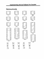
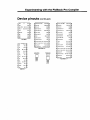
Appendix .
Component sources .
Device pinouts .
CDROM Contents .
Experimenting with the PicBasic Pro Compiler
Experimenting with the PicBasic Pro Compiler
Section-1
Display
Controller
Experiments
Simple serial LCD controller .
Multiple baud serial LCD controller .
Driving multiplexed 7-segment displays .
Substituting common Anode LED displays .
Interfacing to the MAX7219 LED display driver .
Experimenting with the PicBasic Pro Compiler
Program - SERLCD .BAS
Simple serial LCD controller
Intelligent LCD modules accept data and command instructions over a
four or eight bit parallel interface . Command instructions include : cursor
control, clearing, scrolling, etc . These commands are described in the
LCD module data sheet and in the compiler's manual . Thanks to the
LCDOUT command, these displays are not difficult to use, but still
require at least six precious pins from the PIC to be used . The serial LCD
controller described here, simplifies the use of these displays even more,
by enabling control of the LCD with a single wire . This is invaluable in
debugging your latest masterpiece, as it opens up a window into your
code . By connecting it to an unused pin and using the DEBUG command
at specific areas within the program, variables and registers can be
viewed .
The program SER_LCD .BAS implements a simple serial LCD controller
for use with the PIC16F84 .
When the PIC is powered up, the first thing It does is turn on the LCD
and wait the appropriate time for the display to be fully initialised, this
usually takes approximately 100ms . It then looks at the polarity switch,
and jumps to the appropriate section of code and displays : "T9600 Baud OK!"
or
"N9600 Baud OK!"
for true input
for inverted input
It then waits for a 9600-baud serial character of whichever polarity was
chosen . If the character is a special escape character (254), the next
character is assumed to be a command . The PIC will therefore pass the
following byte to the LCD as a command . Otherwise, the data will pass
directly to the LCD . This allows the display to be cleared scrolled, etc .
simply by sending data with an escape character in front of the control
byte: Serout PortB . 0, N9600,[254, 11
Pause 30
This will clear the LCD . Note the PAUSE command, this gives the LCD
module time to recover from the CLS command before sending another
character.
Section-1 - 1
Experimenting with the PicBasic Pro Compiler
Simple serial LCD controller
If a display with more or less than 2 lines is used then alter the last line of
the LCD defines : Define LCD_LINES
2
'Set number of lines on Display
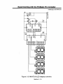
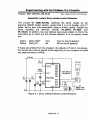
Figurel .1 shows the circuit of the Simple serial LCD controller. Serial
data enters through R5, this gives some protection to the PIC in the
event of a short circuit, it is also connected to one terminal of the DIL
switch (SW1) .
The DIL switch serves two purposes, first it configures the serial polarity
mode (inverted or true) by pulling PortB .4 to ground through R3, just
enough to register as a low reading (0), but not enough to interfere with
the output to the LCD . Sharing a pin like this is a common practice when
spare pins are not available .
Secondly, it stops the input from floating, (floating means that the pin is
neither set high or low) . This is achieved by resistors R2 and R4 . When
the polarity is configured for inverted mode, the left switch in the DIL
package is closed, which means that the right switch is open, thus
allowing only R4 to be connected to the input, this pulls the serial input
pin slightly towards ground . And when true polarity is selected, the left
switch in the DIL package is open and the right switch is closed, bringing
R2 into circuit, but as R2 has a lower resistance than R4 the serial input
pin is pulled more to the supply line . Without these resistors, random
characters would be displayed when the input was not connected to
anything.
78L05
9 Volts
IN OUT
0
GND
INTELLIGENT LCD
MODULE
Regulated 5 Volts
R11A91So5 1ai
RI
10k
RESET
MCLR
4nHo
Crystal
V
OSC1
PIC18F84
C3
ass22pfass 22pf
0502
R07
RBB
RB5
RB4
RB3
R82
RBI
RBO
R2
look
RA4
RA3
RA2
RA 1
VSS RAO
RS
1k
R4
220k
V
+5v
>
Seri 5I
Date
In
SWI
R3
7
Figures .1 . Simple serial LCD controller .
Section- 1 - 2
0
O
Experimenting with the PicBasic Pro Compiler
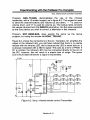
Programs - MULTILCD2.BAS & MULTILCD4.BAS
Multiple Baud Serial LCD controller
If, like me, you are fascinated by serial (RS232) communication, then this
project is a must . The baud rates are selectable from 300 to 19200 and
both inverted and non-inverted serial data is accepted . The circuit is, in
essence the same as the Simple controller, but with the exception of a
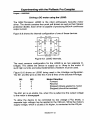
clever little switch called a Decimal Rotary DIL, figurel .2 shows the
pinout of one of these devices . It has ten rotary positions, numbered 0 to
9, and these numbers are represented as BCD
1 ,9 o y 8
outputs on pins, 1, 2, 4 and 8 .
C co
N c
4
1
.
C
9
V
2
The outputs of the switch are connected to RBO - RB4,
Figure 1 .2.
and by looking at these inputs, the program is able to
determine which baud rate is required i .e .
3 for 300 baud, 9 for 9600, 8 for 19200 (position 1 is already used) etc .
9
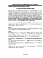
Figurel .3 shows the circuit for the multi-baud controller . Because of the
higher baud rates involved, a 16F873 running at 12mHz is used .
You may have noticed that the Vdd pin of the LCD is connected to
PortB .5 instead of the supply line, this is so that when the PIC is reset, all
ports are initialised as inputs by default, thus, also turning off the LCD,
and effectively resetting it . Therefore, the first thing the program does is
make PortB .5 an output, and turn the LCD on .
In order to read the rotary dil switch, the internal pullup resistors are
enabled on PortB, and the lower 4-bits are made inputs, we are only
interested in the pins that the switch is connected to, so the port is read
and the upper 4-bits are masked out by ANDing the result with
%00001111, the value held in B -TEST now holds the BCD output of the
switch . A lookup table is setup by using the LOOKUP command which
holds all the baud rates that will be selected (0-9), they have already
been divided by 100 (12 instead of 1200, 96 instead of 9600), this is
because the calculation to set the baud rate for SERIN2 is, (1000000 /
baud )- 20, however, this is too large a number for the compiler to
handle, therefore, it has to be scaled down, this is achieved by dividing
by 100 i .e . (10000/(baud/ 100)) - 20. After the LOOKUP command, the
variable BAUD holds the selected baud rate/100, then the above
calculation is carried out, and BAUD now holds the value to be placed in
the SERIN2 command .
Section- 1 - 3
Experimenting with the PicBasic Pro Compiler
Multiple baud serial LCD controller
To read the polarity switch, PortB .4 is made an input and bit-14 of BAUD
is set or cleared according to the result . Bit-14 is the mode setting, (1 =
inverted, 0 = non inverted) : TrisB.4=1
If P Test= 1 then
Baud. 14=0
Mode="T"
Else
Baud. 14=1
Mode="N"
Endif
TrisB.4=0
'Set PortB.4 to Input
'If P_ Test is high then Set for True Polarity
'Reset bit- 14 (Mode bit, clear for True)
'Variable used for the display
'Else Set for Inverted Polarity
'Set bit- 14 (Mode bit, set for Inverted)
'Variable used for the display
'Turn PortB.4 back to an output
The incoming serial data is then read in using the SERIN2 command, as
this can achieve higher baud rates than SERIN . The program now sits in
a loop, receiving data and outputting it to the LCD . If the control byte is
detected (254) the program is re-directed to a routine that input's another
serial character, this will be the byte that informs the LCD as to what
action should be taken, scroll, clear screen etc :Loop:
Serin2 SI,Baud,(RcvByte]
If RcvByte=254 then Control
Lcdout RcvByte
Goto Loop
Control:
Serin2 Sl,Baud,[RcvByte2]
If RcvByte2=253 then goto Bar
Lcdout RcvByte,Rcvbyte2
Goto Loop
'Receive the serial byte
' Trap the control byte
' Else display it on the LCD
' Keep on looking
'Receive the second serial byte
' Trap the Bargraph byte
'Or send out the two bytes
'Look again
Bar:
'Receive the Third and fourth serial byte
Serin2 SI,Baud,[Bar Pos,Bar_Val]
Lcdout
l,Bar Pos
'Position of bargraph
'Display the bargraph
Gosub Bargraph
Goto Loop
'Look again
Section-1 - 4
Experimenting with the PIcBasic Pro Compiler
Multiple baud serial LCD controller
INTELLIGENT LCD
MODULE
5 Volts
R1
10k
i
RESET
C2
1Ou1
Cl
0 .1u1
12mHz
Crystal
b~
s
ass ass
sa
VDD RC7 ie
17
RC6
8
RC5
e
RC4
MCLR
RC3
RC2
RC1
RCO
OSC1
PIC15F873
C3
15101
10
C4
151311
OSC2
VSSVSS
Y
RB7
RBA
RB5
RB4
RB3
RB2
RB1
RBO
0
0 0 0 0 o
S
w
3¢ >°
+SV
>
VR1
50k
e
5
R2
100k
a
i
RA5
RA4
RA3
RA2
RA1
RAO
x
e
SWI
0
e
SW2
R3
1k
0
Figurel .3 . Multi-baud serial controller .
Bargraph option
The Bargraph display is initiated by sending the control byte 253 along
with the position to start displaying from, and then the length of the bar : I
Bar
Line 1
Con 254
Con 253
Con 128
`Control Byte
`Bar display initiate
`Display line 1
3 .6 Volts
IIIIIIIIIIIIIIIIIIIIIIIIIIIIIIIIIIII
Debug l , Bar, Line 1, Length of_Bar : Pause 1
`Length of Bar' may be a value of 0 to 59 if a 4x20 display is used, or a
value of 0 to 47 for a 2x16 display . The PAUSE command allows the
serial controller time to do the bargraph subroutine .
The Bargraph subroutine is in the form of an include file, which is loaded
in after the LCD has initialised . The include file BARGRAF2 .INC is for
use with a 2x16 LCD, and BARGRAF4 .INC is for a 4x20 LCD. The code
is fully commented . The serial controller program MULTILCD2 .BAS is
for use with 2x16 LCD modules, and program MULTILCD4.BAS is for
use with 4x20 LCD modules . The program SER TEST.BAS
demonstrates the use of the bargraph option .
Section-1 - 5
Experimenting with the PicBasic Pro Compiler
Multiple baud serial LCD controller
Contrast control for an LCD module
If a contrast control is needed, it is simple enough to add a small preset
potentiometer connected to the Vo pin of the LCD, as in figurel .4.
Contrast increases as the pot is turned towards ground and the voltage
on Pin Vo decreases . Alternately, a fixed resistor with a value of a few
hundred ohms can be connected from Vo to ground.
INTELLIGENT LCD
MODULE
+5V
m
m ma a ma a°m 2W yjr o>>>
0 0
11111111111
VRII
50k
GND
Figurel .4 . LCD Contrast control .
Extended-temperature LCD modules on the other hand, require a
negative voltage applied to pin Vo, this can be achieved with a switchmode negative voltage converter, such as the MAXIM 1CL7660 . As
shown in figurel .5.
+5V IN
VDD
ICL7660
CAPC2
10uf
VOUT
CAP+
GND
Figurel .5. Switch-mode negative voltage generator .
Section-1 - 6
Experimenting with the PicBasic Pro Comp il er
Programs - 5CC_DISP.BAS
Driving multiplexed 7-segment LED displays
The main consideration when designing an interface to an LED display is
the number of pins available on the PIC . To drive a five digit nonmultiplexed display would require a PIC with 45 I/O pins, one for each
segment . This is of course impractical therefore, multiplexing is almost
universally adopted . Which will still take 13 pins, but on the larger PICs
with 33 I/Os this is not usually a problem .
As most of you will already know, multiplexing is accomplished by driving
each display in sequence . As each display is turned on, the segment
data from the PIC is set to the correct pattern for that digit . The patterns
for each digit are shown in table 1 .1 .
Binary value on A-G segments
F
E
C
B
1
1
1
1
1
1
1
0
0
0
0
1
1
0
1
1
1
1
0
0
1
0
0
1
1
1
1
0
1
0
1
1
1
1
0
0
1
1
0
1
1
1
1
1
1
0
0
1
1
Digit Displayed
0
1
2
3
4
5
6
7
8
9
0
0
1
1
1
1
1
0
1
1
A
1
0
1
1
0
1
0
1
1
1
Decimal
Table 1 .1 . Binary pattern for 7-segment digits .
63
6
91
79
102
109
124
7
127
103
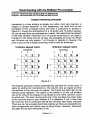
To illustrate how a single digit is displayed, we will look at digits 4 and 5 .
The binary pattern for digit 4 is %01100110, and for digit 5 it is
%01101101 . Figurel .6 shows how these binary patterns relate to the
segments to illuminate .
OFF 0
ON 1
ON,
OFF
OFF
ON
ON
0
0
1
1
•
••
A
D
0
A
7)
0
E
C
ON
OFF
ON
OFF
ON
ON
ON
1
0
1
0
1
1
1
A
0
G
es>•
e
IF
E
C
I
Figurel .6 . Binary relationship to illuminated segments .
Remember, that the 'A' segment is attached to the LSB of the binary
number .
Section-1 - 7
Experimenting with the PicBasic Pro Compiler
Driving multiplexed 7-segment displays
Connecting the display to the PIC is uncomplicated . The A-segment
connects to PortC bit-0, and the G-segment connects to PortC bit-6.
Segments B . .F connect to the pins in between . The decimal point is
connected to bit-7 of the same port .
In this demonstration, we shall be using common cathode displays . As
the name suggests, all the cathodes for the individual segment LEDs are
connected together internally, as shown below in figurel .7.
A
B
C
D
E
F
G
DP
Common
Figurel .7. Individual LEDs within a common cathode display .
By examining figurel .7 we can see that applying approx 2V to the anode
of a particular segment LED, while the common line is connected to
ground an individual segment may be illuminated .
To multiplex more than one display, requires us to take control of their
individual cathodes . This is achieved by a transistor acting as a switch,
as shown in figurel .8.
A
B
C
D
E
F
a
DP
Figurel .8 . Transistor switch .
A logic high on the base of the transistor will switch it on, thus pulling the
common cathodes to ground . R2 limits the current that can flow between
the individual segment LEDs . R1 limits the voltage supplied to the base
of the transistor.
We now have the means to switch each display on in turn, as well as the
information required to illuminate a specific digit . What's required now is
a means of turning on a display, illuminate the correct digit and do the
same thing for the next ones, quickly enough to fool the eye into thinking
it is seeing all the displays illuminated at once .
Section-1 - 8
Experimenting with the PicBasic Pro Compiler
Driving multiplexed 7-segment displays
And all within the background, to allow the program to process the actual
information to be displayed . This is a perfect application for a TMRO
interrupt using the compiler's ON INTERRUPT command .
Program 5CC_DISP .BAS shows a way of displaying a five-digit number
on five, 7-segment displays . Because the five displays require 13 I/O
pins, the program is intended to be used on one of the newer 16F87X
range of PICs, and also assumes a 20mHz oscillator is being used .
Figurel .10 shows the circuit layout for the demonstration .
The first thing the program does is initiate a TMRO interrupt (as shown in
the programming techniques section) to generate an interrupt every
1 .6384ms, by setting the prescaler to 1 :32 . To calculate the repetitive
rate of the interrupt use the following formula : Interrupt rate (in us) = ((OSC / 4) * 256) * prescaler ratio
Within the interrupt handler routine, the digit of interests pattern is
extracted by using the LOOKUP command, where a specific pattern
corresponds to a certain number held in the array NUM[O_C] . The
pattern extracted from the lookup table is placed into the variable
DISP PATT . The variable 0_C has a dual purpose ; its main purpose is
to form a sort of time-share for the individual displays . On each interrupt,
the variable O C is incremented, and each display waits for its particular
time-slot before it is turned on . This way each display is turned on for
approx 1 .6ms spread over five interrupts, causing an overall scan rate of
about 125Hz .
Within each display's time-slot, the previous display is turned off and the
value held in DISP PATT is placed onto PortC . A check is then made of
the variable DP which holds the decimal point placement . If DP holds the
value of the display we are currently using, the decimal point is turned on
by setting bit-7 of PortC . The display itself is then turned on by setting
the particular bit of PortB high . Note . DP may hold a value between 0 . .5
where 1 is the farthest right display, and zero disables the decimal point .
While the interrupt gives us a means of displaying five digits, the
subroutine DISPLAY does the processing of the actual number to
display . The subroutine first disables the interrupt to eliminate any
glitches that may be visible while processing the numbers, then it splits
Section-1 - 9
Experimenting with the PicBasic Pro Compiler
Programs -5,4,3,2CC_DISP.INC, MULT TST .BAS
Driving multiplexed 7-segment displays
the individual digits from the 16-bit number held in D_NUMBER using the
DIG operand . Each digit is placed into the five element array NUM, and a
series of if-then's zero suppress the unused digits . After all the digits
have been processed, the interrupt is re-enabled and the subroutine is
exited .
To aid in the use of multiplexing the displays, several include files have
been developed for use with 2 to 5 displays . The include file of choice
should be placed at the top of the program after the MODEDEFS .BAS
file has been included .
The include file 5CC_DISP.INC is for use when 5 displays are required
The TMRO interrupt will automatically be enabled upon the program's
start . It also contains the subroutine DISPLAY which expects two
variables to be pre-loaded before it is called . The first variable,
D -NUMBER holds the 16-bit value to be displayed . The second variable,
DP holds the position of the decimal point (0. .5) : D_NUMBER = 12345
DP= 0
Gosub Display
`Display the number 12345
'Do not place the decimal point
`Display the number
The include file 4CC_DISP.INC is for use when 4 displays are required .
Again, the TMRO interrupt is enabled on the program's start . The same
two variables need to be pre-loaded before the DISPLAY subroutine is
called . However, DP now has the range 0 . .4 .
The include files 3CC_DISP .INC and 2CC_DISP.INC are for use with 3
and 2 displays respectively.
The variables, D NUMBER and DP are already pre-declared within the
include file, therefore, there is no need to declare them in your program .
The program DISP TST.BAS demonstrates the use of 2 to 5 multiplexed
displays, by uncommenting the required include file . The program
increments a 16-bit variable, which is displayed on the 7-segment LEDs .
However, this loop could easily be replaced by the ADCIN command for
displaying the voltage converted . Or a temperature reading routine .
Section-l- 1 0
Experimenting with the PicBasic Pro Compiler
Programs -5,4,3,2CA_DISP .INC, MULT TST.BAS
Driving multiplexed 7-segment displays
Substituting Common Anode displays
If common anode displays are substituted for the common cathode types
then a slight re-arrangement of the switching transistors is required, as
shown in figurel .9 .
+5V
To PortB
Common
noao
B
C
D
To PortC
E
F
a
DP
A
-I
0
D
E
C
D
-DP,
Figurel .9 . Common Anode display .
A slight difference in the code is also required . The main difference is the
patterns that make up the digits . When common cathodes were used, a
high on the segments illuminated them, but for common anodes, a low
on the segments is required . Therefore, the patterns shown in table 1 .1
need to be inverted i .e . %11111100 becomes %00000011 . This can
easily be achieved by placing new values into the LOOKUP command
within the interrupt handler . The new patterns are shown below : [192,249,164,176,153,146,131,248,128,152,255]
One other thing that requires altering is the decimal point placement .
Previously PortC .7 was set high to turn on the point, but now it needs to
be pulled low . This again is easily remedied simply by changing the lines
corresponding to PortC .7 in the interrupt handler .
All the previous programs and include files discussed have already been
altered for use with common anode displays and may be found in the
COM ANOD folder.
Section-l- 1 1
Experimenting with the PicBasic Pro Compiler
Driving multiplexed 7-segment displays
Figurel .10 . 5-digit multiplexed common cathode display .
Section-l- 1 2
Experimenting with the PicBasic Pro Compiler
Driving multiplexed 7-segment displays
When using the multiplexer in your own program, you must remember
that it is using the compiler's ON INTERRUPT command . And as such
the precautions and work-arounds explained in the programming
techniques section should be observed .
If an oscillator of less than 20mHz is required, then the prescale value of
the interrupt should be decreased . Especially if more than four digits are
being utilized, otherwise a slight flickering of the display will be noticed .
This is easily accomplished by changing the three lines in the include
files that control the PSO, PS1, and PS2 bits of OPTION-REG . For
example, to use a 4mHz oscillator with a five digit display, the following
changes should be made : PSO = 0
PS 1 = 1
PS2 = 0
`Assign a 1 :8 prescaler to TMRO
By examining the include files for the different amount of multiplexed
displays, you will notice that as the amount of displays is reduced then
the interrupt rate is also decreased . The main reason for this is that, as
the interrupt handler is processing its multiplexing code, the main
program is halted until the interrupt is over, thus ultimately slowing it
down . The less times an interrupt handler needs to be called the quicker
the main program becomes .
A final note on multiplexing : When reducing the amount of displays used,
always remove the most significant digits . For example, if 4 displays are
used instead of 5 then remove display number 4, which is the leftmost
digit.
Section-l- 1 3
Experimenting with the PicBasic Pro Compiler
Program - MAX_CNT .BAS
Interfacing to the MAX7219
The MAX7219 is capable of driving up to eight common-cathode sevensegment LED displays using a three wire (synchronous serial interface) .
It can also convert binary-coded decimal (BCD) values into their
appropriate patterns of segments . And has built-in pulse-width
modulation and current-limiting circuits to control the brightness of the
displays with only a single external resistor .
With eight LED displays attached, the MAX7219 is able to scan them at
over 1200Hz, thus preventing any display flicker . If a display of less than
eight LEDs is used, the chip may be configured to scan only the one's
connected, increasing the brightness and scanning frequency of the
display. With all of its complexity one would expect the MAX7219 to be
difficult to control, but quite the opposite is true . With just a few lines of
code a versatile LED display can be realized and with only three pins
(data in, clock, and load) required on the PIC, even the 8-pin devices
may be used .
Connection to the LED displays is straightforward, pins SEG-A through
SEG-G and SEG DP-connect to segments A through G and the decimal
point of all of the common-cathode displays . Pins DIGIT-0 through
DIGIT-7 connect to the cathodes of each of the displays . Figurel .10
shows a typical setup using four LED displays, interfaced in this case
with a PIC16F84 .
Resistor R2 sets the current through each LED display . The smaller this
resistor is, the greater the current through each segment (minimum value
=9.53ko), a value of 10ko sets the current to 40mA per display . R3 is a
pulldown resistor on the interface between the PIC and the MAX7219
LOAD pin, this is required because when a PIC resets, its ports are
initialised as inputs . They are effectively disconnected, therefore,
anything connected to them is also disconnected, and are floating . Such
inputs frequently float high, however, electrical noise can cause them to
change states at random, this will normally cause the MAX7219 to go
into test mode with all segments lit . Therefore, R3 prevents this by
pulling the load pin more to ground when not in use .
Section-1- 1 4
Experimenting with the PicBasic Pro Compiler
Interfacing to the MAX7219
A
9
fO/
N
m
r
p
m
-AN
O0
$
O!
$
0
l°I°I-INI
O
xN
I>
0
4;V
7Zv
N
i
O
f0
00000000
i7 c~ i7 c~ c~ c~ G
O+N(JAUI6 J
0
O
mmmmmmmm
e
60000000
0 0000000
0 a
~ul e lulm
0 n
D
11
id
.
1910101 I I I
11
I'31 .
T
m
D
D
m o
11
Figure1 .10 . MAX7219 LED display controller.
Section-1- 1 5
Experimenting with the PicBasic Pro Compiler
Interfacing to the MAX7219
There are 14 addressable registers within the MAX7219, table 1 .1 shows
a list of them .
Register
NOP
Digit 0
Digit 1
Digit 2
Digit 3
Digit 4
Digit 5
Digit 6
Digit 7
Decode Mode
Intensity
Scan Limit
Shutdown
Test
Address
0
1
2
3
4
5
6
7
8
9
10
11
12
15
Description
No Operation
The first LED Display
The second LED Display
The third LED Display
The fourth LED Display
The fifth LED Display
The sixth LED Display
The seventh LED Display
The eighth LED Display
BCD decoding On/Off
Brightness of Displays
Amount of Displays attached
Place chip into Standby
Test mode On/Off
Table2 .1 . Registers within the MAX7219
Digit-0 - Digit-7 point to the relevant displays attached, digit-0 is the farright display .
Decode enables or disables BCD decoding for each individual display
(%1000000 1 would enable BCD on displays 0 and 7) .
Intensity sets the overall brightness of the displays (0 to 15) .
Scan Limit informs the MAX7219 as to how many displays are attached
(0-7) .
Shutdown, places the MAX7219 in standby mode when cleared .
Test, places the MAX7219 in test mode when set to 1 (maximum
brightness and all segments on) .
When sending data to the MAX7219 it expects a packet consisting of a
16-bit word containing the register number and then the value to be
placed within the register : First byte 11
Second byte 3
points to the scan limit register
informs the MAX that 4 LEDs are being used
The 16-bits are clocked into the MAX7219, regardless of the state on the
LOAD pin . However, they are only acted upon when the LOAD pin is
clocked high to low, which has the secondary effect of disabling the
device after the data is sent .
Section-l- 1 6
Experimenting with the PicBasic Pro Compiler
Interfacing to the MAX7219
Program MAX-CNT.BAS shows a simple application of the MAX7219 . In
the program, a 16-bit integer held in the variable COUNTER is
incremented and then decremented, this is displayed on the four 7segment LEDs . First the MAX7219 is initialised by loading the Scan
register with 3 (4 displays attached), the Luminance register with 3,
Decode register with %00001111, this will configure the first 4 displays to
BCD decoding, then the Switch register is set to one, which will wake up
the MAX7219 and finally the Test register is cleared .
The count up-down routine then places the position of the decimal point
in MAX _DP, (MAX DP may contain a value between 0 .. .7, zero being
the right-most display), and the value of COUNTER into MAX_DISP . The
subroutine DISPLAY is then called, this extracts the separate digits from
the variable MAX_DISP, using the DIG operand, and displays them on
the appropriate LEDs . Note the zero suppression, this is simply a series
of if then's that blank the digits by sending the value 15 when the display
is not being used . This subroutine itself calls another named
TRANSFER, which shifts out the two bytes then strobes the LOAD pin
low then high, this transfers the data into the internal registers of the
MAX7219 .
If more or less displays are used, change the value placed in
SCAN_REG (this is located in the initialisation section of code), to the
appropriate amount of LEDs attached (0-7) .
Also within the subroutine DISPLAY, change the lines :
into
For Position = 4 to 1 step -1
For Position = n to 1 step -1
Where n is the number of LEDs attached (1-8)
Into
If Digit >= 3 then Digit = 0
If Digit >= n then Digit = 0
Where n is the number of digits in the variable MAX_DISP (0-4), in
PicBasic Pro the maximum amount of digits is five (0 to 65535)
Section-l- 1 7
Experimenting with the PicBasic Pro Compiler
Section-2
Interfacing
with
Keypads
Keypad interfacing principals .
Interfacing with a 12-button keypad .
Interfacing with a 16-button keypad .
Serial keypad controller .
Receiving data from the keypad controller .
Assembler coded, keypad decoder .
Using the pseudo command, INKEYS .
Experimenting with the PicBasic Pro Compiler
Programs - KEYPAD12 .BAS, KEYTST12 .BAS and INKEYS12.INC
Programs - KEYPAD16 .BAS, KEYTST16.BAS and INKEYSI6.INC
Keypad interfacing principals
Interfacing to a few buttons is simple, but when more are required, a
keypad is almost essential . In this experiment, we shall look at the
principals of how a keypad works and write a subroutine to access it .
Figure 2 .1 shows the arrangement of a 12-button and 16-button keypad .
As can be seen they are arranged as a matrix, this minimizes the amount
of I/O lines needed, otherwise 12 or 16 inputs would have to be used to
interface to the same amount of keys . By arranging the keys into Rows
and Columns we only require 7 or 8 inputs to operate it, however, the
price to pay is that a keypad scanning routine must be employed .
12-Button keypad matrix
5
16-Button keypad matrix
Columns
6
7
5
Columns
7
6
8
Figure 2 .1 .
The keypad scanning routine systematically searches for a key press . It
starts by setting the connections to the column pins as inputs and the
connections to the row pins as outputs . The inputs are held high by the
internal pullup resistors. The object of the search is to find out whether
one of the rows of the keypad is connected to one of the columns, and if
so which one . The scan routine pulls one of the row lines low, then looks
at the columns input to see whether a 0 is detected . If not, it then tries
the next row ; this is continued until all the row lines have been scanned .
There are as many keypad scanning routines as there are programmers .
Each programmer has his/her way of doing things . However, whichever
way gets the job done effectively is OK.
Section-2 - 1
Experimenting with the PIcBasic Pro Compiler
Interfacing with a keypad
Interfacing with a 12-button keypad
The program KEYPAD12 .BAS, and the circuit shown in figure 2 .2
demonstrate the use of a 12-button keypad . The program scans the
keypad and displays the value of the key presses on a serial LCD
module connected to PortB .7 . It is based around the keypad scanning
subroutine INKEYS . When this subroutine is called, two variables are
returned . The first variable is KEY, which holds the value of the key
pressed (128 if no key pressed), the second variable returned is
DEBOUNCE, which (as you might have guessed) is a debounce flag .
This returns holding a zero if a key has been pressed, however, when
the INKEYS subroutine is called a second time and a key is still in use, a
value of one is returned . One possible use of this feature could be : Main:
Gosub Inkeys
if Debounce= 1 then goto Main
'Go scan the keypad
'Go back if button is still held
Within the INKEYS subroutine the variable DEBOUNCE is initially set to
1, then the first four bits of PortA are configured as outputs (rows), and
the first three bits of PortB are setup as inputs (columns) . Care has been
taken to configure only the relevant bits that the keypad is attached to .
The internal weak pullup resistors are enabled and the first row is pulled
low (PortA .3), the subroutine SCANCOL is then called, this examines the
column lines in turn and increments the variable KEY when a keypress
has not been detected, this will build up 13 numbers corresponding the a
certain keypress or no keypress (albeit in the wrong order) . On returning,
the variable K_ FLAG will hold 1 if a keypress was detected otherwise it
holds 0 . The variable K_FLAG is examined after its return, to ascertain
whether to scan the next row or to process the value held in KEY . If
K FLAG returned 0, then the same procedure is carried out for all four
rows . However, if K FLAG returned a 1 then the debounce flags are set
or cleared accordingly to the value held in D -FLAG . The variable KEY is
re-arranged to correspond to the keypad legends, by using the LOOKUP
command : Map of the keypad legends for numeric output
Lookup Key,[1,2,3,4,5,6,7,8,9,10,0,11,128J,Key
Section-2 - 2
Experimenting with the PicBasic Pro Compiler
Interfacing with a keypad
For example, in its raw state, KEY will hold the value 0 if the one key has
been pressed, 10 if the zero key has been pressed, and 12 if no
keypress has been detected, therefore, the thirteen values within the
braces of the LOOKUP command correspond to the raw KEY values and
the expected keypad legend values .
The program KEYTST12 .BAS does the same as KEYPAD12 .BAS, but
the INKEYS subroutine is loaded in as an include file : Include "INKEYS12.INC"
`Place this at the beginning of the program .
To
Serial LCD
N9600 baud
5 Volts
VDD RB7
MCLR RB6
RB5
RB4
RB3
0SC1 RB2
RB1
RBO
PIC16F84
RA4
OSC2 RA3
RA2
RA1
RAO
vss
Figure 2 .2 . 12-button Keypad Circuit .
Section-2 - 3
Experimenting with the PicBasic Pro Compiler
Interfacing with a keypad
Interfacing with a 16-button keypad
Using a 16-button keypad is essentially the same as using the 12-button
version, however, minor differences in the INKEYS subroutine have to
be made . Figure 2 .3 shows the slightly different circuit layout and
program KEYPAD16 .BAS demonstrates its use . The keypad is again
arranged as a matrix, but this time it is 4x4, (four columns and four rows) .
Within the INKEYS subroutine most of the code stays the same, it still
scans the four rows, but this time there are four columns instead of three .
Therefore, one extra input is required which means the TRIS value has
to take this into account . As with the 12-button program, the value
returned in KEY from the subroutine SCANCOL does not match up with
the legends printed on the keypad's buttons . Therefore, the LOOKUP
command is used again to change the value returned in KEY to the
correct number. However, this time there are 17 different combinations .
'Map of the keypad legends for numeric output
Lookup Key,[15,7,4,1,0,8,5,2,14,9,6,3,13,12,11,10,128],Key
The program KEYTST16 .BAS does the same as KEYPAD16.BAS, but
the INKEYS subroutine is loaded in as an include file : Include "INKEYS16.INC"
'Place this at the beginning of the program .
To
Serial LCD
N9600 baud
5 Volts
R1
4.7k
VDD
MCLR
4mHz
Crystal
1
C1
L' 10uf
C2 ses
Slut
Dv
I
C3
M 22p1
OSC1
16
C4
22pt
PIC18F84
OSC2
VSS
RB7
RB6
RB5
RB4
RB3
RB2
RB1
R BO
a
B
RA4
RA3
RA2
RA1
RAO
I
Figure 2 .3 . 16-button Keypad Circuit .
Section-2 - 4
Experimenting with the PicBasic Pro Compiler
Interfacing with a keypad
In both the 12 and 16 button demonstration programs, the value returned
in the variable KEY is a numeric representation of the key pressed (i.e .
key one returns the value 1) . However, if the ACSII representation is
desired (i.e . key one returns the value 49), the commented LOOKUP
command needs to be uncommented and the initial LOOKUP command
needs to be commented .
'Map of the 12-button keypad legends for ASCII output
"0", 11#11, 321, Key
Lookup Key, j"11 , 2", 11311,"4", 115" 11611,"7", "8",
'Map of the 16-button keypad legends for ASCII output
„En 11911,116"1"3", „p„ „C , .8,. A''
Lookup Key,["F' "71,114 ",'l „ "0"„8„ '5","2",
Key
If your particular keypad does not match up with the values displayed,
simply re-arrange the values within the braces of the LOOKUP
command .
To determine which keys are which, comment the LOOKUP command
and place a SEROUT or DEBUG command just after it . This will display
the value held in the variable KEY . Whichever value is returned for the 0
button will be the first value within the braces of the LOOKUP command .
Section- 2 - 5
Experimenting with the PicBasic Pro Compiler
Program - SERKEY .BAS
Serial keypad controller
The use of a keypad is often essential but it still takes up precious pins
on the microcontroller that could have other functions, therefore, the
logical solution is to send out the data from the keypad serially . This
means that only one or two pins are used up on the PIC . Figure 2 .4
shows the circuit for such a controller . The keypad controller sends out
async serial data at either T1200 baud or T9600 baud .
The three LINKS connected to PortA and PortB ; configure several
different properties within the controller code .
LINK1 configures the serial output baud rate . When connected, 9600 is
transmitted, and when left unconnected, 1200 baud is transmitted . The
lower baud has been chosen so that a serial IR transmitter or a radio
transmitter may be connected .
LINK2 selects the output type . When connected, ASCII values are
transmitted, where the value sent reflects the ASCII value of the key
(button A will send the value 65) . When unconnected, numeric values
are transmitted, where the actual key values are sent (button 3 will send
the value 3) .
LINK3 selects the number of buttons on the particular keypad used .
Connected will interface to a 16-button keypad, and unconnected will
interface with a 12-button type .
The STROBE pin (PortB .6), will be high 50ms before the serial data is
transmitted, and low just after the end of transmission . This may be
used as an indicator or as a data validation line to the receiving PIC that
a key has been pressed and serial data is on its way . By using the NAP
command within the waiting loop of the main program, the controllers
current consumption is only 0 .4mA .
Section-2 - 6
Experimenting with the PicBasic Pro Compiler
Serial keypad controller
The program, SERKEY.BAS is based around the keypad scanning
subroutine INKEYS, this is a modified version of the standard
subroutines explained in the previous experiments . The main loop of the
program examines the pins where the links are attached, and places
their value into three flags, BUTTONS, NUMERIC, and BAUDRATE,
these now contain 1 or 0 according to whether the pins are connected or
not. The internal pullups and R2 ensure that when a link is not connected
the pin will always remain high .
The linkk flags are used to construct the different configurations by simple
if-then commands located at places within the code that require a
different product for the specified link connection or disconnection .
The format for the serial data transmitted is : Sync byte "l7 ", Key Value, Debounce flag
This is sent as True polarity 9600 or 1200 baud .
Low current consumption is achieved by continuously using the NAP
command when no key is pressed . This means that the PIC is off more
than it is on . The NAP command places the PIC into low power mode for
18ms, which means there is an 18ms delay before the keypress is
responded to, however, this is not noticed as the keypad is not a time
critical component .
Again :
Gosub Inkeys
'Go and scan the keypad
If Key= 128 or Key=32 then 'If no key pressed do the following : 'Go into low power mode for 18ms
Nap 0
'And look again when woken up .
Goto Again
Endif
The circuit shows a 16-button keypad connected, however, if a 12-button
type is used instead, connections are as figure 2 .2.
Section-2 - 7
d
L
E
0
U
+5 Volts
0
Link 1
Connected . . .9600 baud
Open
1200 baud
R1
4 .7k
a
V
MCLR
aa)
4mHz
Crystal
L
a+
.C
0)
C
P1C16F84
b C1
00 10uf
C2
C
a)
E
a)
y
a
W
OSC1
V-
"
0 u"
C3
- r22pf
TT T
4
C4
22pf
RB7
RB6
RB5
RB4
RB3
RB2
RB1
RBO
C:
0
U
a
a)
Q
a
Y
a)
u)
RA4
OSC2
RA3
RA2
RA1
VSS RAO
s
Link 3
Connected . . .16-button keypad
Open
12-button keypad
0
14
VDD
as
3
Link 2
Connected . . .ASCII output
Open
Numeric output
N
a))
0)
J J J
LL
Experimenting with the PicBasic Pro Compiler
Program - KEYIN .BAS
Receiving data from the serial keypad controller
The program KEYIN.BAS demonstrates how to receive the serial data
from the serial keypad controller and display the results on a serial LCD
display, connected to PortA .1, configured for N9600 baud . The
subroutine KEVIN continually looks for the sync byte "@" and when
found, reads in the next two bytes which contain the value of the key
pressed, and the debounce flag . It then returns with these values in the
variables KEY and DEBOUNCE : Byte
`Button pressed variable
Key
Var
'Debounce Flag
Debounce Var
Byte
Keyin :
`Look for the sync byte
Serin PortA .0,T9600,Key
`Look again if not found
If Key<>"@ " then goto Keyin
Serin PortA . 0, T9600, Key, Debounce
Return
Alternatively, the SERIN2 or DEBUGIN commands may be used . These
have the ability to wait for a specific sequence of characters before
receiving the Key and Debounce data, and not surprisingly, this operand
is called WAIT . The subroutine above can be changed to : Byte
`Button pressed variable
Key
Var
'Debounce Flag
Debounce Var
Byte
Con 84
79600 baud
B9600
Keyin :
Serin2 PortA . 0, B9600, [ wait ("@") , Key, Debounce]
Return
Timeout values may be added, so that if a key is not pressed within a
certain time frame the subroutine is exited . The flexibility of the
compiler's serial data commands are too numerous to explain, the PBP
manual should never be far away .
Alternatively the STROBE pin may be connected and periodically
examined, if it is high then the keypad is transmitting, and low means the
keypad is untouched .
Section-2 - 9
Experimenting with the PIcBasic Pro Compiler
Programs - ASM_KEY .BAS & ASM KEY.INC
Assembler coded, Keypad decoder
The assembler coded, keypad decoder is in the form of an include file
ASM KEY .INC, its use is essentially the same as the BASIC coded
versions, except there is no debounce flag returned i .e. DEBOUNCE .
There are however, two new Defines added for the keypad, the first,
informs the subroutine whether a 12 or 16-button keypad is being used,
these are: or
Define
KEYPAD_ BUTTONS 12
`Use a 12-button keypad
Define
KEYPAD BUTTONS 16
`Use a 16-button keypad
The wiring of the keypads are*shown in figures 4 .2 and 4 .3.
The second Define informs the subroutine, whether to return the variable
KEY with the ASCII value of the key pressed or the numeric value : or
Define
KEYPAD RETURN
0
`Return the numeric value
Define
KEYPAD RETURN
1
`Return the ASCII value
If the NUMERIC value is chosen, the variable, KEY will be returned from
the subroutine holding the numeric equivalent of the legends printed on
the keypad buttons (0 will return a value of 0, A will return a value of 10
etc.), and 128 if no button pressed . If the ASCII value is chosen, KEY will
return holding the ASCII equivalent of the legends printed on the keypad
buttons (0 will return a value of 48, A will return a value of 65 etc.), and
32 (space) if no button pressed .
If no Defines are added to your program, the default settings are, 12button keypad, returning the NUMERIC values .
The ports on which the keypad is connected, are automatically
configured for the correct input/output configuration each time a call is
made to the subroutine INKEYS . And the variable, KEY is already predeclared within the include file . Make sure that the include file is placed
at the beginning of your program, in order to minimize the risk of page
boundary conflicts . The program ASM_KEY.BAS is a demonstration for
using the assembler coded keypad decoder .
Section-2- 1 0
Experimenting with the PicBasic Pro Compiler
INKEYS, pseudo command
Within the include files INKEYS12 .INC and INKEYS16 .INC, a macro has
been defined which allows the use of a pseudo command called
INKEYS . Instead of calling the subroutine INKEYS and having the value
of the key pressed returned in KEY, and the debounce flag in
DEBOUNCE, we can place these values into any variable we choose .
The use of the INKEYS command is : Variablel
Variable2
@
Var
Var
Byte BANKO
Byte BANKO
SYSTEM
SYSTEM
INKEYS Variablel, Variable2
Variable 1 will hold the key pressed and Variable2 will hold the debounce
flag . There are three things to remember when using the pseudo
command . Always place the @ symbol at the beginning of the line, also
any variables used within the command should be declared as BANKO
variables .
Also, don't forget to declare the variables as SYSTEM types, or an
underscore must precede them .
Both variables are optional, if Variable2 is not used the debounce flag
will be placed into DEBOUNCE . And if Variablel is not used the key
value will be placed into KEY .
Section-2 - 1 1
Experimenting with the PicBasic Pro Compiler
Section-3
Experimenting
with
Serial Eeproms
Giving the PIC a memory .
Microwire Interface principals .
SPI Interface principals .
12C Interface principals .
12C eeprom interfacing principals
Interfacing to the 24C32, 1 2C serial eeprom .
Interfacing to the 24C32 using the MSSP module .
Interfacing to the 93C66, Microwire serial eeprom .
Interfacing to the 25LC640, SPI serial eeprom .
Experimenting with the PicBasic Pro Compiler
Giving the PIC a memory.
If you have a project that requires long-term memory storage (up to 200
that will not fit into the PIC's internal eeprom, an external serial
eeprom (SEEPROM) may be the answer . These small and inexpensive
devices are easily interfaced to any of the PIC range . This section is a
guide to choosing and using seeproms . We will compare the three major
interface types : Microwire, SPI, and 1 2C, also the advantages and
disadvantages of using each type .
years)
All serial eeproms use a synchronous serial interface (SSI), this means
that both the eeprom and the microcontroller use a common clock and a
clock transition signal to indicate when to send or read each bit . Some
synchronous serial devices require minimum clock frequencies, the clock
for seeproms can be as slow as required, or as fast as a few mHz's . The
microcontroller can strobe the clock at its convenience, up to the
maximum speed of the device .
Serial eeproms normally have just eight pins, power, ground, one or two
data/address lines, and a clock input, plus up to three other control
signals . However, unlike parallel eeproms, which require extra pins to be
added as the number of address and data lines grow, a seeprom's
physical size does not have to increase with its memory capacity .
Eeproms use CMOS technology ; therefore, they consume minute
amounts of power, with currents as low as a few uA in standby mode and
a mA or so when active .
Depending on the device, the maximum clock speed for accessing serial
eeproms may be over 2mHz. However, because it takes eight clock
cycles to transfer a byte, and the master also needs to send instructions
and addresses, the maximum rate of data transfer is usually no more
than 4ms per byte . Write operations actually take much longer, because
the eeprom needs several milliseconds to program a byte into its
memory array. During this time, the PIC cannot read or write to the
eeprom .
With continued use, eeproms eventually lose their ability to store data, so
they are not suited for applications where the data changes constantly .
Section-3 - 1
Experimenting with the PicBasic Pro Compiler
Giving the PIC a memory
Most are rated for between 1 million and 10 million erase/writes, which is
OK for data that changes occasionally, or even every few minutes .
It's not only eeproms that use a serial interface, other devices with
synchronous serial interfaces include, AID, D/A converters, clocks, and
display interfaces etc, all of these devices are used extensively in this
book . Therefore, this section will give an insight on how other devices
using a serial interface communicate with the PIC . Multiple devices can
connect to one set of data lines, with each chip having its own ChipSelect line (CS) or firmware address, this effectively means that if two
devices are connected then the second device may only require one
extra pin .
After you have decided to use a serial eeprom, the next step is to select
one of the three serial protocols . In conventional assembler
programming, the 3-wire devices won easily because of the simplicity of
their interface . However, with the compiler's 1 2C and Shift commands,
interfacing to any of the devices is greatly simplified .
To see how the different interfaces compare, we will look at an eeprom
of each type .
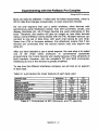
Table 3 .1 summarizes the major features of each type used .
Interface Type
Device
Memory capacity
Number of Interface pins
Date width (bits)
Maximum clock speed
Write (busy) time
Max No. of bytes programmed In one operation
Writes bit on (clock state)
Reads bit on (clock state)
Chip select method
Microwire
93C66
4Kbits
4 or 3
8 or 16
2mHz
10ms
2
Rising edge
Rising edge
Hardware
SPI
25LC640
64Kbits
4 or 3
8
2mHz
5ms
32
Rising edge
Failing edge
Hardware
I`C
24C32
32Kbits
2
8 or 16
400kHz
10ms
16
Low level
Low level
Software
Table 3 .1 . Comparison of SPI, Microwire, and I C eeproms .
Section-3 - 2
Experimenting with the PicBasic Pro Compiler
Giving the PIC a memory
Microwire interface principals
Atmel's 93C66 is an 8-pin, 4Kbit serial eeprom with a Microwire
interface . It has two data pins, data in (DJ) and data out (DO), a clock
input (SK), and a chip-select (CS) . Additional inputs are for memory
configuration, (ORG), which determines whether data format is 8 or 16bits, and program enable (PE), which must be high to program the chip .
The memory is organised as 256 words of 16-bits each when the ORG
pin is attached to Vcc, and 512 words of 8-bits each when ORG is
connected to ground .
Although it is sometimes called a 3-wire interface, a complete connection
actually requires four signal lines . However, use of the PIC's ability to
rapidly switch states from input to output means that the data in and data
out pins may be connected to the same pin on the PIC .
The eeprom understands seven instructions, these are, ERASE/WRITE
ENABLE and DISABLE, WRITE, READ, ERASE, ERASE ALL (sets all
bits to 1), and WRITE ALL (writes one byte value to all locations) . Each
instruction must begin with a Start condition, which occurs when CS and
DI are both high on the clocks rising edge . DI is brought high naturally
when an instruction is written, because all of the instructions begin with
one . The PIC must bring CS low after each instruction, except for a
sequential read . When CS is brought high, the eeprom is placed into
standby, ignoring all instructions until it detects a new start condition .
To write to the eeprom, the PIC must first send an ERASE/WRITE
ENABLE instruction to DI, followed by a WRITE instruction, the write bits
are written on the clocks falling edge, and the eeprom latches each bit on
the next rising edge . After sending the final data bit in a programming
sequence, the PIC must bring CS low before the next rising edge of the
clock (SK) . This causes the eeprom to begin its internal programming
cycle . The programming is self-timed which means that it requires no
clock cycles . If CS returns high before the programming cycle is
complete, DO will indicate Ready/Busy status . CS must then go low
again to complete the write operation .
The PIC needs to send the Erase/Write Enable instruction just once per
programming session . The device remains write-enabled until it receives
an Erase/Write Disable instruction or power is removed .
Section-3 - 3
Experimenting with the PicBasic Pro Compiler
Giving the PIC a memory
To read from the eeprom, the PIC sends a READ instruction to DI,
followed by the address to read . When the eeprom receives the final
address bit, it writes a dummy zero to DO, then writes the requested data
on the clocks rising edges .
If CS remains high after a read operation, additional clock transitions will
cause the chip to continue to output data at sequential addresses . If CS
goes low, the next read operation must begin with the read instruction
and an address .
SPI Interface principals
SPI is very similar to Microwire, although polarities and other details
vary. As with Microwire, SPI eeproms write bits on the clock's rising
edge, however, unlike Microwire, they latch input bits on the falling edge .
The polarity of CS (active low) is also opposite from the Microwire
convention
Microchip's 25LC640 is a 64Kbit eeprom with an SPI interface, organised
as 8192 words x 8-bits . In addition to the four interface lines, the chip has
two other inputs . WP (write protect), which must be high to program the
device . Moreover, for interfaces with multiple slaves, the HOLD input
enables the PIC to pause in the middle of a transfer in order to do
something more urgent on the SPI bus. The eeprom ignores all activity
on the SPI bus until HOLD returns high, then both devices carry on
where they left off .
The eeprom understands six instructions, these are, SET AND RESET
THE WRITE ENABLE LATCH, READ AND WRITE TO THE STATUS
REGISTER, and READ AND WRITE TO THE MEMORY ARRAY . The
eeprom has several levels of write protection, which may be used to
virtually guarantee that there will be no unintentional writes to the device .
If WP is low, no changes to the data are allowed . If WP is high, two nonvolatile bits in the chip's status register can block writes to all, or a
portion of the device . Finally, if WP is high, before you can write to the
status register or the portion of memory enabled in the status register,
the eeprom must receive a Set Write Enable Latch instruction .
Section-3 - 4
Experimenting with the PicBasic Pro Compiler
Giving the PIC a memory
To write to the eeprom, the PIC sends a SET WRITE ENABLE LATCH
instruction to SI, followed by a WRITE instruction, then the highbyte and
lowbyte of the address are sent, then the data to write . The PIC may
send up to four data bytes for sequential addresses in one operation .
After clocking the final data bit with SCK low, CS must go high to begin
programming the byte into the eeprom .
While the eeprom is programming the data, the PIC can read the
eeprom's status register . When bit-0 of the status register is 0, the
eeprom has finished programming, and the next write operation may
begin . The chip is write-protected after each programming operation ;
therefore, each write must begin with a SET WRITE ENABLE LATCH
instruction .
To read the eeprom, the PIC sends a READ instruction followed by the
highbyte and the lowbyte of the address . The eeprom responds with the
data bits in sequence on SO . As with Microwire, additional clocks will
cause the eeprom to send additional data bytes in sequence .
Section-3 - 5
Experimenting with the PicBasic Pro Compiler
Giving the PIC a memory
12C Interface principals
1 2C is a synchronous serial bus, developed by Philips to allow
communication between different peripherals . Many devices such as
eeproms, ADCs, LCD drivers, DACs, etc support the 1 2 C bus protocol .
These devices communicate through a 2-wire bus, with data transfer
rates of 100Kbit/s, 400Kbit/s, and even 1 Mbit/s . The number of devices
on the bus is limited by the maximum bus capacitance of 400pF .
Most devices are used as slaves while microcontrollers are typically
masters . 1 2C also supports multi-mastering, which means more than one
device is allowed to control the bus . 12C has collision detection and
arbitration to maintain data integrity . The two lines used for 1 2 C
interfacing are, Serial Data Address Line (SDA) and Serial Clock Line
(SCL) . Both of these are bi-directional .
1 2 C : Protocol
1 2 C is a multi-master/slave protocol . All devices connected to the bus
must have an open-collector or open-drain output . A transaction begins
when the bus is free (i.e. both SCL and SDA are high), a master may
initiate a transfer by generating a START condition . Then the master
sends an address byte that contains the slave address and transfer
direction . The addressed slave device must then acknowledge the
master . If the transfer direction is from master to slave, the master
becomes the transmitter and writes to the bus . While the slave becomes
the receiver and reads the data and acknowledges the transmitter, and
vice-versa . When the transfer is complete, the master sends a STOP
condition and the bus becomes free . In both transfer directions ; the
master generates the clock SCL and the START/STOP conditions .
i-saSCL
e a
setup
time
SDA
(start condition)
.(up
~ rme
SDA
(stop condition)
h oi
i
a
Figure 3 .1 . 1 2C START/STOP conditions .
Section- 3 - 6
Experimenting with the PicBasic Pro Compiler
Giving the PIC a memory
The START condition is generated by a high to low transition on the SDA
line during the High period of the SCL line, as shown in figure 3 .1 .
A stop condition is generated by a low to high transition on the SDA line
during the High period of the SCL line, also shown in figure 3 .1 .
The number of bytes transferred per START/STOP frame is unrestricted .
Data bytes must be 8-bits long with the most significant bit (MSB) first.
Each valid data bit sent to the SDA line must remain high for '1' or low for
'0' during the high period of the SCL, otherwise any transition in the SDA
line while SCL is high will be read as a START/STOP condition . Thus,
transitions can only be made during the low period of SCL . An
acknowledge bit must follow each byte . After the last bit of the byte is
sent, an ACK clock (acknowledgement clock) is generated by the master
(9t`' clock) . An ACK (acknowledge bit, low) must be sent by the receiver
and remain low during the high period of the ACK clock .
If the slave (receiver) doesn't return an ACK (e.g. an error, or is unable to
receive the data), then the slave device must leave the SDA line high
(NACK). The master will abort the transfer by generating a STOP
condition . If the slave does return an ACK, but sometime later it is unable
to receive any more data . Then the slave must generate a NACK (not
acknowledge, high) on the first byte to follow . The slave will then need to
keep the SDA line high for the master to generate a stop condition . If the
receiver is the master and the transfer is ending . Then the master needs
to send a NACK after the last byte is sent . The slave (now a transmitter)
must release the SDA line to high, this allow the master to generate a
START/STOP condition .
At the beginning of each transfer, the master generates the START
condition then sends a slave address . The standard slave address is 7bits (sometimes 10-bits) followed by a direction or R/W bit (8"t bit) as
shown in figures 4 .2 and 4.3 . When the direction bit is a WRITE (zero),
the addressed slave device becomes the receiver and the master
becomes the transmitter. When the direction bit is a READ (one), the
addressed slave device becomes the transmitter and the master
becomes the receiver .
Section-3 - 7
Experimenting with the PicBasic Pro Compiler
Giving the PIC a memory
12C Serial eeprom interface principals
Microchip's 24C32 is a 32Kbit serial eeprom using an 1 2C interface, the
memory organisation is 4096 words x 8-bits, or 2048 words x 16-bits .
The slave address assigned to this device by the manufacturer is
101OXXX, where X = Don't Care . The eeprom supports several transfer
modes such as, BYTE WRITE, PAGE WRITE, CURRENT ADDRESS
READ, RANDOM READ, and SEQUENTIAL READ .
To perform a Byte Write, the master generates a START condition and
sends the slave address with the direction bit set to WRITE (zero) as in
figure 3 .2 . When the slave device matches the address, it sends an ACK
to the master during the ninth clock cycle . The next byte sent to the
eeprom will be the word address that moves its internal address pointer .
Then the data sent by the master will be written to the memory location
pointed to by this address . Finally, the master generates a STOP
condition, which will signal the eeprom to initiate the internal write cycle .
At this time the eeprom will not generate any acknowledge signals until
the transaction is complete .
A Page Write is similar to a Byte Write, except the master may transmit
up to eight bytes before generating a stop condition . Each byte sent to
the device will increment the address pointer for the next byte
transaction . The eeprom stores the data in an eight-byte buffer, which is
then written to memory after the device has received a stop condition
from the master, as in figure 3 .2.
Control Byte
Word Address
Byte Write
_- i,oi
I
IA
Byte
I 0 I I 0 I X IX
1
W
d Address (n]I A` Date (n)
Page Write
S : START condition
W : Write bit (low)
A : ACK bit
P: STOP condition
R : Read bit (high)
N : NACK bit
El
I A (Data (n+11 A I
From Master to Slave
From Slave to Master
Figure 3 .2 . Write transfers .
Section-3 - 8
D t (n+7
A
IPi
Experimenting with the PicBasic Pro Compiler
Giving the PIC a memory
Read operations are initiated the same way as a write operation except
the direction bit is set to READ (one) . The eeprom keeps the address
pointer from the last byte accessed incremented by one . In a Current
Address Read transaction, the eeprom acknowledges the master after
receiving the slave address and transmits the data byte pointed by its
internal address pointer, see figure 3 .3 . The pointer is incremented by
one for the next transaction . Sequential Reads behave the same way as
a Current Address Read transaction except data is continually
transmitted by the slave device until the master generates a STOP
condition see figure 3.3 .
For Random Read, the master generates a START condition then sends
the slave address with the direction bit set to WRITE (zero) . Then the
next byte sent is the word address to be accessed . This operation will
change the eeprom's internal address pointer . Then without generating a
STOP condition, a Current Address Read or Sequential Read transaction
will follow .
Notice that the Current Address Read and Sequential Read transaction
generate another START condition, as shown in figure 3 .3 .
0
C
®
©UUBU
Data
d
an
Word Address In) I A
A I Data [n] I°N; P-J
Random Read
~
bo0
arls
~
Data In]
J,A jData [n+1]lkr
Data [n+2] A
Sequential Read
S : START condition P : STOP condition
R: Read bit (high)
W : Write bit (low)
A : ACK bit
N: NACK bit
I
Data (n
]
Do
From Master to Slave
D
From Slave to Master
Figure P .3 . Read transfers .
Section- 3 - 9
Experimenting with the PicBasic Pro Compiler
Programs - 24C32 .BAS, 24X_TST .BAS and 24XXX .INC
Interfacing to the 24C32 eeprom
Interfacing to the 24C321 2C eeprom
Now that we know the principals behind serial eeprom interfacing, we
can develop a pair of subroutines that will automate reading and writing
to them . The Microchip 24C32 is an 1 2C device that can store 4096 bytes
of data. Figure 3 .4 shows the eeproms connections to the PIC .
+5 Volts
VCc
WP
SSA
SCL
24C32
AO
A1
A2
i
v
Figure 3 .4. 24C32 eeprom connections.
Writing to the eeprom
The subroutine EWRITE is used for this purpose . It expects two
variables to be pre-loaded before its use . The first is the address within
the eeprom where the data is to be stored, this is held in the 16-bit
variable ADDR, the second is the data to write to the eeprom, this is held
in the variable E BYTEOUT .
Within the EWRITE subroutine, the I2CWRITE command sends three
lots of data to the 12C bus ; firstly the slave address is sent, (this must
always start with % 1010, which is the serial eeprom device identifier) . If
there is more than one eeprom on the 1 2C bus then the next three bits will
reflect the pattern on the A2, Al and AO pins . However, for this
demonstration we are only using one device, therefore, they are cleared .
So the slave address is %10100000, the I2CWRITE command will
automatically set the read/write bit . The next lot of data sent is the 16-bit
memory address, and finally the BYTE or WORD sized value to be
placed at the address location is sent . A delay of 10ms is required after
the write is performed ; this allows the eeprom time to allocate the data
into its memory array : EWrite:
12CWRITE SDA,SCL, % 10100000,Addr,[E_ByteOut] 'Write the byte
Pause 10
'Delay 10ms after each write
Return
Section-3 - 1 0
Experimenting with the PicBasic Pro Compiler
Interfacing to the 24C32 eeprom
If the variable E_BYTEOUT is declared as a BYTE, then 8-bits will be
written . If the variable is declared as a WORD then 16-bits will be written
Reading from the eeprom
The subroutine EREAD is used for this purpose . It reads 8 or 16-bits
from the eeprom . Before the subroutine is called, the address of interest
must be loaded into the variable ADDR . Upon returning from the
subroutine, the data from the specified address location is held in the
variable E BYTEIN.
The EREAD subroutine uses the I2CREAD command . The slave
address (as in EWRITE) and the 16-bit memory address are sent . Then
the data is read into the assigned variable . Its use is: `Point to location 1024 within the eeprom
ADDR = 1024
'Read the data from the specified location
Gosub Eread
The variable E_BYTEIN now holds the byte of data
ERead:
12CREAD SDA, SCL, % 10100000,Addr, jE BytelnJ 'Read the byte
Return
Unfortunately, the compiler's 12CREAD and I2CWRITE commands do
not use the acknowledge returns from the bus . Therefore, this method
cannot be used to verify whether a successful write has been performed .
One way to get round this, is to read the data back from the same
address that it has just been written to, and compare the result .
For example .
Write:
` Point to location 1024 within the eeprom
ADDR = 1024
'Place the value 128 in the address
E BYTEOUT = 128
` Write the byte to the specified address
Gosub EWrite
`Read the data from the same address
Gosub Eread
`Compare them
If E Bytein <> E Byteout then goto WRITE
This compares the variable E_BYTEIN with the variable E BYTEOUT,
and if they are not the same then the WRITE process is carried out
again . This will slow down the writing process slightly, but a successful
write is guaranteed . Unless the eeprom has come to the end of its life .
Section-3 - 1 1
Experimenting with the PicBasic Pro Compiler
Interfacing to the 24C32 eeprom
The include file 24XXX .INC, contains the two subroutines, EREAD, and
EWRITE . This should be loaded near the beginning of the main program,
just after declaring the SCL and SDA pin assignments : VAR PortB. 0
SCL
SDA VAR PortB. 1
Include "24XXX. INC"
`Assign PortB. 0 to SCL
`Assign PortB.1 to SDA
`Load the read/write subroutines
The variable, ADDR is already pre-declared within the include file . The
variables E_BYTEIN and E BYTEOUT need to be declared within the
main program . Depending on how these variables are declared dictates
if an 8 or 16-bit read/write is performed . For example .
Declaring E BYTEIN as a WORD type will enable 16-bit reads, and
declaring it as a BYTE type will enable 8-bit reads . The same applies for
E BYTEOUT .
This is possible due to the 12C command's ability to automatically
detecting if a variable is a byte or a word, thus transferring 8 or 16-bits .
NOTE. The subroutines may be used for the 24C16, 24C32, 24C64, and
24C65 eeproms. They may work on other 24xxx series eeproms, but
have not been tested .
Section-3 - 1 2
Experimenting with the PicBasic Pro Compiler
Programs -SSP_24XX .BAS, SSP_TST, and SSP 24XX.INC
Interfacing to the 24C32 eeprom, using the MSSP module
The new mid-range PICs, 16F872, 873, 874, 876, and 877 all have a
master synchronous serial port module (MSSP), which may be
configured as an SPI master/slave or 1 2 C master/slave . We are intending
to read and write to a 24C32 eeprom, therefore, we will discuss how to
configure, and use the MSSP as an 1 2C master device . There are several
registers and bits that need to be manipulated for master mode to be
configured . We will look at each register in turn .
Firstly, the SDA (PORTC.4) and SCL (PORTC.3) pins need to be made
inputs .
The CKE bit (SSPSTAT.6) needs to be cleared . This will configure the
MSSP module to comply with normal 1 2C specifications .
The SMP bit (SSPSTAT.7) needs to be set . This disables the slew rate
control, (which is not needed for a 100kHz bus speed) .
The first four bits of SSPCON are given the values of %1000 . This
configures the MSSP as an 1 2C master .
The baud rate generator register (SSPADD) is next loaded with the bus
speed required . The formula for this is : SSPADD value = (OSC /(BUS SPEED * 4)) -1
In this experiment, we are going to use a bus speed of 100kHz, and an
oscillator of 20mHz . Therefore, the value placed in SPPADD is 49 . This
is automatically calculated for us in the programs .
Lastly, the MSSP module has to be enabled . This is accomplished by
setting the SSPEN bit (SSPCON.5) .
Now that we have the MSSP configured, the next thing to do is write a
pair of subroutines that manipulate the 1 2C bus for reading and writing to
the eeprom.
Section-3 - 1 3
Experimenting with the PicBasic Pro Compiler
Interfacing to the 24C32 eeprom using the MSSP module
A typical sequence for WRITING to a serial eeprom is : Send START : The start condition enable bit, SEN (SSPCON2.0) must
be set. After the start command has been sent, the SEN bit will be
cleared . If a bus collision occurred, the interrupt flag BCLIF (PIR2.3) will
be set .
Send slave address : The slave address is loaded into the SSPBUF
register with the R/W bit (DO) cleared . The code must check the RW flag
(SSPSTAT.2 to see whether the PIC has finished transmitting its 8-bits .
Upon completing the transmission, the buffer full flag, BF (SSPSTAT.O)
will be cleared . The eeprom now acknowledges the byte, and this is
placed in the acknowledge status flag ACKSTAT (SSPCON2.6). If an
acknowledge was received, this flag will be cleared, if not then the flag
will be set .
Send high byte (MSB) of memory address : The same sequence as
above, but the highbyte of the memory address is sent instead of the
slave address .
Send low byte (LSB) of memory address : The same sequence as
send slave address, but the lowbyte of the memory address is sent
instead of the slave address .
Send the byte to place into the eeprom : The same sequence as send
slave address, but with the byte to place into the eeprom sent instead of
the slave address .
Send STOP : The stop sequence enable bit, PEN (SSPCON2.2) must be
set. After the stop command has been sent, the PEN bit will be cleared,
and the interrupt flag, SSPIF (PIR1 .3) is set .
Section-3 - 1 4
Experimenting with the PicBasic Pro Compiler
Interfacing to the 24C32 eeprom using the MSSP module
A typical sequence for READING from a serial eeprom is : Send START: The start condition enable bit, SEN (SSPCON2.0) must
be set. After the start command has been sent, the SEN bit will be
cleared. If a bus collision occurred, the interrupt flag BCLIF (PIR2.3) will
be set.
Send slave address for write : The slave address is loaded into the
SSPBUF register with the R/W bit (DO) cleared. The code must check
the RW flag (SSPSTAT.2) to see whether the PIC has finished
transmitting its 8-bits . Upon completing the transmission, the buffer full
flag, BF (SSPSTAT.O) will be cleared . The eeprom now acknowledges
the byte, and this is placed in the acknowledge status flag ACKSTAT
(SSPCON2.6) . If an acknowledge was received, this flag will be cleared,
if not then the flag will be set .
Send high byte (MSB) of memory address : The same sequence as
above, but the highbyte of the memory address is sent instead of the
slave address .
Send low byte (LSB) of memory address : The same sequence as
send slave address for write, but the lowbyte of the memory address is
sent instead of the slave address .
Send
The repeated start condition enable bit, RSEN
must be set. After the restart condition has been
transmitted, the RSEN bit is cleared, and the SSPIF flag is set .
RESTART :
(SSPCON2 . 1)
Send slave address for read : The slave address is loaded into the
SSPBUF register with the R/W bit (DO) set . And the same sequence of
events occur as for the first slave address transmission .
Send ENABLE RECEIVE : The receive enable bit, RCEN (SSPCON2.3
must be set. This has the effect of making the slave (eeprom) a
temporary master . After receiving the 8-bits from the eeprom, the RCEN
bit is cleared and the buffer-full flag (BF) is set. The contents of the buffer
(SSPBUF) is then read, this automatically clears the buffer-full flag (BF) .
Section-3 - 1 5
Experimenting with the PicBasic Pro Compiler
Interfacing to the 24C32 eeprom
Send NACK: The slave (eeprom) is still a temporary master, therefore,
to notify it to be a slave again it must be sent a NACK (not acknowledge)
command (this releases the SDA line) . Firstly, the acknowledge data bit,
ACKDT (SSPCON2.5) and the acknowledge sequence enable bit,
ACKEN (SSPCON2.4) must be set . The ACKEN bit is automatically
cleared when the NACK command is over .
Send STOP : Finally, the stop sequence enable bit, PEN (SSPCON2.2)
must be set . After the stop command has been sent, the PEN bit will be
cleared, and the interrupt flag, SSPIF (PIR1 .3) is set .
The program SSP 24XX .BAS, reads and writes to a 24C32 eeprom .
The first eleven bytes of the eeprom are written to, and then read back,
this is displayed on a serial LCD connected to PortA.O . The program
breaks up the above procedures into a set of subroutines, send_start,
send stop, send nack etc, and then uses two main subroutines for
writing and reading to and from the eeprom .
The writing subroutine, EWRITE, expects two variables to be pre-loaded
before it is called . The variable ADDR, holds the memory address within
the eeprom, and E BYTEOUT, hold the byte to place into the eeprom .
The reading subroutine, EREAD, must have the ADDR variable loaded
before it is called . Upon returning, the byte read from the eeprom is held
in the variable E BYTEIN.
One thing that you must have noticed (I know I did) is that for a hardware
solution there sure is a lot of code needed . To minimize the code
overhead, assembler subroutines must be used . That is the purpose of
the include file SSP 24XX .INC, this has exactly the same layout as the
BASIC program, except it is a lot smaller . The two subroutines, EREAD
and EWRITE are again used, with one exception . The slave address
must be pre-loaded before the subroutines are called, this is held in the
variable, SLAVE ADDR . As the 12C bus can support upto eight serial
eeproms, the value placed within this variable may be between 0..7 .
The MSSP module is automatically configured when the include file is
loaded, also the variables, ADDR, E BYTEIN, E_BYTEOUT, and
SLAVE ADDR are pre-declared .
Section-3 - 1 6
Experimenting with the PicBasic Pro Compiler
Interfacing to the 24C32 eeprom
Using the pseudo commands EREAD and EWRITE
An alternative method for reading and writing to the eeprom is the use of
two new pseudo commands. These are also named EREAD and
EWRITE, and are ready for use when the include file SSP 24XX .INC is
loaded. Their syntax and use are explained below.
The eeprom writing command is called EWRITE, its syntax is : EWRITE slave address, memory address, byte written to the eeprom
The slave address must be a constant between 0-7 . The memory
address may be any WORD variable . The byte written may be any BYTE
variable . Its use is : Address Var WORD
Byte-Sent Var BYTE
@
SYSTEM 'Eeprom memory address
SYSTEM `Byte placed into eeprom
`Point to address 1000
Address = 1000
`Write 128 into the eeprom
Byte_ Sent= 128
EWRITE 0, Address, Byte Sent `Write the byte
The eeprom reading command is called EREAD, its syntax is : EREAD slave address, memory address, byte read from the eeprom
The slave address must be a constant between 0-7 . The memory
address may be any WORD variable . The byte read may be any BYTE
variable . Its use is : Address Var WORD
Byte_Rec Var BYTE
SYSTEM 'Eeprom memory address
SYSTEM `Byte read from eeprom
`Point to address 1000
Address = 1000
`Read the byte
EREAD 0, Address, Byte_rec
`The variable Byte Rec now holds the value read from the eeprom
Cam?
The @ symbol must always precede the pseudo command, as it is
essentially an assembler macro .
Section-3 - 17
Experimenting with the PicBasic Pro Compiler
Programs - 93C66 .BAS
Interfacing to the 93C66 Microwire eeprom
Reading and writing to the Atmel 93C66 eeprom is slightly more involved
than its 12C counterpart, because it uses instructions in the form of opcodes to inform the eeprom as to what function it should perform . Also,
the exact amount of bits per instruction must be sent, otherwise the
eeprom will ignore the instruction and return to standby .
A brief description of the seven instructions is shown in table 3 .2 .
Instruction
READ
EW EN
ERASE
ERAL
WRITE
W RAL
EW DS
Start-bit
1
1
1
1
1
1
1
Opcode
10
00
11
00
01
00
00
Address
A8 - AO
11 XXXXXXX
A8-AO
Data In
-------
A8 - AO
O1 XXXXXXX
OOXXXXXXX
D7 - DO
D7 - DO
---
1oxxxxxxX
---
Data Out
D7-DO
High - Z
(RDY/BSY)
(RDY/BSY)
(RDY/BSY)
(RDY/BSY)
Hiqh - Z
Req Clk cycles
20
12
12
12
20
20
12
Table 3.2 . Instruction set for 93C66 : ORG = 0 (x8 organization) .
The program 93C66.BAS, writes the string of characters "HELLO
WORLD" to the first eleven locations within the eeprom, then reads them
back and displays them on a serial LCD connected to PortA .0. Figure 3 .5
shows the eeprom's connections to the PIC .
Four subroutines are used within the main program, these are : EWRITE EN, enables the eeprom for writing by shifting out the op-code
%10011, followed by seven dummy bits. No variables need be set .
EWRITE DS, disables the eeprom for writing by shifting out the op-code
%10000, followed by seven dummy bits. No variables need be set .
EWRITE, brings the CS line high (enabling the eeprom), then writes a
byte to the eeprom by first shifting out the op-code %1010, followed by
the memory address, held in the variable ADDR, then the byte to send to
the eeprom is shifted out, which is held in the variable E BYTEOUT. The
CS line is then pulled back low (disabling the eeprom), and a delay of
10ms is executed, this allows the byte written to the eeprom to be
allocated within its memory array : Section-3 - 1 8
Experimenting with the PicBasic Pro Compiler
Interfacing to the 93C66 eeprom
Ewrite:
High CS
'Enable the eeprom
Send WRITE command, ADDRESS and DATA
Shiftout DI,SK,MSBFIRST,[EWRI4,Addr,E Byteout]
Low CS
'Disable the eeprom
Pause 10
'Allow the eeprom to allocate the byte
Return
EREAD, brings the CS line high (enabling the eeprom), then reads a
byte from the eeprom by first shifting out the op-code %1100, followed by
the memory address, held in the variable ADDR, it then shifts in the byte
from the eeprom to the variable E_BYTEIN . The CS line is then pulled
back low (disabling the eeprom) : Eread:
High CS
'Enable the eeprom
'Send READ command and ADDRESS
Shiftout Dl,SK,MSBFIRST,[ERDI4,Addr]
'Read the data into E_BYTEIN
Shiftin DO, SK, MSBPOST,(E ByteinJ
Low CS
'Disable the eeprom
Return
Care must be taken when choosing a Microwire device . For example,
Microchip has two versions of the 93C66, one has the denomination 'A'
after the name, the other has a 'B' . The A type is permanently configured
as 512 words x 8-bits, while the B type is configured as 256 words x 16bits . In both types, the ORG pin is not implemented . The same applies
for their 93LC66 versions . +5v
To RBO
To RB1
To RB2
Figure 3 .5. 93C66 eeprom connections .
R1 allows the data-in and the data-out lines to share the same PIC pin .
R2 is precautionary only, it ensures that when the circuit is first powered
up the chip is disabled . This may be omitted if required .
Section-3 - 19
Experimenting with the PicBasic Pro Compiler
Programs - 25LC640.8AS
Interfacing to the 25LC640 SPI eeprom
Microchip's 25LC640 is a 64Kbit serial eeprom, which is organised as
8192 words x 8-bits, and uses an SPI interface . Reading and writing to
the 25LC640 has similarities to Microwire interfacing, although it is
somewhat easier to implement (this could be one possible reason why
the Microwire interface is becoming unpopular with designers) . SPI
eeproms are certainly easier to implement with low level programming
(assembler), than their 1 2C counterparts .
SPI eeproms still use instructions to perform specific functions (read,
write etc), however, it is not as stringent with its protocol as Microwire . A
brief description of the six instructions is shown in table 3 .3 .
Instruction
READ
WRITE
WREN
W RDI
RDSR
WRSR
Op-code
0000 0011
0000 0010
0000 0110
0000 0100
0000 0101
0000 0001
Instruction Description
Read memory from memory array, beginning at selected address
Write data to memory array, beginning at selected address
Set the write enable latch (enable write operations)
Reset the write enable latch (disable write operations)
Read the Status register
Write to the Status register
Table 3 .3 . Instruction set for 25LC640 .
The program 25LC640.BAS writes the string, "HELLO WORLD" to the
first 11 locations within the eeprom . Then reads them back and displays
the characters on a serial LCD connected to PortA .O . Figure 3 .6 shows
the eeprom's connections to the PIC .
The program is based around two subroutines, EREAD, and EWRITE,
these perform the reading and writing to the eeprom .
The subroutine EWRITE, enables the eeprom by pulling the CS line low,
then shifts out the WRITE ENABLE op-code (6) . The CS line is then
brought high to latch the instruction into the eeprom, and immediately
pulled low again . The WRITE op-code (2) is then shifted out, along with
the highbyte and lowbyte of the address variable, ADDR . The byte to be
placed into the eeprom is then sent, this is held in the variable
E BYTEOUT . The CS pin is returned to its high position (disabling the
eeprom), and a delay of 5ms is executed, allowing the byte to be written
to the eeproms memory array .
Section-3 - 2 0
Experimenting with the PicBasic Pro Compiler
Interfacing to the 25LC640 eeprom
The subroutine, EREAD, brings the CS line low, enabling the eeprom,
and shifts out the READ op-code (3). The highbyte and lowbyte of the
.address variable, ADDR are then sent, and the byte from the eeproms
memory array is shifted into the variable E_BYTEIN. The eeprom is then
disabled by returning the CS line to its high state .
To RBO
To RBI
To RB2
R2
10K
R1
1K
0V
VSS
Figure 3.6. 25LC640 eeprom connections .
Resistor, R1 allows the data-in and the data-out lines to share the same
PIC pin . Resistor, R2 is precautionary only, it ensures that when the
circuit is first powered up the chip is disabled . This may be omitted if
required .
As is common practice now, an include file has been added to allow the
reading and writing of SPI eeproms. This is called 25XXXX.INC, and
contains the two subroutines, EREAD, and EWRITE . This should be
loaded near the beginning of the main program, just after declaring the
CS, SCK, and SI pin assignments: Var PortB . 0
Var PortB . 1
Var PortB .2
'Assign the CS line to PortB. 0
'Assign the SCK line to PortB . 1
'Assign the SI line to PortB.2
Include "25XXXX .INC"
'Load in the eeprom subroutines
CS
SCK
SI
The SO line is automatically assigned to the same pin as the SI line, and
the variables, ADDR, E_BYTEIN, and E_BYTEOUT are already predeclared within the include file .
NOTE. Other SPI eeproms in the same device family as the 25LC640,
such as the 25LC040 or the 25LC080, may also be used with these
subroutines .
Section-3 - 21
Experimenting with the PicBasic Pro Compiler
Section-4
Experimenting
with
Analogue to Digital
Converters
Interfacing with the MAX186 ADC .
Using a 3-wire interface with the MAX186 .
Using an external reference voltage for the MAX186 .
Quantasizing the result .
Using the MAX187 ADC .
Interfacing to the MAX127 ADC .
Using the on board ADC .
Achieving greater accuracy through SLEEP .
Using the ADCIN command .
An alternative quantasizing formula .
Ironing out noisy results .
Experimenting with the PicBasic Pro Compiler
Program - MAX1861.BAS
Interfacing with the MAX186 AID Converter
Most real world applications work with analogue levels : - temperature,
light, etc . This analogue data needs to be changed into a format that a
PIC can understand, and use . This is normally achieved with an
Analogue to Digital Converter (ADC) . Some of the PIC series of
microcontrollers have built in AID Converters, but are limited to 8-bit or
10-bit resolution, in most cases this is enough, but for applications that
require a higher resolution, an external AID Converter is necessary .
The MAX186 is an eight channel, 12-bit, successive approximation AID
Converter, utilizing a 3, 4 or 5-wire interface (clock, cs, data out, data in
and optional strobe) . It may be configured to use its own internal
reference voltage or an external source, and is capable of performing a
conversion in 6 - 10us .
Figure 4 .1 shows a demonstrational circuit to interface with the MAX186 .
Before a sample can be read from the MAX186 a control-byte has to be
sent, this control-byte, (which is the purpose of pin DIN), informs the chip
as'to which input to sample from, as well as what form of sampling to
take (bipolar or uni-polar) etc . There is not enough room to go through all
the features of the MAX186, The datasheet for the MAX186 may be
found on the accompanying CDROM . However, table 4 .1, shows a
summary of each bit within the control-byte .
Bit
7 (MSB)
6
5
4
3
2
1,0 (LSB)
Name
START
SEL2
SEL1
SELO
UNI/BIP
SGUDIF
PD1
PDO
Description
This must always be one, defines the beginning of the control byte
These three bits select which of the eight channels are used for the
conversion
1=unipolar, O=bipolar. Selects unipolar or bipolar conversion mode.
In unipolar mode, an input signal from OV to VREF can be converted .
In bipolar mode, the signal can range from -VREF/2 to +VREF/2 .
1=single ended, O=differential . Selects single-ended or differential
conversions .
In single-ended mode, input signal voltages are referred to AGND .
In differential mode, the voltage difference between two channels is
measured .
Selects clock and power-down modes .
PD1 PDO Mode
0
0
Full power-down
0
1
Fast power-down
1
0
Internal clock mode
1
1
External clock mode
Table 4 .1 . MAX186 control byte .
Section-4 - 1
Experimenting with the PicBasic Pro Compiler
Interfacing to the MAX186 ND Converter
In this series of experiments, we will be using single-ended unipolar
inputs (0 to Vret) and an internal clock . Therefore, the only part of the
control-byte that needs to be changed are the channel selection bits
(SEL 0-2), These bits are shown below in table 4 .2.
SEL2
0
1
0
1
0
1
0
1
SEL1
0
0
0
0
1
1
1
1
SELO
0
0
1
1
0
0
1
1
Channel
CHO
CH1
CH2
CH3
CH4
CH5
CH6
CH7
Table 4 .2 . MAX186 channel select bits .
The MAX186 has an internal reference of 4 .096V, which means that a
voltage of up to 4 .095V on any of the input channels will result in the
same value being sent serially to the PIC . The program MAX186I.BAS
demonstrates this . The potentiometer VR1, acts as a variable potential
divider connected to channel 0 of the MAX186, thus varying the voltage
applied to the input, from 0 to 5V . This voltage is displayed on a serial
LCD setup for Inverted 9600 baud, and connected to PortA .0.
The code for reading the MAX186 is in the subroutine MAX186 IN, but
before this subroutine is called, the channel of interest is loaded into the
variable MAX CH . The subroutine uses the LOOKUP command, which
holds all 8 combinations of the 3-bit channel addresses (as in table 3) .
The control-byte variable CNTRL is pre-loaded with the value
%10001110, (start, unipolar, single-ended and internal clock), and the 3bit address now held in MAX-CH is ORed with it, this superimposes the
channel bits into the control-byte .
Lookup Max Ch, j0, 64,16, 80, 32, 96, 48,1121, Max Ch
Cntr1= % 10001110 / Max Ch
'"OR" in the Channel bits
The MAX186 is then activated by pulling the CS pin low, and the controlbyte is shifted out . Immediately after this, the 12-bit voltage conversion is
shifted in, and the MAX186 is de-activated by bringing the CS pin high .
The variable MAX_VAL now holds the 12-bit voltage reading (0-4095).
Section-4 - 2
Experimenting with the PicBasic Pro Compiler
Interfacing to the MAX186 AID Converter
`Activate the MAX186
Low CS
`Shift out the Control byte
Shiftout Din, Sclk,Msbfirst,[Cntrll8]
Shiftin Dout,Sclk,Msbpost,[Max Vall12] `Shift in 12 bits
`Deactivate the MAX 186
High CS
The SSTRB pin may be used to make sure that the MAX186 has finished
a conversion before the 12-bit value is shifted in . This pin goes high
when a conversion is complete, however the PIC is fast enough in most
cases to just ignore this pin : `Wait for end of conversion
While SSTRB=O : Wend
9
n
o
.N
Uo V o
1II--
m
7
R
1 IF-
¢en
e, $
V
N
av
I¢
~ , ~a ~~
0 CD
U
.
t0
m
0
.
a
z>O
a
¢¢¢¢¢¢¢¢
N!
0.
at
0!
¢
F
>
¢¢
ff°
yJ
2
> Y
O
m om
'
f~ O
G
Ih
o MI- J -,Wi
0
>N~
Im
o°
o w
¢ m
o
$ >
O N 07 •f
u7 <O f~
52222=22
1100000000
e
-
n
a
^ Z
~I I-I~Iml~lml
Figure 4 .1 . MAX186 demonstration .
Section-4 - 3
Experimenting with the PicBasic Pro Compiler
Interfacing to the MAX186 A/D Converter
Program - 3_WIRE .BAS
Using a three wire interface with the MAX186
Using a 5-wire interface to demonstrate the use of the MAX186 is
acceptable, but in normal use we only require 3 wires . This is possible
due to the PIC's ability to change its pin state from input to output almost
instantaneously, which means we are able to connect the MAX186's DIN
and DOUT pins together, R1 is in place to limit the current flow between
the PIC I/O pin and the MAX186's data output, in case a programming
error causes a bus conflict, this happens when both pins are in output
mode and in opposite states (1 vs 0) . Without R1, large currents would
flow between the pins, possibly causing damage to one if not both of the
devices. We already know that the SSTRB pin may be omitted . This
leaves just 3 pins used by the PIC, and a small change of code .
The program 3-WIRE.BAS shows how the 3-wire interface is used, and
figure 4 .2 shows the new layout for the MAX186 .
Regulated 5 volts
VR1
10k linear
a
i
s
s
B
20
IC1
CHO VDD
SHDN CH1
R2
CH2
13
ik
CH3
SSTRB 5
1
CH4
DOUT 17
CH5
DIN
IN 1B
9
1
CH6
CH7
SCLK
MAX186
REFADJ
O
RB2
OTo RB1
0
RBO
12
VREF
AGND VSS DGND
13
74
i
C5
4 .7uf
T
C6
T0 .01ut
Figure 4 .2. MAX186 3-wire interface .
Section-4 - 4
Experimenting with the PleBasic Pro Compiler
Interfacing to the MAX186 AID Converter
Program - MAX186E.BAS
Using an external VREF for the MAX186
As mentioned earlier, because of its internal voltage reference the
MAX186 gives a full-scale reading of 4 .095V. However, any voltage
above this is not converted . If the full-scale reading needs to be lesser or
greater than this voltage, an external voltage reference is required . This
can take the form of a simple potentiometer, acting as a variable
potential divider, connected to the Vref pin (crude, but effective), as in
figure 4 .3. Or the Vref pin can be connected to Vdd, (where Vdd is
regulated 5Vj, as in figure 4 .4.
Connect
to Vdd
RE FA DJ
VREF
DGND
2
3
a
5
s
i
8
20
Ic1
VDD
CHO
CH1
CH2
CH3
CH4
CH5
CH6
CH7
SHDN
SSTRB
DOUT
DIN
lam`
SCLK
MAX186
REFADJ
VREF
AGND VSS DGND
s
10
15
15
1
1
R2
1k
O
o To
8
O
9
47k
linear
Figure 4 .3 Variable Vref .
Regulated 5 volts
VR1
10k linear
VR2
RB2
RB1
RBO
12
11
C5
0 .01 of
Figure 4 .4 . MAX186 external Vref connections .
Section-4 - 5
Experimenting with the PicBasic Pro Compiler
Interfacing to the MAXI 86 AID Converter
Quantasizing the result
When the Vref pin is connected to Vdd, the full-scale reading of 4095
now represents 5V, so the output from the AID, no longer represents the
input i .e . 2000 is no longer 2 .OOV . This is because our analogue input
contains an almost infinite number of possible values between 0 to 5V .
However, the resolution of the MAX186 is 12-bits (4096), which forces
the AID to use each of its possible combinations to represent a segment
of the analogue input .
For example, if we were converting a 0 to 5V analogue input using a 4-bit
AID . The 4-bit binary number would represent a range of 0-15 . Dividing
the 5V analogue range into 15 equal segments would result in
approximately .33V per segment . These segments are called quanta
levels. To calculate the quanta level for the MAX1 86 we need to divide
the Vref voltage (+5V in this case) with the resolution used, which is
4096 : quanta level = VREF/A/D resolution
Therefore : quanta level = 5 / 4096
This gives us a quanta level of .0012207V, however, because the
compiler only works with real numbers (integers), this is too small a value
for it to handle, therefore, we will round it up to a more manageable value
of 123, one has been added to the final quanta level to take into account
that the compiler truncates (rounds down) any result of a division . We
now have our quanta level . To calculate the actual voltage on the input of
the AID we use : Actual voltage = Result of conversion * quanta level
Lets suppose a conversion has taken place and the result returned is
2382, our calculation will now be : Actual voltage = 2382 * 123
This would give a result of 292986, but this value is too large for the
compiler to handle, so one part of the calculation needs to be reduced .
Section-4 - 6
Experimenting with the PicBasic Pro Compiler
Interfacing to the MAX186 AID Converter
To acheive more accurate results it would be better to reduce the larger
of the two numbers . Therefore our calculation now looks like this : Actual voltage = (2382/10) * 123
The actual voltage is now 29298 .6, but because the compiler handles
arithmetic with integer values only and also truncates, the actual result
placed in the variable MAX_VAL is 29274.
The value 29274 is a nice real number to work with inside the code itself,
but for display purposes it is more meaningful to view it as 2 .9274 Volts .
Therefore we must split off the numbers to the right of the decimal point,
luckily, but not surprisingly the compiler has a command to calculate the
integer remainder of a division . The operator for division is / and the
operator for calculating the remainder is //.
For example: The integer calculation, VOLTS = 29274 / 10000 would result in VOLTS
holding the value 2 .
And the integer calculation, MILLIVOLTS = 29274 // 10000 would result
in MILLIVOLTS holding the remainder of the calculation, which is 9274 .
In the demonstration programs the actual code looks like this : VOLTS = MAX VAL / 10000
MILLIVOLTS = MAX VAL // 10000
So now we have two new variables, VOLTS and MILLIVOLTS and we
can display them with a decimal point placed in-between : DEBUG deci VOLTS, ".", dec4 MILLIVOLTS, "Volts"
Which will display on the LCD
2.9274 Volts
The program, MAX186E.BAS demonstrates these calculations .
This formula is not only useful for the MAX186 demonstration, it works
for all A/D Converters, whether 8, 10, 12 or 16-bit .
Section-4 - 7
Experimenting with the PicBasic Pro Compiler
Programs - MAX187I.BAS & MAX187E .BAS
Interfacing with the MAX187 AID Converter
The MAX187 is the little brother of the MAX186 . It only has one input but
still has a resolution of 12-bits and can use its internal 4 .096V reference
voltage, or and external source . The wonderful thing about this chip is its
ease of use, as it has no control byte, it may be accessed with only three
lines of code . Figure 4 .5 illustrates its use with an internal Vref and figure
4.6 shows its external Vref counterpart . Note that the SHDN pin must be
connected to Vdd to use the internal reference, and left unconnected to
use an external source . The pins SCLK, CS, and DOUT connect to the
PIC's PortB as in the previous section on the MAX186 .
DD
SHDN
VR1
10k
linear
VDD
DOUT
Z3°
SCLK
SHDN
MAX187
MAX187
AIN
DOUT
C'9
SCLK
AIN
VREF
VREF
VSS
~SS
Figure 4 .5. MAX187 internal Vref .
Figure 4 .6. MAX187 external Vref .
Program, MAX1871 .BAS demonstrates how easy it is to use this device .
It uses the internal Vref, therefore the voltage that can be read is 0 to
4.095V .
Program, MAX187E .BAS is based on an external Vref connected to
VDD, this will give a range of 0 to 5V full-scale .
The subroutine MAX187_IN, enables the MAX187, by bringing the CS
line low, then shifts in the 12-bit result, it then de-activates the chip by
setting the CS line high . In the external Vref program the same formula
for calculating the quanta levels are used as in the MAX186 code . The
voltage reading is returned in the variable MAX-VAL.
`Activate the MAX187
Low CS
Shiftin Dout,Sclk,Msbpost,(Max_Val1121 `Shift in 12 bits
`Deactivate the MAX187
High CS
'Quantasize the result
Ma)_Val=(Max Vat/10)*Quanta
Section-4 - 8
Experimenting with the PicBasic Pro Compiler
Program - MAXI 27_5.BAS
Interfacing with the MAX127 AID Converter
The MAX127 is also an eight channel, 12-bit AID Converter, but uses a
2-wire 12C interface (SCL,SDA) . What makes this AID Converter different
is its ability to convert a voltage greater than its supply line, without the
use of an external Vref . This is due to the fact that the internal Vref is
software controlled . Bit-3 of the control byte (RNG) configures the Vref to
5V or 10V full-scale .
Before a conversion can be read from the MAX127 a control-byte has to
be sent, this informs the chip as to which input to sample from etc . Table
4 .3 shows a summary of the bits within the control byte, and their
purpose .
Bit
7 (MSB)
Name
START
Description
This must always be one, defines the beginning of the control byte .
6
5
4
SEI2
SEL1
SELO
These three bits select which of the eight channels are used for the
conversion .
3
2
RNG
BIP
1, 0 (LSB)
PD1
PDO
Selects the full-scale input voltage . 0 = (0-5v), 1 = (0-10v)
Selects unipolar or bipolar conversion . 0 = unipolar, 1 = bipolar
Selects power-down modes.
PD1 PDO Mode
0
X
Normal operation
1
0
Standby power-down mode
1
1
Full power-down mode
Table 4.3 . MAX127 control byte .
In this experiment, we will be using the unipolar inputs (0 to VreO, and
the 5V full-scale conversion, therefore, the only part of the control-byte
that needs to be changed are the channel selection bits (SEL 0-2),
These bits are shown below in table 4 .4.
SEL2
0
0
0
0
1
1
1
1
SEL1
0
0
1
1
0
0
1
1
SELO
0
1
0
1
0
1
0
1
Channel
CHO
CH1
CH2
CH3
CH4
CH5
CH6
CH7
Table 4 .4 . MAX127 channel select bits .
Section-4 - 9
Experimenting with the PIcBasic Pro Compiler
Interfacing to the MAX127 AID Converter
MAX127 five Volt full-scale reading
Figure 4 .7 shows the circuit for the MAX127, using the 5V internal
reference . The potentiometer VR1, acts as a variable potential divider
connected to channel 0 of the MAX127, thus varying the voltage applied
to the input, from 0 to 5V . SCL and SDA connect to RBO and RB1 of the
PIC, as in the MAX186 demonstration . R1 is a pullup resistor required by
the 12C bus protocol .
Regulated 5 volts
Figure 4 .7. MAX127 5 Volt reference .
The program MAX127 S .BAS, demonstrates the use of the above
circuit . The input channel of interest is loaded into the variable MAX-CH
and the subroutine MAX127_IN is called . This subroutine shifts the
channel bits into their correct place within the control byte, and sets bit-7,
which must be a 1 (see tables 5.3 & 5.4) .
The slave address of the device is then sent, to make sure that we are
talking to the correct device on the 1 2C bus, and then the control byte is
sent . The same slave address is sent, before the 12-bit result of the
conversion is read in . The 12CREAD command reads in a full 16-bit
word, so the result has to be shifted 4 places to the right to correct this .
The quanta level calculation is then carried out, and the result is placed
in MAX VAL.
Section-4- 10
Experimenting with the PicBasic Pro Compiler
Interfacing to the MAX127 AID Converter
Program - MAX127_9.BAS
MAX127 ten Volt full-scale reading
As mentioned at the start of this experiment, the MAX127 is capable of
converting a voltage that is greater than its power supply, upto 10V in
fact . This is achieved by setting bit-3 of the control byte to 1, figure 4 .8
shows a demonstration circuit for this .
Figure 4 .8 . MAX127 10 Volt reference .
The program MAX127 9 .BAS, demonstrates the use of the above
circuit . The program is basically the same as MAX127 5.BAS, except
that within the subroutine MAX127 IN, bit-3 of the control byte is set to
1 . And because we are converting a voltage of upto 10V, the quanta
level is also changed from 123 to 245 (101//4096) .
Section-4- 11
Experimenting with the PicBasic Pro Compiler
Program - 1OBITADC .BAS
Using the on-board Analogue to Digital Converter
The ADCIN command takes a lot of the work away from accessing the
on-board Analogue to Digital Converter, however to make efficient use of
this command the principals behind using the ADC need to be
understood . We shall take a look at the procedure for reading an
analogue voltage, the old fashioned way. Then we shall look at the
ADCIN command itself .
The PICs we shall be using are the new 16F87X range, these have an
on-board 10-bit successive approximation ADC, which uses a bank of
internal capacitors that become charged by the voltage being sampled .
The 28 pin devices have five channels of ADC, while the 40 pin devices
have eight channels .
The PIC powers up with all the ADC pins configured as analogue inputs .
This may be acceptable if all the channels are being used for analogue
purposes . However, if only a few of them are for analogue and the rest
are to be used as digital lines then the first 4-bits (PCFG) of the
ADCON1 register need to be manipulated . There seems to be no pattern
involved with these bits, therefore table 4 .6 must be used to determine
which bits to set or cleared for a specific input configuration .
PCFG AN7 AN6
0000
A
A
A
0001
A
D
D
0010
0011
D
D
0100
D
D
0101
D
D
011X
D
D
1000
A
A
1001
D
D
D
D
1010
1011
D
D
D
1100
D
D
1101
D
1110
0
D
1111
D
D
A = Analogue input
AN5 AN4 AN3
A
A
A
A
A
Vref+
D
A
A
Vref+
D
A
D
D
A
D
D
Vref+
D
D
D
A
A
Vref+
A
A
A
A
A
Vref+
A
A
Vref+
D
A
Vref+
D
D
Vref+
D
D
D
D
Vref+
D
D = Digital input
AN2
A
A
A
A
D
D
D
VrefA
A
VrefVrefVrefD
Vref-
AN1
A
A
A
A
A
A
D
A
A
A
A
A
A
D
D
ANO
A
A
A
A
A
A
D
A
A
A
A
A
A
A
A
VREF+
AVdd
AN3
AVdd
AN3
AVdd
AN3
--AN3
AVdd
AN3
AN3
AN3
AN3
AVdd
AN3
VREFAVss
AVss
AVss
AVss
AVss
AVss
--AN2
AVss
AVss
AN2
AN2
AN2
AVss
AN2
Table 4.6 . PCFGO to PCFG3 configuration .
The port pins that are desired as analogue inputs must also have their
TRIS value set as input (1) .
Section-4- 12
Experimenting with the PicBasic Pro Compiler
Using the on-board ADC
The channel of interest is chosen by bits 3 to 5 of the ADCONO register
(CHS2: CHSO) . Table 4 .7 shows their arrangement for a specific
channel .
Bits 5 . .3
000
001
010
011
100
101
110
111
Channel selected
Channel 0
Channel t
Channelt
Channel3
Channel4
Channel 5
Channel 6
Channel 7
Pin name
RAO/ANO
RA1/AN1
RA2/AN2
RA3/AN3
RA5/AN4
REO/AN5 (only on 40 pin)
RE1/AN6 (only on 40 pin)
RE2/AN7 (only on 40 pin)
Table 4.7 . Channel selection bits .
The 10-bit result is held in the registers ADRESH and ADRESL . Bit
ADFM (ADCON1.7), dictates whether the results will be left justified
(ADRESH holding lsb) or right justified (ADRESL holding Isb) . Setting
ADFM will enable right justification (normal), while clearing ADFM will
enable left justification .
The ADC's clock source must now be chosen, this is selected by bits 6
and 7 of the ADCONO register (ADS1 : ADSO) . The four choices are
shown below in table 4 .8.
Bits 7 ..6
00
01
10
11
Clock type selected
2/Fosc
8/Fosc
32/Fosc
FRC (Internal RC oscillator)
Table 4 .8. Clock selection bits .
The ADC's conversion time per bit is defined as T AD. For correct
operation, the ADC requires a minimum TAD of 1 .6us. Which means we
must be very careful when choosing the clock source, a wrongly
configured clock will result in reduced ADC resolution or non-at all .
To calculate the T AD for a specific oscillator we can use the following
formula: TAD
= x / Fosc
Where x = 2, 8, or 32, and Fosc is in mHz
Section-4- 13
Experimenting with the PicBasic Pro Compiler
Using the on-board ADC
For example, using a 20mHz crystal, we can choose which clock source
is suitable by changing the value of x until the result is 1 .6us or over : TAD = 32 / 20 == 1 .6us
TAD = 8120 == 0.4us
We can see from the results that a clock source of 8/Fosc will be too fast
for the ADC to fully make a conversion . However, a clock source of
32/Fosc is perfect .
When FRC is selected as the clock source, the TAD time is approximately
2 - 6us .
The ADC module is now ready to be enabled, this is done by setting the
ADON bit (ADCONO.0)
To allow the internal sample and hold capacitors time to charge, we must
wait a specific time before actually making a conversion . This time period
depends on the impedance of the source being sampled, as well as the
temperature of the PIC itself, however, a delay of between 2 to 20us will
suffice in most cases .
We are now ready to take a sample, this is accomplished by setting the
GO-DONE bit (ADCONO.2)
The conversion must be given time to complete, this may take the form
of a delay after the GO_ DONE bit is set, or the GO_ DONE bit may be
polled to see if it is clear . The latter is the best and most accurate
method as the GO DONE bit is cleared by hardware after completion of
a conversion .
To reduce current consumption, we can now disable the ADC by clearing
the ADON bit (ADCONO.0) The 10-bit analogue to digital conversion
result is now held in the registers, ADRESH and ADRESL.
Program 10BITADC .BAS, illustrates the use of the above technique .
And figure 4 .9 shows the circuit layout for a PIC16F876 . As the
potentiometer (VR1) is turned towards the +5V or OV line the result will
increase or decrease . This will be displayed on a serial LCD, configured
for N9600 baud, connected to PortC .7 .
Section-4- 14
Experimenting with the PicBasic Pro Compiler
Program - ADC_SLP.BAS
Using the on-board ADC
Achieving greater accuracy through SLEEP
According to the PIC datasheets, a more accurate sample is obtained
when the PIC is placed in sleep mode because the switching noise
caused by the PIC's internal registers is minimized . Placing the PIC into
low power mode is discussed with more detail in section-10, and this has
many similarities .
Three new control bits are used for waking the PIC when the ADC has
taken a sample . These are : PEIE (INTCON.6) . Peripheral interrupts are enabled when set, such as
the ADC, MSSP etc . When cleared the interrupts are disabled .
ADIE (PIE1 .6) . When set, the ADC interrupt is enabled, and disabled
when cleared.
ADIF (PIR1 .6) . This flag gets set when an ADC interrupt has occurred, in
other words when the ADC has finished taking a sample . This flag is
mainly of use when an interrupt handler is implemented .
Figure 4 .9 and program ADC_SLP.BAS demonstrate the SLEEP
process . The first thing the code does is disable global interrupts by
clearing the GIE bit of INTCON (INTCON.7) .
When the PIC is placed into low-power mode the external crystal
oscillator is halted ; therefore, the code attaches the ADC clock source to
the internal RC oscillator by setting bits 6 and 7 of the ADCONO register
(ADS1 : ADSO) . Peripheral interrupts are then enabled by setting the
PETE bit. Then the ADIE bit is set which enables the ADC to actually
wake the PIC.
When the RC clock source is selected for the ADC, the PIC waits one
instruction cycle after the GO DONE bit (ADCONO.2 is set. This allows
the SLEEP instruction to be executed before a sample is started .
The SLEEP instruction then places the PIC into low power mode until the
ADC has finished a sample, this is then displayed on the serial LCD and
the whole process is repeated .
Section-4- 15
Experimenting with the PicBasic Pro Compiler
Program - ADCIN .BAS
Using the on-board ADC
Using the ADCIN command
Noww that we have a better insight into the on-board ADC, we can use the
ADCIN command with more confidence and efficiency .
There are three defines used by the ADCIN command, these are : Define ADC_BITS
Define ADC CLOCK
Define ADC SAMPLEUS
The first define (ADC BITS), is used to inform the compiler as to what
resolution the on-board ADC is . Some PIC's have an 8-bit ADC, while
the newer types have a 10-bit ADC, or 12-bits for the PIC16C77X
devices .
The second define (ADC_ CLOCK), selects the ADC's clock source
(2/Fosc, 8/Fosc, 32/Fosc, or FRC) . This was discussed earlier.
The third define (ADC SAMPLEUS), informs the compiler how long to
wait (in microseconds)to allow the internal sample and hold capacitors
to charge before a sample is taken . This is the delay after the ADON bit
is set, but before the GO-DONE bit is set .
Before the ADCIN command may be used, the pin of interest must be
configured as an input, by setting its TRIS value to one .
Then the four input configuration bits (PCFG) of ADCON1 must be set or
cleared (see table 4.6) . This will configure the appropriate pins to digital
or analogue .
The justification bit (ADFM) of ADCON1 must also be set or cleared . In
normal operation, the ADFM is set, which enables right justification .
Finally, the ADCIN command itself is used, this will make a conversion
from the chosen channel and place the result into the variable assigned .
The ADCIN command uses a polling technique to determine if a
conversion has been completed, therefore, no delay is required after its
use .
Section-4- 16
Experimenting with the PicBasic Pro Compiler
Using the on-board ADC
Program ADCIN .BAS, illustrates how to use the ADCIN command . The
main part of the program is shown below : PCFGO=O
PCFG1=1
PCFG2=1
PCFG3=1
ADFM=1
Ink
'Configure for ANO as analogue input
`Right justified result in ADRESL and
' ADRESH
'Place the conversion of channel-0
'into AD RESULT
Debug l,Line1,#AD_Result," " ' Display the result
Pause 200
' A small delay
'Do it forever
Goto Inf
ADCIN 0,AD_Result
The circuit in figure 4 .9 is also used for the demonstration .
Regulated 5 Volts
0
C
To 17
Serial
s
LCD
L'
13
n
23
v
RC7
RC6
RC5
RC4
RC3
RC2
RC1
RCO
e
VR1
look *
linear
MCLR
RB7
2 RB5
23
RB4
2'
RB3
23
RB2
22
RB1
21
RBO
-'
-°
VDD
RA5
RA4
RA3
RA1
RAO
0SC1
3
20mHz
Crystal
C2
O .tuf
PIC16FO76
OSC2
C4
15pf
C3
15pf_
VSS VSS
19
31 °1
Figure 4 .9 . On-board 10-bit ADC .
Section-4- 17
C1
a 10uf
Experimenting with the PicBasic Pro Compiler
Using the on-board ADC
Program - Q_ADCIN.BAS
An alternative quantasizing formula
In the previous demonstrations, we have only looked at the raw data
presented from the ADC, where a conversion of 5V will produce a result
of 1023 . Quantasizing the result was discussed earlier in this section
(under, interfacing the MAX186) . However, a different technique will be
discussed for the quantasizing of the 10-bit ADC . This makes use of the
' */ ' operator, which returns the middle 16-bits of a 32-bit multiplication .
This will allow the compiler's integer maths to multiply a fractional
constant .
Any quantasized result depends on the accuracy of the quanta level,
which in this case is, (5/1024) . This gives the result, .0048828125,
clearly this is too small for the compiler's integer maths to use, therefore,
we will move the decimal point right a few times, this will leave us with a
quanta level of 4.8828125. To make the quanta level a real number we
multiply it by 256 : -
4.8828125 * 256 = 1250
We now have a nice real number for our quanta level . The formula for
calculating the actual voltage is : -
Actual voltage = Result of conversion */quanta level
For example, suppose we have taken a sample from the ADC and it has
returned the result of 512, the calculation now looks like this : -
Actual voltage = 512 */ 1250
This will produce a result of 2500, or 2 .5V . To achieve a slightly more
accurate result, the result of the conversion needs to be increased by
multiplying it by 10 : -
Actual voltage = (512*10) */ 1250
Which will produce a result of 25000, again 2 .5 Volts .
Program Q ADCIN .BAS, illustrates the above method, using the circuit
in figure 4.9.
Section-4- 18
Experimenting with the PicBasic Pro Compiler
Program - SAMPLING.BAS
Ironing out noisy results
Ironing out noisy results
Sometimes accuracy is of a premium, therefore, certain precautions
have to be taken when using AID Converters, especially if they are 10-bit
or more types. Any inaccuracy will manifest itself as noise, this is when
the LSB of the reading changes continuously from one value to another .
The integer math used by the compiler irons out most of the noise,
however, if you are using the raw data presented by the ADC then you
must first find out where the noise is coming from .
A major cause of noise is inadequate decoupling of the power supply .
This may be alleviated by the use of capacitors prolifically placed around
the circuit, and located as physically close to the ADC as possible .
If the input to the ADC is not a rapidly moving signal then a capacitor
should be placed from its input to ground, the value depends on the
frequency of the signal being sampled, therefore, a trial and error method
should be adopted (a few thousand pF is normally sufficient) .
Also, when designing the PCB or stripboard for final construction, a large
ground plane should be employed .
Always ensure that the supply line is well regulated and that if an
external reference voltage is used it is precise . When prototyping your
circuit on a breadboard, noise will be more apparent, therefore, if the
decoupling and regulation of the power supply work well on this medium
it will be minimized in the final product .
Another method for reducing the noise is a software one . Several
samples are taken from the ADC, then averaged out. For instance, if we
were taking samples from the built in 10-bit ADC, which has a range of
0. .1023, we would sample the ADC 10 times, add them together and
place them in a WORD variable, this will give us a maximum value of
10230, which is well within the 16-bit capabilities of the compiler .
When all the samples have been aquired, the variable can then be
divided by the number of samples taken, which is 10 in our case . This
will give us the average value that was sampled . This method is not
100% accurate, however, the results obtained are adequate for most
practical purposes. The program SAMPLING .BAS, demonstrates the
usefulness of this method .
Section-4-19
Experimenting with the PicBasic Pro Compiler
Section-5
Experimenting
with
Digital to Analogue
Converters
Using the PWM command as a D/A Converter .
Controlling the hardware PWM modules .
Building an R-2R D-A Converter .
Interfacing to the MAX5352 D/A Converter .
Interfacing to the AD8402 digital potentiometer .
Experimenting with the PicBasic Pro Compiler
Program - 8BIT_PWM .BAS
As you would expect, a Digital to Analogue converter is the exact
opposite of an Analogue to Digital converter . It takes a binary value and
converts it to a voltage . There are several ways to achieve this, pulse
width modulation is the simplest method, a resistor ladder is a slightly
more refined way, and a separate IC is the most accurate type . In this
section we will explore all three methods, including the PWM modules,
incorporated in the new 16F87X range of microcontrollers .
Using the PWM command as a Digital to Analogue Converter
Because Pulse width modulation is relatively easy to implement with the
compiler, it's often overlooked as a viable 8-bit digital to analogue
converter, yet the results achieved are surprisingly accurate .
Pulse-width modulation (PWM) allows a digital device to generate an
analog voltage . The idea is, that if you make a pin's output high, the
voltage on that pin will be 5V . Output low will be OV . However if you
switch the pin rapidly between high and low so that it was high for half
the time and low for half the time, the average voltage over time would
be halfway between OV and 5V (2.5 Volts) . The ratio of highs to lows in
PWM is called the duty cycle . The duty cycle controls the analogue
voltage, the higher the duty cycle the higher the voltage . Since the PWM
command uses a byte (8-bits) to control the duty cycle, we can resolve
the voltage down to a value, defined by the function : Range of Output/ Range of input
Where output is the 0 . .5V swing, and input is the 8-bit (0-255) value of
duty, so 5V/256 = .0195 which means, for each 1-bit change in the duty,
the output voltage will change by .0195V, this is called the quanta level .
Therefore, based on a given input we can calculate the output voltage
with the following formula : Vout = duty * quanta level
For example, a duty of 150 would result in an output voltage of 2 .925V
Vout = 150 * .0195, Vout now equals 2.925
Section-5 - 1
Experimenting with the PicBasic Pro Compiler
Using the PWM command as a digital to analog converter
This is important to know but not terribly useful within our code, we need
to know the value to place into duty that represents the voltage required
on the output . The formula we will use is : duty= Vout /quanta level
Our quanta level worked out as .0195, however this number is too small
for the compiler's integer calculations to handle, therefore we will scale it
up to a more manageable 195 . We will also scale up Vout for a more
accurate result . So our formula now looks like this ; duty = (Vout * 100) / 195
In order to convert the chopped PWM into a smooth analog voltage we
need to filter out the pulses and store the average voltage . R2 and C3 in
figure 5 .1 form an R/C network . The capacitor holds the voltage set by
PWM even after the instruction has finished . The length of time it will
hold the voltage depends on how much current is drawn by any external
circuitry connected to it . In order to hold the voltage reasonably steady,
we must periodically repeat the PWM command to give the capacitor a
re-charge. Just as it takes time to discharge the capacitor, it also takes
time to charge it in the first place . The PWM command lets you specify
the charging time in terms of cycles . To determine how long to charge
the capacitor, use this formula : Charge time = 4 * R (in kQ) * C (in uF) .
For instance, figure 5 .1 uses a 10kO resistor and a 1 pF capacitor : Charge time = 4 * 10 * 1 = 40,
which is 40ms.
Which means it will take 40 cycles to charge the capacitor, however,
since the compiler's PWM command cycle time is dependant on the
crystal frequency, (a 4mHz crystal will give a single cycle time of 5ms, a
20mHz crystal will give a single cycle time of ims etc). To give a cycle
time of 40ms using a 4mHz crystal we use this formula : -.
Cycle = charge time / (20 / OSC)
This will give us a cycle time of 8 to place within the PWM command .
Section-5 - 2
Experimenting with the PicBasic Pro Compiler
Using the PWM command as a digital to analog converter
If we wanted to produce a voltage on PortB .O of 2 .5V with a 4mHz
crystal, using a 1 OkQ resistor and a 1 uF capacitor, we would use : Vout
Duty
Quanta
Var Word
Var Byte
Con 195
Vout = 250
Duty = (Vout * 100) /quanta
Pwm PortB.0, Duty, 8
`Output voltage required
`Duty variable for PWM command
`Our quanta level based on 5V
'We require 2 .5V
`Calculate the duty
`Output the voltage for 40ms
After outputting the PWM pulses, the compiler leaves the pin as an input .
Which means the pin's output driver is effectively disconnected . If it were
not, the steady output of the pin would discharge the voltage on the
capacitor and undo the voltage setting established by PWM . The PWM
charges the capacitor, and the load connected to your circuit discharges
it. How long the charge lasts (and therefore how often your code should
repeat the PWM command to refresh the charge) depends on how much
current the target circuit draws, and how stable the voltage must be . If
your load or stability requirements are more than the passive circuit of
figure 5 .1 can handle, an Op-amp follower may be added to the output of
the R/C network . This is illustrated in figure 5 .2 .
The op-amp chosen must have rail-to-rail characteristics such as the
National Semiconductor LMC662 or the Analogue Devices OP296 ;
otherwise the maximum voltage swing is approx 1 V to 3 .9V . The use of
9V for the op-amp's supply allows the maximum output of 5V to be
achieved ; if the op-amp's supply was 5V, the maximum output would be
approx 4 .8V .
The program 8BIT_PWM .BAS, simply outputs a voltage of 3 .5V, and
then pauses for 100ms, without the op-amp connected the LED flashes,
as the PWM command is not being called in time to stop the capacitor
from discharging due to the load taken by the led . With the op-amp
follower the LED remains stable, as the op-amp now carries the load .
Section-5 - 3
Experimenting with the PicBasic Pro Compiler
Using the PWM command as a digital to analog converter
PWM demonstration circuits
Regulated 5 Volts
R1
4 .7 k
14
VDD
MCLR
4mHz
Crystal
C1
1001-
I
C2
1:1 of
C3
6pf
W MISS
Ti
Ov .
16
OSCI
PIC16F84
C4
56pt
a
OSC2
RB7
RB6
RB5
R84
RB3
RB2
RB1
RBO
RA4
RA3
RA2
RA1
3
2
11
10
9
e
6
R2
10k
Voltage
Out
LED
z
8
C5
1 of
VSS RAO
IS
Figure 5 .1 . Unbuffered R/C network .
9 Volts
In
781.05
IN OUT
Regulated 5 Volta
GND
R1
4.7k
IC1
IC2
a
4mHz
Crystal
M C6
MAW
C1
1Ou1
0
C2
0 .lut
C3
6pf
T
C4
56pt
14
VDD RB7
MCLR
RB6
RB5
RB4
RB3
OSCI
RB2
RBI
R80
PIC16F84
RA4
OSC2
RA3
RA2
RA1
VSS RAO
5
Figure 5 .2 . Buffered output .
Section-5 - 4
R3
470
Experimenting with the PicBasic Pro Compiler
Programs -1OBITPWM .BAS, HPWMTST.BAS and HPWM .INC
Controlling the 10-bit Hardware PWM
Although hardware PWM isn't uncommon on some PICs, the new
PIC16F87X range have made this feature viable to experiment with
because of their flash eeprom capabilities . In this experiment, we will be
using the PIC16F876, but any of the 87X range may be substituted . The
16F876 has two hardware PWM modules ; these are located on pins 12
and 13 and are named CCP1 & CCP2 . Using these PWM modules isn't
as easy to implement as the compiler's PWM command, several
hardware registers need to be manipulated, and a reasonable amount of
maths is required to realize the final PWM period and duty cycle . We will
focus on just one of the two PWM modules, namely CCP1 .
In order to generate a PWM signal from CCP1 a certain sequence of
registers has to be set or cleared, therefore we will look at this sequence
as a process of steps to carry out .
Step 1 .
The CCP1 pin also aliases as PortC .2, therefore the first thing we have
to do is configure it as an output, (TR/SC.2= 0) .
Step2.
Both PWM modules are attached to TMR2, which means that both
modules will share the same frequency . So TMR2 has to be initialised
Firstly TMR2's prescaler ratio has to be established . This is
accomplished by setting or clearing bits-0 &1 of the T2CON register: 0-0 will set the prescaler ratio to 1 :1 (TMR2 will tick on every instruction
cycle) .
0-1 will set the prescaler ratio to 1 :4 (TMR2 will tick on every fourth
instruction cycle) .
1-X will set the prescaler ratio to 1 :16 (TMR2 will tick on every sixteenth
instruction cycle) .
TMR2 now has to be turned on ; this is done by setting bit-3 of T2CON,
clearing this bit will turn TMR2 off .
Section-5 - 5
Experimenting with the PicBasic Pro Compiler
Controlling the 10-bit hardware PW M
Step3
The period (or frequency) of TMR2 now has to be established . This is
placed in the PR2 register . The formula to accomplish this is : Period = (PR2+1)* 4 *(1/Fosc) * (TMR2 prescaler value)
The '(1/Fosc)' part of the formula will always yield a fractional result i .e .
(0 .25) . Therefore, in reality we are dividing each time we multiply by that
number i .e . (100 * 0 .25 = 25), which is the same as 100 / 4 . This means
that, '* (1/Fosc)' may be replaced with ' /Fosc ' . Our formula now looks
like this : Period = ((PR2+ 1) * 4 / Fosc) * (TMR2 prescaler value)
So, for a 4mHz oscillator, prescaler set to 1 :1, and PR2 = 255
((256 * 4) 14) * 1 = 256
The period of the PWM will be 256us . In reality this is only as accurate
as the crystal or resonator used .
To calculate the frequency that this represents we use the formula, (1000
/ Period) . This means our frequency (in kHz) will be (1000 / 256) which
equals 3 .90625kHz .
It would be beneficial to increase the frequency to as high as it would go,
however, as the frequency increases so the resolution decreases . To
calculate the resolution of a given frequency we use the formula : (log( Fosc/Fpwm )) / log(2)
Where Fosc is the crystal frequency and Fpwm is the frequency of the
PWM signal, as calculated above . This formula can be broken down
further by the fact that the log of 2 is a constant value of .301, therefore
our formula now looks like : (log( Fosc/Fpwm )) / .301
Section-5 - 6
Experimenting with the PicBasic Pro Compiler
Controlling the 10-bit hardware PW M
So, for a frequency of 3 .9kHz, using a 4mHz crystal, our formula is now .
(log(4000000/3900)) 1 .301 = 10 .003
Which means that we have a resolution of 10-bits . That wasn't too bad,
was it?
Step4
The 10-bit duty cycle value has to be loaded into two separate registers
in a rather peculiar way . The most significant 8-bits of the duty have to
be placed in the CCPRL1 register, and the first two bits of the duty have
to be placed in bits-4 & 5 of the CCP1 CON register . Therefore, we have
to place bit-0 of the 10-bit duty into the CCP1 CON register bit-4 and
place bit-1 of the 10-bit duty into the CCP1 CON register bit-5 . This
sounds more difficult than it actually is, as is demonstrated in the
program 10BITPWM .BAS . We now need to calculate the value to place
into the duty registers to produce a required PWM voltage . Firstly, we
need to calculate our quanta level for a 10-bit resolution (0 - 1023) . This
is more fully explained in the AID section . However, the calculation is
(5/1024) which equals .00488, we will move the decimal point right a few
times and round up to compensate for the compiler's truncation of a
division, which makes our quanta level 49 . The formula for calculating
the duty cycle for a given voltage is : duty= Vout /quanta level
Where Vout is a number from 1 to 500, we must increase the value of
Vout, so as to increase the accuracy of our result, this will be done by
multiplying it by 100 . So our calculation within the program now looks like
this: duty = (Vout* 100) /quanta
Steps
All that needs to be done now is to turn the PWM on, this is achieved by
setting bits-2 & 3 of the CCP1 CON register . Clearing these bits will turn
off the CCP1 PWM module .
Section-5- 7
Experimenting with the PicBasic Pro Compiler
Controlling the 10-bit hardware PW M
If CCP2 module is being used then register CCP2CON should be
exchanged for CCP1 CON . And CCPRL1 should be changed to
CCPRL2 .
By placing different duty cycle values into the two 10-bit CCP registers, a
different voltage will be produced from each CCP module . However, they
will both share the same frequency as they are both attached to TMR2 .
There is an Include file HPWM .INC on the disk that simplifies the use of
the PWM modules . The include file has to be placed at the beginning of
your program. Then prior to calling the HPWM subroutine, two variables
have to be loaded . The variable VOUT holds the voltage output required,
and the variable CCP holds the PWM module of interest : CCP
CCP
CCP
CCP
CCP
CCP
= 0 will turn OFF both PWM modules.
= 1 will output the voltage held in VOUT to PWM module 1 .
= 2 will turn PWM module 1 OFF
= 3 will output the voltage held in VOUT to PWM module 2 .
= 4 will turn PWM module 2 OFF
= 5 will output the voltage held in VOUT to both PWM modules
The program HPWM TST.BAS, demonstrates the use of the include file .
Regulated 5 Volts
120
VDD RC7
RC6
RC5
RC4
MCLR
RC3
RC2/CCP1
RC1
RCO
R1
4 .7k
17
e
Ls-
'-°
R2
10k
12
'-'
xe
C2
IOuf .
°
C7
I S luf
4mHz
Crystal
°
°
C3
se,56p1
.
T T
0SC1
PIC16FB76
i
C4
OSC2
56pf
RB7
27
RB6
ss
RB5
2a
RB4
24
RB3
RB2 !I
22
RB1
s,
RBO
RA5
RA4
RA3
RAI
VSSVSS RAO
1 .
o C5
MMM
luf
e
s
2
Figure 5 .3 . Hardware PWM circuit .
Section-5- 8
Voltage
Out
-o To
Serial LCD
•
Experimenting with the PicBasic Pro Compiler
Program - R2R .BAS
Building an R-2R Digital to Analogue Converter
The R-2R Digital to Analog converter is surprisingly simple to implement,
with only 16 external resistors connected in the ladder formation, an
extremely fast and reasonably accurate 8-bit D/A converter can be
realized .
The R-2R arrangement of resistors works by dividing each voltage
present at its inputs by increasing powers of two, and presents the total
of all these divided voltages at its output . Since the PIC is capable of
driving its outputs from 0 to 5V, the R-2R ladder converts the binary
number on PortB into a proportional voltage from 0 to 5V in steps of
approximately 20mV .
A great many commercial Digital to Analog converters work on this same
principle, but also have internal voltage regulators and latches . Our
demonstration doesn't require any of those things ; therefore we can use
the resistor array alone . Figure 5 .4 shows the circuit for the R-2R Digital
to Analog converter.
R2
2k
AN
Regulated 5 Volts
R1
4 .7k
4mHz
Crystal
C1
10uf
C2
1uf
E-]:MEN
C3
6pf
MEN
T
C4 a
56pf
VDD RB7
MCLR
RB6
RB5
RB4
RB3
RB2
0SC1
RB1
R BO
PICi6F84
RA4
RA3
OSC2
RA2
RA1
T11
17
12
R3
2k
R10
1k
R4
2k
R11
1k
R5
2k
R12
1k
R6
2k
R13
1k
R7
2k
R14 M0.1uf
1k
R8
2k
R15
1k
R9
2k
R16
1k
11
10
9
e
6
z
i
1e
s
Figure 5 .4. R-2R D/A converter .
Section-5 - 9
Voltage
Out
R17
1k
a C5
Experimenting with the PicBasic Pro Compiler
Building an R-2R digital to analog converter
The R-2R design has the advantage over PWM in that, as PWM is a
train of pulses that require filtering the R-2R does not . Also, with the
software implementation of PWM, this has to be refreshed periodically ;
the R-2R design will hold the output voltage until the value placed on
PortB is changed . The accuracy of this design relies on the tolerance of
the resistors used, but even with standard 10% resistors the results are
acceptable . If difficulty in obtaining 2ksa resistors is encountered, they
may be substituted for 2 .2kQ types, with a very marginal decrease in
accuracy .
The software to control the R-2R D/A converter is extremely easy to
write, the formula to convert the binary representation presented on
PortB into a voltage is basically the same as for the PWM command : Bval = Vout /quanta level
Where Bval is the 8-bit binary number that is placed onto PortB, we
already know the quanta level for 5V and 8-bit (195) . We will again scale
up Vout for a more accurate result . So the calculation now looks like this:
Bval = (Vout * 100) / 195
Program R-2R.BAS, demonstrates the use of the R-2R digital to analog
converter. The output voltage required is loaded into the variable VOUT,
and then a call is made to the subroutine R2R . This will calculate the
value of BVAL, as in the above calculation, and output its result to PortB .
Section- 5- 10
Experimenting with the PicBasic Pro Compiler
Program - MAX5352R .BAS
Interfacing to the MAX5352 D/A Converter
The MAX5352 is a 12-bit digital to analog converter, which uses a 3-wire
serial interface (SCLK, DIN, CS) . It has a built in op-amp follower that will
allow a full-scale output of 0 to 5V . However it does not have an internal
Vref, therefore an external source has to be applied . Also, the external
Vref must be 1 .4V below the Vdd rail . Which means the maximum output
voltage, using this technique, is 3 .6V, figure 5 .5, shows the circuit for
this . But all is not lost because, by adding two resistors, and making the
Vref 2 .5V, we can obtain the full-scale output of 0 to 5V, figure 5 .6 shows
the relevant circuit .
Although the MAX5352 only uses 12-bits to output a voltage, it requires
all 16-bits to be sent, this is because, within the 16-bits, the three most
significant bits, and the least significant bit are control flags . Table 5 .1
shows the command bits within this word .
C2
16-BIT SERIAL INPUT
C1
CO
D11
DO
FUNCTION
SO
12 bits of data
0
1
12 bits of data
0
0
XXXXXXXXXX
X
XXXXXXXXXX
XXXXXXXXXX
X
X
X
0
0
X
0
X
1
1
0
1
1
1
1
(X = don't care)
I
Load input register ; The DAC register is immediately
updated (also exit shutdown)
Load input register ; The DAC register is unchanged
Update the DAC register from the input register
(also exit shutdown ; recall previous state)
Shutdown
No Operation (NOP)
Table 5.1 . Bits within the command byte .
The first demonstration uses an external Vref of 3 .6V, this is
accomplished, as shown in figure 5 .5, by using a trimpot potentiometer to
act as a variable voltage divider, which enables the Vref to be any
voltage between 0 and 5V . For this demonstration, adjust the trimmer
until 3 .6V is obtained on pin 6 of the MAX5352 .
Program MAX5352R .BAS, is for use with this circuit . The main program
revolves around the subroutine MAX-OUT, but before this subroutine is
called, the variable VOUT has to be loaded with the required output
voltage, this can be any value between 0 and 360, where 360 is equal to
3.6V . The subroutine, multiplies VOUT by 10, which will give us our 12bit value . It then shifts VOUT, one place to the left ; this moves the 12-bits
of voltage data into their correct place within the 16-bit word and ensures
bit-0 is clear. It then clears bits-13 ..15 (see table 5. 1), before shifting out
the 16-bits .
Section-5 1 1
Experimenting with the PicBasic Pro Compiler
Program - MAX5352.BAS
Interfacing with the MAX5352 D/A converter
The second demonstration of the MAX5352 uses a 2 .5V Vref, but this
time it is generated by a Texas instruments TLE2425, precision virtual
ground IC . This IC, outputs a regulated 2 .5V from a 5V input . Therefore,
we are guaranteed a steady Vref, which will give us greater overall
accuracy . In order for the MAX5352 to produce a maximum voltage
swing of 0 to 5V, the internal op-amp is configured with a closed loop
gain of two ; this is accomplished by R2 and R3 . Figure 5 .6 shows the
circuit for this technique .
Now that we are outputting a voltage greater than 3 .6V, we need to use
the formulas for quantasizing the result . Firstly, we need to calculate the
quanta level (see previous experiments), which is (5/4096), this will give
us a quanta level of 122 . We now need to calculate the value to send to
the MAX5352 which will represent the output voltage required, just to
remind you, the formula for this is : Bval = Vout /quanta level
Where, Bval is the 12-bit binary word that will be sent to the D/A, and
Vout is the required output voltage . In order to obtain a more accurate
output voltage, we shall be using a slightly different approach to the
calculations used within the compiler code . We will be using the
divisional remainder operator, which is (//) . Our formula from above can
be broken down into three parts, the first will calculate the main body of
the result, the second part will calculate the remainder, and the third part,
adds these variables together, which will give us the final result .
For example, Let's say that we wish to produce an output voltage of 3 .8V
, the calculations within the compiler code will look like this : Vout = 380
Result = ((Vout * 100) l quanta level) * 10
Remainder = ((Vout * 100) //quanta level) / 10
Vout = Result + Remainder
You will notice that the values have been scaled up by a factor of 10 or
100 ; this ensures that we will achieve a more accurate result from the
divisions . This technique can be used for 8, 10, or 12-bit Digital to
Analogue converters, if accuracy is of a premium .
Section-5- 1 2
Experimenting with the PicBasic Pro Compiler
Interfacing with the MAX5352 D/A converter
MAX5352 12-bit D/A converter circuits
Adjustable Vref
Regulated 5 Volts
Figure 5 .5 .
2 .5 Volt Vref with op-amp gain of x2
Regulated 5 Volts
RB2
To RBI
RBO
IC1
TLE2425
TLE2425
(Bottom view)
D
D
GND
OUT
IN
SCLK
~~ DIN
GND
VDD
OUT
MAX5352
IN1
OUT
IC2
REF
Voltage
Out
R1
10k
FB
GND
Figure 5 .6 .
Section-5- 1 3
R2
10k
Experimenting with the PicBasic Pro Compiler
Program - AD840X .BAS
Interfacing to the AD8402 digital potentiometer
The digital potentiometer (DP) allows many of the applications of
mechanical trimming potentiometers to be replaced by a solid-state
device . The digital potentiometer has several benefits over its
mechanical counterpart, including compact size, freedom from shock or
vibration, and the ability to withstand oil, dust, temperature extremes,
and moisture . The serial interface of a DP allows it to be electronically
controlled by a microcontroller so that the user can adjust system
parameters quickly and precisely . Some DP applications include : Power supply adjustment
Automatic gain control
Volume control and panning
LCD contrast control
Programmable filters, delays, and time constants
The two major configurations of the DP include the RHEOSTAT (2terminal configuration) and the POTENTIAL DIVIDER (3-terminal
configuration) . And although the digital potentiometer is not specifically
designed for use as a D/A converter, it is just one of several jobs that
these remarkable devices are capable of achieving .
The Analog Device's AD8402 is a member of a series of digital
potentiometers . This family consists of one, two, or four potentiometer
devices . These are the AD8400, AD8402, and AD8403 . Each of these
devices come in a range of resistance values, 1 kQ, 10kQ, 50kQ, and
100kQ . We will look at only one of these devices, namely the AD8402
with a 1 OkQ fixed resistance per potentiometer .
The AD840X series provides 256-position digitally controlled variable
resistors (RDAC) . The RDAC is designed with a fixed resistor value that
has a wiper contact that taps the resistor at a point that is determined by
an 8-bit digital code . The resistance between the wiper and either
endpoint of the fixed resistor varies linearly with respect to the digital
code latched into the RDAC . Each RDAC offers a programmable
resistance between the A terminal and the wiper (W) and the B terminal
and the wiper (W) . A unique switching circuit minimizes the inherent
glitch found in traditional switched resistor designs by avoiding any
make-before-break or break-before-make operation .
Section-5 1 4
Experimenting with the PicBasic Pro C ompiler
Interfacing to the AD84OX digital potentiometers
Each RDAC has its own latch to hold the 8-bit digital value defining the
wiper position . These latches are updated from a 3-wire SPI (serial
peripheral interface) . Ten bits make up the data word needed for the
serial input register . The first two address bits select an RDAC to modify
and are then followed by eight data bits for the RDAC latch . The bits are
clocked on the rising edge of the serial clock MSB (most significant bit)
first. The CS pin starts a serial transaction by going low and then latches
the 10-bits of data clocked by going back high .
The AD8402 provides enhancements over the AD8400, such as reset
and shutdown . When the RS pin is pulled low, the values of the RDAC
latches reset to a midscale value of $80 (128) . When the SHDN pin is
pulled low, the part forces the resistor to an end-to-end open circuit on
the A terminal and shorts the B terminal to the wiper (W) . While in
shutdown mode, the RDAC latches can be updated to new values .
These changes will be active when the SHDN pin is brought back high .
Figure 5 .6 shows the internals of the AD8402 .
VDD--op.
DGND -11oAGND-10-
VR1
ADDRESS
DECODER
-t•
VR1
Al
W1
LATCH
0-8 IT
B1
R2
1S BIT
SERIAL
LATCH
VR2
8-BIT
LATCH
A2
W2
B2
Figure 5 .6. Block diagram of the AD8402 digital potentiometer .
Section-5- 15
Experimenting with the PicBasic Pro Compiler
Interfacing to the AD84OX digital potentiometers
The serial interface requires data to be in the format shown in table 5 .2.
First, the address bits of A1 and AO must be sent, table 5 .3 shows the
format for the two address bits . The next eight bits are the data value to
be latched into the selected RDAC .
ADDR
B9
B8
Al
AO
MSB LSB
2"
2"
Al
0
0
1
1
DATA
B7 B6 B5 B4 B3 B2 B1 BO
D7 D6 D5 D4 D3 D2 D1 DO
LSB
MSB
2
2'
Table 5 .2. Data format
AO
0
1
0
1
RDAC
RDAC
RDAC
RDAC
°
ROAC decoded
#1
#2
#3 AD8403 only
#4 AD8403 only
Table 5.3. Address bit format .
Programming the Variable Resistor
The nominal resistance, R AB, between terminals A and B of the AD8402
used in this discussion is 1 Oku . The RAB of the RDAC has 256 resistive
contact points that can be accessed by the wiper terminal plus the B
terminal contact .
For an 8-bit value of $00, the wiper starts at the B terminal . The B
terminal has an inherent resistance of 50Q . The next resistive connection
has a digital value of $01 . It has a value equal to the B terminal
resistance plus an LSB resistor value . For the 10kQ part used, this LSB
amount is equal to 1 OkoJ256 or 39 .0625Q . Therefore, the resistive value
at $01 is 89.0625Q (50sa+39.0625Q) . Each LSB increase moves the
wiper up the resistor ladder until the last tap point is hit .
Figure 5 .7 . Variable resistor or (RHEOSTAT) configuration .
Section-5. 16
Experimenting with the PicBasic Pro Compiler
Interfacing to the AD840X digital potentiometers
The resistance between terminal B and the wiper W can be described
using the formula : RWB = D * (Rae /256) + RB
where
R WB = the resistance between the wiper W, and terminal B
D = digital value of the RDAC latch
R AB = the nominal resistance between terminal A and B (10ks4
R B = the resistance of terminal B (50x4
D
RWB (9)
255
128
1
1
10010 .9375
5050
89.0625
50
Output State
Full scale
Midscale
1 81 Least significant bit (LSB)
Zero-Scale
Table 5 .4 . R WB Resistance values with R AB = 1
Q
Note that the zero-scale value produces a resistance of 50Q . Care
should also be taken to limit the current flow between the wiper and
terminal B to a maximum of 5mA .
The RDAC is fully symmetrical . The resistance between the wiper W and
terminal A also produces a resistance value of R WA . When setting the
resistance for R WA , the digital value of $00 starts the resistance setting at
its maximum value . As the digital value is increased, the R WA resistance
decreases . This can be described using the formula : R WA = (256-D) * (RAB /256) + RB
where
RWA = the resistance between the wiper W, and terminal A
D = digital value of the RDAC latch
R AB = the nominal resistance between terminal A and B (10ks4
R B = the resistance of terminal B (50Q)
D
255
128
1
1
RWB (Q)
89 .0625
5050
10010 .9375
50.050
Output State
Full scale
Midscale
1 81 Least significant bit (LSB)
Zero-Scale
Table 5 .5 . RWA Resistance values with RAB = 10 Q
Section-5
- 17
Experimenting with the PicBasic Pro Compiler
Interfacing to the AD840X digital potentiometers
In this experiment, we are only interested in using the AD8402 as a
digital to analogue converter therefore ; we shall look at a means of
providing a variable voltage output . This is accomplished by the use of
the potential divider configuration, illustrated in figure 5 .8 . The DP can
easily be used to generate an output voltage proportional to the voltage
applied between terminals A'and B . If terminal A is connected to the +5V
supply, and terminal B is connected to ground, the wiper voltage has a
range of OV up to 1 LSB less than +5V . Each LSB is equal to the voltage
across terminals A and B divided by 256 . The wiper's output voltage can
therefore be calculated by using the following formula : Vw = ( D/256) * V AB
where
+
VB
V w = voltage on wiper
D = digital value of the RDAC latch
V AB = voltage across terminal A and B
V B = voltage at terminal B
Figure 5 .8 . Potential divider configuration,
For example if we are using the 10ko part with +5V connected to
terminal A, and a midscale value of $80 (128) is placed into the RDAC's
latch . The voltage on the wiper terminal (V w) would be : Vw = (128 / 256) * 5 = 2 .5 Volts
In the above example, the (VAB + VB) part of the calculation may be
replaced with 5 and 0 respectively, as the supply voltage (VAB) will
invariably always be +5V and the voltage on the B terminal (VB) will
usually be OV .
However, we need to know what value to place into D (RDAC latch) to
output a specific voltage .
Section-5- 1 8
Experimenting with the PicBasic Pro Compiler
Interfacing to the AD840X digital potentiometers
The calculation we shall use is basically the same for the previous DAC
experiments . We calculate the quanta level for 8-bits of data using a 5V
supply (5/256) . This gives us our usual quanta level of .01953, rounding
this up and moving the decimal point to the right a few times, gives us
our final quanta level of 196 . Therefore, the calculation placed in the
program will look like this : D = (Vw *100) /quanta level
The value of V W has been increased by a factor of 100, to enable a more
accurate result .
Program AD840X .BAS and the circuit in figure 5.9 demonstrate the use
of an AD8402 to output a voltage from 0 to 4 .99V . It is centred around
the subroutine RDACOUT, this subroutine outputs the 10-bit word to an
AD8400, AD8402, or AD8403 digital pot . The internal RDAC of choice
(1. .4) is loaded into the variable RDAC, and the voltage to output is
placed into VOUT . The subroutine calculates the value which is to be
placed into the specific RDAC latch and checks the variable RDAC . A
series of if-thens determine the address bits to set or clear . Then the chip
is enabled by pulling the CS pin low and the 10-bits of data are shifted
out . The chip is disabled by bringing the CS pin back high, and the
subroutine is exited .
The main body of the program looks at the switches connected to
PortB .3 (SW1) and PortB.4 (SW2) . Depending on which of these is
pressed the program will increase or decrease the output voltage .
Regulated 5 Volts
To
Serial LCD
R1
4.7k
VDD RB7
RB6 LRB5
RB4
B
RB3
e
0SC1
RB2
RB1
8
RBO
PIC16F84
swi
RA4
OSC2
RA3
O
RA2
RAI
vss RAO
MCLR
4mHz
Crystal
L= C1
lout
.C2
Ov
W
° 1 afI
M
C3
2 2pf
C4
22p f
a
r
iB
B
1sw2
T T
SHDN
R-9
VDD
Al
W1
81
,2
Voltage
Out
14
SDI A08402/10
CLK
A2
W2
T
B2
AGND DGND
e
Figure 5 .9. D/A converter using a digital potentiometer .
Section-5- 1 9
0
Experimenting with the PicBasic Pro Compiler
Section-6
Experimenting
with
Remote Control
Sony infrared remote control Receiver .
Assembler coded, Sony remote control Receiver .
Sony infrared remote control Transmitter .
Assembler coded, Sony remote control Transmitter .
Infrared Transmitter.
Infrared Receiver .
Transmitting and Receiving serial infrared .
418mHz, A .M. radio Transmitter .
418mHz, A.M . radio Receiver .
Experimenting with the PicBasic Pro Compiler
Programs - SONY_REC .BAS & SONY_RX.INC
Sony, infrared remote control Receiver
There are three main protocols used for the transmission and reception
of infrared signals . RC5, which is used by Philips, Rec-80, which is used
by Panasonic, and the Sony format (SIRCS), which will be described
here. Each form of infrared signalling has one thing in common, that is
the use of modulated infrared light . Modulation is used to enable a
certain amount of immunity from ambient light sources, especially
fluorescent lighting . The frequency of modulation varies from 36kHz to
40kHz, depending on the manufacturer . An infrared detector is required
to convert this modulated light into a digital signal . These are readily
available in just about every TV, VCR, and satellite receiver made within
the past 20 years . The type used for these series of experiments is the
Siemens SFH506-38, (unfortunately it's now out of production, but the
alternatives are the SFH5110 or the LT-1059) . These are small three
terminal devices that have a centre frequency of around 38kHz .
However, just about any type may be substituted, the only difference that
will be apparent will be a slight lack of range .
For the Sony protocol, the remote sends a start bit, sometimes called an
AGC pulse, that is 2.4ms in length . This allows the receiver to
synchronize, and adjust its automatic gain control, this occurs inside the
infrared detector module. After the start bit, the remote sends a series of
pulses . A 600us pulse represents a zero, and a 1200us pulse represents
a one, there is a 600us gap between each pulse . Not all manufacturers
stick stringently to these timings, so we will consider them as
approximates. All of these pulses build up a 12-bit serial signal called a
packet . This comprises of a 7-bit button value (the remote button
pressed), and a 5-bit device value (TV, VCR, etc) . The serial signal is
transmitted with the least significant bit sent first .
Figure 6.1, shows the receiver circuit . PortA.0 is an output to a serial
LCD module, set for inverted 9600 baud . The green LED flashes when a
valid 12-bit packet is received .
The program SONY_REC.BAS, uses an include file, SONY_RX.INC to
load in the receiver subroutine . When the subroutine SONY IN is called,
it returns three values. The button pressed on the remote is held in
IR DATA, the device code is held in IR DEV, and the bit flag, IR VALID
is set if a valid signal was detected, and clear if not .
Section- 6 -1
Experimenting with the PicBasic Pro Compiler
Sony, infrared remote control Receiver
Therefore, our code will look like this : Again :
Gosub Sony_ In
If IR Valid = 0 then goto Again
`Receive the 12-bit packet
`Test if a valid packet received
The three variables, IR_DATA, IR_DEV, and IR VALID are already predeclared within the include file . However, the Port and pin on which the
infrared detector is connected must be changed within the Include file, if
PortA .4 is not used .
The code within the subroutine SONY-IN works like this, First, it tests
the input on which the infrared detector is connected, this will be low if
we are already in the middle of a packet, (note: the detector pulls its
output low when a signal is detected) . If we are not already in the middle
of a data packet, the header pulse is looked for using the PULSIN
command ; the result is placed in the variable, ST . Not all remotes send
an exact 2 .4ms header pulse ; therefore we test for a pulse within the
limits of 2ms to 2 .7ms. The PULSIN command, used with a 4mHz crystal
has a resolution of 10us; therefore a pulse of 2.4ms (2400us) will be
returned as 240 . If a header is not detected the flag IR VALID is cleared,
and the subroutine is exited . However, if a valid header is detected, a
loop of 12 is setup, within this loop the individual data bits are inputted,
again using the PULSIN command . We know that a 1 bit has a pulse
duration of 1200us, and that a 0 bit has a duration of 600us, therefore we
can split the difference and say that a pulse duration of over 900us must
be a 1 bit, and any value under this, must be a 0 bit . The loop counter
does this 12 times to build up the 12-bit packet . Each time a pulse of
over 90 is received the appropriate bit of the variable IR WORD is set,
else it is cleared .
After the 12-bits have been received, the 7-bit button code and the 5-bit
device code must be separated into their appropriate variables . To
separate the button code, the variable IR WORD is ANDed with
%01111111, this has the effect of masking all but the first 7-bits, the
result is then placed into the variable IR DATA. To separate the device
code, the variable IR_WORD is shifted right seven times, the 5-bit code
now starts at bit-0 of IR WORD, again it is ANDed, this time with
%00011111, the result is then placed into the variable IR_DEV . The flag,
IR_VALID is set, which indicates a valid packet has been received, then
the subroutine is exited .
Section-6 - 2
Experimenting with the PicBasic Pro Compiler
Programs - SONY_ASM .BAS
Sony, infrared remote control Receiver
& ASM_RX.INC
Assembler coded, Sony remote control Receiver .
The include file ASM_RX .INC, achieves the same results as the
previous, BASIC coded version, except that it-is a lot smaller, only 77
bytes, and is also only executable using a 4mHz crystal . Exactly the
same variables are returned, namely, IR DATA, IR DEV, and
IR VALID . In addition, two new defines have been added, to inform the
subroutine as to which pin the infrared detector is to be placed, these
are: Define
Define
IRIN
PORT
IRIN_BIT
Port
`Port for the IR detector
Bit
for the
`Bit
IR
detector
If these are omitted from the program, the default is PortA .4. As always,
the include file must be placed at the beginning of your program to avoid
any page boundary conflicts .
+5 Volts
Rl
4 .7k
C1
C2
lOuf ~O .iuf
0
"'
VDD RB7
MCLR
RB6
RB5
4mHz
RB4
Crystal
RB3
1s
0SC1
RB2
RB1
RBO
PIC16F84
RA4
la OSC2
RA3
C3
C4
RA2
2pf
22pf
RA1
RAO
V~5
S
T
s
SFH506
L3_
2
0
s
e
7
H
SFH 506-38
IR detector
2 .Vcc
3 .Gnd
6
vcc -
3
voul
Gnd
t
e
R2
470
Green
LED
ti
To
Serial LCD
N9600 baud
Figure 6 .1 . Sony, Infrared remote control Receiver .
Section-6 - 3
211
1 .VOUl
Experimenting with the PicBasic Pro Compiler
Programs - BAS_TX.BAS, SNY_SEND & SONY TRUNC
Sony, infrared remote control Transmitter
The transmitter described here complements the previous receiver
experiments. The transmitter sends out a 2 .4ms header pulse, then a 12bit word consisting of a 7-bit button code, and a 5-bit device code . Unlike
other programs that require a gated oscillator to generate the 38kHz
modulation, this is achieved within the code itself . 38kHz has a time
duration of 26us ; therefore, by turning the infrared LED on for 13us and
off for 13us, a pulse of 38kHz is transmitted, (Time (in us) = 1000 /
Frequency (in kHz)) . This is accomplished by the subroutine, IR_MOD,
this turns the infrared LED on, waits 8us, then turns the infrared LED off,
and waits a further 7us . Assuming a 4mHz crystal, the commands LOW
and HIGH each take 4us to complete, the NOP's take 1 us each, and the
GOSUB and RETURN commands take a further 3us . So altogether, we
have a modulation time of (2+4+8+4+7+1=26us) . If a PIC is used with
more than 2k of ROM, then the compiler will place extra code to
manipulate the PCLATH register for the GOSUB command . This will
need to be compensated for, by reducing the amount of NOP's . The
PAUSEUS command could not be used, as its minimum delay is 24us
with a 4mHz crystal, hence the use of the NOP's . The IR_MOD
subroutine is shown below: IR_ Mod.High IR LED
•
Nop
Q
Nop
@
Nop
Nop
Nop
Nop
Nop
Nop
Low IR LED
Nop
Q
Nop
Q
Nop
Q
Nop
Nop
C'
Q
Nop
C!
Nop
Return
'Turn on the IR LED . (4 cycles)
'Each NOP takes 1 instruction cycle
' assuming a 4mHz crystal
'Remove for PICs with more than 2K ROM
'Do nothing for 8 cycles
'Turn off the IR LED. (4 cycles)
'Remove for PICs with more than 2K ROM
'Do nothing for a further 7 cycles
'Return from the subroutine, (1 cycle)
Section-6 - 4
Experimenting with the PicBasic Pro Compiler
Sony, infrared remote controlled Transmitter
Transmitting the pulse durations, 600us, 1200us, and 2400us, is
performed by the subroutine, BURST, this creates a loop of different
lengths for each duration . The timings of this loop were accomplished by
trial and error, as it's not as easy to count . the cycles used in this
subroutine as it was in IR MOD . Within the loop, the infrared LED
modulation subroutine is called, thus transmitting a modulated signal for
a given time . The various pulse durations are placed in the variable,
B -TIME .
Burst:
For B_ Loop= i to B Time
Gosub IR Mod
Next B-Loop
Pauseus 600
Return
'Loop for the pulse duration required
'Modulate the IR LED, (2 cycles)
'Close the pulse duration loop
'Pause for 600us after every pulse
'Exit the subroutine
Now that we have the means to send the infrared signal, we need to
build up the 12-bit word (known as a packet), which contains the button
and device codes . Firstly, we need to place the two codes in their correct
positions within the packet, (the button code in the first 7-bits and the
device code in the next 5-bits) . The variable IR_WORD holds the packet
that will be sent . The device code, held in IR CMD is first placed into the
high byte of IR_WORD, then shifted right one bit . This will place it
starting at the bit-8 . Bit-7 of the button code, IR BYTE is cleared as a
precaution against a value greater than 127 being entered . Then it is
ORed into IR WORD, this has the effect of superimposing one value into
another . We now have our two codes in their correct positions within
IR_WORD ready to send . A for-next loop is setup to examine the first 12bits of IR WORD, if the bit is a 1 then B -TIME is loaded with the value
for a pulse length of 1200us, else it must be a zero, and a pulse length of
600us is placed into B -TIME .
After all 12-bits have been sent, a delay of 35ms is implemented ; this will
bring the total delay time of the packet sent, to approx 45ms .
To use the infrared transmitter, place the button value within the variable
IR BYTE, and the device code within the variable IR CMD .
IR_ CMD = 1
IR_BYTE = 18
Gosub Sony_Out
'Set device code to 1 (television)
'Send volume up command
'Send the 12-bit packet
Section-6 - 5
Experimenting with the PicBasic Pro Compiler
Sony, infrared remote controlled Transmitter
Program, BAS TX .BAS, demonstrates the use of the infrared
transmitter, with a 12-button keypad, as in figure 6 .2. The keypad is used
to send the channel buttons and volume up and down, " * " is used for
volume down, and "#" is used for volume up . The lookup table converts
the values returned from the INKEYS subroutine, into the value expected
by the Sony device you wish to control, a television in this instance .
Program, SNY SEND .BAS, does exactly the same as the above
program, but using the include file SONY TRX .INC .
Figure 6 .2, shows the connections to the pic . Transistor, Q1 amplifies the
output of the infrared LED, you will have noticed that there is no series
resistor with the infrared LED, this is because the LED is never fully on, it
is always modulated with a 38kHz signal . This acts as a form of PWM . If
Q1 is omitted, the infrared LED may be connected directly to the pin of
the PIC, however, this will result in a drastic lack of range . The green
LED is illuminated whenever a signal is transmitted .
+5 Volts
9
4mHz
Crystal
°
T
Ov
C1
1Out
C2
-
C3
C4
_22pf 22pf
I O.1ul TTT
VDD RB7
RB6
RB5
RB4
RB3
0SC1
RB2
RB1
RBO
PIC16F84
RA4
0SC2
RA3
RA2
RA1
MCLR
VSS RAO
Figure 6 .2 . Sony, infrared remote control Transmitter.
Section- 6 - 6
Experimenting with the PicBasic Pro Compiler
Sony, IR remote controlled Transmitter
Programs -SONY_TX .BAS & SONY TX .INC
Assembler coded, Sony Infrared remote control Transmitter
This assembler coded transmitter uses the same principals as described
for the BASIC coded version, but uses a lot less memory within the PIC .
The assembler subroutine is transparent to your BASIC program as it is
in the form of an include file, SONY TX.INC, and a call to a subroutine,
SONY OUT. As with the receiver subroutine it is only compatible with a
4mHz crystal . The assemby code will not be explained, however it is fully
commented if you wish to examine it more closely .
To use the infrared transmitter, place the button value within the variable
1R_ BYTE, and the device code within the variable IR_CMD . The variable
names have been changed from the receiver routine to avoid any
duplicate variable errors occurring if both are used within the same
program . Again, there are two new defines added, these inform the
subroutine which port and bit to place the infrared LED . These are : Define
Define
IROUT PORT
IROUT_BIT
Port
Bit
`Port for the IR LED
`Bit for the IR LED
If these defines are omitted from your program the defaults are, PortA .O .
Program SONY TX .BAS, demonstrates the use of the infrared
transmitter, with a 12-button keypad, as in figure 6 .2 . The keypad is used
to send the channel buttons and volume up and down, " * " is used for
volume down, and "#" is used for volume up . The LOOKUP command
converts the values returned from the INKEYS subroutine, into the value
expected by the Sony device you wish to control, a television in this
instance.
Section-6 - 7
Experimenting with the PicBasic Pro Compiler
Programs - IR TRANS.BAS & IR_RX_TX.INC
Infrared Transmitter
The previous two projects are ideal if a remote control handset is all that
is being implemented . However, if a full 8-bit byte is to be sent or
received then the project presented here can be used . Within the Include
file, IR_RX_TX .INC, there are two subroutines, IROUT, which will
transmit an 8-bit byte, along with a unique transmitter number, and IRIN,
which will receive the IR signal from its complementary transmitter . Both
subroutines are written in assembler, and are for use with a 4mHz
crystal . However, this is transparent to your BASIC program, and all that
is required are that a few variables be loaded, and a call made to the
relevant subroutine . The added advantage is that, both the IROUT and
IRIN subroutines combined, only use 112 bytes of ROM . The
transmission and reception method used, is based on the Sony protocol,
however, instead of sending 12-bits, 16-bits are sent . This means that a
full 8-bits can be sent for the data byte, and another 8-bits can signify a
unique number for each transmitter used . Four new defines have been
added, to inform the subroutines of the port and pin to connect the
infrared detector and the infrared LED . Two of these defines are for the
transmitter subroutine, IROUT and these are : Define
Define
IROUT_PORT
IROUT BIT
Port
Bit
`Port for the IR LED
`Bit for the IR LED
If the defines are not used in your program the default is PortA .O
To use the transmitter subroutine, load the byte to send into the variable
IR BYTE, and the transmitter id into IR ID, then make a call to IROUT .
For example : IR_ ID = 2
IR_BYTE = 254
Gosub IROUT
`This is transmitter 2
`Let's send the value 254
`Transmit the two bytes
The two variables, IR BYTE and IR ID are pre-declared within the
include file, IR RX TX .INC, therefore, they do not need to be declared
within your program .
The circuit for the IROUT subroutine is the same as the Sony remote
control transmitter, figure 6 .2 . But the keypad may be discarded .
Section-6 - 8
Experimenting with the PicBasic Pro Compiler
Programs -IR_REC .BAS & IR_RX_TX.INC
Infrared Receiver
The receiver defines, again inform the IRIN subroutine as to which port
and pin to place the IR detector, these are : Define
Define
IRIN PORT
IR/N BIT
Port
Bit
`Port for the IR detector
`Bit for the IR detector
If the MIN defines are not used, the default is PortA .4.
To use the receiver subroutine, make a call to IRIN, and there are three
variables returned, these are IR_BYTE, IR ID, and IR_VALID . As you
will have guessed, IR_BYTE contains the byte transmitted, and IR ID
contains the transmitter id value. I R VALID is a bit variable, which
returns the values 1 or 0 . If a valid 16-bit packet has been received
correctly, then this flag is set, however if a valid packet was received
incorrectly it is clear . For example : Again:
Gosub IR/N
If IR VALID = 0 then goto Again
If IR_ ID = 2 then
Do the code within the IF statement
Endif
`Receive a 16-bit packet
`Check if packet is valid
`Check the TX ID code
'Do this code if correct
The circuit for the IRIN subroutine is the same as the Sony remote
control receiver, figure 6 .1 .
Section-6 - 9
Experimenting with the PicBasic Pro Compiler
Programs - IRSEROUT.INC, IRSERIN .BAS & SER_IR .BAS
Transmitting Serial infrared
The final method we shall look at for transmitting and receiving infrared
signals, is that of normal RS232 serial protocol (i.e. inverted 2400 baud
etc) . This will allow us to send more than one byte at a time . However,
we cannot simply connect an infrared LED to the PIC and invoke the
SEROUT command, the LED must be modulated at 38kHz . Therefore,
the transmitter subroutine has had to be written in assembler, but is
compatible with 4, 8, 10, and 12mHz crystals . As always, the include file,
IRSEROUT .INC must be placed at the beginning of your program . In
addition, FIVE new defines have been added, which enable the
IRSEROUT subroutine to be customized . The first two defines, configure
the port and pin on which to connect the IR detector, these are : Define
Define
IRSEROUT_PORT
IRSEROUT BIT
Port
Bit
`Port for the IR LED
`Bit for the IR LED
If these defines are not used in your program, the defaults are PortA .0
The third define, configures the desired transmission baud rate . There
are four baud rates to choose from, namely, 300,600,1200, and 2400 .
Define
IRSEROUT BAUD
Baud
`Desired baud rate
If this define is omitted from your program the default is 1200 baud
The maximum baud rate achievable with any accuracy is 2400 ; this is
because the components within the infrared detector module cause a
finite delay between receiving the infrared signal and outputting the logic
level . The baud mode is, inverted, 1 start-bit, 8 data-bits, and 1 stop-bit .
The fourth define, sets the delay between bytes transmitted . Sometimes
the transmission rates of IRSEROUT may present characters too quickly
to the receiver . Therefore, a delay of 1 to 255 milliseconds (ms), may be
implemented .
Define
IRSEROUT PACING 1 . .. 255
If this define is not used, the default is 1 ms
Section-6- 1 0
`delay between chrs (ms)
Experimenting with the PIcBasic Pro Compiler
Transmitting Serial infrared
The fifth define, switches on or off a 3-byte header that precedes every
data byte transmitted .
Define
IRSEROUT HEADER 1 or 0
Turn on/off header
The 3-byte header, consisting of "# 0 K", allows the receiver to adjust its
internal AGC, and synchronize with the start of a transmission . Unlike
async communications over wires, there are plenty of 38kHz modulated
signals around, namely the TV remote . These can be picked up by our
receiver and interpreted as valid signals, with disastrous results . Thus,
we place a unique sequence of characters that signify that a signal from
our transmitter has been sent . The likelihood of the same three
characters being randomly produced is virtually non-existent . The
internally produced header is useful if only one byte of data is being
transmitted, otherwise, every byte sent will have a 3-byte header
preceding it . To illustrate the use of the header characters, and to show
how easy it is to transmit several bytes, your code could look something
like this : `Send a three byte header
IR Byte = 'W" : Gosub IRSerout
'to synchronise the receiver
IR_Byte = "0" : Gosub IRSerout
:
Gosub
IRSerout
`with the actual bytes sent
IR Byte = W"
IR_Byte = 127 : Gosub IRSerout `Send a byte with value 127
IR Byte = 254 : Gosub IRSerout `Send a byte with value 254
`Send a byte with value 2
IR Byte = 2 : Gosub IRSerout
The variable, IR_BYTE has to be pre-loaded with the byte to be
transmitted, and then a call is made to IRSEROUT . If the header define
is not used, the default is NO header . There is no need to declare the
variable, IR_BYTE in your program, as it is already pre-declared within
the include file . The program SER_IR.BAS, illustrates the use of the
IRSEROUT subroutine.
Section-6- 1 1
Experimenting with the P icBasic Pro Compiler
Receiving serial infrared
Receiving Serial Infrared
To receive the serial infrared signal, we simply use the compiler's
SERIN2 or DEBUGIN commands . These are more desirable than the
normal SERIN command, since they can automatically wait until the 3byte header is found, using the WAIT operand : Serin2 PortA .4, BAUD, [ wait (" #OK "), IR_Rcv ]
This will wait for the characters, "#OK" to be received before it receives
the actual byte, which it places into the variable IR RCV . This helps to
synchronize the start of the actual transmission, and also prevents false
characters being interpreted as valid data .
To calculate the baud rate used in the SERIN2 command, the formula is
(1000000 /baud) - 20, also the baud mode must always be set to True,
this is the opposite of the transmitter's mode, because the infrared
detector pulls its output low when it receives a signal, therefore, it inverts
the incoming signal . The table below shows the value to place into the
Constant BAUD, for the desired baud rate .
T2400 baud
T1200 baud
T600 baud
T300 baud
396
813
1646
3313
The program, IRSERIN .BAS illustrates one technique for receiving
several bytes . The circuit for the receiver is the same as that for the Sony
remote control receiver, figure 6.1 .
Section-6- 1 2
Experimenting with the PicBasic Pro Compiler
Program - AMTX.BAS
418mHz, AM Radio Transmitter
Remote control systems are becoming increasingly popular, and the
introduction of pre-tuned radio modules and their ever decreasing prices
has made radio a practical alternative to infrared . The advantage of radio
is the ability of the signal to pass through objects and walls. Its range is
also impressive, 100 metres or more (in free space) being normal . No
licence is required in the UK, providing the radio modules operate on the
418mHz or 433mHz wavebands . The radio modules may be used in a
similar way to those in the infrared remote control sections .
Although the modules described in this section are the a .m. type, the f .m.
types may be directly substituted .
In order to carry information the required signal must be superimposed
on the radio wave (known as the carrier wave) . With Amplitude
Modulation transmissions, it is the amplitude of the carrier wave that is
made to change in accordance with the required signal . This is
reasonably easy to generate, but can suffer from external interference .
AM-TX1- 418 Transmitter
The RF Solutions a .m . transmitter module, type AM-TX1 -418, is a 2-pin
device that is similar in appearance to a capacitor. It's incredibly simple
to use, the standard circuit arrangement is shown in figure 6 .3.
AM-7X1 .418
Mark denotes
positive side
I I
AM-TX1- 418 Pinouts .
Signal in
Figure 6.3 . Basic circuit arrangement .
Section-6- 1 3
Experimenting with the PicBasic Pro Compiler
418mHz, AM Radio Transmitter
Only a few additional components are required, a capacitor which can be
any value from 200pF to 0 .1 uF, and Rx . The value of Rx is chosen
according to the supply voltage used in the circuit, (between 3 and 12V) .
The list below shows the values for each voltage used, as well as other
specifications : Resistor value
Supply voltage
12V
2 .2kQ
1 .8kc2
9V
1 kQ
6V
4 .5V or 5V
4709
1005
3V
:
2
Current consumption .5mA (typical)
CMOS/TTL compatible input
Data throughput : 1200 baud (2400 baud max)
The AM-TX1-418 module requires an aerial which is slightly more difficult
to set up than the AM-RT4-418 . Two arrangements are illustrated in
figure 6 .4 . A small variable capacitor having a 2pF to 5pF range is also
required, and must be adjusted to provide the strongest signal . If no
aerial or capacitor is used, a typical range is approx 5 metres .
f
RF Ground
2 - 5pf
Short Whip Aerial
Figure 6 .4 . Aerial arrangements for the AM-TX1- 418 Transmitter .
Section-6- 14
Experimenting with the PicBasic Pro Compiler
418mHz, AM Radio Transmitter
AM-RT4- 418 Transmitter
An alternative 418mHz a.m . transmitter module is the RF Solutions, AMRT4-418 . This is housed in a D .I .L. package and its basic circuit
arrangement and pinouts are shown in figure 6 .5
1
AM-RT4-418
Top View
2
, 4
3
1 . . . VCC
2. . .GND
Signal in
3 DATA IN
4 AERIAL
Figure 6 .5 . AM-RT4-418 Pinouts and Basic circuit arrangement .
The operating voltage for this module may be anything between 2 to
14V, it draws 4mA when a signal is being transmitted, and has a
maximum data rate of 4kHz (4800 baud max) . The aerial for use with this
module may be a whip type or a helical coil . The helical coil consists of
34 turns of 0 .5mm enamelled copper wire, close wound on a 2 .5mm
diameter former . This uses a lot less space than the whip aerial,
however, its performance is a little inferior, and small adjustments to its
length may be required . A whip aerial is the simplest type for this
transmitter . It can be as simple as a piece of wire (or pcb track) 17cm
long . The wire should be as straight as possible . There is no need for a
variable capacitor with this transmitter module . Again, if an aerial is not
used, the useful range is reduced to approx 10 metres .
Interfacing a transmitter module to the PIC is as easy as attaching its
input to one of the PIC's outputs . There is no need to modulate the signal
with 38kHz, therefore any of the SERIAL commands may be used, or the
PULSOUT command, and with the added luxury of any desired oscillator
frequency . The use of a synchronising header is always recommended
when sending serial data, this can be as simple as the 3-byte header
used in the serial infrared transmitter experiment . Without the
synchronising header, random inputs could be interpreted as valid data .
Other than that, these modules may be treated as if a wire interface was
being used.
Section-6- 1 5
Experimenting with the PicBasic Pro Compiler
Program - AM_RX .BAS
418mHz, AM Radio Receiver
There are three types of a .m . receiver available . They all have the same
pin layouts and are interchangeable with each other . The three versions
are : AM-HRR1- 418 : This is the least expensive, and although it was
superseded by the HRR3 type, its performance is surprisingly good .
AM-HRR3- 418 : As above, but is laser trimmed for greater accuracy and
less frequency drift .
AM-HRR5- 418 : The same laser trimmed design as above, but with a
lower current consumption (0 .5mA) .
The three receivers have the following specifications : Supply voltage : 4 .5V to 5 .5V
Supply current : 2 .5mA (HRR5 version : 0 .5mA)
CMOS/TTL compatible output
Maximum data rate 2kHz (in practice 4800 baud has been achieved)
The pin layout and basic circuit arrangement for all three receivers is
shown in figure 6 .6 . The aerial for these receivers is the same as for the
AM-RT4- 418 transmitter .
Aerial
AM-
TTT
1 2 3
RF VCC
Eq
RF GND
AERIAL
AM
HRRX- 418
RX-
T
7
TTTTTT
10
+5 Volts
1s
1 .. .RFVCC
2.. .RFGND
i3.. . AERIAL
7. . .RF GND
10 . .AF VCC
1 . . AF GND
12 . .AF VCC
13 . .TEST POINT
14 . .OUTPUT
15 . .AF VCC
RF GND
AF VCC
AF GND
AF VCC
TEST PT
OUTPUT i
∎
AF VCC M
0 .1 of
Data
Out
V
Figure 6 .6 . AM-HRRX-418 pinouts and basic circuit arrangement .
Section-6- 1 6
Experimenting with the PicBasic Pro Compiler
418mHz, AM Radio Receiver
As with the transmitter modules, interfacing the receiver to the PIC is a
simple case of connecting its data out pin to one of the PIC's pins . Then
by using one of the compiler's many serial-in commands (DEBUGIN,
SERIN etc), the data from the transmitter is received .
The receivers discussed may receive data up to a limit of 4800 baud ;
however, there are receivers available that are capable of receiving data
many times faster than this, along with their corresponding transmitter .
But, as the transmission rate goes up so does the price . With good aerial
design, the simple and inexpensive 418mHz modules are capable of
remarkable distances with a high degree of accuracy .
The accompanying CDROM has a comprehensive set of datasheets and
application notes for most of the more common transmitter/receiver
modules available .
Section-6- 1 7
Experimenting with the PicBasic Pro Compiler
Section-7
Temperature
Measurement
Experiments
Interfacing with the DS1820.
Dallas 1-wire interface principals .
Interfacing with the LM35 temperature sensor .
Experimenting with the PicBasic Pro Compiler
Program - DS1820 .BAS
Interfacing with the DS1 820, 1-wire temperature sensor
The Dallas DS1820 is a complete digital thermometer on a chip . It can
measure temperatures from -55°C to +125°C in 0 .5°C increments .
The DS1820 communicates with the PIC through a 1-wire connection .
This has a master, which is the PIC, and one or more slaves . The
DS1820 acts as a slave, receiving commands then transmitting its data
back to the master. The 1-wire system requires strict prototocols for
transmission and reception of data, these are called time-slots.
1-wire interface principals .
All transactions on the 1-wire bus must begin with the master sending an
initialisation sequence .
The INITIALIZATION SEQUENCE consists of the master pulling the DO
line low for a minimum of 480us . The master then releases the DO line
(which is held high via a pullup resistor) and goes into receive mode .
After detecting the rising edge on the DO line, the DS1820 waits
15 . .60us, then transmits its presence pulse . This is a low signal, which
lasts for 60 . .120us . If for any reason the DS1820 did not, or is not
capable of sending a presence pulse the DO line will remain high and an
error flag may be set : DS.-Low DQ
Init
Pauseus 500
DQ DIR=1
Pauseus 100
If DQ=1 then
DS_ Valid=0
Return
Endif
Pauseus 400
DS Valid=1
Return
'Set the data pin low to initialize
'Wait for more than 480us
'Release the data pin (set to input for high)
'Wait for more than 60us
'Is there a DS1820 detected?
'If not, then clear DS_ VALID flag
'Return with DS VALID holding 0 (error)
'Else
' Wait for end of presence pulse
'Set DS_ VALID flag
'Return with DS_ VALID holding 1(no error)
Section- 7 -1
Experimenting with the PicBasic Pro Compiler
Interfacing to the DS1820, 1-wire temperature sensor
The DS1820 as with all the 1-wire devices operate with instructions,
these are transmitted by the master immediately after the bus is
initialised . The DS1820 understands eleven instructions (op-codes), the
most common of these are explained below .
SKIP ROM [CCh]
This command allows the master to access the memory functions
without providing the 64-bit rom code. If more than one slave is present
and a read command is sent after the Skip rom command, data collision
will occur on the bus as multiple slaves transmit simultaneously .
READ ROM [33h]
This command allows the master to read the DS 1820's 8-bit family code,
(a unique 48-bit serial number), and 8-bit CRC . This command can only
be used if there is a single DS1820 on the bus . If more than one slave is
present, a data collision will occur when all slaves try to transmit at the
same time .
READ SCRATCHPAD [BEh]
This command reads the contents of the scratchpad . Reading will begin
at byte 0, and will continue through the scratchpad until the ninth (byte-8,
CRC) byte is read . If not all locations are to be read, the master may
issue a reset to terminate the reading at any time .
COPY SCRATCHPAD [48h]
This command copies the scratchpad into the eeprom of the DS1820,
storing the temperature trigger bytes in non-volatile memory . If the
master issues read time slots following this command, the DS1820 will
output a zero on the bus as long as it is busy copying the scratchpad to
eeprom, it will return a one when the copy process is complete . If the
DS1820 is parasite powered, the master has to enable a strong pullup
for at least 1 Oms immediately after sending this command .
CONVERT [44h]
This command begins a temperature conversion . No further data is
required . The temperature conversion will be performed, then the
DS1820 will remain idle . If the master issues read time slots following
this command, the DS1820 will output a zero on the bus as long as it is
busy making a temperature conversion, it will return a one when the
temperature conversion is complete .
Section-7 - 2
Experimenting with the PicBasic Pro Compiler
Interfacing to the DS1820, 1-wire temperature sensor
WRITE SCRATCHPAD [4Eh]
This command writes to the scratchpad of the DS1820, starting at
address 2 . The next two bytes written will be saved in scratchpad
memory, at address locations 2 and 3 . Writing may be terminated at any
point by issuing a reset .
To read a value from the 1-wire slave, or to transmit an instruction, the
master/slave manipulates the DQ line for specific lengths of time, which
will transmit/receive a one or a zero .
All of the instructions are made up of 8-bits . To Transmit an instruction
across the 1-wire bus, the master must scan the 8-bits (least significant
bit first) that make up the instruction then send either a one or a zero
accordingly .
A ONE is transmitted by pulling the DQ line low for less than 15us, then
released (set to input) . As the write time-slot must be a minimum of 60us
in length, the rest of the time-slot is padded out with a 60us delay .
A ZERO is transmitted by pulling the DQ line low for 60us, then released
by configuring the pin as an input .
All write time-slots must have at least 1 us between bit transmissions .
The subroutine below, writes an instruction across the 1-wire interface : DS_ Write:
For Bit_ Cnt=1 to 8
If Cmd.0=0 then
Low DQ
Pauseus 60
DQ_DIR=1
Else
Low DQ
Nop
DQ DIR=1
Pauseus 60
Endif
Cmd=Cmd >> 1
Next
Return
'Create a loop of 8-bits (BYTE)
'Check bit-0 of CMD
'Write a 0-bit
'Send a low for more than 60us for a 0-bit
'Release data pin (set to input for high)
'Else
'Send a low for less than 15us for a 1-bit
'Delay l us at 4mHz
'Release the data pin (set to input for high)
'Use up the remaining time slot
'Shift to the next bit
'Close the loop
Section-7 - 3
Experimenting with the PicBasic Pro Compiler
Interfacing to the DS1 820, 1 -wire temperature sensor
Although the data from the DS1820 is in the form of a 9-bit word, the
actual data length sent is 16-bits . Therefore, the master must read 16bits from the slave (most significant bit first) and construct the word
according to whether a one or a zero was received .
To Receive a bit from the slave, the master must pull the DQ line low for
a minimum of 1 us, then release the DQ line, which enables receive
mode. The DS1820 (which is now the transmitter) pulls the DQ line low
for ZERO, or high for ONE within a time-slot of 15us . As the read timeslot must be a minimum of 60us in length, the rest of the time-slot is
padded out with a 60us delay .
All read time-slots must have at least 1 us between bit receptions .
DS_Read:
For Bit Cnt=1 to 16
Temp=Temp >> 1
Temp. 15=1
Low DO
@ nop
DQ DIR=1
If DQ=O Then
Temp. 15 = 0
Endif
Pauseus 60
Next
Return
'Create a loop of 16-bits (WORD)
'Shift down bits
'Preset read bit to 1
'Start the time slot
'Delay 1 us at 4mHz
'Release data pin (set to input for high)
'Else
'Set the bit to 0
'Use up the remaining time slot
'Close the loop
The above explanation and code is by no means only for the DS1820
device . All 1-wire devices operate on a similar protocol. Only the
instructions for the specific device used will be different .
Section-7 - 4
Experimenting with the PicBasic Pro Co mp iler
Interfacing to the DS1 820, 1-wire temperature sensor
Measuring the temperature .
To read the temperature from a single DS1 820 connected to the bus we
can dispense with the 64-bit rom code .
Firstly, the 1-wire bus is initialised, then a skip rom instruction (CCh) is
transmitted, followed by a convert instruction (44h) .
The DS1820 is again initialised and another skip rom instruction is sent,
followed by a read scratchpad instruction (BEh) . The 16-bits of data may
then be received from the DS 1820 .
We are only concerned with the first 9-bits of the 16-bits received from
the DS1 820, therefore, the last 7-bits may be disregarded .
The DS1820 has a resolution of 0 .5°C ; this is represented by the LSB
(bit-0) of the 9-bits . A 1 signifies a 0 .5° increment, while a 0 signifies an
integer value .
Bits 1 to 7 are the temperature reading, bit-1 can be now thought of as
the LSB of the temperature value .
Bit-8 is the sign bit, when this is 1 the result is a negative temperature
and the first 8-bits are two's compliment (1 becomes a 0 and vice-versa) .
Figure 7 .1, illustrates the relationship of the 9-bits of data for both a
positive and negative temperature .
Normal format for positive temperatures
MSB
0
LSB
0
0
1
1
0
0
0
1
= +24 .5 °C
2" compliment format for negative temperatures
LSB
MSB
1
1
1
1
1
1
= -24 .5 °C
Figure 7 .1 . 9-bit data format .
Section-7 - 5
0
Experimenting with the PicBasic Pro Compiler
Interfacing to the DS1820, 1-wire temperature sensor
Program DS1820 .BAS, displays, the temperature of a single DS1820
connected to PortB .O . Figure 7 .2 show the connections to the PIC .
The program is centred around three subroutines ; these are DS_INIT,
DS-READ, and DS-WRITE .
The first to be called is DS _INIT, this subroutine initialises the 1-wire bus
and checks for a presence from the DS1820 . If no device was detected
then the flag, DS_VALID will return holding 0, else it will return holding 1
if all is well .
Four instructions are then transmitted by using the DS-WRITE
subroutine . The instruction to send is first loaded into the variable CMD .
The subroutine scans the CMD variable by examining bit-0, if it is clear
then a 0 is transmitted on the bus, and if it is set then a 1 is transmitted .
CMD is then shifted right one place, and the same process is carried out
eight times to transmit the 8-bit byte (least significant bit first) . After the
four instructions have been transmitted, the subroutine DS-READ is
called . This reads the incoming bit stream (most significant bit first) and
places them into the 16-bit variable TEMP . This is accomplished by
reading a bit from the DS1820 and placing it into bit-15 of TEMP, the
variable TEMP is then shifted right 1 place . If the bit read is a 0 then bit15 will be cleared, and if the bit read is a 1 then bit-15 will be set . This is
carried out 16 times to build up the 16-bit result .
We now have our 16-bit result from the DS1820, however, we are only
interested in the first 9-bits . Firstly, bit-8 is examined, if it is set (1) then a
negative temperature has been measured and the flag NEGATIVE is set
to indicate this fact . This also indicates that the first 8-bits are two's
compliment . Therefore, the lowbyte of the variable TEMP must be
XORed with 255, to convert it back to normal format (xoring with a 1 has
the effect of reversing the bit, 1 becomes 0 and vice-versa) .
Regardless whether a positive or negative result was received, the
variable TEMP now holds the 7-bits of temperature and the 0 .5°C
increment (bit-0) . To convert this into a format we can use, the lowbyte of
TEMP is shifted right 1 place and the result is placed into the variable
DEG, this now holds the correct 7-bit temperature reading (0-127) . In
order to place the 0 .5 increment, the result held in DEG has to be scaled
up by a factor of 10 . This will now give us a temperature value of
between 0 and 1270.
Section-7 - 6
Experimenting with the PicBasic Pro Compiler
Interfacing to the DS1820, 1-wire temperature sensor
To include the 0 .5 increment value in our final result, we examine bit-0 of
TEMP (the original value was not altered by shifting it right) . And multiply
its result by 5, if bit-0 was clear then the product will be 0 (0*5), however,
if the bit was set then the product will be 5 (1''5). This product is then
added to the value held in DEG .
Upon the subroutines return, one variable and a flag have been loaded,
DEG, and NEGATIVE . This will allow us to display a minus sign if the
temperature is negative, as well as inform the program as to the actual
temperature .
To display the minus sign, the flag, NEGATIVE is examined, and
depending on its value, the variable NEG_POS is loaded with the
character, `-` or space.
The final display is split into four parts within the same debug command .
Firstly, the variable NEG POS is displayed, this hold a minus sign or a
space, depending on the value of NEGATIVE . Then the value left of the
decimal point is displayed, by dividing the variable DEG by 10 . The value
to the right of the decimal point is displayed by calculating the remainder
of DEG divided by 10 (//) . And finally the degrees sign is displayed, this
was setup at the beginning of the program .
DS1820
+5 Volts
VDD
DDDS1820
To RBO
GND
0
iii
123
1 . .GND
2 . .VQ
3 . .VDD
Figure 7 .2. DS1820 configuration .
Section- 7 - 7
Experimenting with the PicBasic Pro Compiler
Program - LM35 .BAS
Interfacing with the LM35 temperature sensor
Interfacing to the National Semiconductors LM35 is totally different from
the DS1820, and is simpler to use in many respects . The LM35 was
designed with analogue interfacing in mind, therefore it outputs a voltage
that is proportional to the temperature (in °C) in 10mV steps . For
example, if the LM35's output voltage is 0 .22V, then the temperature is
22°C. The maximum temperature that the LM35 will measure safely is
125°C which will produce a voltage of 1 .25V .
Program LM35 87X.BAS uses a 16F876 (or any other pic with an onboard ADC) to display a temperature between 0 and 125°C and its
corresponding voltage, on a serial LCD connected to PortC .6.
The ADCIN command is setup (as described in the analogue to digital
section) to convert a voltage presented to its ANO input (PortA .0) . The
temperature is then displayed by moving the decimal point one place to
the right .
'Configure for ANO as analogue
'input with right justified result
ADCON 1= % 10001110
Again :
'Do the ADC conversion
ADCIN 0,AD Res
Debug l,Line1,#(AD_Res/100)," . ,#(A5 Result//100),4,"C "
'Display the temperature
Debug l, Line2, #(AD_Res/1000), ". ",#(AD Result//lOOO), " Volts "
'Display the voltage
Pause 200
'A small delay
'Do it forever
Goto Again
Figure 7 .3 shows the connections to the PIC .
LM35
n
+5 Volts
13
VDD
2
To RAO (ANO)
Ov
Vout
LM35
GND
I
III
321
1 . .GND
2 . .VOUT
3 . .+VS
Figure 7 .3. LM35 configuration .
Section-7 - 8
Experimenting with the PicBasic Pro Compiler
Interfacing with the LM35 Temperature sensor
Program - MAX_TEMP .BAS
If a PIC is used that does not have an on-board ADC, such as the
PIC16F84, then an external device must be employed . This is a perfect
application for the extra simple MAX187 12-bit ADC . Figure 7 .4 shows
the circuit for such a hook-up .
LM35
VDD
To
RB2
RB1
RBO
DOUT
C$
SHDN
SCLK
MAX187
AIN
VREF
VSS
VDD
VolLM35
GND
Figure 7 .4 . LM35 connections to the MAX187 ADC .
The program MAX_TEMP .BAS is used for this demonstration . The
program simply calls the MAX IN subroutine to acquire a voltage sample
from the MAX 187 .
MAX In:
Max_VaI=O
'Activate the MAX187
Low Cs
Shiftin Dout,Sclk,Msbpost,[Max Vall12] 'Clock in 12-bits
'Deactivate the MAX187
High Cs
'Exit the subroutine
Return
The result held in the variable MAX_VAL is divided by 10 to produce the
degrees and the remainder is also divided by 10 to produce the
decigrees .
Debug l, Line2, dec2 (Max Val/i 0), ". ", dec 1 (Ma)Val//10), 4, "C"
There is no need to quantasize the result from the MAX187, as the
voltage from the LM35 will not exceed 1 .25V . Which is the equivalent to
125°C .
Section- 7 - 9
Experimenting with the PicBasic Pro Compiler
Section-8
Experimenting
with
Robotics
Proximity detection principals .
Single direction infrared proximity detector .
Infrared proximity detector with distance gauge .
Directional infrared proximity detector.
Ultrasonic proximity detector .
Driving a DC motor using an H-Bridge .
Driving a DC motor using the L293D .
Experimenting with the PicBasic Pro Compiler
Proximity detection principals
Detecting a collision on a robot is normally accomplished by sensing
when a switch has been triggered by bumping into something, however,
avoiding the collision altogether is a much more desirable goal . There
are two main ways of providing proximity detection for the purpose of
avoiding collisions, these are light and sound . Infrared light and
ultrasonic sound to be exact .
First, we shall look at two possible ways of using infrared light as a
proximity detector . The first is a single direction device, while the second
is a directional device (left, right, and centre) .
Proximity detection using infrared light is possible due to the fact that
light always travels in a straight line, and bounces of just about
everything (to a greater or lesser extent) . We can use this fact to our
advantage by transmitting a pulse of light then looking for its reflection . If
there is no reflection then nothing must be in front of the detector.
We shall be using the same infrared detector that was used in the
remote control section, namely an SFH506-38 . This is sensitive to
infrared light modulated at 38kHz . As with the infrared remote control
experiments, modulated light is used to eliminate unwanted ambient
light, caused by the sun, or man made sources such as fluorescent
lighting . The infrared source for these experiments is a 5mm infrared
LED, again the same type used in the infrared remote control
experiments .
We shall also look at detection using ultrasonic sound . As with infrared
light, ultrasound is also modulated but this time at 40kHz in an attempt to
eliminate background noises . But unlike light, sound travels much
slower, therefore, we are also able to sense the distance to the object
that has been detected .
Section-8 -1
Experimenting with the PicBasic Pro Compiler
Program - IR_PROX .BAS
Single direction infrared proximity detector .
Figure 8 .1 shows the circuit for the infrared proximity detector
(IRPD) .
Although the PIC is capable of sourcing currents of up to 20mA, a single
transistor buffer will increase the range of the IRPD two-fold .
+5 Volts
R1
4 .7k
14
VDD RB7
RB6
RB5
RB4
RB3
0SC1
RB2
RB1
RBO
PIC16F84
RA4
OSC2
RA3
RA2
RAI
MCLR
4mHz
Crystal 1e
I
0
id1
10uf_
C2
Ov
1 0° .1 afT
C3
22pf
T T
C4
22pf
VSS RAO
11
Is
o
Infra-red
LED
01
BC549
L.
_L
e
Infra-red
sensor
Vcc
Vout
Gnd
e
SFH506
z
i
I,
L7_
R2
470
1312
1
1
1 VOlt
2.000
3 .Gnd
Green
LED
Figure 8 .1 . Infrared proximity detector .
A requirement in the final product is that the LED must not leak any light
from its sides, which would trigger the detector constantly . To help
alleviate this, heatshrink sleeving is placed over the LED with only the
lens at the front left clear, shown in figure 8 .2 .
Figure 8 .2. Heatshrink sleeving over the infrared LED .
Another consideration when building the final project is the positioning of
the detector and LED . They should obviously be pointing in the same
direction, however, the LED must be slightly forward of the detector or
the light will penetrate through the back of it . In the prototype, the IR
detector was painted black on all sides, leaving only the front lens
exposed . Figure 8 .3 shows the arrangement used .
Section-8 - 2
Experimenting with the PicBasic Pro Compiler
Single direction infrared proximity detector
Figure 8 .3. Arrangement of detector and LED .
Program IR_PROX .BAS uses the circuit in figure 8 .1 to detect an object
up to 24 inches in front . It transmits a pulse of modulated light for 400us
then waits for a reflection . In order to eliminate false reflections the
process is carried out ten times and only when ten reflections are
received is the green LED lit, which indicates that an object has been
positively detected . The program is based around the PING subroutine,
this sends out the 38kHz modulated infrared light. The method for
modulating the LED is explained in the remote control section .
A for-next loop of 10 is set up and the PING subroutine is called . PortB.1
is then examined (lR detectoO, if it's low then a reflection has been
detected and the variable HITS is incremented . If PortB .1 is high then
there has been no reflection and HITS is left alone .
After the ten transmissions have finished, the value of HITS is examined .
If ten reflections were detected the variable HITS will hold the value 10,
and the green LED is illuminated to signify a positive contact in front .
If you find that the IRPD is over sensitive and is detecting distant objects
or the LED is constantly illuminated, the frequency of the modulation may
be increased or decreased . This is accomplished by increasing or
decreasing the number of NOP's in the PING subroutine . Removing
NOP's will increase the frequency of the modulation, and adding NOP's
will decrease the frequency . This will have the effect of lowering the
sensitivity of the detector .
Alternatively, the infrared LED may be attached directly to the PIC, and
Q1 may be discarded .
Section-8 - 3
Experimenting with the PlcBasic Pro Compiler
Program - DIS_PROX .BAS
Infrared proximity detector with distance gauge .
If you built the single direction IRPD you will have noticed that at the
periphery of its detection range the LED flashes . This is because the
further away the object is from the IR detector the less likely that 10
reflections will be counted . We can put this observation to good use .
By counting how many reflections have been received we can get an
approximation of distance . For example, if all 10 reflections were
received then the object must be close to the detector, however, if only 5
reflections of the possible 10 were detected, the object must be a little
further away . For practical use 10 samples is not enough, therefore, the
program DIS_PROX .BAS takes 30 samples and increments the variable
HITS when a reflection is detected .
If HITS has the value of 10, then only 10 reflections were detected from
30 samples taken, which is just on the periphery of the IRPD's limit . The
green LED is illuminated to indicate a distant object was detected .
If HITS has the value of 20 from a possible 30 samples taken, then the
object must be a little closer and the yellow LED is illuminated .
If HITS has the value of 30 from a possible 30 samples, then the object
must be close to the detector, and the red LED is illuminated .
Figure 8 .4 shows the circuit layout for this method .
+5 Volts
R1
4 .7k
a
C3
22pf
C4
22pf
VDD RB7
MCLR RB6
RB5
RB4
RB3
OSC1
RB2
11131
RBO
PIC16F84
RA4
OSC2
RA3
VSS
Ov
RA1
RAO
Infra-red
LED
13
n
i
G1
BC549
Infre-red
sensor
vcc
Vout
9
e
2nd'
e
SFH5O6
'-°
'-' R2
470
R4
470
R3
470
i6
1
Green Yellow
LED
LED
Red
LED
Figure 8 .4. IRPD with distance gauge .
Section-8 - 4
131 2 h
x .266
3 .2nd
Experimenting with the PicBasic Pro Compiler
Program - LR_PROX.BAS
Directional infrared proximity detector .
The Directional IRPD uses the same method as the previous
experiments, transmitting a pulse of light and detecting a reflection .
However, it is capable of determining whether an object is to the left,
right, or centre .
Two infrared LEDs are placed either side of the infrared detector,
pointing away from it at an angle of approx 30 to 45 degrees . Figure 8 .4
shows the arrangement .
Figure 8 .4 . LED and detector arrangement for directional IRPD .
Each infrared LED is pulsed in turn and a reflection is detected . If a
reflection is detected when the left LED was pulsed then an object is to
the left . If a reflection is detected when the right LED was pulsed then an
object is to the right . However, if a reflection was detected for both left
and right then the object must be in front . Figure 8 .5 shows the circuit for
the directional IRPD .
r5 Volts
Ill
R1
4.7k
BC540
e
Crystal
,o
4mHz
/44
BC549
9
IB
Z
Right
infrared
LED
Infra-red
aensor
2
i
3
B
t
SFH506
8
C7
10u1
C2 .
0.1ufT
OV
C3
2pf
T T
n
u
C4
22pf
I
Figure 8 .5 . Directional IRPD .
R3
470
R4
470
Left Centre Right
LED LED
LED
Section-8 - 5
1 .Vnu1
2 .VCc
3 .Ond
Experimenting with the PicBasic Pro Compiler
Directional infrared proximity detector
The program LR_PROX.BAS uses the same method as the last two
experiments . However, there are now two infrared pulsing subroutines,
one for the left LED, PING LEFT, and one for the right, PING-RIGHT .
Each LED is pulsed ten times by calling each PING subroutine in turn
and the amount of reflections from each are placed in the variables
HITS LEFT, and HITS-RIGHT .
The two variables are then examined, if they are both greater than seven
then both LEDs produced a reflection 7 or more times, which means
there must be an object in front of both of them . So the left and right
LEDs are extinguished and the centre led is illuminated .
Next, the variable HITS LEFT is examined ; if this holds a value of ten
then the left LED produced a reflection 10 times out of 10 . Which means
there must be an object to the left of the detector . So the right and centre
LEDs are extinguished and the left led is illuminated .
Finally the variable HITS-RIGHT is examined, if this holds a value of ten
then the right LED produced a reflection 10 times out of 10. Which
means there must be an object to the right of the detector . So the left
and centre LEDs are extinguished and the right led is illuminated .
The placement of the LEDs is even more critical in this application as
there are now two infrared light sources . Care must be taken to ensure
that no light leaks from either LED, all the light should be directed
forwards.
If you find the LED is constantly illuminated, the frequency of the
modulation may be increased or decreased . This is accomplished by
increasing or decreasing the number of NOP's in the PING subroutines .
Removing NOP's will increase the frequency of the modulation, and
adding NOP's will decrease the frequency . This will have the effect of
lowering the sensitivity of the detector .
Alternatively, the infrared LED may be attached directly to the PIC, and
Q1 and Q2 may be discarded .
Section-8 - 6
Experimenting with the PIcBasic Pro Compiler
Program - SONPROX.BAS
Ultrasonic proximity detector .
Using ultrasonic sound instead of infrared light for proximity detection is
the same in many respects . However, as sound travels much slower
than light (approximately 0 .3 m/ms or 1ft/ms, and 0.3m/ns or ift/ns
respectively), we can us a method called time of flight (TOF) to judge the
distance of an object as well as detect its presence . Time of flight is the
time taken from the transmitter sending its ping to the receiver detecting
the echo.
To send and receive the ultrasonic signals we use two transducers, the
transmit transducer (TX) is a form of speaker whose resonant frequency
is 40kHz . The receiving transducer (RX) is a form of microphone with the
same resonant frequency. Modulating the frequency of the sound at
40kHz has the same effect as modulating the infrared signals, that of
ambient noise elimination (almost) .
Figure 8.7 shows the circuit for the ultrasonic proximity detector . Unlike
the infrared experiments, there is no ready-made detector for sound that
will convert its signal into a TTL voltage . This has to be accomplished by
an amplifier, an op-amp in this case .
The TX transducer is connected to PortA .0 and PortA .1 of the PIC, This
acts as a form of push-pull drive, one pin alternates from high to low,
while the other pin alternates from low to high . This method achieves
greater drive to the transducer . Any object in the path of the signal will
cause a reflection . The reflected signal is at a significantly lower
amplitude compared to the original transmitted signal, therefore we need
to amplify it by approximately 100 times, this is set by R4 and R5 of the
op-amp IC1 . Capacitor R7 feeds a transistor (Q1), whose purpose is to
provide TTL level pulses to the PIC . VR1 and R6 adjust the bias on the
base of Q1, which determines the overall sensitivity of the circuit . The
transistor's normal state is high (5V) but is pulled low when a suitably
strong echo has been detected .
Initially, the bias level on the base of Q1 should be adjusted to 0 .4V. This
will give us a sensitivity of approximately two feet . Any more sensitive
and we will increase the chance of detecting stray reflections .
Reducing the bias level will decrease the sensitivity of the circuit .
Section-8 - 7
Experimenting with the PicBasic Pro Compiler
Ultrasonic proximity detector
The program SON_PROX .BAS transmits a pulse of 40kHz modulated
sound for a duration of 600us using the PING subroutine . As the
transducer has to be switched from high to low extremely rapidly for the
push-pull effect to work, assembly code has had to be used . The
principals of this subroutine are very similar to the infrared remote control
experiments .
After the PING subroutine has sent out its pulse, we must look for an
echo on PortA .2 . If we were to examine PortA.2 and continue with the
code, we would miss the signal, as it wouldn't have reached the receiver
yet . Remember, sound travels a lot slower than light . We must therefore
give the receiver time to detect the echo .
This is accomplished by creating a loop counting up to 255 ; within this
loop we continually examine PortA .2 for a low, which will signify that an
echo has been heard . If an echo has been heard the loop is exited, and
the value of the loop variable (E TIME) now contains a number
representing a distance, the further away the object, the closer it will be
to 255 . If an echo was not heard then the loop exits normally and the
E -TIME variable is cleared .
This has given us a means of detecting and gauging the distance of an
object, however, to try and eliminate false reflections we use the same
principal that was used in the infrared proximity detectors . We sample
the incoming echo ten times and each time an echo is heard the variable
HITS is incremented . If, at the end of ten samples HITS contains the
value 10, there has been a positive contact with an object, and the green
LED is illuminated . A serial LCD connected to PortB.0 displays the
variable ETIME, which is a representation of the distance .
Each time the transmitter sends out a ping, the receiver physically
vibrates (rings) in sympathy . This ringing can cause the receiving
software to see a false reflection immediately after the ping . In order to
combat this problem the receiver transducer must be padded . This was
accomplished in the prototype by placing a strip of felt around the body
of the transducer, and also on the bottom where the connecting wires
protrude. Figure 8 .6 illustrates this .
Section- 8 - 8
Experimenting with the PicBasic Pro Compiler
Ultrasonic proximity detector
Figure 8 .6 . Positioning and cushioning of the transducers .
Uo V
o~,
in
3
7
JIM
Q
Va
7
O
s>
I~CJ
N
0
~ y
b 0
V
a
¢¢¢¢¢¢¢¢
y
>
¢¢¢¢¢
101
Figure 8 .7 . Ultrasonic proximity detector .
Section-8 - 9
xY
M !g
Experimenting with the PicBasic Pro Compile r
Program - H_BRIDGE.BAS
Driving a DC motor using an H-Bridge .
For this experiment, the motor used was the DC type supplied with the
LEGO ROBOTICS SYSTEM. These are 9V types, which draw a few
hundred milliAmps . However, any type of motor may be used as long as
the voltage and current handling limits of the circuits or motors are not
exceeded .
To control the direction of a motor with logic levels presented from the
PIC, we use an H-bridge circuit . Figure 8 .8 shows a typical layout . It's
called an H-bridge, because it resembles the letter H in its configuration .
+9 volts
03
R3 TIP32
27
04
TIP32
R4
27
R2
1K
R1
1K
D1 ..4 1 N4001
Figure 8 .8 . Discrete H-Bridge .
The circuit is configured in such a way that only two transistors are
conducting at any one time . When transistors Q3 and Q6 are on, the
motor spins in one direction . When transistors Q4 and Q5 are on, the
motor spins in the opposite direction . When all the transistors are off then
the motor remains motionless . Transistors Q1 and Q2 act as buffers to
the PIC, therefore allowing a small current to control four larger current
transistors . D1 to D4 are flyback suppression diodes and are in place to
protect the transistors from any high voltage spikes created by the
motor's windings .
Q3 to Q6 should be chosen to suit the motor used, in this case TIPS are
more than adequate . If a larger motor is used then transistors with a
larger current capability must be used .
To control the direction of the motor two pins are required from the PIC .
These connect to A and B of the H-bridge . When either one of these
lines is brought high while the other is pulled low then a different
direction is chosen . If both are pulled low then the motor remains still .
Section-8 - 10
Experimenting with the PicBasic Pro Compiler
Driving a DC motor using an H-Bridge
The direction of the motor depends on which way it is inserted into the
circuit . Connecting its positive terminal to Q4 and Q6 will have a different
direction than connecting it to Q3 and Q5 .
Note . Lines A and B should never be both brought high for any length of
time, as this will turn on all four transistors, resulting in a near short
circuit . However, we can use this to our advantage, when a motor's
terminals are shorted together the motor's shaft is hard to turn by hand .
Using this principal we can set Lines A and B of the H-bridge high for a
few milliseconds (ms) to act like a brake and stop the motor in its tracks,
instead of just slowing to a stop .
Program H_BRIDGE .BAS demonstrates the simplicity of controlling the
H-bridge circuit of figure 8 .8 . Line-A of the H-bridge is connected to
PortB .O of the PIC, and Line-B is connected to PortB .1 . The program
cycles through, turning the motor first one way and stopping then turning
it in the opposite direction . The direction it should be turning is displayed
on a serial LCD connected to PortA .O.
To demonstrate the braking method, subroutine BRAKE is called just
before a stop . This brings both Line A and B high for 100ms, just enough
time for the braking effect to work but not enough time for any damage to
be caused to the transistors .
When controlling motors, or indeed any heavy load . A large capacitor
should be placed across the PIC's supply lines . A 3300uF is normally
sufficient . This help smooth out any spikes caused by the motor being
initially activated .
Section-8 - 11
Experimenting with the PicBasic Pro Compiler
Program - L293D.BAS
Driving a DC motor using the L293D .
The SGS-Thompson L293D is the robot enthusiasts favourite motor
driver . The device contains four push pull drivers as well as their flyback
protection diodes . Each driver is capable of producing 600mA continuous
output current .
Figure 8 .9 shows the internal configuration of one of these devices .
VS
INI
EN1
IN2
OUT,
OUTS
Mhh,
W
iGu
1-19
INS
EN2
I N4
OUT!
Figure 8 .9. L293D internals .
The most common configuration for the L293D is as two separate Hbridges . This allows the device to supply up to lAmp to the motor . If
such high currents are being implemented a heatsink must be used .
Figure 8.10 shows an L293D being used in the H-bridge configuration .
The IN1 and IN2 pins act like the A and B lines of the discrete H-bridge .
IN1
1
0
0
1
IN2
0
1
0
1
Motor Direction
Forward
Reverse
Stopped (Brake applied to motor)
Stopped (should be avoided)
The EN1 pin is an enable line, when this is pulled low the output voltage
to the motor is disengaged .
To allow the device to be controlled by low voltage (TTL) levels, a
separate logic voltage may be applied to the VSS pin . While the motor's
supply voltage, which is usually a lot higher, is connected to the VS pin .
Section-8- 1 2
Experimenting with the PicBasic Pro Compiler
Driving a DC motor using the L293D
+5 Volts
R1
4.7k
1
MCLR
4mHz
Crystal
C1
2200uf
1
0
0
C3
22pf
C2 j01t
.
uT
Ov
16
T
VDD
0SC1
PIC16F84
C4
22pf
OSC2
v ss
RB7
RB6
RB5
RB4
RB3
RB2
RB1
HBO
RA4
RA3
RA2
RA1
RAO
+9 Volts
13
L2.
I
10
B
e
z
B
i
z
n
VSS
OUT1
Motor
OUT2
L293D
0
13
T
vS
INI
EN1
IN2
1s
IN3
EN2
IN4
OUT3
OUT4
14
GND
i 4 .8 .12 .1
Figure 8 .10 . L293D H-Bridge motor control .
Program L293D .BAS demonstrates control of the L293D . The program
cycles through, turning the motor first one way and stopping then turning
it in the opposite direction . The direction it should be turning is displayed
on a serial LCD connected to PortA .0.
The datasheets for all the parts used in this section can be found on the
accompanying CDROM .
Section-8- 1 3
Experimenting with the PicBasic Pro Compiler
Section-9
Experimenting
with
Audio Control
Devices
Adding a voice to the PIC with the ISD1416 .
Recording and playing back multiple messages .
Allowing the PIC to audibly count .
Digital volume control using the AD840X .
Controlling the gain of an op-amp .
Digital active bass and treble controls .
Experimenting with the PicBasic Pro Compiler
Adding a voice to the PIC with the ISD1416 .
Imagine having your latest digital thermometer tell you the temperature,
or the robot you have just built actually tell you that it needs its battery
recharged . And what's more, it can tell to you in your own voice!
This is all possible thanks to a new series of devices from ISD ; called
Chipcorders . A range of devices are available that allow more than 20
seconds of speech to be recorded onto the chip, and played back
complete, or several smaller messages may be recorded and selectively
played back . The device we shall be using is the ISD1416, which will
allow a complete message of 16 seconds or several smaller messages .
The ISD1416 may also be used as a stand-alone project for use as a
memo pad . Figure 9 .1 shows the circuit for just this type of operation .
.5 volts
II
f
A5
4 .7k
zo
AOVCCD VCCA RECANAANA
LED IN OUT
A2
A3
SPKR+
A4
SPKRA5
ISD1416
A6
A7
MIC REF
A1
..®
S2
0v
Playback Playback Record
part
lull
message message
R6
10k
PLAYL
PLAYE
VSSDVSSAXCLK
RECAGC
MIC
SPKR
16ohmS
e
n
C4
.1 of
∎
Figure 9 .1 . ISD1416 memo pad.
In the circuit above, a recording is made by pressing S3 . The LED will
illuminate to indicate record mode is operational . When the message is
complete ; releasing S1 will disengage record mode . To listen to the
message S1 or S2 may be used . S1 will play the message as long as it
remains pressed . S3 will play the message to its completion with a
momentary press and pulse the LED when it is finished .
Section- 9 -1
Experimenting with the PicBasic Pro Compiler
Adding a voice to the PIC with the ISD1416
Once the message is recoded onto the chip it will remain, even when the
power is removed . According to the datasheet it will stay recorded for
100 years . (how do they know?) . We can use a single message as an
audio indicator or warning by applying a pulse to the PLAYE pin instead
of using a push switch . The pulse must have a high to low transition for
the ISD to detect it . This is easily accomplished by the lines of code
below : PLAYS PIN
Var PortA .0
`Set the line initially to high
`A 1us delay
`Bring the line low
High PLAYS PIN
Nop
Low PLAYE_PIN
Recording and playing back multiple messages .
To record and playback multiple messages ; the address lines of the ISD
must be used (A0. .A7) . Figure 9 .2 shows the connection of a DIL switch,
which will allow different portions of the ISD's non-volatile RAM to be
accessed . The rest of the circuit is identical to figure 9 .1 .
+5 volts
All
47k
i
/
∎∎∎∎∎/I©
s
e
B
10
Ov
AO
A1
A2
A3
A4
A5
A6
A7
ISD1416
6 way
DIL
switch
Figure 9 .2 . DIL switch connection.
The RAM within the ISD device may be thought of as a piece of
audiotape, changing the value applied to the address lines A0 . .A7 is
likened to placing the audio head anywhere on the tape . Placing the
binary value %0 on the address lines may be thought of as placing the
audio head at the beginning of the tape . The 16 seconds of recording
time may be split into 160 segments ; each segment is 100ms in length .
This is like moving the head every few inches along the tape . This
means that the value placed on the address lines has a range of 0 to
160.
Section-9 - 2
Experimenting with the PicBasic Pro Compiler
Adding a voice to the PIC with the ISD1416
Address lines A6 and A7 have a dual purpose . When they are both
brought high then a system named operational mode is enabled, which
allows looping of the message as well as several other functions.
Operational mode has no relevance to our design, therefore, we will not
discuss it . If you wish to find more about operational mode, there are
very comprehensive datasheets on the accompanying CDROM for most
of the ISD range of devices .
As long as an address above 160 is not chosen, operational mode will
not be enabled .
We will now look at a method of recording and playing back four
separate messages . Each message will have a maximum length of four
seconds . This doesn't seem a lot, but you will be surprised at how much
can be said in such a small amount of time .
To record the first message, a value of 0 must be placed on the address
lines. The DIL switch should be setup as in figure 9 .3a . Now press the
record button (S1) until the message is spoken . Pressing the play button
will play back the freshly recited message . Each consecutive message
must have the DIL switch positioned according to the remaining three
settings of figure 9 .3 . To play back each message the same value must
be placed on the address lines .
Address
00000000
Address
01010000
Address
00101000
On
Oft
IERZ-3
AO
CzM
Elm
Message 1
Address
01111000
A7
Message 2
Message 3
Message 4
d
a
b
c
Figure 9.3 . DIL switch configuration for messages .
Now that we have our four distinct messages recorded at addresss
%00000000 (0), %00101000 (40), %01010000 (80), and %01111000
(120) the ISD chip may be hooked up to the PIC . This is a simpler layout
than the recording version as the microphone section is not required .
Figure 9 .4 shows the circuit for this .
Section-9 - 3
Experimenting with the PicBasic Pro Compiler
Adding a voice to the PIC with the ISD1416
Program - 4_MESGE.BAS
+5 Volts
4
4m Hz
Crys tai
C4
22p1
C2 p
°'T
T
T
lie
R2 &3
47k
R1
4.7k
u
VDD RB7 e
2
MCLR
RB6
RB5
R84
RB3
OSCI
RB2
RBI
e
RBo
PIC16F84
RA4
z
RA3
OSC2
RA2
IB
RA1
n
v ss RAO
To
Serial LCD
VCCA
2
2
2e
26
A7
AS
A5
A4
A3
A2
A1
A°
a
16 ohm
Speaker
VCCD
SPKR+
SPKRANA IN
a
ANA OUT
ISD1416
MIC REF
RZ.~
PLAYL
PLAYS
MIC
REC LED
XCLK
AGC
VSSA
VSSD
p
I
e
9
Figure 9 .4. ISD1416 connections to the PIC .
Program 4_MESGE.BAS demonstrates playing back the four messages
that have been recorded . The PLAYS line is not used in this
demonstration therefore ; it is disconnected by making PortA .2 an input
allowing R3 to keeps it pulled high . The program itself is very primitive,
all it does is load the corresponding message address's onto PortB and
call the SAYIT subroutine .
The SAYIT subroutine waits 50ms before enabling the ISD chip . This
gives it time to process the contents on the address line . The PLAYL line
is then held high and a delay of 1 us is implemented before the line is
pulled low . This will trigger the ISD into playing the corresponding
message . To establish when the message has finished, the REC_LED
line is polled . This pulses low when the message has ended .
The delays were found necessary in order for the ISD chip to play the
proper message and were found by trial and error, smaller delays may
work just as well .
If more messages are required then the same method applies . However,
the message lengths will need to be smaller .
Section-9 - 4
Experimenting with the PicBasic Pro Compiler
Program - SAYCOUNT .BAS
Adding a voice to the PIC with the ISD1 416
Allowing the PIC to audibly count
We can go one further and make the ISD chip speak numbers or even
count . First, we must record multiple separate messages . These will be
the digits 0 to 9 and also the word 'point' . If this program is to be used for
a digital thermometer then the word `degrees' must be also be recorded .
As an example we will assume a talking digital thermometer is being
implemented . Therefore, 12 messages need to be recorded . First we
must calculate the length of each message . This is accomplished by
dividing the maximum length (in seconds) that the chip will allow (16 in
our case) by the number of messages required : 16112 = 1 .3
This gives us a length of 1 .3 seconds per message . To configure this as
an address to present to the ISD chip, simply multiply the length of the
message by ten, which will give us 13 . Then each message's address is
a multiple of this number plus 1 . i.e.
Message
Message
Message
Message
one address = 0
two address = 14
three address = 28
four address = 42
(which is equal to (0 + 13)+1
(which is equal to (14+13)+1
(which is equal to (28+13)+1
The value one needs to be added to the message address to avoid the
end of message marker that the ISD chip places (not surprisingly) at the
end of each message . When the end of message marker is reached, the
REC LED line is pulsed low . Without this pulse, the PIC will keep on
polling for it and become stuck in an endless loop .
Table 9 .1 shows the values to place on the address lines for each of the
twelve messages required for a digital thermometer example . Or any
program that requires 12 messages to be spoken .
Section-9 - 5
Experimenting with the PicBasic Pro Compiler
Adding a voice to the PIC with the ISD1416
Message No#
1
2
3
4
5
6
7
8
9
10
11
12
Message Spoken
ZERO
ONE
TWO
THREE
FOUR
FIVE
SIX
SEVEN
EIGHT
NINE
POINT
DEGREES
Address of message
00000000
00001110
00011100
00101010
00111000
01000110
01010100
01100010
01110000
01111110
10001100
10011010
Dec
0
14
28
42
56
70
84
98
112
126
140
154
Table 9.1 . Address values for the demonstration program .
Using the 12 messages that have been previously recorded ; the ISD chip
is now able to speak any digit from 0 to 9 . With the ability to speak the
digits ; the next step was to build up the digits into a counting program .
Program ISD CNT .BAS does just that . It is centred around the
subroutine SAYIT, which takes the 16-bit value held in S_NUM and
speaks the individual digits of that value .
The SAYIT subroutine works like this . A loop is created to extract the
individual digits from the 16-bit value ; using the DIG operand . The
variable SN now holds the individual digit . We do not wish to hear the
leading zeroes of each number being spoken, therefore leading zero
suppression is accomplished by a group of if-then . A lookup table is
then used to extract the address for the specific number to be spoken .
And this value is placed onto PortB . The PLAY subroutine is than called
which triggers the ISD1416 .
As a demonstration of the capabilities of this program the words 'POINT'
and `DEGREES' are also spoken . The word 'POINT' is spoken by
placing the address for the 11 th message onto PortB and calling the
PLAY subroutine . The word `DEGREES' is spoken in a similar manner,
except the address for the 12 th message is placed onto PortB before the
PLAY subroutine is called .
Section-9 - 6
Experimenting with the PicBasic Pro Compiler
Program - DIG VOL.BAS
Digital volume control using the AD84OX
Digital Volume control using the AD840X
Digital variable resistors were covered in detail in the digital to analogue
section. However, they are so versatile and capable of extremely low
noise operation that it was inevitable that they would be used in audio
equipment. Figure 9 .5 shows one of the obvious applications for a digital
resistor, that of a volume control .
Regulated 5 Volts
To
Serial LCD o
R1
4 .7k
0
MCLR
VDD
OSC1
0
C1
lout
C2
0
Va"u"
.
C3
_56pf
TTT
PIC16F84
C4
56pf
OSC2
VSS
RB7
RB6
RB5
R84
RB3
RB2
RB1
RBO
z
i
R2
10k
s
0
9
e
5
VDD
C9
SDI
CLK
i At
6
RA4
z
RA3
RA2
RAI 2RAO
AD8400
GND
z
W1
80 Output
-0 Input
131
Figure 9.5. Digital volume control .
Program AD8400 .BAS uses the circuit in figure 9 .5. The Al pin of an
AD8400 may be connected to the input of an amplifier and the W1 pin
may be connected directly to a microphone or the output from a pre-amp .
SW1 controls Volume up, and SW2 controls Volume down, SW3 stores
the current volume level in the PIC's internal eeprom . The programs
main subroutine called POTOUT, controls the AD8400 via its 3-wire
interface . Instead of selecting a specific resistance to output, the
subroutine calculates the percentage of the resistance . This is necessary
because of the different resistance types available (i.e. Jka2, 10k2, 50ksa
and 100kb . There is no real need to know the specific resistance, as we
know that %90 of a 50kQ resistance is 45kQ, and %90 of a 1Oks2
resistance is 9kQ.
Section-9 - 7
Experimenting with the PicBasic Pro Compiler
Using the AD8400 digital potentiometer
Program - AD8400 .8AS
We know that the digital pots have a resolution of 256 (0-255). So to
calculate the percentage we just divide by 100 . However with the
limitations of the math routines in the compiler, the values had to be
scaled up and then down again . Like this: P Output=(Percent*255)/100
The variable PERCENT holds a value (not surprisingly) between 0 to
100 . The variable P OUTPUT holds the data byte to be sent to the DCP .
When using the AD8400, the address bits (bit-8 and bit-9) must both
contain zeroes . This is achieved by simply clearing both bits : P_Output.8 = 0
P Output. 9 = 0
The AD8400 is enabled by bringing the CS line low and the 10-bit word
is shifted out, with the Most Significant Bit sent first : SHIFTOUT SDI, CLK, Msbfirst, [ P Output 1 10 ]
The CS line is brought high to disable the chip, and the subroutine is
exited .
Section-9 - 8
Experimenting with the PicBasic Pro Compiler
Program - AD8400 .BAS
Using the AD8400 digital potentiometer
Controlling the gain of an op-amp
The second demonstration using the AD8400, shown in figure 9 .6. Uses
the two terminal or REOSTAT mode, the gain of an inverted op-amp
amplifier is controlled by the DCP . The digital pot is connected between
the inverting input and the output of the op-amp . A 1 OkQ part was used in
this demonstration but higher gains could be achieved by using a 100kQ
part . When the DCP is at %0 (50Q) there is less than unity gain, when
the DCP is at %10 (1kQ) there is unity gain and when the DCP is at
%100 (10k52) there is a gain of 10 . The 3-wire interface connects to the
PIC as in figure 9.5. Switches SW1 and SW2 control the gain, SW3
stores the current gain level in the PIC's internal eeprom .
The Program for this demonstration is AD8400 .BAS .
+5 Volts
Figure 9 .6. Op-amp gain control .
The versatility of these devices is never ending, virtually anything that
uses a mechanical potentiometer can be controlled with one of these
remarkable IC's .
Section- 9 - 9
Experimenting with the PicBasic Pro Compiler
Program - AD8402 .BAS
Using the AD8402 dual digital potentiometer
Digital active bass and treble controls
Figure 9 .8 illustrates the use of the dual digital pot (AD8402) as a mono
bass and treble controller . The circuit looks more complicated than it
actually is, figure 9 .7 shows a simplified layout of the same circuit .
Treble
Figure 9 .7. Simplified bass and treble.
It's a conventional tone control found in most audio amplifiers, only one
channel is shown . If stereo operation is required an AD8403 will have to
be used as it contains four RDAC's .
The bass is adjusted by RDAC1 (Al, Bi, and W1), while the treble is
adjusted by RDAC2 (A2, 82, and W2) . The four switches (SW1 . .4)
attached to the lower 4-bits of PortB control bass up or down, and treble
up or down, and are displayed on a serial LCD attached to PortB .7.
Switches 1 and 2 control Bass while Switches 3 and 4 control Treble .
Program AD8402 .BAS is for use with figure 9.8. It is centred around the
subroutine POTOUT, this subroutine outputs the 10-bit word to an
AD8400, AD8402, or AD8403 digital pot . The internal RDAC of choice
(i..4) is loaded into the variable RDAC, and the percentage of the
resistance is loaded into the variable PERCENT. For example, if the
bass, which is controlled by RDAC1 is to be increased to %90, variable
RDAC is loaded with 1, and PERCENT is loaded with 90 then the
POTOUT subroutine is called : RDAC = 1
PERCENT = 90
Gosub POTOUT
`Point to RDAC1
'%90 of the RDAC's resistance
'Shift out PERCENT to RDA C 1
Section-9- 1 0
Experimenting with the PicBasic Pro Compiler
Using the ADS402 dual digital potentiometer
The rest of the program is essentially a series of if-then's that scan the
lower 4-bits of PortB to see which switch has been pressed . And then act
upon whichever switch is operated .
1D~
en
g
O2
11
11
A
s
3
•
0
0
0
•
0
-n
I<
D
S~D7J31 ~~7J]7~7]D
mD
D
D
w a O-Nw~CD~~
oAw
IziI«I-INI-
--00
w
T
f
^^ O
y
f T
fw
T
O
w^^
aT
'°m
•
r-oNI
x-
Z
>
•
L
I'o
AM
o
Z
v
win
an
∎-
N
0
C
9
N
()
N
O
A
T C)
•
Figure 9 .8 . Active digital Bass and Treble control .
Section- 9 -11
Experimenting with the PicBasic Pro Compiler
Section-10
Programming
Techniques
Integrating Assembly language into your programs .
Declaring Variables for use with Assembler.
Passing parameters using the DEFINE statement .
Using INCLUDE files to tidy up your code .
Waking the PIC from SLEEP .
A brief introduction to Hardware INTERRUPTS .
Using the ON INTERRUPT command .
Experimenting with the PicBasic Pro Compiler
Integrating Assembly language into your programs
This may come as a blow to any die-hard BASIC programmers out there,
but assembly language subroutines are occasionally unavoidable .
Especially when time-critical or ultra efficient code is required . Not
everyone agrees on this, and I would be more than happy to be proved
wrong . However, until such time, I feel duty bound to try and show you
how to incorporate assembler routines seamlessly and painlessly into
your BASIC code .
If you do not use assembly language at all, then you may wish to skip the
next few pages . However, I urge you to gain even a rudimentary
understanding of assembler. You will achieve a greater insight into how
the PIC functions at its base level, and it will also allow information to be
gleaned from Microchip's many datasheets and app-notes (sometimes!) .
This will ultimately lead to better compiler programs being written .
The ability to place in-line assembler into your code can be a powerful
tool if used appropriately, however, it can also be your worst nightmare if
a bug or glitch should arise . Therefore, it is always advisable to seek a
standard BASIC approach to solving a particular coding problem, if at all
possible . Some of the experiments in this book use assembler
subroutines out of necessity to achieve a certain goal . Prime examples of
this are the MSSP, eeprom subroutines, EREAD and EWRITE,
discussed in section-3 . The BASIC coded version is 204 Bytes in length,
while the assembler coded version, which has exactly the same function
and is transparent to the programmer, is only 116 Bytes . Surely, the
saving of 88 Bytes of precious ROM is worth the use of assembler .
A major consideration when using assembler subroutines are bank
boundary conflicts . All the 14-bit core devices use ROM boundaries of 2k
(0-2048) . The problem with crossing these boundaries is that, the
assembler's GOTO and CALL instructions only supply 11-bits of the 13bits required by the program counter to access ROM past 2k . The
remaining 2-bits are supplied by bits-3 :4 of the PCLATH register . These
must be set or cleared before an assembler GOTO or CALL instruction is
implemented within your code . For example, if a portion of your
assembler code crosses a boundary, then a call or jump to a routine
within that bank will not actually get there . If, however, the ever popular
16F84 is used, then these issues do not arise . However, if the mid-range
PIC's are used, then ALL assembler subroutines should be placed at the
start of your program, thus ensuring they will be located within bank-0.
Section- 1 0 - 1
Experimenting with the PicBasic Pro Compiler
Integrating Assembly language into your programs
In order to access your assembler subroutine from BASIC, the compiler's
CALL command should always be used . This manipulates the PCLATH
register to construct the full 13-bits required to access ROM anywhere in
the PIC . The CALL command differs from the GOSUB command in that
an underscore must precede the subroutine's name when it is first
declared : Call My_ Sub
Asm
_My_Sub
{ Your subroutine goes here )
Return
Endasm
`Call the subroutine My_ Sub
; Note the underscore, _My_Sub
; Exit the subroutine
The RETURN instruction does not require that the PCLATH is
manipulated, as it has access to the full 13-bit address, which it pulls
from the stack.
Note : when assembler mode has been entered, the comment symbol
must change to a semicolon ( ; ) instead of a quote ( ' ) . If this is
forgotten, then a screen full of extremely confusing errors will be
displayed .
Declaring Variables for use with Assembler
Another important issue when designing assembler routines is the use of
variables . ALL variables should be declared in BASIC, as the compiler
will not recognize assembler declared types . In fact, declaring any
variable in assembler will wreak havoc with your program, the assembler
does not recognize compiler variables, and the compiler does not
recognize assembler variables . So imagine what would happen if (when!)
they were both assigned to the same RAM location?
In most cases, when using PICs with more than 2k of ROM, (and a
select few with less), user RAM is split into several banks . Therefore, all
variables used in any assembler routine should be assigned to bank-0 .
Each RAM bank is 128 bytes apart, these also incorporate the PIC's
hardware registers . Bits-5 :6 of the STATUS register control which bank
the PIC is pointing to .
Section-10 - 2
Experimenting with the PicBasic Pro Compiler
Integrating Assembly language into your programs
If the compiler assigns a variable that we are using for an assembler
routine to a bank other than bank-0, the subroutine has no way of
knowing this, therefore, any references to this variable would be pointing
to an entirely different location .
When writing purely in BASIC, the compiler takes care of this issue for
us, which means that it doesn't care what bank it assigns a particular
variable to . In most cases, if a small program is being developed on a
larger PIC, the compiler will assign the first lot of variables to bank-0
automatically, until it must move to another bank . However, we cannot
be 100% certain that the variables used in our assembler subroutine will
always be located in bank-0 . So we must force the compiler to assign a
particular variable into bank-0, this is accomplished by using the BANK
operand after declaring the variable : My_Var
Var Byte
BANKO
`Assign My_Var to Bank-0
If for any reason, you wish the variable to be located into another bank
then BANK1, BANK2, or BANKS will do just that .
Using the DEFINE command to pass parameters .
A very useful way of passing parameters to an assembler subroutine is
with the DEFINE statement . The use of DEFINE is restricted to values
that will remain constant throughout the program (i .e. the port and bit
where an infrared sensor is attached), as the same define may only be
used once within the code . This is usually placed at the beginning of the
program . As an example, let's suppose we have written a subroutine to
output an infrared signal to an LED connected to PortA .1 .
Define
Define
Asm
#Define
Endasm
IR_ PORT PORTA
1
IR BIT
lR_LED
`Port on which to attach IR LED
`Bit on which to attach IR LED
lR PORT, IR BIT
Section-10 - 3
Experimenting with the PIcBasic Pro Compiler
Using the DEFINE command to pass parameters
The #DEFINE is an assembler directive, its use is the same as its BASIC
counterpart, as in the example above, every time the name IR_LED is
encountered it will be replaced by the string IR_PORT,IR_BIT, and as
IR PORT has been given the value of PORTA (5), and IR BIT has been
given the value 1, the name IR LED is now equal to the string PORTA,1 .
This is used as an interface between BASIC and assembler . And can be
placed in the assembler routine like this : •
•
•
•
•
Bcf
Bsf
Bcf
Bcf
Bsf
IR_LED
STATUS, 5
IR LED
STATUS, 5
IR LED
; Clear the appropriate Port and Bit
; Point to BANK1 registers
; Make the Port and Bit an OUTPUT
; Back to BANKO registers
; Turn on the IR LED
Default values can also be created in case the DEFINE is not used or not
required . In the case of our example, lets suppose that the defines are
not used, the defaults will be PORTA and BIT-0 . For this we use the
assembler's IFDEF, IFNDEF, and ENDIF statements . IFDEF, as its
name implies, will return true if the #DEFINE has been declared, IFNDEF
will return true if the #DEFINE has not been declared . We can use this
(conditional assembly) to set the port and bit definitions to their default
values if the define has not been included in the program like this : Asm
Ifndef IR PORT
IR PORT= PortA
Endif
Ifndef IR BIT
IR BIT=0
Endif
Endasm
•
•
•
•
•
We are now in assembler mode
Check if lR_PORT has been declared
If not, then lR PORT = PORTA
End of IF statement
Check if IR BIT has been declared
If not, then lR_BIT = 0
End of IF statement
Back to BASIC mode
This is a very useful and efficient way of passing parameters, as the
compiler itself proves with the LCD, DEBUG, SERIN2 etc, defines . And
is used in many of the programs throughout this book .
Section-10 - 4
Experimenting with the PicBasic Pro Compiler
Using INCLUDE files to tidy up your code
Using INCLUDE files to tidy up your code
Include files are also used extensively throughout this book . It aids in the
readability of the code and is an easy way to incorporate commonly used
subroutines . Include files are by no means a new idea ; they have been
used since the first assemblers were developed, and are used a lot in
languages such as C and PASCAL . However, most people consider the
PBP to be just another version of the BASIC Stamp and write code in its
style. This could not be further from the truth ; it is true that most BASIC
Stamp and BASIC Stamp II programs may be directly compiled . But if
you are writing purely with the PBP then Stamp code can be awkward
and clumsy.
If the include file contains assembler subroutines then it must always be
placed at the beginning of the program, just after the MODEDEFS .BAS
file . This allows the subroutine/s to be placed within the first bank of
memory (0. .2048), thus avoiding any bank boundary errors . Placing the
include file at the beginning of the program also allows all of the
variables used by the routines held within it to be pre-declared . This
again makes for a tidier program, as a long list of variables is not present
in the main program .
There are some considerations that must be taken into account when
writing code for an include file, these are : 1) . Always jump over the subroutines .
When the include file is placed at the top of the program this is the first
place that the compiler starts, therefore, it will run the subroutine/s first
and the RETURN command will be pointing to a random place within the
code . To overcome this, place a GOTO statement just before the
subroutine starts . For example : Goto OVER THIS SUBROUTINE
`The subroutine is placed here
OVER- THIS_SUBROUTINE:
`Jump over the subroutine
`Jump to here first
Section-10 - 5
Experimenting with the PicBasic Pro Compiler
Using INCLUDE files to tidy up your code
2) . Variable and Label names should be as meaningful as possible .
For example . Instead of naming a variable LOOP, change it to
ISUB LOOP . This will help eliminate any possible duplication errors,
caused by the main program trying to use the same variable or label
name . However, try not to make them too obscure as your code will be
harder to read and understand, it might make sense at the time of
writing, but come back to it after a few weeks and it will be meaningless .
3) . Comment, Comment, and Comment some more .
This cannot be emphasized enough . ALWAYS place a plethora of
remarks and comments . The purpose of the subroutine/s within the
include file should be clearly explained at the top of the program, also,
add comments after virtually every command line, and clearly explain the
purpose of all variables and constants used . This will allow the
subroutine to be used many weeks or months after its conception . A rule
of thumb that I use is that I can understand what is going on within the
code by reading only the comments to the right of the command lines .
The include file used by your program must be in the same directory as
that program, or in the root directory of the compiler (i.e . PBASIC) .
There are some things that should NOT be done inside an include file .
These are : DO NOT load in the MODEDEFS .BAS include file . Always place this in
the main program .
DO NOT use the OSC define, as this may override the OSC setting
within the main program .
Section-10 - 6
Experimenting with the PicBasic Pro Compiler
Program - SLEEP .BAS and SLEEP2 .BAS
Waking the PIC from SLEEP
All the PlCmicro range have the ability to be placed into a low power
mode, consuming micro Amps of current .
The command for doing this is SLEEP . The compiler's SLEEP command
or the assembler's SLEEP instruction may be used . The compiler's
SLEEP command differs somewhat to the assembler's in that the
compiler's version will place the PIC into low power mode for n seconds
(where n is a value from 0 to 65535) . The assembler's version still places
the PIC into low power mode, however, it does this forever, or until an
internal or external source wakes it . This same source also wakes the
PIC when using the compiler's command .
Many things can wake the PIC from its sleep, the WATCHDOG TIMER is
the main cause and is what the compiler's SLEEP command uses .
Another method of waking the PIC is an external one, a change on one
of the port pins . We will examine more closely the use of an external
source .
For these demonstrations the watchdog timer must be disabled or it will
wake the PIC every time it times-out. This is accomplished by placing the
following line of code at the beginning of the program : Device wdt off
Note : that this may only be used when the PM assembler is chosen .
Also, it is device independent .
There are two main ways of waking the PIC using an external source .
One is a change on bits 4 .1 of PortB . Another is a change on bit-0 of
PortB . We shall first look at the wake up on change of PortB,bits-4 . .7 .
As its name suggests, any change on these pins either high to low or low
to high will wake the PIC . However, to setup this mode of operation
several bits within registers INTCON and OPTION_REG need to be
manipulated . One of the first things required is to enable the weak PortB
pullup resistors . This is accomplished by clearing the RBPU bit of
OPTION _REG (OPTION REG.7) . If this was not done, then the pins
would be floating and random input states would occur waking the PIC
up prematurely .
Section-10 - 7
Experimenting with the PicBasic Pro Compiler
Waking the PIC from SLEEP
Although technically we are enabling a form of interrupt, we are not
interested (in this program) in actually running an interrupt handler .
Therefore, we must make sure that GLOBAL interrupts are disabled, or
the PIC will jump to an interrupt handler every time a change occurs on
PortB . This is done by clearing the GIE bit of INTCON (INTCON.7).
The interrupt we are concerned with is the RB port change type . This is
enabled by setting the RBIE bit of the INTCON register (INTCON .3 . All
this will do is set a flag whenever a change occurs (and of course wake
up the PIC) . The flag in question is RBIF, which is bit-0 of the INTCON
register . For now we are not particularly interested in this flag, however,
if global interrupts were enabled, this flag could be examined to see if it
was the cause of the interrupt . The RBIF flag is not cleared by hardware
so before entering SLEEP it should be cleared . It must also be cleared
before an interrupt handler is exited .
The SLEEP command itself is then used . Upon a change of PortB, bits
4-7 the PIC will wake up and perform the next instruction (or command)
after the SLEEP command was used .
A second external source for waking the PIC is a pulse applied to
PortB .O . This interrupt is triggered by the edge of the pulse, high to low
or low to high . The INTEDG bit of OPTION_REG (OPTION REG .6)
determines what type of pulse will trigger the interrupt . If it is set, then a
low to high pulse will trigger it, and if it is cleared then a high to low pulse
will trigger it .
To allow the PortB .O interrupt to wake the PIC the INTE bit must be set,
this is bit-4 of the INTCON register . This will allow the flag INTF
(INTCON.1) to be set when a pulse with the right edge is sensed . As with
the previous discussion, this flag is only of any importance when
determining what caused the interrupt . However, it is not cleared by
hardware and should be cleared before the SLEEP command is used (or
the interrupt handler is exited) .
The programs SLEEP .BAS, and SLEEP2 .BAS demonstrate both
methods discussed . SLEEP .BAS will wake the PIC when a change
occurs on PortB, bits 4-7 . And SLEEP2 .BAS will wake the PIC when a
pulse is detected on PortB .O .
Section-10 - 8
Experimenting with the PicBasic Pro Compiler
Programs -TMROCLCK.BAS and TMROINT .BAS
A brief introduction to hardware interrupts
There are many ways that interrupts may be triggered on the different
types of PIC available . The previous discussion on SLEEP showed two
possible methods . However, we do not have the space to go into all the
various ways, as some of the larger PICs have more than 30 individual
interrupt triggering sources . Therefore, we will examine how to enable
interrupts using the most popular method, that of TIMERO .
TIMERO, or TMRO is an eight-bit register, in its simplest form TMRO
increments with every instruction cycle . When the count reaches 255 it
rolls over to 0 and keeps on counting . TMRO also has a prescaler which
may be attached to it . When the prescaler is enabled, TMRO increments
once every 2, 4, 8, 16, 32, 64, 128, or 256 instruction cycles . Whenever
TMRO rolls over to 0 an interrupt may be generated .
The compiler's ON INTERRUPT command is not an interrupt in the true
sense of the word as it must finish the BASIC command it is processing
before the interrupt handling subroutine is called . True interrupts occur
on a regular basis, or are triggered by an event, regardless of what the
PIC is processing at the time . Therefore, the ON INTERRUPT command
will not be discussed just yet . Instead we will examine true hardware
interrupts that occur naturally within the PIC . These, unfortunately must
always use assembler within the interrupt handler . The reason behind
this is that the compiler's commands are not re-entrant, which means
only one command at a time may be used . This sounds like stating the
obvious, however, if BASIC commands were used within a hardware
interrupt, a command in the main body program could be interrupted
mid-stream and the same instruction may be encountered in the interrupt
handler . As both commands would be using the same SYSTEM
variables, one of the commands is going to be presented with the wrong
values . This could lead to major program crashes, or subtle bugs that
would be next to impossible to track down .
To inform the compiler where to find the assembler interrupt handling
subroutine a Define is used : Define INTHAND My_Int
`Point to interrupt handler
The compiler will now jump to the interrupt handling subroutine MY_INT
whenever an interrupt is triggered .
Section-10 - 9
Experimenting with the PicBasic Pro Compiler
A brief introduction to hardware interrupts
Before we can change any bits that correspond to interrupts we need to
make sure that global interrupts are disabled . This is done by clearing
the GIE bit of INTCON (INTCON.7). Sometimes an interrupt may occur
while the GIE bit is being cleared, which means that the bit is not actually
cleared and global interrupts are not disabled . To make sure that the GIE
bit is actually cleared we must poll it . This can be accomplished by a
simple loop: GIE=O
While
GIE=O
`Disable global interrupts
`Make sure they are off
`Continue to clear GIE
` Exit when GIE is clear
GIE=1
Wend
The prescaler attachment to TMRO is controlled by bits 0 :2 of the
OPTION_REG (PSO, 1, 2) . Table 1 .1 shows their relationship to the
prescaled ratio applied . But before the prescaler can be calculated we
must inform the PIC as to what clock governs TMRO . This is done by
setting or clearing the PSA bit of OPTION REG (OPTION REG.3) . If
PSA is cleared then TMRO is attached to the external crystal oscillator . If
it is set then it is attached to the watchdog timer, which uses the internal
RC oscillator. This is important to remember ; as the prescale ratio differs
according to which oscillator it is attached to .
PS2
0
0
0
0
1
1
1
1
PS1
0
0
1
1
0
0
1
1
PSO
0
1
0
1
0
1
0
1
PSA=O (External crystal OSC)
1 :2
1 :4
1 :8
1 :16
1 :32
1 :64
1 :128
1 : 256
PSA=1 (Internal WDT OSC)
1 :1
1 :2
1 :4
1 :8
1 :16
1 : 32
1 : 64
1 :128
Table 1 .3 . TMRO prescaler ratio configurations .
As can be seen from the above table, if we require TMRO to increment
on every instruction cycle (4/OSG) we must clear PS2 ..0 and set PSA,
which would attach it to the watchdog timer . This will cause an interrupt
to occur every 256us (assuming a 4mHz crystal) . If the same values
to the external
were placed into PS2 ..0 and PSA was cleared (attached
2nd instruction cycle and
oscillator) then TMRO would increment on every
cause an interrupt to occur every 512us .
Section- 1 0-10
Experimenting with the PicBasic Pro Compiler
A brief introduction to hardware interrupts
There is however, another way TMRO may be incremented . By setting
the TOCS bit of the OPTION REG (OPTION_REG .5) a rising or falling
transition on PortA .O will also increment TMRO . Setting TOCS will attach
TMRO to PortA .O and clearing TOCS will attach it to the oscillators . If
PortA .O is chosen then an associated bit, TOSE (OPTION REG.4) must
be set or cleared . Clearing TOSE will increment TMRO with a low to high
transition, while setting TOSE will increment TMRO with a high to low
transition.
The prescaler's ratio is still valid when PortA .O is chosen as the source,
so that every n th transition on PortA.O will increment TMRO . Where n is
the prescaler ratio .
Before the interrupt is enabled, TMRO itself should be assigned a value,
as any variable should be when first starting a program . In most cases
clearing TMRO will suffice . This is necessary because, when the PIC is
first powered up the value of TMRO could be anything from 0 to 255
We are now ready to allow TMRO to trigger an interrupt . This is
accomplished by setting the TOIE bit of INTCON (INTCON.5) . Setting
this bit will not cause a global interrupt to occur just yet, but will inform
the PIC that when global interrupts are enabled, TMRO will be one
possible cause . When TMRO overflows (rolls over from 255 to 0) the
TGIF (INTCON.2) flag is set . This is not important yet but will become
crucial in the interrupt handler subroutine .
The final act is to enable global interrupts by setting the GIE bit of the
INTCON register (INTCON. 7) .
The interrupt handler subroutine must always follow a fixed pattern . First,
the contents of the W register along with PCLATH and STATUS must be
saved, this is termed context saving . Therefore, we need to set aside
several variables for the registers to be stored into : Wsave
Ssave
Psave
Var Byte
Var Byte
Var Byte
SYSTEM `Storage for the W register
SYSTEM `Storage for the STATUS reg
SYSTEM `Storage for the PCLATH reg
Section-l0- 1 1
Experimenting with the PicBasic Pro Compiler
A brief introduction to hardware interrupts
The actual assembly code placed at the head of the interrupt handler
that does the context saving is : Asm
My_lnt
Movwf
Swapf
Clrf
Movwf
Movf
Movwf
{ Your interrupt
Wsave
STATUS, w
STATUS
Ssave
PCLATH, w
Psave
code goes here }
The name of the interrupt
Save the W register
Save the STATUS register
Save the PCLATH register
Saving of the registers is done automatically by the compiler if a PIC with
more than 2k of ROM is used . However, when using PICs with more
than 2K things get a little trickier, as more storage space is required
along with their ADDRESS and BANK positions . The reasoning behind
this is that when an interrupt occurs, the PIC might be processing
commands in a bank other than bank-0, which also means that the RAM
addresses have moved to another bank . If the W register was now to be
saved into the variable WSAVE prior to processing the interrupt code, it
would be pointing to the correct location in RAM but the wrong bank .
The data memory (RAM) is organised in banks of 128 . In the case of the
new PIC16F87X range the first bank of memory (bankO) starts at
address $20, the second at $A0, the third (if it has more than 2 banks) at
$120, and the fourth (if it has more than 3 banks) at $1A0 . Therefore, if
the interrupt was called while the PIC was processing code in bank-1,
then what used to be RAM address $20 is now actually $A0 . If a variable
was already assigned to $AO its contents would be overwritten by the
interrupt placing the contents of W into it .
To be extra safe, the address of the WSAVE variables along with their
bank locations should be used . The address location should be the same
for each bank . For example : -
Section-l0- 1 2
Experimenting with the PicBasic Pro Compiler
A brief introduction to hardware interrupts
WsaveO
Wsavel
Wsave2
Wsave3
Ssave
Psave
Var
Var
Var
Var
Var
Var
$20
$AO
$120
$1AO
Byte
Byte
BANKO
BANK1
BANK2
BANKS
BANKO
BANKO
SYSTEM
SYSTEM
SYSTEM
SYSTEM
SYSTEM
SYSTEM
` W storage in bank-0
' W storage in bank-1
` W storage in bank-2
` W storage in bank-3
`STATUS storage
`PCLATH storage
This will allow the W register to be saved at the first location of RAM in
any bank regardless of which bank the PIC was in when the interrupt
was called . If it is processing bank-1 then the W register will be saved
into the variable WSAVE1 as well as WSAVEO.
Note . This only applies when using interrupts, as the compiler normally
takes the headache out of bank switching .
When the interrupt handler was called the GIE bit was automatically
cleared by hardware, disabling any more interrupts . If this were not the
case, another interrupt might occur while the interrupt handler was
processing the first one, which would lead to disaster .
Now the TOIF (TMRO overflow) flag becomes important . Because,
before exiting the interrupt handler it must be cleared to signal that we
have finished with the interrupt and are ready for another one . Also the
W, PCLATH and STATUS registers must be returned to their original
conditions . The assembler code for doing this is : { Your interrupt
Movf
Movwf
Swapf
Movwf
Swapf
Swapf
code goes here }
Psave,w
PCLATH
Ssave,w
STATUS
Wsave,f
Wsave, w
; Restore PCLATH register
; Restore STATUS register
; Restore W register
The final command in the interrupt handler returns the PIC back to the
main body code where the interrupt was called from . RETFIE must be
used as opposed to RETURN because, RETFIE also re-enables global
interrupts .
Section- 1 0-13
Experimenting with the PicBasic Pro Compiler
A brief introduction to hardware interrupts
A simplistic yet typical interrupt handling subroutine is shown below for
use on PICs with 2k or less of ROM : Asm
INT
Movwf
Swapf
Clrf
Movwf
Movf
Movwf
Wsave
STATUS, w
STATUS
Ssave
PCLATH, w
Psave
Movlw 255
Xorwf PortB
Bcf
Movf
Movwf
Swapf
Movwf
Swapf
Swapf
Retfie
Endasm
INTCON,TOIF
Psave, w
PCLATH
Ssave, w
STATUS
Wsave,f
Wsave,w
; Save the registers
; Before starting the code
; Within the interrupt handler
; Flash an LED every interrupt
; Clear the TMRO overflow flag
; Restore the registers
; Before exiting the Interrupt
; Exit the interrupt subroutine
The program above is the classic flashing led program implemented the
long way. Every time the interrupt is called the Xorwf instruction will turn
the led on or off . The flashing will only be apparent if the prescaler ratio
is assigned a high value, such as 1 :256 .
To make life easier when using hardware interrupts, three include files
have been developed . 2K INT .INC, is for use with PICs that have 2k or
less of ROM, such as the 16F84 . 4K INT .INC, is for use with PICs that
have 4k of ROM, such as the 16F874 . And 8K INT .INC, is for use with
PICs that have 8k of ROM, such as the 16F877 .
The chosen include file, as always, must be placed at the beginning of
your program . Within each include file the exact amount of variable
space is allocated for context saving, also two macros are defined . The
reason behind developing three include files instead of a one-for-all
approach is that it is less wasteful on precious variable space .
Section-l0- 1 4
Experimenting with the PicBasic Pro Compiler
A brief introduction to hardware interrupts
The first macro, INT_START, saves the W register along with the
STATUS and PCLATH . This macro is only required when using a PIC
with 2k or less of ROM, as the compiler automatically saves the context
for larger PICs . To use the INT_START macro, place the following
template code at the beginning of your interrupt handier : Asm
; The name of the interrupt
My_Int
; Use the context saving macro
INT START
Your
interrupt
handling
code
goes
here )
{
The second macro, INT END, restores the contents of the W register,
STATUS, and PCLATH, then performs a RETFIE instruction . This macro
must be used regardless of the PIC size, as the compiler does not
restore the context for larger PICs . To use the INTEND macro, place
the following template code at the end of your interrupt handler: { Your interrupt handling code goes here )
; Use the context restore macro
INT END
Endasm
Each macro defined in the separate include files uses exactly the right
amount of instructions according to the size of the PIC chosen . Thus
reducing wasted memory
The program TMROCLCK.BAS demonstrates the use of a TMRO
interrupt performing the functions of a (not very accurate) clock,
displaying the time on a serial LCD connected to PortA.0 . The prescaler
is assigned the ratio of 1 :64, which means that an interrupt will be called
every 16.384ms (64*256us) . Assuming a 4mHz crystal is used .
Each time the interrupt is called, the variable TICKS is incremented until
it reaches 61 . This will give us an approximate second (61 *16384 =
999.424ms or . 999424 of a second) .
When TICKS reaches 61, a second has past so the SECONDS variable
is incremented and the TICKS variable is cleared . When SECONDS
reaches 60, a minute has passed so the MINUTES variable is
incremented and the SECONDS variable is cleared . When MINUTES
reaches 60, an hour has passed so the HOURS variable is incremented
and the MINUTES variable is cleared .
Section-10- 1 5
Experimenting with the PicBasic Pro Compiler
A brief introduction to hardware interrupts
And finally, when the HOURS variable reaches 23 then a full 24-hour day
has passed so HOURS is cleared . If more than a second has passed
then the flag U_FLAG is set . This will inform the main program loop to
update its display with the current time .
It must be noted that TMRO itself is enabled at power up . Regardless of
whether the TOIE bit is set or not . This just attaches it to an interrupt .
Which means that the TOIF flag will always be set when an overflow
occurs .
In addition, when the prescaler is attached to the watchdog timer, the
compiler's SLEEP and NAP commands may not be used . As these are
also attached to the watchdog, and rely on the prescaler's ratio .
The code within the interrupt handler should be quick and as efficient as
possible because, while it's processing the code the main program is
halted .
When using assembler interrupts, care should be taken to ensure that
the watchdog timer does not time-out. Placing a CLRWDT instruction at
regular intervals within the code will prevent this from happening . An
alternative approach would be to disable the watchdog timer altogether,
as illustrated in the SLEEP discussion .
Section-10- 1 6
Experimenting with the PicBasic Pro Compiler
Program - INT_CLCK.BAS
Using the ON INTERRUPT command
Using the ON INTERRUPT command is similar to using an assembler
interrupt . However, the compiler does not immediately call the interrupt
handler, instead it flags it and waits until the command being processed
is finished . As there might be a delay before the interrupt is called, the
prescaler's ratio should not be assigned too low a value . For example, if
the prescaler was assigned the ratio 1 :1, then an interrupt should occur
every 256us (assuming a 4mHz oscillator) . However, if the compiler has
to wait until the current command is finished, it might not have time to
process the interrupt at the instant TMRO rolled over .
Things become trickier if a change of state on the port pins is triggering
the interrupt . By the time the interrupt handler has been called, the event
that triggered it could have already finished .
However, it does have its advantages, especially if a non time-critical
interrupt is being implemented, as it will not slow down the PIC while a
serial or pause command is being used . Also, it does not require different
code for the various sizes of PIC . Which means the code produced
should work on any type .
To use the ON INTERRUPT command with a TMRO interrupt, the same
bits of INTCON and OPTION_REG must be set or cleared, as in the
previous discussion . However, instead of using the INTHAND define to
point to the interrupt handling subroutine, the ON INTERRUPT command
is used: ON INTERRUPT GOTO My_Int
`Point to the interrupt handler
The interrupt handler itself also differs from the assembler type . Unlike
hardware interrupts, the compiler's version of an interrupt simply places
a call to the interrupt handler before each command is processed . Upon
entering the interrupt subroutine, these calls must be disabled . This is
the job of the DISABLE command . DISABLE isn't really a command at
all, it is actually a directive that informs the compiler to disable the
interrupt flagging process . It serves the same purpose as clearing the
GIE bit in hardware interrupts . On the same note, the GIE bit is actually
cleared when a compiler interrupt is called . This in turn disables
interrupts occurring within interrupts .
Section-l0- 1 7
Experimenting with the PicBasic Pro Compiler
Using the ON INTERRUPT command
The DISABLE directive should be placed at the head of the interrupt
handling subroutine : DISABLE
My_Int
( Interrupt handler starts here )
The W, STATUS, and PCLATH temporary storage variables do not need
to be declared, as the compiler does this for us, regardless of the size of
the PIC .
The code differs on exiting the interrupt handler as well . The RETFIE
instruction is not used ; instead it is replaced by the RESUME command .
This does a similar job as the assembler's RETFIE instruction in that it
re-enables global interrupts . The ENABLE directive must be issued after
the RESUME command to inform the compiler to start flagging the
commands again : ( Interrupt handler ends here)
RESUME
ENABLE
The W, STATUS, and PCLATH values do not need to be restored as
they did in the assembler interrupt ; the compiler also does this for us .
There are certain guidelines that should be adopted when using the
compiler's interrupt, that don't apply to an assembler type . Because the
compiler must finish each command before processing an interrupt,
certain commands must be re-arranged . One such command is PAUSE .
If a delay of 1 second were required, the normal procedure would be : Pause 1000
But this will cause the PIC to wait 1000ms before it can process its
interrupt handler .
Section-10- 1 8
Experimenting with the PicBasic Pro Compiler
Using the ON INTERRUPT command
A better solution would be to break up the delay into smaller amounts : For X = 0 to 10000
Pauseus 100
Next
This will give us the same 1 second delay and allow the interrupt handler
to be called regularly . The same method should be adopted when using
the more complex commands, such as SEROUT, SERIN, PULSIN etc,
as a lot of these commands disable interrupts while they are working .
In the case of SEROUT or one of its relatives, instead of sending data all
in one command, split it into several SEROUT commands . When using
SERIN type commands, always place a time-out value within them,
shorter than the interrupt's interval time . Otherwise no interrupt will occur
while the PIC is waiting for the serial data to arrive .
The demonstration program INT CLK .BAS has exactly the same
function as the assembler program, TMROCLK.BAS, in that it
implements a clock displaying the time on a serial LCD . In fact, the main
body of the code is identical ; only written in BASIC . The main differences
are the DISABLE, ENABLE, and RESUME commands used within the
handler. And the use of the ON INTERRUPT command as opposed to
the INTHAND define .
While studying both the hardware and the compiler's interrupts, you
should see a pattern emerging concerning the INTCON register . Control
bits that end with an 'E', such as TOIE, enable or disable an interrupt .
While those that end with an 'F', such as TOIF, inform the PIC as to
whether an event has occurred or not . This fundamental pattern holds
true for all other interrupt registers as well.
Section-l0- 1 9
Experimentin
wit
t e PicBasic Pro Compiler
Section-11
Powerin
up t e PIC
Gettin t e most out of batteries .
T e perfect Power-up .
Experimenting with the PicBasic Pro Compiler
Getting the most out of batteries
Battery power is necessary when designing portable projects, but
batteries have a tendency to decrease in voltage as they age . Besides,
who ever heard of a five volt battery?
Placing three AA or AAA cells in series will provide only 4 .5V (3.6V for
nicads), which will cause problems for most PICs. And using four cells
will produce 1 V too many, causing the PIC to generate heat . What is
required is a means of producing the correct voltage at a constant rate
throughout the battery's lifetime . Enter the switch mode converter .
Until recently switch mode converters were not for the faint hearted . But
now a vast array of off the shelf devices are readily available . Maxim
seems to be the most prolific designer of these devices, with all shapes
and voltages available .
The device we shall look at first is Maxim's MAX777 step-up converter . It
can provide an output voltage of 5V from an input as low as 1 .5V, and
output currents in excess of 200mA are possible (only with a 4 .5V input) .
High speed switching allows the use of small inductors and decoupling
capacitors . It draws only 190uA of quiescent current when operating and
an amazing 20uA when disabled, which makes it ideal for battery
operation .
Figure 11 .1 shows a typical application circuit for providing 5V from a
4.5V source (three AA or AAA cells) .
IN
ILM
LX
MAX777
SHUN
v
R1
330k
PGND
OUT
AGND
Figure 11 .1 . MAX777, 5 Volt switch mode converter .
When the SHDN pin is pulled high the chip is enabled . R1 ensures that
SHDN is pulled low when the on/off switch is open .
Section-l 1 - 1
Experimenting with the PicBasic Pro Compiler
Getting the most out of batteries
The next switch mode device we shall look at is Maxim's MAX761 . This
is capable of producing a variable output voltage between 5V and 16 .5V
from an input voltage of 4 .75V to 12V, provided the input voltage is less
than the required output voltage . The MAX761 is capable of producing
an output current in excess of 150mA . If that wasn't enough, the device
also has an on-board low voltage detector.
Figure 11 .2 shows a circuit to provide a 5V output using a 4 .5V input .
Figure 11 .2 . MAX761, 5 Volt switch mode converter .
Resistors R1 and R2 set the appropriate output voltage . The resistors
are calculated using the formula : R2 = R1 * ((Vout / 1 .5) - 1))
The value of R2 can be anywhere between 1OkQ and 250kQ, remember,
the higher the value of these two resistors, the lower the current loss
through them .
The value of the inductor (0) must also be calculated for different input
voltages . The formula for this is : L(uH) = 5 "Vin
The diode D1 must be a high speed Schottky rectifier . A normal 1 N4001
will not work as a replacement as it is not capable of operating at the
required high frequencies .
By changing the value of R1, R2 and L1, higher output voltages can be
achieved . Figure 11 .3 shows circuit for producing 9V from four AAA or
AA cells (6V) .
Section-11 - 2
Experimenting with the PicBasic Pro Compiler
Getting the most out of batteries
Figure 11 .3 . MAX761, 9 Volt switch mode converter .
Battery monitoring is achieved by adding two resistors and an indicating
LED . Figure 11 .4 shows a circuit that produces 5V from a three AAA or
AA cells and illuminates the LED when the voltage from these drops
below 3V .
Figure 11 .4 . 5 Volt output with battery monitoring .
Resistors R4 and R5 set the trip voltage . They are calculated using the
formula : -
R4 = R5 " ((Vtrip - 1 .5) / 1 .5)
R5 must have a resistance between 10kQ and 500kQ . The LBO pin could
also be connected to one of the PIC's pins, indicating that a possible
shutdown is imminent .
Section-11 - 3
Experimenting with the PicBasic Pro Compiler
Getting the most out of batteries
To use a battery such as the PP3 9V type to supply 5V, a regulator such
as the 78XX series are normally employed to reduce the voltage .
However, these types of regulators are as inefficient as they are
inexpensive . The voltage IN/OUT difference is wasted as heat .
A more efficient method uses switch mode techniques to reduce the
voltage. Figure 11 .5 shows such a circuit for producing 5V from a 9V
battery with currents up to 450mA available . Using the MAXIM device
MAX738A.
Figure 11 .5 . Step down switch mode converter.
As in the previous switch converters, the rectifier D1 must be a Schottky
type.
Using the above circuits will extract the last drops of energy from
expensive batteries, with up to 96% efficiency .
Section-11 - 4
Experimenting with the PicBasic Pro Compiler
The perfect Power-up .
Although most PICs have a built in power-up timer (PWRT) of 72ms,
which is supposed to prevent them from not starting up if the power
supply takes to long to stabilise . Sometimes it is not enough of a delay
and the PIC needs to be manually reset . The mid-range PICs such as
the new 16F876 have additional brown out protection circuits built in
which help over come the inadequacies of the PWRT .
To ensure that the PIC always starts, an external brown out device is
required . These monitor the supply voltage until the required threshold is
reached then release the MCLR line .
One such device is the Dallas semiconductors DS1 810 . This is a simple
and inexpensive 3-pin device that looks like a T092 transistor . The
MCLR pin is held low until a supply voltage of approximately 4V is
reached . At which time the DS1810 delays for a further 150ms before
bringing its RST pin high and releasing MCLR .
Figure 11 .5 illustrates how extremely simple these devices are to
connect to the PIC .
DS1810
Bottom View
123
+5V
cc
RST
GND
Pint RST
PI n2 VCC
Pin3 GND
GND
Figure 11 .5. DS1810 Brownout circuit .
The DS1810 also resets the PIC if the voltage drops below approx 4V,
thus eliminating any errors that might occur within the PICs memory due
to low voltage.
Section-11 - 5
Experimentinƈ witƈ tƈe PicBasic Pro Compiler
Appendix
Experimenting with the PicBasic Pro Compiler
Component suppliers .
All the components used within this book are available from Crownhill
Associates
http :llwww .crownhill .co .uk
In the unlikely event that Crownhill does not have the item/s in stock, the
following suppliers may be able to assist : FARNELL .
http ://www .farnell .co m
MAPLIN Electronics .
h ttp ://www .maplin .co .u k
RS Components .
http ://www .rswww .co m
The PicBasic Pro Compiler and it's upgrades may also be purchased
from Crownhill Associates, picbasic web site .
h ttp ://www .picbasic .co .u k .
Or directly from microEngineering, Labs Inc .
h ttp ://www .melabs .co m .
Thanks also to Crownhill, there is now a PicBasic email list .
This list allows PicBasic and PicBasic Pro Compiler owners to compare
notes and share programming tips with each other .
To add your email address to the list send a message to : [email protected]
In the message body enter : subscribe PICBASIC-L
This will then reply with a message to verify your email address and ask
you to reply . Once this is done, messages may be sent to : picbasic-I @qunos .net
Experimenting with the PicBasic Pro Compiler
Device pinouts .
a
AO
VCC
CS
`J VCC
A1
WP
SO
HOLD
A2
SCL
WP
SCLK
VSS
SDA
V55
51
24C32
Lao`'' V,
ILIM ~ J N .C .
CS
GND
LBI
L%
IN
ROUT 17
DIN
REF
FB
GND
SAND
OUT
SHDN
REF
PGND
L%
V
GNO,
BI ~ J
AI
AGNb' BI
0 AG Nhy,
81 M
e
GND
WI
B2
AI
0 B2
A
W
a
CS
VDD
A2
WI
0 A2
SDI
CLIK
W2
VOID
AGND
D1
0
OS C U
L
O
VOUT 0
AD6400
ICL7660
0 V.
0
0 DIN
C. M
0 v
DGND REFAOJ
C
0 DIG-4 SEG OP D3
0 AND
BEG E 31
0 SCL
N .C
0 DG 5
SEA C 31
0 AD
CH7 0
0 DIG
N .C
U DIG.
C
0
ED
03
V
M
ISET 0
CHE Dl
0 DIG-7
SEG-G M
CH : M
n GND
BEG B D3
A2
CH4 91
ID DIG 5
BEG F [a
m NC
CH3 97
M DIG-1
SEG-A
0
C
0 SDA
CH2
91 Al
13
M
67 SHDN
CH
10 ANNE
CHO 10
LOAD
CL
M
MAX7219
J9
RS
SHDN
0
2
0 AGND4
83 02
CLK
U 04
A3
SDI
M A4
AGND
0 DG D
VD . M
ID SHUN
0 CHI
SCL
6]
UI CS
CL
CS 01
03 SDI
500
0 CH2
0 CH
DIN 02
0 C
IRS 91
AD6403
0 CH
GOUT
0 ENAALEI VSS M
0 CHO
DGND M
0 IN1
0 CH7
AGND
0 OUT I
OUT4 0
0 G D
GND EU
DI VSS
i
SHDN
REFAD
VHEF
M
0
MAX186
14 01
G D
GND 10
0 0012
u
CUTS
23
123
1 . .VIN
2 . .GND
3 . .VOUT
1 . .RST
2 . .VCC
3 . .GND
III
123
GNO
2 . . V0
3 . .VDD
LM35
III
123
1 . .GND
2 . .V0UT
3 . .SVS
TLE2425
III
123
1 . .VIN
2 . . GND
3VOUT
M
NS 9]
VS
ENABLE2
L293D
D31820
m
SSTRB 63
0
DS1810
I0
ADD 93
O CHO
MAX127
76L05
93
ID
0 W4
AD8402
SEG-D M
N .C . 81
0
DGND
CS
uDOU
0 DIG-D
REF D1
SHDN
MAX777
MAX761
MAX5352
MAX187
1S J
1eDOr
FE
SCLK
AND 0
CAP
TLOB21
LMC662
OUT' - ADD
REF
V"
CAP,
93C66
CS 0
- SCLK 0
AIN
SHDN
25LC640
u
Experimenting with the PicBasic Pro Compiler
Device pinouts
0
RA2
RAI 03
BI
RA3
RAO 87
DI RAO/ANO
m
RA4/RTCC
0
CLR
OSCIICLKIN
(continued)
CLR/VPP/T1V
RB7IPGD EU
ASIANS
DI RAVANI
RE
M
m
0
RA21AN21Vref.
RB4
m
VDD 03
RB3IPGM
OSC2/CLKOU
DI
RA2IAN31VreI,
RBO/INT
RB7
63
0
RA4/TOCKI
AB2 E`]
0
RB1
RB8 03
IB
RA5IAN41SS
P81 83
a
RB2
RE
u
Vss
DI
RB3
RB4 87
0 VSS
PIC16F84
0 AO
-' CCD
0 Al
REC
A2
u
PLAVL 91
A5
0 NC
NC
0 NC
ANA OU
ANA IN EU
DJ A7
AGC M
m
C.
63
ADDS
MIC m
VSSA
VCCA m
MIC REF M
M 3P,
1SD1416
SP. m
RB4
u
6)
RB3IPGM 8]
RA41TOCKI
RB2
0
PA51AN41SS
RE
D1
a
REOIRD/AN5
RBOIINT
6T
0
REI/WR/A N6
ASS
66
OSC21CLKOUT
ASS
M
B3 AE2ICS/AN7
61
ROOIT1060ITlCKI RC7/RAIDT 83
EU VOID
RD7IPSP
RC1IT10S11CCP2
B7 ISIS
AS61PSPB 63
67
OSCIICLKIN
RD51PSP5
m
ABC2ICLKOUT
AD41PSPS
RBO/INT
RC21CCPI
RC319CKISCL
PCB/TX/CK
RCS/SOC
ID
RC41SDI/SDA
PIC16FO7316
63
BC547/9
EU
u AN
RB
RA2/AN2IVre1-
VOID
REC LED 51
PLAYE 91
RA11ANI
BI RA2/AN3/Vrel+
m
RB6/P0C EU
OSCVCLKIN
m
DI A
0
R87/PGD
DI
m
XCLK
0 A3
UI
0 MCLR/VPP/T1
RB6/PGC
TIP31132
101
ASS
CBE
III
BCE
m
m
m
RCO/TIOSO/TICKI RC71RX/DT
m
RCI/TIOSIICCP2 RC6ITX/C
87
BI AC2/CCP1
63 RCIISCK/S CL
RC5/S SS
RCIISSIISDA D)
EU RDII PEPS
RD31PSP3
9 RDIIPSPI
A221POP2
PIC16F874 / 7
III
m
Experimenting with the PicBasic Pro Compiler
CDROM Contents .
The source code for the program demonstrations used in the book may
be found in the SOURCE directory . Each section has its own subdirectory, and each experiment has further sub-directories .
For example . To find the MAX_CNT .BAS program from Section-1,
Interfacing with the MAX7219 . Open the SOURCE directory, then the
DISPLAYS directory and the program will be found in the MAX7219
directory .
The Semiconductor datasheets for the devices used throughout the book
may be found in the DATASHEETS directory . Each type of device is
separated into their own category by the use of sub-directories .
Further application notes for various related devices may be found in the
EXTRAS directory .
Again, I thank you for purchasing this book .
Remember to look out for further Supplements and Projects on the
Rosetta Technologies web site : http ://www .rosetta-technologies.co .uk
Alternatively, contact me directly on
r osetta@technologies .fsbusiness .co.u k
Experimenting with the PicBasic Pro Compiler
In association with :
Crownhill Associates Ltd
h ttp ://www .crownhi l l .co .uk
http ://www.picbasic .co .u k
The PICBASIC User Group
h ttp ://www.oicbasic.org
Rosetta Technologies