1
SECTION 14
DEBUG SUPPORT
This section details the hardware debug support functions within the ColdFire 5200 Family
of processors.
The general topic of debug support is divided into three separate areas:
1. Real-Time Trace Support
2. Background Debug Mode (BDM)
3. Real-Time Debug Support
Each area is addressed in detail in the following subsections.
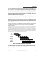
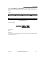
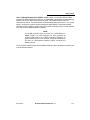
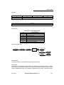
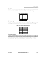
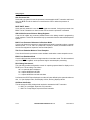
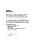
The logic required to support these three areas is contained in a debug module, which is
shown in the system block diagram in Figure 14-1.
COLDFIRE CPU
CORE
INTERNAL BUSES
DEBUG
MODULE
TRACE PORT
BDM PORT
DDATA, PST
DSCLK, DSI, DSO
Figure 14-1. Processor/Debug Module Interface
14.1 REAL-TIME TRACE
In the area of debug functions, one fundamental requirement is support for real-time trace
functionality (i.e., definition of the dynamic execution path). The ColdFire solution is to
include a parallel output port providing encoded processor status and data to an external
development system. This port is partitioned into two 4-bit nibbles: one nibble allows the
processor to transmit information concerning the execution status of the core (processor
status, PST[3:0]), while the other nibble allows data to be displayed (debug data,
DDATA[3:0]).
MOTOROLA
MCF5206 USERÕS MANUAL Rev 1.0
14-1
Debug Support
The processor status timing is synchronous with the processor clock (CLK) and the status
may not be related to the current bus transfer. Table 14-1 below shows the encodings of
these signals.
Table 14-1. Processor PST Definition
PST[3:0]
DEFINITION
0000
Continue execution
0001
Begin execution of an instruction
0010
Reserved
0011
Entry into user-mode
0100
Begin execution of PULSE or WDDATA instruction
0101
Begin execution of taken branch
0110
Reserved
0111
Begin execution of RTE instruction
1000
Begin 1-byte transfer on DData
1001
Begin 2-byte transfer on DData
1010
Begin 3-byte transfer on DData
1011
Begin 4-byte transfer on DData
1100
Exception processing
1101
Emulator-mode entry exception processing
1110
Processor is stopped, waiting for interrupt
1111
Processor is halted
These encodings are asserted for multiple cycles.
The processor status outputs can be used with an external image of the program to
completely track the dynamic execution path of the machine. The tracking of this dynamic
path is complicated by any change-of-flow operation. Within the ColdFire instruction set
architecture, most branch instructions are implemented using PC-relative addressing.
Accordingly, the external program image can determine branch target addresses.
Additionally, there are a number of instructions that use some type of variant addressing,
i.e., the calculation of the target instruction address is not PC-relative or absolute but
involves the use of a program-visible register.
The simplest example of a branch instruction using a variant addressing mode is the
compiled code for a C language case statement. Typically, the evaluation of this statement
uses the variable of an expression as an index into a table of offsets, where each offset
points to a unique case within the structure. For these types of change-of-flow operations,
the ColdFire processor uses the debug pins to output a sequence of information.
1. Identify a taken branch has been executed using the PST[3:0]=$5.
2. Using the PST pins, signal the target address is to be displayed on the DDATA pins.
The encoding identifies the number of bytes that are displayed and is optional.
3. The new target address is optionally available on subsequent cycles using the nibblewide DDATA port. The number of bytes of the target address displayed on this port is
a configurable parameter (2, 3, or 4 bytes).
14-2
MCF5206 USERÕS MANUAL Rev 1.0
MOTOROLA
Debug Support
The nibble-wide DDATA port includes two 32-bit storage elements for capturing the CPU
core bus information. These two elements effectively form a FIFO buffer connecting the core
bus to the external development system. The FIFO buffer captures variant branch target
addresses along with certain operand read/write data for eventual display on the DDATA
output port. The execution speed of the ColdFire processor is affected only when both
storage elements contain valid data waiting to be dumped onto the DDATA port. In this case,
the processor core stalls until one FIFO entry is available. In all other cases, data output on
the DDATA port does not impact execution speed.
From the processor core perspective, the PST outputs signal the first AGEX cycle of an
instructionÕs execution. Most single-cycle instructions begin and complete their execution
within a given machine cycle.
Because the processor status (PST[3:0]) values of $C, $D, $E, and $F define a multicycle
mode or a special operation, the PST outputs are driven with these values until the mode is
exited or the operation completed. All the remaining fields specify information that is updated
each machine cycle.
The status values of $8, $9, $A, and $B qualify the contents of the DDATA output bus. These
encodings are driven onto the PST port one machine cycle before the actual data is
displayed on DDATA.
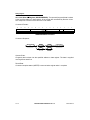
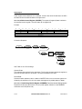
Figure14-3 shows the execution of an indirect JMP instruction with the lower 16 bits of the
target address being displayed on the DDATA output. In this diagram, the indirect JMP
branches to address Òtarget.Ó The processor internally forms the PST marker ($9) one cycle
before the address begins to appear on the DDATA port. The target address is displayed on
DDATA for four consecutive clocks, starting with the least-significant nibble. The processor
continues execution, unaffected by the DDATA bus activity.
Last
JMP (A0)
Target
Target + $4
Internal PST
Internal DDATA
PST Pins
DDATA Pins
DSOC
AGEX
DSOC
AGEX
IAG
IC
DSOC
AGEX
IAG
IC
DSOC
AGEX
$5
$9
$0
TARGET
$0
$0
3:0
7:4
11:8
$5
$9
$0
TARGET
$0
$0
3:0
7:4
15:12
11:8
15:12
Figure 14-2. Pipeline Timing Example (Debug Output)
The ColdFire instruction set architecture (ISA) includes a PULSE opcode. This opcode
generates a unique PST encoding when executed (PST = $4). This instruction can define
logic analyzer triggers for debug and/or performance analysis.
MOTOROLA
MCF5206 USERÕS MANUAL Rev 1.0
14-3
Debug Support
Additionally, a WDDATA opcode is supported that lets the processor core write any operand
(byte, word, longword) directly to the DDATA port, independent of any Debug module
configuration. This opcode also generates the special PST = $4 encoding when executed.
14.2 BACKGROUND-DEBUG MODE (BDM)
ColdFire 52xx processors support a modified version of the Background-Debug mode
(BDM) functionality found on MotorolaÕs CPU32 Family of parts. BDM implements a lowlevel system debugger in the microprocessor hardware. Communication with the
development system is handled via a dedicated, high-speed serial command interface
(BDM port).
Unless noted otherwise, the BDM functionality provided by ColdFire 52xx processors is a
proper subset of the CPU32 functionality. The main differences include the following:
¥ ColdFire implements the BDM controller in a dedicated hardware module. Although
some BDM operations do require the CPU to be halted (e.g., CPU register accesses),
other BDM commands such as memory accesses can be executed while the processor
is running.
¥ DSCLK, DSI, and DSO are treated as synchronous signals, where the inputs (DSCLK
and DSI) must meet the required input setup and hold timings, and the output (DSO) is
specified as a delay relative to the rising edge of the processor clock.
¥ On CPU32 parts, DSO could signal hardware that a serial transfer can start. ColdFire
clocking schemes restrict the use of this bit. Because DSO changes only when DSCLK
is high, DSO cannot be used to indicate the start of a serial transfer. The development
system should use either a free-running DSCLK or count the number of clocks in any
given transfer.
¥ The Read/Write System Register commands (RSREG/WSREG) have been replaced
by Read/Write Control Register commands (RCREG/WCREG). These commands use
the register coding scheme from the MOVEC instruction.
¥ Read/Write Debug Module Register commands (RDMREG/WDMREG) have been added to support Debug module register accesses.
¥ CALL and RST commands are not supported.
¥ Illegal command responses can be returned using the FILL and DUMP commands.
¥ For any command performing a byte-sized memory read operation, the upper 8 bits of
the response data are undefined. The referenced data is returned in the lower 8 bits of
the response.
¥ The debug module forces alignment for memory-referencing operations: long accesses
are forced to a 0-modulo-4 address; word accesses are forced to a 0-modulo-2
address. An address error response can no longer be returned.
14.2.1 CPU Halt
Although some BDM operations can occur in parallel with CPU operation, unrestricted BDM
operation requires the CPU to be halted. A number of sources can cause the CPU to halt,
including the following (as shown in order of priority):
14-4
MCF5206 USERÕS MANUAL Rev 1.0
MOTOROLA
Debug Support
1. The occurrence of the catastrophic fault-on-fault condition automatically halts the
processor. The halt status is posted on the PST port ($F).
2. The occurrence of a hardware breakpoint (reference subsection Section 14.3 RealTime Debug Support) can be configured to generate a pending halt condition in a
manner similar to the assertion of the BKPT signal. In some cases, the occurrence of
this type of breakpoint halts the processor in an imprecise manner. Once the hardware
breakpoint is asserted, the processor halts at the next sample point. See Section
14.3.2 Theory of Operation for more detail.
3. The execution of the HALT (also known as BGND on the 683xx devices) instruction
immediately suspends execution and posts the halt status ($F) on the PST outputs.
By default, this is a supervisor instruction and attempted execution while in user mode
generates a privilege-violation exception. A User Halt Enable (UHE) control bit is
provided in the Configuration/Status Register (CSR) to allow execution of HALT in
user mode.
4. The assertion of the BKPT input pin is treated as an pseudo-interrupt, i.e., the halt
condition is made pending until the processor core samples for halts/interrupts. The
processor samples for these conditions once during the execution of each instruction.
If there is a pending halt condition at the sample time, the processor suspends
execution and enters the halted state. The halt status ($F) is reflected in the PST
outputs.
The halt source is indicated in CSR[27:24]; for simultaneous halt conditions, the highest
priority source is indicated.
There are two special cases to be considered that involve the assertion of the BKPT pin.
After RSTI is negated, the processor waits for 16 clock cycles before beginning reset
exception processing. If the BKPT input pin is asserted within the first eight cycles after RSTI
is negated, the processor will enter the halt state, signaling that status on the PST outputs
($F). While in this state, all resources accessible via the Debug module can be referenced.
Once the system initialization is complete, the processor response to a BDM GO command
depends on the set of BDM commands performed while Òbreakpointed.Ó Specifically, if the
processorÕs PC register was loaded, the GO command causes the processor to exit the halt
state and pass control to the instruction address contained in the PC. In this case, the
normal reset exception processing is bypassed. Conversely, if the PC register was not
loaded, the GO BDM command causes the processor to exit the halt state and continue with
reset exception processing.
ColdFire 52xx processors also handle a special case with the assertion of BKPT while the
processor is stopped by execution of the STOP instruction. For this case when the BKPT is
asserted, the processor exits the stopped mode and enters the halted state. Once halted,
the standard BDM commands may be exercised. When the processor is restarted, it
continues with the execution of the next sequential instruction, i.e., the instruction following
the STOP opcode.
The debug module Configuration/Status Register (CSR) maintains status defining the
condition that caused the CPU to halt.
MOTOROLA
MCF5206 USERÕS MANUAL Rev 1.0
14-5
Debug Support
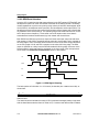
14.2.2 BDM Serial Interface
Once the CPU is halted and the halt status reflected on the PST outputs (PST[3:0]=$F), the
development system can send unrestricted commands to the Debug module. The Debug
module implements a synchronous protocol using a three-pin interface: development serial
clock (DSCLK), development serial input (DSI), and development serial output (DSO). The
development system serves as the serial communication channel master and is responsible
for generation of the clock (DSCLK). The operating range of the serial channel is DC to onehalf of the processor frequency. The channel uses a full duplex mode, where data is
transmitted and received simultaneously by both master and slave devices.
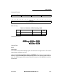
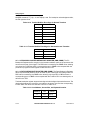
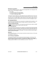
Both DSCLK and DSI are synchronous inputs and must meet input setup and hold times
with respect to CLK. DSCLK essentially acts as a pseudo Òclock enableÓ and is sampled on
the rising edge of CLK. If the setup time of DSCLK is met, then the internal logic transitions
on the rising edge of CLK, and DSI is sampled on the same CLK rising edge. The DSO
output is specified as a delay from the DSCLK-enabled CLK rising edge. All events in the
Debug moduleÕs serial state machine are based on the rising edge of the microprocessor
clock. Refer to the Electrical Characteristics section of this manual.
CLK
DSCLK
DSI
DSO
Figure 14-3. BDM Signal Sampling
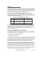
The basic packet of information is a 17-bit word (16 data bits plus a status/control bit), as
shown here.
16
S/C
15
0
DATA FIELD [15:0]
Status/Control
The status/control bit indicates the status of CPU-generated messages (always single word
with the data field encoded as listed in Table 14-2). Command and data transfers initiated
14-6
MCF5206 USERÕS MANUAL Rev 1.0
MOTOROLA
Debug Support
by the development system should clear bit 16. The current implementation ignores this bit;
however, Motorola has reserved this bit for future enhancements.
Table 14-2. CPU-Generated Message Encoding
S/C BIT
0
0
1
1
1
DATA
xxxx
$FFFF
$0000
$0001
$FFFF
MESSAGE TYPE
Valid data transfer
Command complete; status OK
Not ready with response; come again
TEA-terminated bus error cycle; data invalid
Illegal command
Data Field
The data field contains the message data to be communicated between the development
system and the Debug module.
14.2.3 BDM Command Set
ColdFire 52xx processors support a subset of BDM instructions from the current 683xx parts
as well as extensions to provide access to new hardware features.
14.2.3.1 BDM COMMAND SET SUMMARY. The BDM command set is summarized in
Table 14-3. Subsequent paragraphs contain detailed descriptions of each command.
Table 14-3. BDM Command Summary
COMMAND
MNEMONIC
Read A/D Register
RAREG/RDREG
Write A/D Register
WAREG/WDREG
Read Memory Location
READ
Write Memory Location
WRITE
Dump Memory Block
DUMP
Fill Memory Block
FILL
Resume Execution
GO
No Operation
NOP
Read Control Register
Write Control Register
Read Debug Module Register
Write Debug
Module Register
RCREG
WCREG
RDMREG
DESCRIPTION
CPUIMPACT1
Read the selected address or data register and return the result
Halted
via the serial BDM interface
The data operand is written to the specified address or data
Halted
register via the serial BDM interface
Read the sized data at the memory location specified by the
Cycle
longword address
Steal
Cycle
Write the operand data to the memory location specified by the
longword address
Steal
Used in conjunction with the READ command to dump large
blocks of memory. An initial READ is executed to set up the
Cycle
starting address of the block and to retrieve the first result.
Steal
Subsequent operands are retrieved with the DUMP command.
Used in conjunction with the WRITE command to fill large
blocks of memory. An initial WRITE is executed to set up the
Cycle
starting address of the block and to supply the first operand.
Steal
Subsequent operands are written with the FILL command.
The pipeline is flushed and refilled before resuming instruction
Halted
execution at the current PC
NOP performs no operation and may be used as a null
Parallel
command
Read the system control register
Halted
Write the operand data to the system control register
Halted
Read the Debug module register
Parallel
WDMREG
Write the operand data to the Debug module register
MOTOROLA
MCF5206 USERÕS MANUAL Rev 1.0
Halted
14-7
Debug Support
Table 14-3. BDM Command Summary (Continued)
COMMAND
MNEMONIC
CPUIMPACT1
DESCRIPTION
NOTE:
1.
General command effect and/or requirements on CPU operation:
Halted - The CPU must be halted to perform this command
Steal - Command generates a bus cycle which is interleaved with CPU accesses
Parallel - Command is executed in parallel with CPU activity
Refer to command summaries for detailed operation descriptions.
14.2.3.2 COLDFIRE BDM COMMANDS. All ColdFire Family BDM commands include a 16bit operation word followed by an optional set of one or more extension words.
15
10
OPERATION
9
0
6
5
4
3
R/W
OP SIZE
EXTENSION WORD(S)
8
7
0
0
A/D
2
0
REGISTER
Operation Field
The operation field specifies the command.
R/W Field
The R/W field specifies the direction of operand transfer. When the bit is set, the transfer is
from the CPU to the development system. When the bit is cleared, data is written to the CPU
or to memory from the development system.
Operand Size
For sized operations, this field specifies the operand data size. All addresses are expressed
as 32-bit absolute values. The size field is encoded as listed in Table 14-4.
Table 14-4. BDM Size Field Encoding
ENCODING
00
01
10
11
OPERAND SIZE
Byte
Word
Long
Reserved
Address / Data (A/D) Field
The A/D field is used in commands that operate on address and data registers in the
processor. It determines whether the register field specifies a data or address register. A one
indicates an address register; zero, a data register.
Register Field
In commands that operate on processor registers, this field specifies which register is
selected. The field value contains the register number.
14-8
MCF5206 USERÕS MANUAL Rev 1.0
MOTOROLA
Debug Support
Extension Word(s) (as required):
Certain commands require extension words for addresses and/or immediate data.
Addresses require two extension words because only absolute long addressing is permitted.
Immediate data can be either one or two words in length; byte and word data each require
a single extension word; longword data requires two words. Both operands and addresses
are transferred by most significant word first. In the following descriptions of the BDM
command set, the optional set of extension words are defined as the ÒOperand Data.Ó
14.2.3.3 Command Sequence Diagram. A command sequence diagram (see Figure
14-4) illustrates the serial bus traffic for each command. Each bubble in the diagram
represents a single 17-bit transfer across the bus. The top half in each diagram corresponds
to the data transmitted by the development system to the debug module; the bottom half
corresponds to the data returned by the debug module in response to the development
system commands. Command and result transactions are overlapped to minimize latency.
The cycle in which the command is issued contains the development system command
mnemonic (in this example, Òread memory locationÓ). During the same cycle, the debug
module responds with either the lowest order results of the previous command or with a
command complete status (if no results were required).
During the second cycle, the development system supplies the high-order 16 bits of the
memory address. The debug module returns a Ònot readyÓ response($10000) unless the
received command was decoded as unimplemented, in which case the response data is the
illegal command ($1FFFF) encoding. If an illegal command response occurs, the
development system should retransmit the command.
NOTE
The Ònot readyÓ response is ignored unless a memory bus cycle
is in progress. Otherwise, the debug module can accept a new
serial transfer after eight system clock periods.
In the third cycle, the development system supplies the low-order 16 bits of a memory
address. The debug module always returns the Ònot readyÓ response in this cycle. At the
completion of the third cycle, the debug module initiates a memory read operation. Any
serial transfers that begin while the memory access is in progress return the Ònot readyÓ
response.
Results are returned in the two serial transfer cycles following the completion of memory
access. The data transmitted to the debug module during the final transfer is the opcode for
the following command. Should a memory access generate a bus error, an error status
($10001) is returned in place of the result data.
MOTOROLA
MCF5206 USERÕS MANUAL Rev 1.0
14-9
Debug Support
COMMANDS TRANSMITTED TO THE DEBUG MODULE
COMMAND CODE TRANSMITTED DURING THIS CYCLE
HIGH-ORDER 16 BITS OF MEMORY ADDRESS
LOW-ORDER 16 BITS OF MEMORY ADDRESS
NONSERIAL-RELATED ACTIVITY
SEQUENCE TAKEN IF
OPERATION HAS NOT
COMPLETED
READ (LONG)
???
MS ADDR
"NOT READY"
LS ADDR
"NOT READY"
XXX
"ILLEGAL"
NEXT CMD
"NOT READY"
READ
MEMORY
LOCATION
XXX
"NOT READY"
NEXT
COMMAND
CODE
XXXXX
XXX
MS RESULT
NEXT CMD
LS RESULT
XXX
BERR
NEXT CMD
"NOT READY"
DATA UNUSED FROM
THIS TRANSFER
SEQUENCE TAKEN IF BUS
ERROR OCCURS ON
MEMORY ACCESS
SEQUENCE TAKEN IF
ILLEGAL COMMAND
IS RECEIVED BY DEBUG MODULE
HIGH- AND LOW-ORDER
16 BITS OF RESULT
RESULTS FROM PREVIOUS COMMAND
RESPONSES FROM THE DEBUG MODULE
Figure 14-4. Command Sequence Diagram
14.2.3.4 Command Set Descriptions. The BDM command set is summarized in Table
14-3.
Note
All the accompanying valid BDM results are defined with the
most significant bit of the 17-bit response (S/C) as 0. Invalid
command responses (Not Ready; TEA-terminated bus cycle; Illegal Command) return a 1 in the most significant bit of the 17bit response (S/C).
Motorola reserves unassigned command opcodes for future expansion. All unused command formats within any revision level will perform a NOP and return the ILLEGAL command response.
14-10
MCF5206 USERÕS MANUAL Rev 1.0
MOTOROLA
Debug Support
14.2.3.4.1 Read A/D Register (RAREG/RDREG). Read the selected address or data
register and return the 32-bit result. A bus error response is returned if the CPU core is not
halted.
Formats:
15
14
13
12
11
10
$2
9
8
7
6
$1
5
4
$8
3
2
A/D
1
0
REGISTER
RAREG/RDREG Command
15
14
13
12
11
10
9
8
7
6
5
4
3
2
1
0
DATA [31:16]
DATA [15:0]
RAREG/RDREG Result
Command Sequence:
RAREG/RDREG
???
XXX
MS RESULT
XXX
BERR
NEXT CMD
LS RESULT
NEXT CMD
"NOT READY
Operand Data:
None
Result Data:
The contents of the selected register are returned as a longword value. The data is returned
most significant word first.
MOTOROLA
MCF5206 USERÕS MANUAL Rev 1.0
14-11
Debug Support
14.2.3.4.2 Write A/D Register (WAREG/WDREG). The operand (longword) data is written
to the specified address or data register. All 32 register bits are altered by the write. A bus
error response is returned if the CPU core is not halted.
Command Formats:
15
14
13
12
11
10
$2
9
8
7
6
$0
5
$8
4
3
A/D
2
1
0
REGISTER
DATA [31:16]
DATA [15:0]
WAREG/WDREG Command
Command Sequence:
WDREG/WAREG
???
MS DATA
"NOT READY"
XXX
BERR
LS DATA
"NOT READY"
NEXT CMD
"CMD COMPLETE"
NEXT CMD
"NOT READY"
Operand Data:
Longword data is written into the specified address or data register. The data is supplied
most significant word first.
Result Data:
Command complete status ($0FFFF) is returned when register write is complete.
14-12
MCF5206 USERÕS MANUAL Rev 1.0
MOTOROLA
Debug Support
14.2.3.4.3 Read Memory Location (READ). Read the operand data from the memory
location specified by the longword address. The address space is defined by the contents
of the low-order 5 bits {TT, TM} of the address attribute register (AATR). The hardware
forces the low-order bits of the address to zeros for word and longword accesses to ensure
that operands are always accessed on natural boundaries: words on 0-modulo-2 addresses,
longwords on 0-modulo-4 addresses.
Formats:
15
14
13
12
11
10
$1
9
8
7
6
$9
5
4
3
2
$0
1
0
1
0
1
0
1
0
1
0
1
0
$0
ADDRESS [31:16]
ADDRESS [15:0]
Byte READ Command
15
X
14
X
13
X
12
X
11
X
10
X
9
X
8
X
7
6
5
4
3
DATA [7:0]
2
5
4
2
Byte READ Result
15
14
13
12
11
10
$1
9
8
7
6
$9
3
$4
$0
ADDRESS [31:16]
ADDRESS [15:0]
Word READ Command
15
14
13
12
11
10
9
8
7
DATA [15:0]
6
5
4
3
2
5
4
3
2
Word READ Result
15
14
13
12
11
10
$1
9
8
7
6
$9
$8
$0
ADDRESS [31:16]
ADDRESS [15:0]
Long READ Command
15
14
13
12
11
10
9
8
7
DATA [31:16]
DATA [15:0]
6
5
4
3
2
Long READ Result
MOTOROLA
MCF5206 USERÕS MANUAL Rev 1.0
14-13
Debug Support
Command Sequence:
READ (B/W)
???
MS ADDR
"NOT READY"
LS ADDR
"NOT READY"
READ
MEMORY
LOCATION
XXX
"NOT READY"
XXXCMD
NEXT
RESULT
XXX
BERR
READ (LONG)
???
MS ADDR
"NOT READY"
LS ADDR
"NOT READY"
READ
MEMORY
LOCATION
NEXT CMD
"NOT READY"
XXX
"NOT READY"
XXX
XXX
MS RESULT
XXX
BERR
NEXT CMD
LS RESULT
NEXT CMD
"NOT READY"
Operand Data:
The single operand is the longword address of the requested memory location.
Result Data:
The requested data is returned as either a word or longword. Byte data is returned in the
least significant byte of a word result, with the upper byte undefined. Word results return 16
bits of significant data; longword results return 32 bits.
A successful read operation returns data bit 16 cleared. If a bus error is encountered, the
returned data is $10001.
14-14
MCF5206 USERÕS MANUAL Rev 1.0
MOTOROLA
Debug Support
14.2.3.4.4 Write Memory Location (WRITE). Write the operand data to the memory
location specified by the longword address. The address space is defined by the contents
of the low-order 5 bits {TT, TM} of the address attribute register (AATR). The hardware
forces the low-order bits of the address to zeros for word and longword accesses to ensure
that operands are always accessed on natural boundaries: words on 0-modulo-2 addresses,
longwords on 0-modulo-4 addresses.
Formats:
15
14
13
12
11
10
$1
9
8
7
6
$8
5
4
3
2
$0
1
0
1
0
1
0
$0
ADDRESS [31:16]
ADDRESS [15:0]
X
X
X
X
X
X
X
X
DATA [7:0]
Byte WRITE Command
15
14
13
12
11
10
$1
9
8
7
6
$8
5
4
3
2
$4
$0
ADDRESS [31:16]
ADDRESS [15:0]
DATA [15:0]
Word WRITE Command
15
14
13
$1
12
11
10
9
8
7
$8
6
5
$8
4
3
2
$0
ADDRESS [31:16]
ADDRESS [15:0]
DATA [31:16]
DATA [15:0]
Long WRITE Command
MOTOROLA
MCF5206 USERÕS MANUAL Rev 1.0
14-15
Debug Support
Command Sequence:
WRITE (B/W)
???
MS ADDR
"NOT READY"
LS ADDR
"NOT READY"
DATA
"NOT READY"
WRITE
MEMORY
LOCATION
XXX
"NOT READY"
XXX CMD
NEXT
"CMD COMPLETE
XXX
BERR
NEXT CMD
"NOT READY"
WRITE (LONG)
???
MS ADDR
"NOT READY"
LS ADDR
"NOT READY"
MS DATA
"NOT READY"
LS DATA
"NOT READY"
WRITE
MEMORY
LOCATION
XXX
"NOT READY"
XXX CMD
NEXT
"CMD COMPLETE
XXX
BERR
NEXT CMD
"NOT READY"
Operand Data:
Two operands are required for this instruction. The first operand is a longword absolute address that specifies a location to which the operand data is to be written. The second operand is the data. Byte data is transmitted as a 16-bit word, justified in the least significant byte;
16- and 32-bit operands are transmitted as 16 and 32 bits, respectively.
Result Data:
Successful write operations return a status of $0FFFF. A bus error on the write cycle is indicated by the assertion of bit 16 in the status message and by a data pattern of $0001.
14-16
MCF5206 USERÕS MANUAL Rev 1.0
MOTOROLA
Debug Support
14.2.3.4.5 Dump Memory Block (DUMP). DUMP is used in conjunction with the READ
command to dump large blocks of memory. An initial READ is executed to set up the starting
address of the block and to retrieve the first result. The DUMP command retrieves
subsequent operands. The initial address is incremented by the operand size (1, 2, or 4) and
saved in a temporary register (Address Breakpoint High (ABHR)). Subsequent DUMP
commands use this address, perform the memory read, increment it by the current operand
size, and store the updated address in ABHR.
NOTE
The DUMP command does not check for a valid address in
ABHRÑDUMP is a valid command only when preceded by
another DUMP, NOP or by a READ command. Otherwise, an
illegal command response is returned. The NOP command can
be used for intercommand padding without corrupting the
address pointer.
The size field is examined each time a DUMP command is given, allowing the operand size
to be dynamically altered.
MOTOROLA
MCF5206 USERÕS MANUAL Rev 1.0
14-17
Debug Support
Command Formats:
15
14
13
12
11
10
$1
9
8
7
6
$D
5
4
3
2
$0
1
0
1
0
1
0
1
0
1
0
1
0
$0
Byte DUMP Command
15
14
13
12
11
10
9
8
X
X
X
X
X
X
X
X
7
6
5
4
3
2
DATA [7:0]
Byte DUMP Result
15
14
13
12
11
10
$1
9
8
7
6
$D
5
4
3
2
$4
$0
Word DUMP Command
15
14
13
12
11
10
9
8
7
DATA [15:0]
6
5
4
3
2
5
4
3
2
Word DUMP Result
15
14
13
12
11
10
$1
9
8
7
6
$D
$8
$0
Long DUMP Command
15
14
13
12
11
10
9
8
7
DATA [31:16]
6
5
4
3
2
DATA [15:0]
Long DUMP Result
14-18
MCF5206 USERÕS MANUAL Rev 1.0
MOTOROLA
Debug Support
Command Sequence:
DUMP (B/W)
???
READ
MEMORY
LOCATION
XXX
"NOT READY"
NEXT CMD
RESULT
XXX
"ILLEGAL"
DUMP (LONG)
???
NEXT CMD
"NOT READY"
READ
MEMORY
LOCATION
XXX
BERR
XXX
"NOT READY"
NEXT CMD
MS RESULT
XXX
"ILLEGAL"
NEXT CMD
"NOT READY"
NEXT CMD
"NOT READY"
XXX
BERR
NEXT CMD
LS RESULT
NEXT CMD
"NOT READY"
Operand Data:
None
Result Data:
Requested data is returned as either a word or longword. Byte data is returned in the least
significant byte of a word result. Word results return 16 bits of significant data; longword results return 32 bits. Status of the read operation is returned as in the READ command:
$0xxxx for success, $10001 for a bus error.
MOTOROLA
MCF5206 USERÕS MANUAL Rev 1.0
14-19
Debug Support
14.2.3.4.6 Fill Memory Block (FILL). FILL is used in conjunction with the WRITE
command to fill large blocks of memory. An initial WRITE is executed to set up the starting
address of the block and to supply the first operand. The FILL command writes subsequent
operands. The initial address is incremented by the operand size (1, 2, or 4) and is saved in
ABHR after the memory write. Subsequent FILL commands use this address, perform the
write, increment it by the current operand size, and store the updated address in ABHR.
NOTE
The FILL command does not check for a valid address in
ABHRÑFILL is a valid command only when preceded by
another FILL, NOP or by a WRITE command. Otherwise, an
illegal command response is returned. The NOP command can
be used for intercommand padding without corrupting the
address pointer.
The size field is examined each time a FILL command is processed, allowing the operand
size to be altered dynamically.
Formats:
15
14
13
12
11
10
$1
X
X
9
8
7
6
$C
X
X
X
X
5
4
3
2
$0
X
1
0
1
0
1
0
$0
X
DATA [7:0]
Byte FILL Command
15
14
13
12
11
10
$1
9
8
7
6
$C
5
4
3
2
$4
$0
DATA [15:0]
Word FILL Command
15
14
13
$1
12
11
10
9
8
7
$C
6
5
$8
4
3
2
$0
DATA [31:16]
DATA [15:0]
Long FILL Command
14-20
MCF5206 USERÕS MANUAL Rev 1.0
MOTOROLA
Debug Support
Command Sequence:
FILL (B/W)
???
MS DATA
"NOT READY"
LS DATA
"NOT READY"
XXX
"ILLEGAL"
NEXT CMD
"NOT READY"
WRITE
MEMORY
LOCATION
XXX
"NOT READY"
NEXT CMD
"CMD COMPLETE"
NEXT CMD
"NOT READY"
XXX
BERR
FILL (LONG)
???
DATA
"NOT READY"
WRITE
MEMORY
LOCATION
XXX
"ILLEGAL"
NEXT CMD
"NOT READY"
XXX
"NOT READY"
NEXT CMD
"CMD COMPLETE"
NEXT CMD
"NOT READY"
XXX
BERR
Operand Data:
A single operand is data to be written to the memory location. Byte data is transmitted as a
16-bit word, justified in the least significant byte; 16- and 32-bit operands are transmitted as
16 and 32 bits, respectively.
Result Data:
Status is returned as in the WRITE command: $0FFFF for a successful operation and
$10001 for a bus error during a write.
14.2.3.4.7 Resume Execution (GO). The pipeline is flushed and refilled before resuming
normal instruction execution. Prefetching begins at the current PC and current privilege
level. If either the PC or SR is altered during BDM, the updated value of these registers is
used when prefetching begins.
Formats:
15
14
13
$0
12
11
10
9
8
7
6
$C
5
$0
4
3
2
1
0
$0
GO Command
MOTOROLA
MCF5206 USERÕS MANUAL Rev 1.0
14-21
Debug Support
Command Sequence:
GO
???
NEXT CMD
"CMD COMPLETE"
Operand Data:
None
Result Data:
The Òcommand completeÓ response ($0FFFF) is returned during the next shift operation.
14.2.3.4.8 No Operation (NOP). NOP performs no operation and can be used as a null
command, where required.
Formats:
15
12
$0
11
8
7
$0
4
$0
3
0
$0
NOP Command
Command Sequence:
NOP
???
NEXT CMD
"CMD COMPLETE"
Operand Data:
None
Result Data:
The Òcommand completeÓ response ($0FFFF) is returned during the next shift operation.
14.2.3.4.9 Read Control Register (RCREG). Read the selected control register and return
the 32-bit result. Accesses to the processor/memory control registers are always 32 bits in
size, regardless of the implemented register width. The second and third words of the
command effectively form a 32-bit address the debug module uses to generate a special bus
cycle to access the specified control register. The 12-bit Rc field is the same as that used
by the MOVEC instruction.
14-22
MCF5206 USERÕS MANUAL Rev 1.0
MOTOROLA
Debug Support
Formats
15
14
13
12
11
10
$2
$0
9
8
7
6
$9
$0
5
4
3
2
$8
$0
$0
1
0
1
0
$0
$0
RC
RCREG Command
15
14
13
12
11
10
9
8
7
6
5
4
3
2
DATA [31:16]
DATA [15:0]
RCREG Result
Rc encoding:
Table 14-5. Control Register Map
Rc
$002
$004
$005
$801
$80E
$80F
$C04
$C0F
REGISTER DEFINITION
Cache Control Register (CACR)
Access Control Unit 0 (ACR0)
Access Control Unit 1 (ACR1)
Vector Base Register (VBR)
Status Register (SR)
Program Counter (PC)
RAM Base Address Register (RAMBAR)
Module Base Address Register (MBAR)
Command Sequence:
RCREG
???
EXT WORD
"NOT READY"
EXT WORD
"NOT READY"
READ
MEMORY
LOCATION
XXX
"NOT READY"
XXX
MS RESULT
NEXT CMD
LS RESULT
XXX
BERR
NEXT CMD
"NOT READY"
Operand Data:
The single operand is the 32-bit Rc control register select field.
Result Data:
The contents of the selected control register are returned as a longword value. The data is
returned by most significant word first. For those control register widths less than 32 bits,
only the implemented portion of the register is guaranteed to be correct. The remaining bits
MOTOROLA
MCF5206 USERÕS MANUAL Rev 1.0
14-23
Debug Support
of the longword are undefined. As an example, a read of the 16-bit SR will return the SR in
the lower word and undefined data in the upper word.
14.2.3.4.10 Write Control Register (WCREG). The operand (longword) data is written to
the specified control register. The write alters all 32 register bits.
Formats:
15
14
13
12
11
$2
$0
10
9
8
7
6
$8
$0
5
4
$8
$0
$0
3
2
1
0
$0
$0
Rc
DATA [31:16]
DATA [15:0]
WCREG Command
Command Sequence:
WCREG
???
EXT WORD
"NOT READY"
EXT WORD
"NOT READY"
MS DATA
"NOT READY"
LS DATA
"NOT READY"
WRITE
MEMORY
LOCATION
XXX
"NOT READY"
XXX CMD
NEXT
"CMD COMPLETE
XXX
BERR
NEXT CMD
"NOT READY"
See Table 14-6 for Rc encodings.
Operand Data:
Two operands are required for this instruction. The first long operand selects the register to
which the operand data is to be written. The second operand is the data.
Result Data:
Successful write operations return a status of $0FFFF. Bus errors on the write cycle are indicated by the assertion of bit 16 in the status message and by a data pattern of $0001.
14.2.3.4.11 Read Debug Module Register (RDMREG). Read the selected Debug Module
Register and return the 32-bit result. The only valid register selection for the RDMREG
command is the CSR (DRc = $0).
14-24
MCF5206 USERÕS MANUAL Rev 1.0
MOTOROLA
Debug Support
Command Formats:
15
14
13
12
11
10
$2
9
8
7
6
$D
5
4
3
2
$8
1
0
1
0
DRc
RDMREG BDM Command
15
14
13
12
11
10
9
8
7
6
5
4
3
2
DATA [31:16]
DATA [15:0]
RDMREG BDM Result
DRc encoding:
Table 14-6. Definition of DRc Encoding - Read
DRC[3:0]
DEBUG REGISTER DEFINITION
MNEMONIC
INITIAL
STATE
$0
Configuration/Status
CSR
$0
$1-$F
Reserved
-
Ð
Command Sequence:
RDMREG
???
XXX
MS RESULT
NEXT CMD
LS RESULT
XXX
"ILLEGAL"
NEXT CMD
"NOT READY"
Operand Data:
None
Result Data:
The contents of the selected debug register are returned as a longword value. The data is
returned most significant word first.
14.2.3.4.12 Write Debug Module Register (WDMREG). The operand (longword) data is
written to the specified Debug Module Register. All 32 bits of the register are altered by the
write. The DSCLK signal must be inactive while CPU execution of the WDEBUG instruction
is performed.
MOTOROLA
MCF5206 USERÕS MANUAL Rev 1.0
14-25
Debug Support
Command Format:
15
14
13
12
11
10
$2
9
8
7
$C
6
5
4
3
2
$8
1
0
DRC
DATA [31:16]
DATA [15:0]
WDMREG BDM Command
DRc encoding:
Table 14-7. Definition of DRc Encoding - Write
DRc[3:0]
$0
$1-$5
DEBUG REGISTER DEFINITION
Configuration/Status
MNEMONIC
INITIAL
STATE
CSR
$0
-
Ð
Reserved
$6
Bus Attributes And Mask
AATR
$0005
$7
Trigger Definition
TDR
$0
$8
PC Breakpoint
PBR
Ð
$9
PC Breakpoint Mask
PBMR
Ð
Ð
Ð
$A-$B
Reserved
$C
Operand Address High Breakpoint
ABHR
Ð
$D
Operand Address Low Breakpoint
ABLR
Ð
$E
Data Breakpoint
DBR
Ð
$F
Data Breakpoint Mask
DBMR
Ð
Command Sequence:
WDMREG
???
MS DATA
"NOT READY"
LS DATA
"NOT READY"
XXX
"ILLEGAL"
NEXT CMD
"NOT READY"
NEXT CMD
"CMD COMPLETE"
Operand Data:
Longword data is written into the specified debug register. The data is supplied most significant word first.
Result Data:
Command complete status ($0FFFF) is returned when register write is complete.
14.2.3.4.13 Unassigned Opcodes. Motorola reserves unassigned command opcodes . All
unused command formats within any revision level will perform a NOP and return the
ILLEGAL command response.
14-26
MCF5206 USERÕS MANUAL Rev 1.0
MOTOROLA
Debug Support
14.3 REAL-TIME DEBUG SUPPORT
ColdFire processors provide support for the debug of real-time applications. For these types
of embedded systems, the processor cannot be halted during debug but must continue to
operate. The foundation of this area of debug support is that while the processor cannot be
halted to allow debugging, the system can tolerate small intrusions into the real-time
operation.
As discussed in the previous subsection, the debug module provides a number of hardware
resources to support various hardware breakpoint functions. Specifically, three types of
breakpoints are supported: PC with mask, operand address range, and data with mask.
These three basic breakpoints can be configured into one- or two-level triggers with the
exact trigger response also programmable.
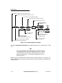
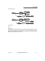
14.3.1 Programming Model
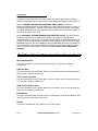
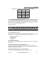
In addition to the existing BDM commands that provide access to the processorÕs registers
31
15
15
0
7
ABLR
ABHR
ADDRESS
BREAKPOINT REGISTERS
AATR
ADDRESS ATTRIBUTE
TRIGGER REGISTER
PBR
PBMR
PC BREAKPOINT
REGISTERS
DBR
DBMR
DATA BREAKPOINT
REGISTERS
0
TDR
CSR
TRIGGER DEFINITION
REGISTER
CONFIGURATION/STATUS
REGISTER
Figure 14-5. Debug Programming Model
and the memory subsystem, the Debug module contains a number of registers to support
the required functionality. All of these registers are treated as 32-bit quantities, regardless
of the actual number of bits in the implementation. The registers, known as the Debug
Control Registers (DRc), are addressed using a 4-bit value as part of two new BDM
commands (WDREG, RDREG).
These registers are also accessible from the processorÕs supervisor programming model
through the execution of the WDEBUG instruction (Figure 14-5 illustrates the debug module
programming model). Thus, the breakpoint hardware within the debug module can be
accessed by the external development system using the serial interface, or by the operating
system running on the processor core. It is the responsibility of the software to guarantee
that all accesses to these resources are serialized and logically consistent. The hardware
MOTOROLA
MCF5206 USERÕS MANUAL Rev 1.0
14-27
Debug Support
provides a locking mechanism in the CSR to allow the external development system to
disable any attempted writes by the processor to the Breakpoint Registers (setting IPW =1).
14.3.1.1 ADDRESS BREAKPOINT REGISTERS (ABLR, ABHR). The Address
Breakpoint Registers define an upper (ABHR) and a lower (ABLR) boundary for a region in
the operand logical address space of the processor that can be used as part of the trigger.
The ABLR and ABHR values are compared with the ColdFire CPU core address signals, as
defined by the setting of the TDR.
14.3.1.2 ADDRESS ATTRIBUTE BREAKPOINT REGISTER (AATR). The AATR defines
the address attributes and a mask to be matched in the trigger. The AATR value is
compared with the ColdFire CPU core address attribute signals, as defined by the setting of
the TDR. The AATR is accessible in supervisor mode as debug control register $6 using the
WDEBUG instruction and via the BDM port using the WDMREG command. The lower five
bits of the AATR are also used for BDM command definition to define the address space for
memory references as described in subsection 14.3.2.1 Reuse of the Debug Module
Hardware.
15
RM
14
13
SZM
12
11
TTM
10
8
TMM
7
R
6
5
SZ
4
3
2
0
TT
TM
AATR Bit Definitions
RMÐRead/Write Mask
This field corresponds to the R-field. When this bit is set, R is ignored in address
comparisons.
SZMÐSize Mask
This field corresponds to the SZ field. When a bit in this field is set, the corresponding bit in
SZ is ignored in address comparisons.
TTMÐTransfer Type Mask
This field corresponds to the TT field. When a bit in this field is set, the corresponding bit in
TT is ignored in address comparisons.
TMMÐTransfer Modifier Mask
This field corresponds to the TM field. When a bit in this field is set, the corresponding bit in
TM is ignored in address comparisons.
RÐRead/Write
This field is compared with the ColdFire CPU core R/W signal. A high level indicates a read
cycle and a low level indicates a write cycle.
SZÐSize
This field is compared with the ColdFire CPU core SIZ signals.
14-28
MCF5206 USERÕS MANUAL Rev 1.0
MOTOROLA
Debug Support
SZÑ-Size
This field is compared to the ColdFire CPU core SIZ signals. These signals indicate the data
size for the bus transfer. Table 14-8 shows the definitions for the SZ encodings.
Table 14-8. SZ Encodings
SZ[1:0]
TRANSFER SIZE
00
Longword (4 bytes)
01
Byte
10
Word (2 bytes)
11
Line (4 x 4 bytes)
TTÐTransfer Type
This field is compared with the ColdFire CPU core TT signals. These signals indicate the
transfer type for the bus transfer. Table 14-9 shows the definition of the TT encodings.
Table 14-9. Transfer Type Encodings
TT[1:0]
TRANSFER TYPE
00
Normal Access
01
Reserved
10
Alternate and Debug
Access
11
Acknowledge Access
TMÐTransfer Modifier
This field is compared with the ColdFire CPU core TM signals. These signals provide supplemental information for each transfer type. Table 14-10 shows encodings for normal transfers and Table 14-11 shows the encodings for alternate and debug access transfers. For
interrupt-acknowledge transfers, the TM [2:0] signals indicate the interrupt level being
acknowledged. For CPU space transfers initiated by a MOVEC instruction or a debug
MOTOROLA
MCF5206 USERÕS MANUAL Rev 1.0
14-29
Debug Support
WCREG command, TT[1:0] = 11 and TM[2:0] = 000. For breakpoint-acknowledge transfers,
the TM signals are low.
Table 14-10. Transfer Modifier Encodings for Normal Transfers
TM[2:0]
TRANSFER MODIFIER
000
Reserved
001
User Data Access
010
User Code Access
011 - 100
Reserved
101
Supervisor Data Access
110
Supervisor Code Access
111
Reserved
Table 14-11. Transfer Modifier Encodings for Alternate Access Transfers
TM[2:0]
TRANSFER MODIFIER
000 - 100, 111
Reserved
101
Emulator Mode Data Access
110
Emulator Mode Code Access
14.3.1.3 PROGRAM COUNTER BREAKPOINT REGISTER (PBR, PBMR). The PC
Breakpoint Registers define a region in the instruction address space of the processor that
can be used as part of the trigger. The PBR value is masked by the PBMR value, allowing
only those bits in PBR that have a corresponding zero in PBMR to be compared with the
processorÕs program counter register as defined in the TDR.
14.3.1.4 DATA BREAKPOINT REGISTER (DBR, DBMR). The Data Breakpoint Registers
define a specific data pattern that can be used as part of the trigger into Debug mode.The
DBR value is masked by the DBMR value, allowing only those bits in DBR that have a
corresponding zero in DBMR to be compared with the ColdFire CPU core data signals, as
defined in the TDR.
The data breakpoint register supports both aligned and misaligned operand references. The
relationship between the processor core address, the access size, and the corresponding
location within the 32-bit core data bus is shown in Table 14-12.
Table 14-12. Core Address, Access Size, and Operand Location
14-30
CORE
ADDRESS[1:0]
ACCESS
SIZE
OPERAND
LOCATION
00
Byte
Data[31:24]
01
Byte
Data[23:16]
MCF5206 USERÕS MANUAL Rev 1.0
MOTOROLA
Debug Support
Table 14-12. Core Address, Access Size, and Operand Location
CORE
ADDRESS[1:0]
ACCESS
SIZE
OPERAND
LOCATION
10
Byte
Data[15:8]
11
Byte
Data[7:0]
0-
Word
Data[31:16]
1-
Word
Data[15:0]
--
Long
Data[31:0]
14.3.1.5 TRIGGER DEFINITION REGISTER (TDR). The TDR configures the operation of
the hardware breakpoint logic within the Debug module and controls the actions taken under
the defined conditions. The breakpoint logic can be configured as a one- or two-level trigger,
where bits [29:16] of the TDR define the 2nd level trigger, bits [13:0] define the first level
trigger, and bits [31:30] define the trigger response.
Reset clears the TDR.
31
30
TRC
15
14
00
29
EBL
13
EBL
28
27
26
25
EDLW EDWL EDWU EDLL
12
11
10
9
EDLW EDWL EDWU EDLL
24
23
22
EDLM EDUM EDUU
8
7
6
EDLM EDUM EDUU
21
DI
20
EAI
19
EAR
18
EAL
17
EPC
16
PCI
5
4
3
2
1
0
DI
EAI
EAR
EAL
EPC
PCI
TDR Bit Definitions
TRCÐTrigger Response Control
The trigger response control determines how the processor is to respond to a completed
trigger condition. The trigger response is always displayed on the DDATA pins.
00=displayed on DDATA pins only
01=processor halt
10=debug interrupt
11=reserved
EBLÐEnable Breakpoint Level
If set, this bit serves as the global enable for the breakpoint trigger. If cleared, all breakpoints
are disabled.
EDLWÐEnable Data Breakpoint for the Data Longword
If set, this bit enables the data breakpoint based on the core data bus (KD) KD[31:0]
longword. The assertion of any of the ED bits enables the data breakpoint. If all bits are
cleared, the data breakpoint is disabled.
EDWLÐEnable Data Breakpoint for the Lower Data Word
If set, this bit enables the data breakpoint based on the KD[15:0] word.
MOTOROLA
MCF5206 USERÕS MANUAL Rev 1.0
14-31
Debug Support
EDWUÐEnable Data Breakpoint for the Upper Data Word
If set, this bit enables the data breakpoint trigger based on the KD[31:16] word.
EDLLÐEnable Data Breakpoint for the Lower Lower Data Byte
If set, this bit enables the data breakpoint trigger based on the KD[7:0] byte.
EDLMÐEnable Data Breakpoint for the Lower Middle Data Byte
If set, this bit enables the data breakpoint trigger based on the KD[15:8] byte.
EDUMÐEnable Data Breakpoint for the Upper Middle Data Byte
If set, this bit enables the data breakpoint trigger based on the KD[23:16] byte.
EDUUÐEnable Data Breakpoint for the Upper Upper Data Byte
If set, this bit enables the data breakpoint trigger based on the KD[31:24] byte.
DIÐData Breakpoint Invert
This bit provides a mechanism to invert the logical sense of all the data breakpoint comparators. This can develop a trigger based on the occurrence of a data value not equal to the
one programmed into the DBR.
The assertion of any of the EA bits enables the address breakpoint. If all three bits are
cleared, this breakpoint is disabled.
EAIÐEnable Address Breakpoint Inverted
If set, this bit enables the address breakpoint based outside the range defined by ABLR and
ABHR.
EARÐEnable Address Breakpoint Range
If set, this bit enables the address breakpoint based on the inclusive range defined by ABLR
and ABHR.
EALÐEnable Address Breakpoint Low
If set, this bit enables the address breakpoint based on the address contained in the ABLR.
EPCÐEnable PC Breakpoint
If set, this bit enables the PC breakpoint. Clearing this bit disables the PC breakpoint.
PCIÐPC Breakpoint Invert
If set, this bit allows execution outside a given region as defined by PBR and PBMR to enable a trigger. If cleared, the PC breakpoint is defined within the region defined by PBR and
PBMR.
14.3.1.6 CONFIGURATION/STATUS REGISTER (CSR). The Configuration/Status
Register defines the operating configuration for the processor and memory subsystem. In
14-32
MCF5206 USERÕS MANUAL Rev 1.0
MOTOROLA
Debug Support
addition to defining the microprocessor configuration, this register also contains status
information from the breakpoint logic. The CSR is cleared during system reset. The CSR can
31
28
STATUS
15
14
13
MAP
TRC
EMU
27
26
25
24
FOF
TRG
HALT
BKPT
10
9
8
12
11
DDC
UHE
BTB
23
17
16
RESERVED
IPW
7
6
5
4
3
2
1
0
0
NPL
IPI
SSM
0
0
0
0
CSR Bit Definitions
be read and written by the external development system and written by the supervisor
programming model.
StatusÐBreakpoint Status
This 4-bit field defines provides read-only status information concerning the hardware
breakpoints. This field is defined as follows:
$0 = no breakpoints enabled
$1 = waiting for level 1 breakpoint
$2 = level 1 breakpoint triggered
$5 = waiting for level 2 breakpoint
$6 = level 2 breakpoint triggered
The CSR[30-28] bits are translated and output on the DDATA[3:1] signals where x is the
DDATA[0] bit.
000x = no breakpoints enabled
001x = waiting for level 1 breakpoint
010x = level 1 breakpoint triggered
101x = waiting for level 2 breakpoint
110x = level 2 breakpoint triggered
This breakpoint status is also output on the DDATA port when the bus is not displaying ColdFire CPU core captured data. A write to the TDR resets this field.
FOFÐFault-on-Fault
If this read-only status bit is set, a catastrophic halt has occurred and forced entry into BDM.
This bit is cleared on a read of the CSR.
TRGÐHardware Breakpoint Trigger
If this read-only status bit is set, a hardware breakpoint has halted the processor core and
forced entry into BDM. This bit is cleared on a read from the CSR or when the processor is
restarted.
MOTOROLA
MCF5206 USERÕS MANUAL Rev 1.0
14-33
Debug Support
HaltÐProcessor Halt
If this read-only status bit is set, the processor has executed the HALT instruction and forced
entry into BDM. This bit is cleared on a read from the CSR or when the processor is
restarted.
BKPTÐBKPT Assert
If this read-only status bit is set, the BKPT signal was asserted, forcing the processor into
BDM. This bit is cleared on a read from the CSR or when the processor is restarted.
IPWÐInhibit Processor Writes to Debug Registers
If set, this bit inhibits any processor-initiated writes to the debug moduleÕs programming
model registers. This bit can be modified only by commands from the external development
system.
MAPÐForce Processor References in Emulator Mode
If set, this bit forces the processor to map all references while in emulator mode to a special
address space, TT = 10, TM = 101 (data) and 110 (text). If cleared, all emulator-mode references are mapped into supervisor text and data spaces.
TRCÐForce Emulation Mode on Trace Exception
If set, this bit forces the processor to enter emulator mode when a trace exception occurs.
EMUÐForce Emulation Mode
If set, this bit forces the processor to begin execution in emulator mode. This bit is examined
only when RSTI is negated, as the processor begins reset exception processing.
DDCÐDebug Data Control
This 2-bit field provides configuration control for capturing operand data for display on the
DDATA port. The encoding is as follows:
00 = no operand data is displayed
01 = capture all M-Bus write data
10 = capture all M-Bus read data
11 = capture all M-Bus read and write data
In all cases, the DDATA port displays the number of bytes defined by the operand reference
size, i.e., byte displays 8 bits, word displays 16 bits, and long displays 32 bits.
UHE-User Halt Enable
This bit selects the CPU privilege level required to execute the HALT instruction.
0 = HALT is a privileged, supervisor-only instruction
1 = HALT is a nonprivileged, supervisor/user instruction
14-34
MCF5206 USERÕS MANUAL Rev 1.0
MOTOROLA
Debug Support
BTBÐBranch Target Bytes
This 2-bit field defines the number of bytes of branch target address to be displayed on the
DDATA outputs. The encoding is as follows:
00 = 0 bytes
01 = lower two bytes of the target address
10 = lower three bytes of the target address
11 = entire four-byte target address
The bytes are always displayed in a least-significant-to-most-significant order. The processor captures only those target addresses associated with taken branches using a variant addressing mode. This includes JMP and JSR instructions using address register indirect or
indexed addressing modes, all RTE and RTS instructions as well as all exception vectors.
NPLÐNonpipelined Mode
If set, this bit forces the processor core to operate in a nonpipeline mode of operation. In this
mode, the processor effectively executes a single instruction at a time with no overlap.
IPIÐIgnore Pending Interrupts
If set, this bit forces the processor core to ignore any pending interrupt requests signalled
on KIPL[2:0] while executing in single-instruction-step mode.
SSMÐSingle-Step Mode
If set, this bit forces the processor core to operate in a single-instruction-step mode. While
in this mode, the processor executes a single instruction and then halts. While halted, any
of the BDM commands can be executed. On receipt of the GO command, the processor executes the next instruction and then halts again. This process continues until the single-instruction-step mode is disabled.
Reserved
All bits labeled Reserved or Ò0Ó are currently unused and reserved for future use. These bits
should always be written as 0.
14.3.2 Theory of Operation
The breakpoint hardware can be configured to respond to triggers in several ways. The
preferred response is programmed into the Trigger Definition Register. In all situations
where a breakpoint triggers, an indication is provided on the DDATA output port (when not
displaying captured operands or branch addresses) as shown in Table 14-13.
MOTOROLA
MCF5206 USERÕS MANUAL Rev 1.0
14-35
Debug Support
Table 14-13. DDATA, CSR[31:28] Breakpoint Response
DDATA[3:0],
CSR[31:28]
BREAKPOINT STATUS
000x, $0
No breakpoints enabled
001x, $1
Waiting for Level 1 breakpoint
010x, $2
Level 1 breakpoint triggered
011x-100x, $3-4
Reserved
101x, $5
Waiting for Level 2 breakpoint
110x, $6
Level 2 breakpoint triggered
111x, $7-$F
Reserved
The breakpoint status is also posted in the CSR.
The new BDM instructions load and configure the desired breakpoints using the appropriate
registers. As the system operates, a breakpoint trigger generates a response as defined in
the TDR. If the system can tolerate the processor being halted, a BDM entry can be used.
With the TRC bits of the TDR = 01, the breakpoint trigger halts the core (as reflected in the
PST = $F status). For PC breakpoints, the halt occurs before the targeted instruction is
executed. For address and data breakpoints, the processor may have executed several
additional instructions. For these breakpoints, trigger reporting is imprecise.
If the processor core cannot be halted, the special debug interrupt can be used. With this
configuration, TRC bits of the TDR = 10, the breakpoint trigger is converted into a debug
interrupt to the processor. This interrupt is treated as higher than the nonmaskable level 7
interrupt request. As with all interrupts, it is made pending the processor samples, once per
instruction. Again, the hardware forces the PC breakpoint to occur immediately (before the
execution of the targeted instruction). This is possible because the PC breakpoint
comparison is enabled at the same time the interrupt sampling occurs. For the address and
data breakpoints, the reporting is imprecise.
Once the debug interrupt is recognized, the processor aborts execution and initiates
exception processing. At the initiation of the exception processing, the core enters emulator
mode. Depending on the state of the MAP bit in the CSR, this mode could force all memory
accesses (including the exception stack frame writes and the vector fetch) into a specially
mapped address space signalled by TT = 2, TM = {5, 6}. After the standard 8-byte exception
stack is created, the processor fetches a unique exception vector (offset $030) from the
vector table.
Execution continues at the instruction address contained in this exception vector. All
interrupts are ignored while in emulator mode. You can program the debug-interrupt handler
to perform the necessary context saves using the supervisor instruction set. As an example,
this handler may save the state of all the program-visible registers as well as the current
context into a reserved memory area.
14-36
MCF5206 USERÕS MANUAL Rev 1.0
MOTOROLA
Debug Support
Once the required operations are completed, the return-from-exception (RTE) instruction is
executed and the processor exits emulator mode. The processor status output port provides
a unique encoding for emulator mode entry ($D) and exit ($7). Once the debug interrupt
handler has completed its execution, the external development system can then access the
reserved memory locations using the BDM commands to read memory.
14.3.2.1 REUSE OF THE DEBUG MODULE HARDWARE. The Debug module
implementation provides a common hardware structure for both BDM and breakpoint
functionality. Several structures are used for both BDM and breakpoint purposes. Table 1414 identifies the shared hardware structures.
Table 14-14. Shared BDM/Breakpoint Hardware
REGISTER
BDM FUNCTION
BREAKPOINT FUNCTION
AATR
Bus attributes for all memory commands
Attributes for address
breakpoint
ABHR
Address for all memory commands
Address for address
breakpoint
DBR
Data for all BDM write commands
Data for data breakpoint
The shared use of these hardware structures means the loading of the register to perform
any specified function is destructive to the shared function. For example, if an operand
address breakpoint is loaded into the debug module, a BDM command to access memory
overwrites the breakpoint. If a data breakpoint is configured, a BDM write command
overwrites the breakpoint contents.
14.3.3 Concurrent BDM and Processor Operation
The debug module supports concurrent operation of both the processor and most BDM
commands. BDM commands can be executed while the processor is running, except for the
operations that access processor/memory registers:
¥ Read/Write Address and Data Registers
¥ Read/Write Control Registers
For BDM commands that access memory, the debug module requests the ColdFire coreÕs
bus. The processor responds by stalling the instruction fetch pipeline and then waiting until
all current core bus activity is complete. At that time, the processor relinquishes the core bus
to allow the debug module to perform the required operation. After the conclusion of the
debug module core bus cycle, the processor reclaims ownership of the core bus.
The development system must be careful when configuring the Breakpoint Registers if the
processor is executing. The debug module does not contain any hardware interlocks;
therefore Motorola recommends that the TDR be disabled while the Breakpoint Registers
are being loaded. At the conclusion of this process, the TDR can be written to define the
exact trigger. This approach guarantees that no spurious breakpoint triggers will occur.
Because there are no hardware interlocks in the debug unit, no BDM operations are allowed
while the CPU is writing the Debug Registers (SDSCLK must be inactive).
14-37
MCF5206 USERÕS MANUAL Rev 1.0
MOTOROLA
Debug Support
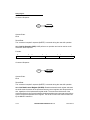
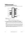
14.4 MOTOROLA RECOMMENDED BDM PINOUT
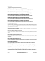
The ColdFire BDM connector is a 26-pin Berg connector arranged 2x13, shown in Figure
14-6.
DEVELOPER RESERVED 2
1
2
BKPT
GND
3
4
DSCLK
GND
5
6
DEVELOPER RESERVED 2
RESET*
7
8
DSI
+5V 1
9
10
DSO
GND
11
12
PST3*
PST2
13
14
PST1
PST0
15
16
DDATA3*
DDATA2
17
18
DDATA1
DDATA0*
19
20
GND
MOTOROLA RESERVED
21
22
MOTOROLA RESERVED
GND
23
24
CLK_CPU
VCC_CPU
25
26
TEA
NOTES:
1 Supplied by target
2 Pins reserved for BDM developer use. Contact developer.
* Denotes a vectored signal
Figure 14-6. 26-Pin Berg Connector Arranged 2x13
14.4.1 Differences Between the ColdFire BDM and a CPU32 BDM
1. DSCLK, BKPT, and DSDI must meet the setup and hold times relative to the rising
edge of the processor clock to prevent the processor from propagating metastable
states.
2. DSO transitions relative to the rising edge of DSCLK only. In the CPU32 BDM, DSO
transitions between serial transfers to indicate to the development system that a command has successfully completed. The ColdFire BDM does not support this feature.
3. The development system must note that the DSO is not valid during the first rising
edge of DSCLK. Instead, the first rising edge of DSCLK causes DSO to transmit the
MSB of DSO. A serial transfer is illustrated in Figure 14-7.
14-38
MCF5206 USERÕS MANUAL Rev 1.0
MOTOROLA
Debug Support
DSCLK
DSI
DSO
16
0
15
16
15
1
0
Figure 14-7. Serial Transfer Illustration
14-39
MCF5206 USERÕS MANUAL Rev 1.0
MOTOROLA
Debug Support
14-40
MCF5206 USERÕS MANUAL Rev 1.0
MOTOROLA