1
TC1775
System Units
Parallel Ports
11.1
General Port Operation
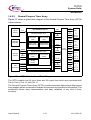
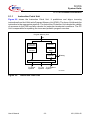
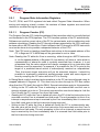
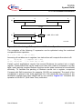
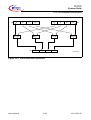
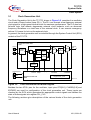
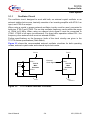
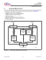
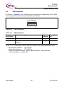
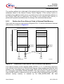
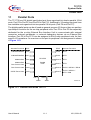
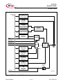
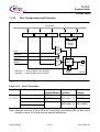
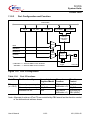
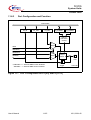
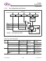
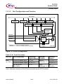
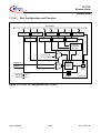
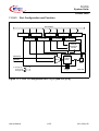
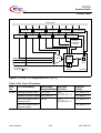
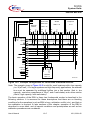
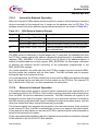
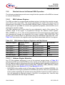
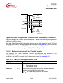
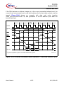
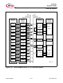
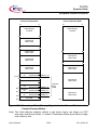
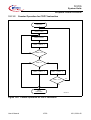
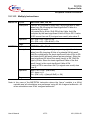
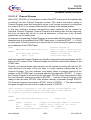
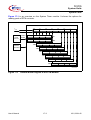
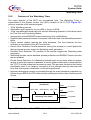
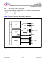
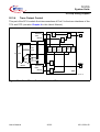
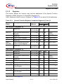
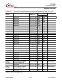
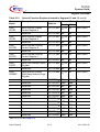
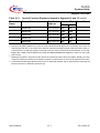
Figure 11-2 shows a general block diagram of an TC1775 port line. Each port line is
equipped with a number of control and data bits, enabling very flexible usage of the line.
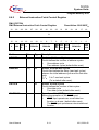
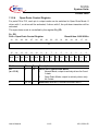
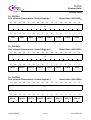
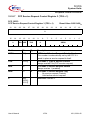
Each port pin can be configured for input or output operation. In input mode (default after
reset), the output driver is switched off (high-impedance). The actual voltage level
present at the port pin is translated into a logic 0 or 1 via a Schmitt-Trigger device and
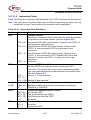
can be read via the read only register Px_IN. In output mode, the output driver is
activated and drives the value supplied through the multiplexer to the port pin. Switching
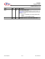
between input and output mode is accomplished through the Px_DIR register, which
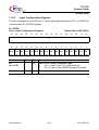
enables or disables the output driver. Alternatively, a peripheral unit can define the port
direction (via AltDir) if it uses bidirectional I/O lines.
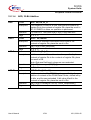
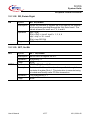
The output multiplexer in front of the output driver enables the port output function to be
used for different purposes. If the pin is used as general purpose output, the multiplexer
is switched by software to the Output Data Register Px_OUT. Software can set or clear
the bit in Px_OUT, and therefore it can directly influence the state of the port pin. If the
on-chip peripheral units use the pin for output signals (line AltEnable active), alternate
output lines can be switched via the multiplexer to the output driver circuitry.
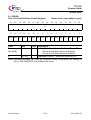
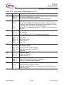
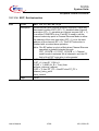
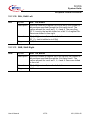
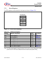
Latch Px_IN is provided for input functions of the on-chip peripheral units. Its input is
connected to the output of the input Schmitt-Trigger. Further, an input signal can be
connected directly to the various inputs of the peripheral units (AltDataIn). The function
of the input line from the pin to the input latch Px_IN and to AltDataIn is independent of
the port pin operates as input or output. This means that when the port is in output mode,
the level of the pin can be read by software via latch Px_IN or a peripheral can use the
pin level as an input. This offers additional advantages in an application.
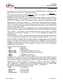
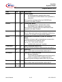
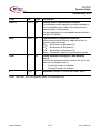
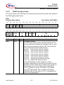
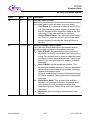
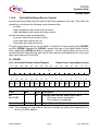
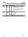
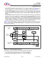
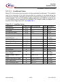
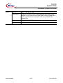
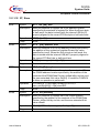
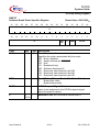
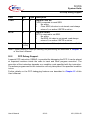
– Each port line can also be programmed to activate an internal weak pull-up or pulldown device. Register Px_PUDSEL selects whether a pull-up or the pull-down
device is activated while register Px_PUDEN enables or disables the pull devices.
– The data written to the output register Px_OUT by software can be used as input
data to an on-chip peripheral. This enables, for example, peripheral tests via
software without external circuitry. Examples for this can be the triggering of a timer
count input, generating an external interrupt, or simulating the incoming serial data
stream to a serial port receive input via software.
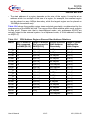
– When the pin is used as an output, the actual logic level at the pin can be examined
through reading latch Px_IN and compared against the applied output level (either
applied through software via the output register Px_OUT, or via an alternate output
function of a peripheral). This can be used to detect some electrical failures at the
pin caused through external circuitry. In addition, software supported arbitration
schemes can be implemented in this way using the open-drain configuration and
an external wired-And circuitry. Collisions on the external communication lines can
be detected when a logic 1 is output, but a logic 0 is seen when reading the pin
value via the input latch Px_IN.
User’s Manual
11-2
V2.0, 2001-02