1
TC1775
System Units
Memory Protection System
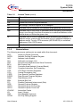
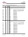
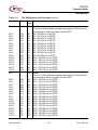
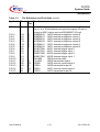
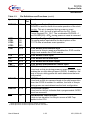
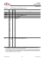
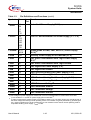
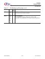
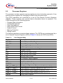
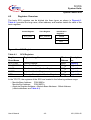
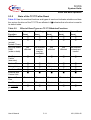
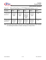
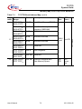
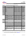
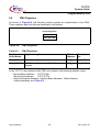
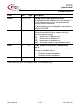
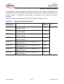
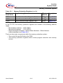
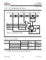
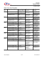
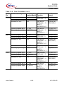
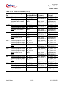
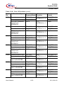
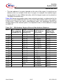
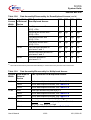
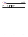
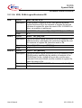
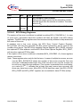
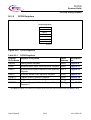
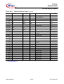
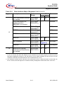
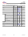
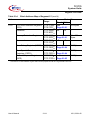
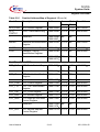
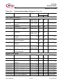
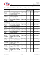
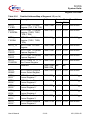
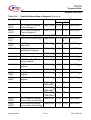
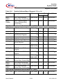
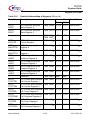
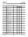
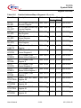
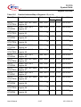
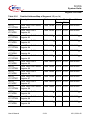
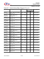
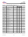
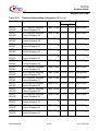
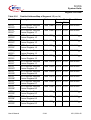
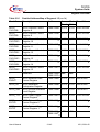
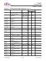
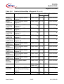
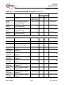
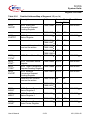
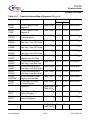
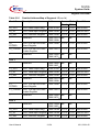
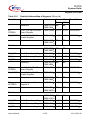
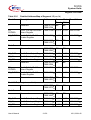
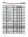
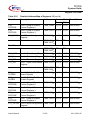
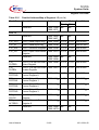
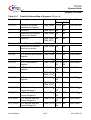
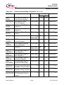
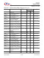
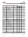
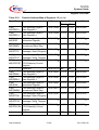
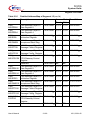
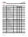
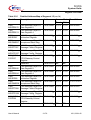
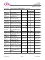
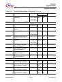
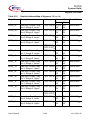
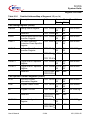
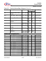
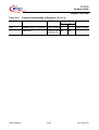
Table 10-1
Memory Protection Registers (cont’d)
Register
Short Name
Register Long Name
Offset
Address
Description
see
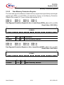
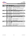
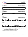
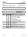
DPM1
Data Protection Mode Register, Set 1
2080H
Page 10-12
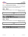
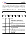
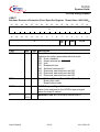
CPM0
Code Protection Mode Register, Set 0
2200H
Page 10-15
CPM1
Code Protection Mode Register, Set 1
2280H
Page 10-15
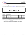
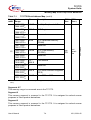
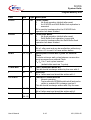
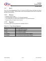
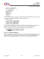
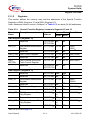
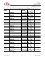
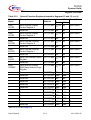
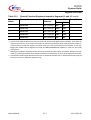
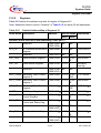
In the TC1775, the memory protection registers are located in the following address
range:
– Module Base Address. FFFF C000H
Module End Address. FFFF EFFFH
– Absolute Register Address = Module Base Address + Offset Address
(offset addresses see Table 10-1)
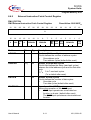
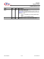
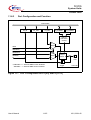
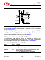
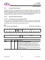
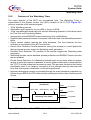
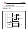
There are two major components within the memory protection system:
– The control bits and bit fields in the PSW.
– The memory protection registers which control program execution and memory
access.
User’s Manual
10-6
V2.0, 2001-02