1
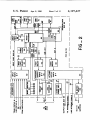
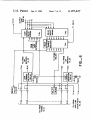
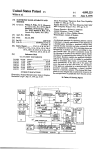
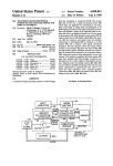
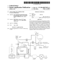
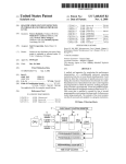
9
4, 197,427
microprocessor 60. OUT 1 strobes information into
eight latching output ports, having a plurality of output
lines per port and OUT 2 strobes information into the
eight non-latching ports with each port having onlme
line. The final signal is the WRITE ENABLE (WE)
signal. This signal tells the RAM 76 whether the micro
processor wishes to read data out of or load data into
the RAM 76. A detailed understanding of how the
above-described signals are produced by the state de
coder 212 is not necessary to appreciate the present
10
is addressed, except instead of using just the address
register 80, the ROM 74 additionally uses a ROM chip
select register 78. The addressing scheme for both the
ROM 74 and RAM 76 memories is set up so that every
memory location, whether it be in the ROM 74 or the
RAM 76, is uniquely addressable by the microprocessor
60.
The ROM 74 contains all the stored programs for the
line concentrator 8. Details of this control cycle pro
gram will be discussed in the System Operation section
invention. Reference to the INTEL 8008 User’s Manual
is suggested if further information on the speci?c con
below. In the present embodiment, the ROM 74 has a
capacity of over 14,000 words. It is further designed to
trol circuitry necessary to provide the described signal
operations is desired.
enable expansion of memory capacity when needed.
(2) The RAM Subsystem
A typical random access memory (RAM) and mem
ory addressing scheme is shown in the system block
diagram of FIG. 2. In the present embodiment, the
RAM 76 has a storage capacity of 2048 eight-bit words.
Memory addresses from the microprocessor 60 are cou
pled by the processor bus 90 to a sixteen-bit address
Stored in the ROM 74 is the concentrator 8 system
15 control program for use by and control of the micro
processor 60. The advantages of ROM controlled sys
tems is that once data or instructions are stored in the
ROM, the information cannot be affected by system
power failure or processor re-programming, whereas
information in a RAM is alterable in these ways. Note
that ROM’s can be initially programmed only by special
devices at the factory, and although some ROM’s have
the capability of being re-programmed, this also can
register 80. Control signals CLR, Eli, and E'r? from
only be accomplished by special devices which are not
the microprocessor 60, strobe an address into the ad
dress register 80 as two eight-bit bytes to create the 25 a part of the present invention.
The ROM 74, if addressed by the microprocessor 60,
sixteen-bit address word. In the present embodiment,
outputs data onto the same memory bus 92 as does the
only 12 of these sixteen address bits are used in address
RAM 76. This data is coupled to the processor 60 via
ing the RAM 76. The address register 80 is required to
the input data multiplexer 88 and processor bus 90. The
retain the address desired, since the processor bus 90 is
also used in a later part of the microprocessor 60 mem 30 addressing scheme for the ROM 74 is slightly different
from that of the RAM 76, in that the address register 80
ory cycle as a data bus, wherein data is either received
only feeds the ?rst eight bits of address directly to the
by the microprocessor 60 or sent out from it to be stored
ROM 76 for word selection, while four additional ad
in the RAM 76.
dress bits (e.g. A8-All) are coupled to the ROM chip
During a read cycle, the RAM 76 outputs data to the
microprocessor 60 on the memory data bus 92. During 35 select register 78. In the present embodiment, the regis
ter 78 comprises a plurality of chip select registers, one
such a read cycle, the data is coupled to the micro
each on each memory board containing ROM chips.
processor 60 from the memory data bus 92 through an
The register 78 functions to selectively enable the ad
input multiplexer 88, which is used to give the micro
dressing of a given ROM chip based on the state of
processor 60 the choice of inputting either RAM 76 or
ROM 74 memory information or data from one of the 40 address bits A8-A13. Each ROM chip presently con
tains 256 eight-bit words, so that address bits A¢—A7
input ports 62. The output from the input multiplexer 88
are used to select a specific word location on the ROM
is coupled to the microprocessor 60 by the bidirectional
chip selected by the register 78. It is within the scope of
processor bus 90. Data is inputted to the RAM 76 for
the present invention to incorporate ROM’s of higher
storage directly from the microprocessor 60 by means
of the processor bus 90. As mentioned above, the RAM 45 bit density as they become available, e.g. ROMs having
2024 eight-bit words.
76 is told whether or not the microprocessor 60 wishes
to write data into the RAM 76 or read data from the
RAM 76 by means of the WRITE ENABLE (W—E) line,
as illustrated in FIGS. 2 and 3. When information is to
be read from the RAM 76 to the micgprocessor 60,
only the address need be given, the WE line is not
strobed. Writing informatirmnto the RAM 76, how
ever, does require that the WE line be strobed.
As shown in FIG. 4, the RAM 76 is organized into
(4) Input/Output Devices
As shown in FIG. 2, there are eight latchable regis
ters of eight bits each that comprise the output ports 66,
and eight strobing output ports 70 of one bit each. These
output ports 66, 70 communicate control functions and
data to the respective devices, corresponding to a given
port, that the microprocessor 60 wishes to access. The
different sub-blocks, including blocks of storage space 55 ports 66, 70 connect to subsystems both within the PCC
12, 22 and external to it. The means for choosing which
for trunk and switching matrix status, a scratch pad for
port passes information to its respective subsystem com
temporary storage of numbers being operated on, a
prises two output port select units 68, 72. The port
queue for the storage of detected service requests that
select 68 selects one of the eight latching output ports 66
have not yet been switched through, and various pro
for information transfer, and the port select 72 selects
gram pointers for enabling the microprocessor 60 to
one of the eight strobing ports 70 for information trans
return to routines that have been temporarily stopped in
fer. Each port select unit 66, 72 decodes three input
order to perform routines of higher priority.
lines (A9-All) from the address/data bus 92 into eight
(3) The ROM Subsystem
output lines for individual selection of one of the eight
A typical, non-destructive, read only memory 65 output ports. The OUT 1 and OUT 2 signals, originat
ing from the microprocessor 60 also input to the port
(ROM) 74 and memory addressing scheme is also
select units. Signal OUT 1 enables operation of port
shown in the system block diagram of FIG. 2. The
select 68, and signal OUT 2 enables operation of port
ROM 74 is addressed in the same way that the RAM 76