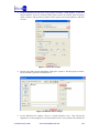
1
iCEcube2 User Guide v1.4 – September 2011 Copyright Information Copyright © 2008-2011 SiliconBlue Technologies Corporation. All rights reserved. SiliconBlue is a trademark of SiliconBlue Technologies Corporation. Magma and Blast FPGA are trademarks Magma Design Automation, Inc. Synopsys and Synplify Pro are trademarks of Synopsys, Inc. All other trademarks are the property of their prospective owners. All specifications are subject to change without notice. Notice of Disclaimer: This software is provided to you "as-is," without any express or implied warranty. Contact Information SiliconBlue Technologies Corporation 3255-7 Scott Blvd., Suite 101 Santa Clara, CA 95054 Tel: (408) 727-6101 Fax: (408) 727-6085 [email protected] Revision History The following table lists the revision history of this document. Version Revision 1.0 Release iCEcube2 2010.03 1.1 Release iCEcube2 2010.09 1.2 Release iCEcube2 2010.12 1.3 Release iCEcube2 2011.06 1.4 Release iCEcube2 2011.09 iCEcube2 User Guide www.SiliconBlueTech.com 2 TABLE OF CONTENTS Preface ........................................................................................................... 5 About this Document ............................................................................................................................. 5 Software Version ..................................................................................................................................... 5 Platform Requirements .......................................................................................................................... 5 Programming Hardware ....................................................................................................................... 5 Chapter 1 Overview .................................................................................... 6 iCEcube2 Tool Suite ................................................................................................................................ 6 Design Flow ............................................................................................................................................. 7 Chapter 2 Quick Start Guide .................................................................... 8 Creating a Project .................................................................................................................................... 8 Synthesizing the design ........................................................................................................................12 Programming the Device ......................................................................................................................27 Addendum:.............................................................................................................................................28 Importing Physical Constraints from iCEcube to iCEcube2 .......................................................28 Chapter 3 iCEcube2 Project Setup and Navigation ........................... 32 Introduction ............................................................................................................................................32 Project Manager GUI .............................................................................................................................33 Adding/Deleting Design and Constraint Files .................................................................................33 Selecting the Target Device and Operating Conditions ...................................................................35 Output Window .....................................................................................................................................37 PLL Module Generator .........................................................................................................................37 Chapter 4 iCEcube2 Physical Implementation Tools ........................ 47 Overview .................................................................................................................................................47 Tools for Physical Implementation ......................................................................................................47 Placing and Routing the Design ..........................................................................................................48 Floor Planner ..........................................................................................................................................49 Package View .........................................................................................................................................56 Pin Constraints Editor ...........................................................................................................................58 Power Estimator .....................................................................................................................................59 Generating a Bitmap ..............................................................................................................................61 Programming the Device ......................................................................................................................62 Simulating the Routed Design .............................................................................................................66 Chapter 5 Timing Constraints and Static Timing Analysis ............. 68 Overview .................................................................................................................................................68 Specifying Constraints Using the Timing Constraints Editor (TCE) ..............................................68 SDC Constraints in TCE ...................................................................................................................70 Clock Constraints ..............................................................................................................................70 Generated Clock Constraints ...........................................................................................................70 Source Clock Latency Constraints ..................................................................................................71 Input Delay Constraints ...................................................................................................................71 Output Delay Constraints ................................................................................................................72 Max Delay Constraints .....................................................................................................................72 False Path Exceptions .......................................................................................................................73 Multi Cycle Path Exceptions ............................................................................................................74 3 www.SiliconBlueTech.com iCEcube2 User Guide Analyzing Reports Generated by the Static Timing Analyzer (STA) .............................................75 Clock Summary Pane .......................................................................................................................75 Clock Relationship Summary ..........................................................................................................79 Data Sheet ..........................................................................................................................................79 Analyzing Constrained Paths ..........................................................................................................81 By Slack ............................................................................................................................................81 By Paths ............................................................................................................................................83 Point to Point ...................................................................................................................................85 Other Features ...................................................................................................................................87 Detailed Timing Report ........................................................................................................................89 Chapter 6 Physical Constraints in iCEcube2 ....................................... 94 Specifying Physical Constraints after Design Import and Before Placement ................................94 Absolute Placement ..........................................................................................................................94 Constraining Logic or RAMs ........................................................................................................94 Constraining IOs .............................................................................................................................95 Relative Placement ............................................................................................................................95 IO/FF Merge ....................................................................................................................................100 Global Buffer Promotion/Demotion ............................................................................................102 Modifying the Device Floor Plan after Placement ..........................................................................104 Chapter 7 Generating/Integrating Fixed Placement IP Blocks ...... 107 IP Generation Flow ..............................................................................................................................107 System Design Flow ............................................................................................................................110 Appendix A: PCF Syntax ....................................................................... 115 iCEcube2 User Guide www.SiliconBlueTech.com 4 Preface About this Document The iCEcube2 User Guide provides iCE FPGA designers with an overview of the software tools and the design process using iCEcube2. This document covers the iCEcube2 tools for Project Setup, Navigation, and Physical Implementation on the iCE FGPA device. For information on the Synopsys Synplify Pro software, please refer to the Synplify Pro documentation provided in the synpro/doc directory in the iCEcube2 software installation (<icecube2_install_dir>/synpro/doc), and on the SiliconBlue website. Software Version This User Guide documents the features of iCEcube2 Software Version 2011.09 For more information about acquiring the iCEcube2 software, please visit the SiliconBlue website: http://www.siliconbluetech.com. Platform Requirements The iCEcube2 software can be installed on a platform satisfying the following minimum requirements. A Pentium 4 computer (500 MHz) with 256 MB of RAM, 256MB of Virtual Memory, and running one of the following Operating Systems : Windows 7 OS, 32-bit / 64-bit Windows XP Professional Red Hat Enterprise Linux WS v4.0 Programming Hardware There are three ways to program iCE FPGA devices: 5 A third party programmer, using the programming files generated by the iCEcube2 Physical Implementation Tools. Consult the third party programmer user manual for instructions. The iCEman Evaluation Board, which not only serves as a vehicle to evaluate iCE FPGAs, but also includes an integrated device programmer. This programmer can be used to program devices on the iCEman board, or it can be used to program devices in a target system. Please contact SiliconBlue Technologies for additional information on the iCEman Evaluation Board. Digilent USB cables www.SiliconBlueTech.com iCEcube2 User Guide Chapter 1 Overview iCEcube2 Tool Suite The iCEcube2 Tool Suite is comprised of several integrated components, running under either the Microsoft Windows or the Red Hat Linux environments. Please refer to Platform Requirements for additional information on supported operating systems. The figure below depicts the design flow using the iCEcube2 Tool Suite. The components in blue signify functionality supported by SiliconBlue Technologies‟ proprietary iCEcube2 software, and the components in purple indicate the functionality supported by Synopsys‟ Synplify Pro synthesis tools. The iCEcube2 software and Synopsys software together constitute the iCEcube2 Tool Suite. Figure 1-1: The iCEcube2 Design Flow iCEcube2 User Guide www.SiliconBlueTech.com 6 Design Flow The following steps provide an overview of the design flow using the iCEcube2 Tool Suite. 1. Create a new project in the iCEcube2 Project Navigator and specify a target device and its operating conditions. Add your HDL (Verilog or VHDL) design files and your Constraint files to the project. 2. Synthesize your design using the Synplify Pro design software. This software has been provided as part of the iCEcube2 Tool Suite, and can be invoked from the iCEcube2 Project Navigator. Within the Synopsys design environment, assign your Logic Synthesis, Timing and Pin constraints. 3. Perform Placement and Routing using the iCEcube2 place and route tools. iCEcube2 also supports physical implementation tools such as floor planning, allowing users to manually place logic cells and IOs. 4. Perform timing simulation of your design using an industry-standard HDL simulation tool. The files necessary for simulation are automatically generated by the iCEcube2 Physical Implementation tools, after the routing phase. 5. Perform Static Timing Analysis using the iCEcube2 static timing analyzer. 6. Generate the device programming and configuration files from the iCEcube2 Physical Implementation tools. 7. Program your device using the device programming hardware provided by Silicon Blue Technologies. 7 www.SiliconBlueTech.com iCEcube2 User Guide Chapter 2 Quick Start Guide This chapter provides a brief introduction to the iCEcube2 design flow. The goal of this chapter is to familiarize the user with the fundamental steps needed to create a design project, synthesize and implement the design, generate the necessary device configuration files, and program the target device. Detailed information on tool features and usage is provided in subsequent chapters. Creating a Project Starting the iCEcube2 software for the first time, you will see the following interface shown in Figure 2-1. Figure 2-1 : Create a New Project The first step is to create a new design project and add the appropriate design files to your project. You can create a new project by either selecting File>New Project from the iCEcube2 menu, or by clicking the Create a New Project icon as seen in Figure 2-1. The New Project Wizard GUI is displayed in Figure 2-2. iCEcube2 User Guide www.SiliconBlueTech.com 8 Figure 2-2 : New Project Setup Wizard for iCE40 Family This example is targeted for iCE65 family device. Follow the following steps to setup the project properties. 1. Project Name Field: Specify a project name (quick_start) in the Project Name field. 2. Project Directory Field: Specify any directory where you want to place the project directory in the Project Directory field. 3. Device Family Fields: This section allows you to specify the SiliconBlue device family you are targeting. For this example, change the Device Family to iCE65. 4. Device Fields: This section allows you to specify the SiliconBlue device and package you are targeting. For this example, change the Device to L04 and change the device package to the CB284. For iCE65 family the user has to set the device Power Grade. Set Power Grade to L. 9 www.SiliconBlueTech.com iCEcube2 User Guide 5. Operating Condition Fields: This section allows you to specify the operating conditions of the device which will be used for timing and power analysis. The IO Bank Voltage option shown in Figure 2-2 is not available for iCE65 family devices. 6. Start From Synthesis: This option allows you to start the flow from Synthesis using Synopsys Synplify Pro tool. For current example, select this option. 7. Start From BackEnd: This option allows the user to start from Post Synthesis flow. After the above selections the New Project GUI Wizard has the following settings. ` iCEcube2 User Guide www.SiliconBlueTech.com 10 8. Click Next to go to the Add Files dialog box shown in Figure 2-3. You will be prompted to create a new project directory. Click Yes. 9. In the Add Files dialog box, navigate to: <iCEcube2 installation directory>/examples/blinky Highlight the following files: blinky.vhd blinky_syn.sdc* Select each file and click >> to add the selected file, or click >>> to add all the files in the open directory (files can be removed using << and <<<) to your project. Click Finish to create the project. * The SDC file is a Synopsys constraint file, which contains timing constraint information. Figure 2-3: New Project Wizard – Add Files dialog box After successfully setting-up your project, you will return to the following iCEcube2 Project Navigator screen shown in Figure 2-4. 11 www.SiliconBlueTech.com iCEcube2 User Guide Figure 2-4: iCEcube2 Project Navigator View after Completing Project Set-up Synthesizing the design After a successful project setup, Double-Click on the Launch Synthesis Tool icon in the project navigator window. See Figure 2-5. This will bring-up the Synopsys Synplify Pro synthesis tool‟s graphical user interface. See Figure 2-6. iCEcube2 User Guide www.SiliconBlueTech.com 12 Figure 2-5 : Launch Synthesis Tool 13 www.SiliconBlueTech.com iCEcube2 User Guide Figure 2-6 : Synplify Pro Graphical User Interface Hit the Run Button to synthesis your design. Once synthesis is complete, you will see a Done message. See Figure 2-7. iCEcube2 User Guide www.SiliconBlueTech.com 14 Figure 2-7 : Status showing synthesis has been completed View Timing Constraints Double Click on the blinky_syn.sdc file under the Constraint folder. See Figure 2-8. It will open the timing constraints for the project shown in Figure 2-9. 15 www.SiliconBlueTech.com iCEcube2 User Guide Figure 2-8 : Open the SDC file to View Timing Constraints iCEcube2 User Guide www.SiliconBlueTech.com 16 Figure 2-9 : View Timing Constraints Viewing Hierarchical View of Synthesis Results Under the HDL-Analyst menu, Select RTL > Hierarchical View. You will see a hierarchical RTL view of the design just synthesized. See Figure 2-10. 17 www.SiliconBlueTech.com iCEcube2 User Guide Figure 2-10 : Hierarchical RTL View in HDL Analyst If you double click on one of the blocks, it will take you to the RTL for that block. See Figure 2-11. iCEcube2 User Guide www.SiliconBlueTech.com 18 Figure 2-11 : Double-clicking on a block will reveal its HDL code in HDL Analyst Select Implementation In order to ensure that the synthesized design can be successfully imported into iCEcube2, exit the Synplify Pro GUI. Return to the iCEcube2 Navigator and Double-click on Select Implementation. See Figure 2-12. This will tell iCEcube2 which synthesis implementation to process for place and route. If you have different synthesis implementations, you will be able to select the synthesis implementation you wish to place and route. Since we only have one implementation, select OK when the Select Synthesis Implementation dialog box appears. 19 www.SiliconBlueTech.com iCEcube2 User Guide Figure 2-12 : Select Synthesis Implementation Importing Physical Constraints Physical constraints such as pin assignments are stored in a .PCF file (Physical Constraint File). Add the .PCF file to your project. In the iCEcube2 Project Navigator, Right Click on Constraint Files. Select Add Files… See Figure 2-13. Note: For information on importing physical constraints from iCEcube to iCEcube2, please refer to the Importing Physical Constraints from iCEcube to iCEcube2 section at the end of this quick start guide. iCEcube2 User Guide www.SiliconBlueTech.com 20 Figure 2-13 : Specify Additional Files for Place and Route Navigate to the <iCEcube2 Installation Directory>/examples/blinky and Add blinky.pcf file. See Figure 2-14. Figure 2-14 : Add .pcf file Import Place & Route Input Files 21 www.SiliconBlueTech.com iCEcube2 User Guide The next step is to import the files for Place and Route. Double-click on Import P&R Input Files in the Project Navigator. See Figure 2-15. Once completed you will see a green check next to Import P&R Input Files. See Figure 2-16. Figure 2-15 : Import P&R Input files Figure 2-16: Successful Import of P&R Input Files iCEcube2 User Guide www.SiliconBlueTech.com 22 Place the Design Double-click on Run Placer Once placement is complete, a green check will appear and the Output window will show information about the placement of the design. See Figure 2-17. Figure 2-17 : Place complete View Floorplanner At this point, since placement has been completed, you can view the placement of the design by opening the Floorplanner. You can open the Floorplanner by going to the menu and selecting Tool > Floorplanner or you can also select the Floorplanner Icon. See Figure 2-18. 23 www.SiliconBlueTech.com iCEcube2 User Guide Figure 2-18 – Floorplanner View the Package Viewer You can also see how pins were placed for your design by selecting the Package Viewer. You can select the package viewer by going to the menu and selecting Tool >> Package Viewer or you can also select the Package Vierwer Icon. See Figure 2-19. iCEcube2 User Guide www.SiliconBlueTech.com 24 Figure 2-19 : Package Viewer Route the Design Double-click on Route in the project navigation window. Place and Route have been separated into different steps as to allow you to re-route the design after making placement modifications in the floorplanner without having to re-run the placer. 25 www.SiliconBlueTech.com iCEcube2 User Guide Perform Static Timing Analysis Now that you have routed the design, you can perform timing analysis to check to see if the design is meets your timing requirements. To launch the timing analyzer, go to the menu and select Tool > Timing Analysis. You can also select the Timing Analysis Icon. See Figure 2-22. Figure 2-22 : Timing Analysis Summary You can see from the timing analysis that our 1MHz design is running at over 117 MHz and our 32 MHz clock is running at over 79 MHz (worst case timing). If we were not meeting timing, the timing analyzer will allow you to see your failing paths and do a more in-depth analysis. For this tutorial, we won‟t go into details on timing slack analysis. Perform Power Analysis iCEcube2 also comes with power estimator tool. To launch the power estimator, to the menu and select Tool >> Power Estimator. You can alternatively select the power estimator icon. Figure 2-23. There are multiple tabs in the Power Estimator tool including Summary, IO, and Clock Domain. On the Summary tab, change the Core Vdd to 1.0V and make sure all IO voltages are at 2.5V. Then hit calculate. The estimator will update with power information for both static and dynamic power. For more information on using the IO and Clock Domain tabs, please refer to the detailed section on the Power Estimator tool. iCEcube2 User Guide www.SiliconBlueTech.com 26 Figure 2-23 : Power Estimator Programming the Device In order to program a device, you will need to generate a programming file. In the project navigator, double click on Bitmap. You are now ready to program an iCE65 mobileFPGA deice with the generated bitmap. Invoke the programmer from the Programming icon which is now enabled in the Project Navigator. Alternately, you may invoke it from the Tool>Programmer menu item. The iCEman65 Evaluation Kit Board includes an on-board USB 2.0 programming solution to program the on-board SPI serial Flash or the iCE65 device directly. In a future iCEcube2 release, the utility will also support direct programming of the iCE65 device, although this is not currently supported. Additional details on programming a device are provided in a separate section Programming the Device in the chapter on iCEcube2 Physical Implementation Tools. 27 www.SiliconBlueTech.com iCEcube2 User Guide 2-24 : Programmer Graphical User Interface Addendum: Importing Physical Constraints from iCEcube to iCEcube2 For users who have created physical constraints using iCEcube, this section describes how to import and convert those constraints for use in iCEcube2. This section will demonstrate how to import a .MTCL file from iCEcube and save it into .PCF format used in iCEcube2. In the iCEcube2 project navigator, Right-click on Specify Additional Files. See Figure 2-25 iCEcube2 User Guide www.SiliconBlueTech.com 28 Figure 2-25 : Add additional constraint file Navigate to the <iCEcube2 Installation Directory>/examples/blinky and Add blinky.mtcl file. See Figure 2-26. Figure 2-26 : Add .mtcl file Import Place & Route Input Files 29 www.SiliconBlueTech.com iCEcube2 User Guide The next step is to import the files for Place and Route. Double-click on Import P&R Input Files in the Project Navigator. See Figure 2-27. Once completed you will see a green check next to Import P&R Input Files. See Figure 2-28. Figure 2-27 : Double-click on Import P&R Input files iCEcube2 User Guide www.SiliconBlueTech.com 30 Figure 2-28: Successful Import of P&R Input Files Saving Physical Constraints into .pcf Format Open the Pin Constraints Editor by going to the menu and selecting Tool>Pin Constraints Editor or you can also select the Pin Constraints Editor Icon. See Figure 2-29. You will se a list of pin assignments that are Locked under the locked column. Uncheck and Recheck one of the pins under the locked column. The save icon will now become an active icon. Click on the Save physical constraints icon. This will bring up a dialog box where you can save the PCF file. Hit OK. See Figure 2-30. The .PCF file contain physical constraints in the design used for place and route. 31 www.SiliconBlueTech.com iCEcube2 User Guide Figure 2-29 : Pin Constraints Editor. Figure 2-30 : Pin Constraints Editor. Chapter 3 iCEcube2 Project Setup and Navigation Introduction This chapter describes the features of the iCEcube2 Project Manager and how to set up a design Project. The primary functions of the Project Manager include project setup, launching the Synopsys Synplify Pro tools for synthesis, placing and routing the design, and launching the software required to Program the target device. iCEcube2 User Guide www.SiliconBlueTech.com 32 This chapter assumes that the reader is familiar with the New Project creation process as described in Chapter 2 Quick Start. Project Manager GUI Figure 3-1 below displays the Project Manager GUI. A new project can be opened by clicking on the New Project icon or the File>New Project menu item as displayed in Figure 3-1 : iCEcube2 Project Flow Manager. Similarly, an existing project can be opened or closed using the Open Project and Close Project icons. Figure 3-1 : iCEcube2 Project Flow Manager Adding/Deleting Design and Constraint Files Design and Constraint files can be added/removed from the project by selecting Design Files or Constraint Files respectively as displayed in Figure 3-2. 33 www.SiliconBlueTech.com iCEcube2 User Guide Figure 3-2 : Adding/Removing Design Files to the design project Deleting a specific file can be accomplished by selecting the file name and clicking the rightbutton on the mouse. Figure 3-3 below displays the state of the GUI upon clicking the mouse button. iCEcube2 User Guide www.SiliconBlueTech.com 34 Figure 3-3 : Removing Files from the design project Selecting the Target Device and Operating Conditions The iCEcube2 software provides the ability to specify the operating conditions for the target device. In order to change the Target Family, Device and/or the Operating Conditions, click the right-button on the mouse, in the Device/Operating Condition window to display the Edit action. This is shown in Figure 3-4. Figure 3-4 : Modifying the Device Selection/Operating Conditions The following Figures 3-5 and 3-6 displays the Device Options Wizard based on the selected device family. 35 www.SiliconBlueTech.com iCEcube2 User Guide Figure 3-5: Device Options Wizard for iCE40 Family Figure 3-6 : Device Options Wizard for iCE65 Family iCEcube2 User Guide www.SiliconBlueTech.com 36 In order to specify a suitable target Device, the following steps need to be performed: 1. Specify a Device Family 2. Specify a Device using the drop-down menu 3. Select a suitable Device Package for the device selected in the previous step 4. Specify a Power Grade for the selected device. This option is available only for iCE65 family as shown in Figure 3-6. The iCEcube2 software supports two Power Grades, viz. the “-L” which signifies the Low Power device and the “–U” which signifies the Ultra-Low-Power device. Specifying the Operating Conditions for the target device involves the following steps: 1. Junction Temperature a. Select an appropriate Junction Temperature Range from the options available. Depending on the Power Grade selected for the target device, the software provides built-in options such as Commercial and Industrial temperature ranges. b. If the device‟s operating conditions do not fall into either the Commercial or the Industrial temperature ranges, the software also permits the user to specify a customized junction temperature. This is accomplished by selecting the Custom option, and manually specifying the Best, Typical and Worst Case junction temperatures. 2. Core Voltage : Select a Voltage Tolerance Range from the provided options. 3. IOBank Voltage: This option is available only for iCE40 family as shown in Figure 3-5. Select a bank voltage from the provided options for the top, bottom, left, right banks. The specified IO Voltage values are used by Power Estimator and Static Timing Analysis tools. In order for Static Timing Analysis to be performed at the desired Operating Conditions, the software provides the ability to select the Best Case, Typical Case or Worst Case conditions. Output Window The iCEcube2 Project Flow Manager software provides an Output Window to display messages, warnings and errors. PLL Module Generator Certain devices of the iCE65, iCE40 family include a Phase Lock Loop (PLL) function. The PLL function requires configuration before it can be used in a design. To help configure the PLL, the iCEcube2 Project Flow Manager includes a PLL Module Generator, which can be launched from the Tool>Configure PLL Module menu item, as displayed in Figure 3-6. 37 www.SiliconBlueTech.com iCEcube2 User Guide Figure 3-5: Launching the PLL Module Generator The PLL Module Generator allows the user to create a new PLL configuration, or edit an existing one as shown in Figure 3-7. The output of the PLL Module Generator is a PLL module file (Verilog), that instantiates a PLL, as configured by the user. A secondary file (wrapper), that includes an instance of the PLL module, is generated in order to help instantiate the PLL module in the user‟s design. Note that the PLL module file should be included in the list of design files. Once a PLL module file has been generated, it can be edited, by selecting the “Modify an existing PLL configuration” option (Figure 3-7). iCEcube2 User Guide www.SiliconBlueTech.com 38 Figure 3-6: Create/Modify a PLL configuration Configuring a iCE65 PLL Module In the PLL Module Generator wizard select Device Family as iCE65 and provide the PLL Module Name. Click on the OK button. The PLL Module Generator launches a wizard to help the user configure the PLL as per the design requirements. This section describes the features of iCE65 family PLL modules. PLL Type The connectivity of the PLL to its surrounding logic determines the PLL Type. The iCEcube2 software supports the following PLL types. These PLL type options can be selected on the first page of the wizard, as displayed in Figure 3-9. 39 1. General Purpose IO Pad or Core Logic: In this scenario, the PLL input (source clock) is driven by a signal from the FPGA fabric. This signal can either be generated on the FPGA core, or it can be an external signal that was brought onto the FPGA using a General Purpose IO pad. The PLL output (generated clock) is available on the FPGA to drive a global clock network, as well as regular routing. 2. Clock Pad: The PLL input clock (source) is driven by a dedicated clock pad located in IO Bank 2 a. The PLL output (generated clock) is available to drive a global clock network, as well as regular routing. The PLL source clock is not available on the FPGA. b. The PLL output (generated clock) is available to drive a global clock network, as well a regular routing. The PLL source clock is also available on the FPGA, and can drive a global clock network, as well as regular routing. www.SiliconBlueTech.com iCEcube2 User Guide Figure 3-7: Selecting the PLL Type and Operation Mode PLL Operation Modes The PLL can be configured to operate in one of multiple modes. An Operation Mode determines the feedback path of the PLL, and enables phase alignment of the generated clock w.r.t. to the source clock. The iCEcube2 software supports the following PLL Operation modes: 1. No Compensation mode: The PLL can be used for generating the desired output frequency, without the ability to control the phase of the generated clock. 2. Delay Compensation using only the Fine Delay Adjustment (FDA) Block: In this mode, the feedback path is internal to the PLL but traverses through a fine delay adjustment circuit that permits user control of the feedback path delay in 16 steps of 0.15 ns each. The delay adjustment can be controlled dynamically through signals connected to the PLL, or iCEcube2 User Guide www.SiliconBlueTech.com 40 it can be fixed i.e. once configured, the delay contributed by the delay block can only be changed upon re-programming the FPGA with a different bit configuration. 3. Delay Compensation using the Phase Shifter and the Fine Delay Adjustment (FDA) Block. The Phase Shifter provides 4 outputs corresponding to a phase shift of 0 degrees, 90 degrees, 180 degrees or 270 degrees. In addition, this feedback path provides additional delay adjustment through the FDA block. 4. Delay Compensation using a feedback path external to the PLL: The feedback path traverses through FPGA routing (external to the PLL) followed by the Fine Delay Adjustment (FDA) Block. Hence, in effect, 2 delay controls are available – the external path for coarse adjustment and the FDA block for fine delay adjustment. Figure 3-8 : PLL Module Generator – Frequency Specification Fine Delay Adjustment: The delay contributed by the FDA block can be Fixed or controlled dynamically during FPGA operation. If Fixed, it is necessary to provide a number (n) in the range 41 www.SiliconBlueTech.com iCEcube2 User Guide 0-15 to specify the delay contributed to the feedback path. The delay for a setting “n” is calculated as follows FDA delay = (n+1)*0.15 ps, where “n” is the value specified by the user, and 0 ≤ n ≤ 15 Frequency Specification: The input and output frequency of the PLL should be specified in MHz as shown in Figure 3-10. Depending on the values provided by the user, the PLL is internally configured to generate the specified output frequency. Frequency Specification window also checks for the input and output frequencies given by the user. If the specified frequencies are at a range that cannot be generated by the PLL, then a popup comes out as shown in Figure 3-91 asking the user to enter the frequencies in valid range. Figure 3-9: Frequency Validation by PLL Configurator Other options: LOCK: A Lock signal is provided to indicate that the PLL has locked on to the incoming signal. Lock asserts High to indicate that the PLL has achieved frequency lock with a good phase lock. BYPASS: A BYPASS signal is provided which both powers-down the PLL core and bypasses it such that the PLL output tracks the input reference frequency. Low Power Mode: A control is provided to dynamically put the PLL into a Lower Power Mode through the iCEGate feature. The iCEGate feature latches the PLL Output signal, and prevents unnecessary toggling. The RESET (Active Low) port is always generated, so that an explicit PLL reset or bypass operation is required to initialize the PLL functionality. iCEcube2 User Guide www.SiliconBlueTech.com 42 Configuring a iCE40 PLL Module In the PLL Module Generator wizard select Device Family as iCE40 and provide the PLL Module Name. Click on the OK button. The PLL Module Generator launches a wizard to help the user configure the PLL as per the design requirements. This section describes the features of iCE40 family PLL modules. PLL Type The connectivity of the PLL to its surrounding logic determines the PLL Type. The iCEcube2 software supports the following PLL types. These PLL type options can be selected on the first page of the wizard, as displayed in 3-12. 43 1. Select the number of global networks to be driven by the PLL output. Setting the value to “1” generates a PLL which drives a single global clock network, as well as regular routing. Setting the value to “2” generates a PLL which drives two global clock networks as well as two regular routing resources. 2. Select one of the following 2 options : a. General Purpose IO Pad or Core Logic: In this scenario, the PLL input (source clock) is driven by a signal from the FPGA fabric. This signal can either be generated on the FPGA core, or it can be an external signal that was brought onto the FPGA using a General Purpose IO pad. b. Clock Pad: The PLL input clock (source) is driven by a dedicated clock pad located in IO Bank 2 (Bottom bank) or IO Bank 0 (Top bank). If the number of global networks is“2”, the source clock of the PLL can be used as is, i.e. without any frequency, delay compensation or phase adjustments. It is recommended that if the source clock is required on chip, this option not be selected. www.SiliconBlueTech.com iCEcube2 User Guide Figure 3-12: iCE40 PLL Configuration - Selecting PLL type and Operation Modes PLL Operation Modes The PLL can be configured to operate in one of multiple modes. An Operation Mode determines the feedback path of the PLL, and enables phase alignment of the generated clock w.r.t. to the source clock. The iCEcube2 software supports the following PLL Operation modes: 1. No Compensation mode: The PLL can be used for generating the desired output frequency, without the ability to control the phase of the generated clock. 2. Delay Compensation using only the Fine Delay Adjustment (FDA) Block: In this mode, the feedback path is internal to the PLL but traverses through a fine delay adjustment circuit that permits user control of the feedback path delay in 16 steps of 0.15 ns each. The delay adjustment can be controlled dynamically through signals connected to the PLL, or it can be fixed i.e. once configured, the delay contributed by the delay block can only be changed upon re-programming the FPGA with a different bit configuration. 3. Delay Compensation using the Phase Shifter and the Fine Delay Adjustment (FDA) Block. For single port PLL types the Phase Shifter provides 2 outputs corresponding to a phase shift of 0 degrees and 90 degrees. For two port PLL types, the Phase Shifter has two modes: Divide-by-4 mode and Divide-by-7. In Divide-by-4 mode, the output of B port can be shifted either 0 degrees or 90 degrees w.r.t to A port outputs. In Divide-by-7 mode, the B iCEcube2 User Guide www.SiliconBlueTech.com 44 port output frequency can be set to have a frequency ratio of 3.5:1 or 7:1 w.r.t the port A output frequency. In addition to the delay compensation provided by the phase shifter, this feedback path provides additional delay adjustment through the FDA block. 4. Delay Compensation using a feedback path external to the PLL: The feedback path traverses through FPGA routing (external to the PLL) followed by the Fine Delay Adjustment (FDA) Block. Hence, in effect, 2 delay controls are available – the external path for coarse adjustment and the FDA block for fine delay adjustment. Fine Delay Adjustment: The delay contributed by the FDA block can be Fixed or controlled dynamically during FPGA operation. If Fixed, it is necessary to provide a number (n) in the range 0-15 to specify the delay contributed to the feedback path. The delay for a setting “n” is calculated as follows FDA delay = (n+1)*0.15 ps, where “n” is the value specified by the user, and 0 ≤ n ≤ 15. Additional Delay Adjustment: In addition to Fine Delay Adjustment in the feedback path, the user can specify additional delay on the PLL output ports as shown in Figure 3-13. The delay contributed by the delay block can be Fixed or controlled dynamically during FPGA operation. If Fixed, it is necessary to provide a number (n) in the range 0-15 to specify the delay contributed to the feedback path. The delay for a setting “n” is calculated as follows FDA delay = (n+1)*0.15 ps, where “n” is the value specified by the user, and 0 ≤ n ≤ 15. This additional delay is applied on the output of single port PLL and port A of two port PLL types. Figure 3-13: iCE40 PLL Configuration – Additional Delay and Phase Shift Options. 45 www.SiliconBlueTech.com iCEcube2 User Guide Phase Shift Specification: Phase Shift specification allows the user to specify 0 degrees or 90 degrees phase shift. Figure 3-14: iCE40 PLL Configuration – Frequency Specification Frequency Specification: The input and output frequency of the PLL should be specified in MHz as shown in Figure 3-14. Depending on the values provided by the user, the PLL is internally configured to generate the specified output frequency. Frequency Specification window also checks for the input and output frequencies given by the user. If the specified frequencies are at a range that cannot be generated by the PLL, then a popup dialog box is displayed as shown in Figure 3-91 asking the user to enter the frequencies in valid range. LOCK: A Lock signal is provided to indicate that the PLL has locked on to the incoming signal. Lock asserts High to indicate that the PLL has achieved frequency lock with a good phase lock. BYPASS: A BYPASS signal is provided which both powers-down the PLL core and bypasses it such that the PLL output tracks the input reference frequency. Low Power Mode: A control is provided to dynamically put the PLL into a Lower Power Mode through the iCEGate feature. The iCEGate feature latches the PLL Output signal, and prevents unnecessary toggling. iCEcube2 User Guide www.SiliconBlueTech.com 46 The RESET (Active Low) port is always generated, so that an explicit PLL reset or bypass operation is required to initialize the PLL functionality. Chapter 4 iCEcube2 Physical Implementation Tools Overview The iCEcube2 Physical Implementation software constitutes the second half of the iCE design flow, and is used to implement the design on the iCE FPGA devices. The inputs to Physical Implementation Tools are an EDIF netlist and SDC constraint files generated by Synplify Pro. In addition, the software supports additional Timing Constraints in SDC format, as well as Physical Constraints in PCF format, that can be passed directly to the Physical Implementation tools. The outputs are the device configuration files used to program the device, and Verilog/VHDL and SDF files for timing simulation in an industry standard simulator. In addition, the software also provides several powerful and useful back-end tools such as a Timing Constraints Editor (SDC), a Floor Planner, a Pin Constraints Editor, a device Package Viewer, a Power Estimator, and a Static Timing Analyzer. Tools for Physical Implementation In addition to the Placer and the Router, iCEcube2 provides the following tools to appropriately constrain, analyze/verify the design and program the target device. 47 1. Timing Constraint Editor (TCE): This tool allows the user to specify timing constraints in the SDC format, which can be used to constrain the Placer and Router. Additional details on using TCE are provided in a subsequent chapter. 2. Timing Analysis: The Static Timing Analysis tool provides design performance analysis, to help identify critical paths in the design. The usage of this tool is explained in subsequent chapters. 3. Physical Constraints Editor / Floor Plan Viewer: This tool has a dual function: It allows the user to create physical constraints after importing the design, which are honored by the Placer. After the Placer has run, this tool allows the user to view the logic and pin placement before final bitmap generation. At this stage of the design flow, it allows the user to modify the placement of logic cells, IO cells and RAM cells, before final routing. 4. Package View: This utility allows the user to view the pin assignments before final bitmap generation. It also allows the user to modify the pin placement. 5. Pin Attributes Editor: This tool allows the user to view and configure pin properties, such as pin location, the IO standard and the optional pin Pull Up resistor. 6. Power Estimator: This utility assists users in estimating device power for a given design via a spreadsheet listing the various utilized resources of the device, the estimated maximum operating frequency, the core voltage etc. www.SiliconBlueTech.com iCEcube2 User Guide 7. Bitmap Generator: To support device programming, the iCEcube2 Physical Implementation Tools include a utility for generating device configuration data, referred to as a bitmap. 8. Device Programmer: The iCEcube2 Physical Implementation Tools also include a utility for programming the iCE FPGA device Placing and Routing the Design Once the synthesized design (output of Synplify Pro) is loaded into the iCEcube2 Physical Implementation software, the next step is to place and route the design. The placement and routing process is started by clicking on the Run Placer and Run Router icons respectively. Note that if the placer/router is yet to be run, there is a green arrow next to the appropriate icon. Upon successful completion of the operation, the green arrow changes into a green check mark. Changing the Router Options The router options can be changed by selecting Tool>Tool Options>Router. Note that all changes to the options require the router to be rerun. The options are as follows: 1. Timing Driven: The router algorithms try to honor the timing constraints specified by the user. 2. Pin Permutation: This option is ON by default, and aids the router in making intelligent decisions when routing signals to the inputs of the Look-Up table Logic cell. Figure 4-1 : Router Options iCEcube2 User Guide www.SiliconBlueTech.com 48 Floor Planner The device Floor Plan (Figure 4-2) can be viewed by selecting Tool>Floor Planner from the Tool menu, by or clicking the Floor Planner icon in the Tools tree in the Project Name pane. The subsequent details in this section pertain to the viewing capabilities of the Floor Planner. The Floor Planner also allows the user to manually modify the placement of logic (Logic Cells and RAM blocks) as well as IO pins. Additional details on the creation/application of Physical Constraints are provided in Chapter 6 Physical Constraints in iCEcube2. Figure 4-2 : The Floor Planner Viewing the Device Floor Plan The Floor Planner displays the placement of the netlist on the selected device, as shown in Figure 4-3with utilized resources depicted in green. 49 www.SiliconBlueTech.com iCEcube2 User Guide The IO Tiles are depicted in grey, and are located along the periphery of the chip. Each IO Tile has 2 or 3 IO Pin locations. Non-bonded IOs i.e. an IO cell that does not bond out to a pin on the device package is unusable. Such non-bonded IOs are depicted in a dark shade of grey. The RAM block locations are depicted by the two brown columns, running vertically through the Floor Plan. Utilized RAM blocks are depicted in green, and the corresponding RAM Tile in a dark brown. The Logic Tiles are depicted by the blue tiles, and contain 8 rectangular blocks, each signifying a Logic Cell (4-input LUT, a flip-flop, and Carry logic), and a small square in the bottom-left corner of each tile, signifying the Carry-In from the Logic Tile directly below it. The layout of the cells follows an (X, Y, Z) co-ordinate numbering scheme, with the origin at the bottom-left corner of the device. Mousing over the logic and IO tiles displays the location coordinates of the tile as a two dimensional (X, Y) co-ordinate location. Since each IO and Logic tile has multiple IO and logic cells respectively, the IO and Logic cells within a tile are identified by the Z co-ordinate, resulting in a (X, Y, Z) triplet that uniquely identifies each cell. As mentioned above, the Logic Cell has multiple resources (LUT, flip-flop, Carry logic). It is possible to view the utilized portions by performing a Right-mouse-click>Show Content on a selected Logic Cell, as displayed in Figure 4-3. This brings up a window that shows the portions that have logic placed within. An example of a Logic Cell which contains a used LUT and flipflop but an unused Carry-In is displayed in Figure 4-4 below. Figure 4-3: Viewing the utilized portions of a Logic Cell iCEcube2 User Guide www.SiliconBlueTech.com 50 Figure 4-4: Example of the utilized portions of a Logic Cell The View>Zoom In and View>Zoom Out menu items zoom in and out of the Floor Plan respectively. Mousing over a cell or net also displays instance information for that cell or net. A World View pane provides a view of the entire Floor Plan, and can be used to navigate the floor plan when the Zoom In factor is high. The placed Logic tiles in the Floor Planner have the following Color conventions. White color represents an empty cell; Green color represents a placed cell. When you select a particular cell it would be highlighted in Yellow. A cell which was locked at a location would be highlighted in green color with red checks. Also, a Lock symbol would be shown on the cell. Navigating the Design Placement Through the Floor Plan View, the user can trace the connectivity of an implemented design. This can be achieved via a combination of the Logic/IO/RAM/Net pane and the Fan-in/Fan-out functionality available for each used resource. The Logic/IO/RAM/Net pane displays the used resources on the device. Selection of a node within this pane highlights the corresponding cell/net in the Floor Plan view. The right-button of the mouse brings up a context sensitive menu specific to the particular type of resource selected. This menu allows the user to Search for specific nodes, or to Sort the listed nodes. As an example, the menu for Logic Cells is displayed inFigure 4-5. 51 www.SiliconBlueTech.com iCEcube2 User Guide Figure 4-5: Invoking the Sort and Search functionality in the Logic/IO/RAM/Net pane Selecting the Sort by Name option sorts the Logic instances based on instance names as shown below Figure 4-6: Sort by Name option Selecting Sort by Cell option sorts the panel display based on logic cell grouping as shown below. iCEcube2 User Guide www.SiliconBlueTech.com 52 Figure 4-7: Sort by Cell Option Select Lock option to fix the instance location in the floor planner view. Selecting the Search menu item brings up the user interface displayed in Figure 4-6. Note that the same dialog box can also be invoked from the Edit>Search menu item. The type of design node (Logic, Net, IO, RAM, Port) should be specified, in order to filter the search process. In addition, a search pattern with wildcards (*,?) to match the required node names, can be specified. Clicking on the Search Button identifies and lists the nodes whose names match the search pattern, for the specified node type. When a node from the Search Results window is selected, it is highlighted in the corresponding tab of the Logic/IO/RAM/Net pane, as well as in the Floor Plan view. 53 www.SiliconBlueTech.com iCEcube2 User Guide Figure 4-6: Search Functionality in the Floor Planner A Right-Mouse-Click on the selected node in the Floor Plan View invokes a menu that allows the user to display the nets connected to the node. This menu can be invoked for Logic Cells, Block RAM and IO Cells. The resulting menu for a Block RAM cell is displayed inFigure 4-7. iCEcube2 User Guide www.SiliconBlueTech.com 54 Figure 4-7: Invoking the Move and Net Tracing Capability in the Floor Planner The user now has the option to selectively display the nets connected to a cell. For example, selecting the Display fan-in nets menu item displays only the nets that drive the node, i.e. the fan-in nets. Similarly, if the user wishes to display only the nets that are driven by the selected node, the Display fan-out nets menu item should be selected. Both, fan-in and fan-out nets, can be displayed simultaneously, by selecting the Display fan-in & fan-out nets menu item. As an example, both fan-in and fan-out nets of a Block RAM cell are shown in Figure 4-8. It should be noted that the fan-in nets connect to the left side of the driven cell, and are depicted in light yellow. Fan-out nets connect to the right side of the driver cell, and are depicted in dark pink. Using fan-in and fan-out nets, the user can traverse the design from cell to cell, and make appropriate decisions about modifying the placement manually. Figure 4-8: Fan-in and Fan-out Nets displayed in Floor Plan Note that by default, the fan-in and fan-out nets are displayed whenever a cell is selected. This setting can be changed by disabling it in the Tool>Tool Options>Floor Planner tab, as displayed in Figure 4-9below. 55 www.SiliconBlueTech.com iCEcube2 User Guide Figure 4-9: Floor Planner Options Package View The Package View tool (Figure 4-10) displays a pin map of the implemented design in the targeted package, and allows the user to change Pin properties such as Location and IO Standard. Note that these properties can also be modified from the Floor Planner and the Pin Constraints Editor. A Port pane is available and it permits the user to select a design pin, and highlight it in the package view. A World View pane provides a view of the entire package, and can be used to navigate the package view when the Zoom In factor is high. Mousing over a pin in the package view provides information on its usage, whether the pin is available, the pin number and the pin name. The package pins assigned to the user‟s design ports are depicted in green, and in general can be re-assigned to different locations. iCEcube2 User Guide www.SiliconBlueTech.com 56 Figure 4-10 : Package View The Package Pin Legend (Figure 4-11) shows the color coding of the various pins available on the selected package, identifying the functions of the pins. For example: power (VCC, VCCIO, GND, VPP/VDDP, VREF), user IO, and other special purpose pins which provide access to the lowskew global network (GBIN). Figure 4-11: Package Pin Legend Editing Pin Properties Modifying a pin‟s placement is accomplished either by clicking the pin and dragging it to a desired empty location, or by invoking the Pin Constraints dialog box (Figure 4-12) using the 57 www.SiliconBlueTech.com iCEcube2 User Guide Right-Mouse-Click>Edit Pin Constraint. In addition to its location, the pin‟s IO standard and Pull Up resistor can also be configured from this dialog. Figure 4-12: The Pin Constraints dialog box invoked from the Package View Undesired pin location changes can be reverted back to their initial state using the Edit>Undo menu. Once all changes are complete, the new pinout can be saved by clicking File>Save Package View from the main menu. Note: Any changes to the package pin assignment will require the router to be rerun. Pin Constraints Editor The Pin Constraints Editor (Error! Reference source not found.) provides a table of all the pins in the design and their attributes. The Editor allows the user to modify the location of the pin, assign an IO Standard, specify Load Capacitance on output pads, and set a Pull Up resistor. In order to modify a cell value, click on the cell and select a value from the drop down box. The drop-down selection for each cell presents only the relevant pin properties i.e. only those destination pins that match the properties of the selected pin. Similarly, in the IO Standards column, only the IO standards that are valid for the pin are available for selection. The same is true for the Pull Up resistor column. Once all changes are complete, the new pin-out can be saved by clicking File>Save Pin Constraints Editor from the main menu. Load Capacitance Entry: Pin Constraints Editor also allows specifying the output load capacitance for output pads. The default value for load capacitance is 10pf (not displayed explicitly in the cells) and the new desired value can be entered in the corresponding cells. The capacitance values are used by Power Estimator and Static Timing Analysis tool to calculate the power consumptions and paths delays based on output loads. Note: This option is only available for iCE40 family devices Once the router is run, a report file for the IO pins is generated. This file is named <project>_pin_table.CSV (Comma delimited text file), is located in the <project_directory>/<project>_Impl/sbt/outputs/packer directory. iCEcube2 User Guide www.SiliconBlueTech.com 58 Power Estimator The iCEcube2 Tool Suite includes a utility for estimating device power consumption for a given design. The Power Estimator (Figure 4-135) can be invoked by selecting Tools>Power Estimator from the main menu. The utility includes a listing of utilized device resources and power dissipated at the estimated maximum operating frequency. The user can modify several design parameters to analyze their impact on power consumption. These parameters can be modified on the various tabs of the Power Estimator GUI. The Summary tab displayed in Figure 4-135 below allows the specification of the following operational parameters for the purpose of power calculation only. Note that the operating conditions specified earlier for Timing Analysis are not impacted by changes to the Power Estimation parameters. Core Vdd: The voltage at which the core of the chip operates, in Volts. IO Voltage: The voltage at which the IO cells operate, in Volts. This can be specified individually per bank. Clicking on Calculate computes the estimated power dissipation and displays the results under Dynamic Power Breakdown and Power Consumption. Clicking Reset resets the values to the initial power estimates, and also resets all the changes back to their default values. 59 www.SiliconBlueTech.com iCEcube2 User Guide Figure 4-13 : Power Estimator - Summary Tab The IO tab displayed in Figure 4-146 permits the user to specify the toggle rate for the design‟s input and output ports, as well as loading capacitance for output pins. Figure 4-14: Power Estimator – IO Tab iCEcube2 User Guide www.SiliconBlueTech.com 60 Figure 4-15: Power Estimator – Clock Domain Frequency Specification The Clock Domain tab allows the user to specify the clock frequency in MHz. Note that changing this frequency adjusts the operating frequency of the individual logic resources like the IO Cells, LUTs, Flip-Flops and Block RAMs (BRAM), as per the built-in toggle rate estimates. In addition, the switching frequencies of the Sequential Logic Cells (Logic cell in which the flip-flop is utilized), as well as the Combinational Logic Cells (Logic cell in which only the LUT is utilized), can be specified, on a per domain basis. The user can save the current session‟s input data while closing the Power Estimator. Next time when the Power Estimator is open, the previous session‟s input data arepopulated automatically. Generating a Bitmap After routing is complete, the last step in the flow is to generate the configuration files (bitmap) for programming the target device. Clicking the Bitmap icon in the Flow tab generates the bitmap. Changing the Bitmap Options The user can change the Bitmap options by selecting Tool> Tool Options>Bitmap. 1. SPI Flash Mode Options: Checking the option will place the PROM in low power mode after configuration. (Note: This option is applicable only when the iCE FPGA is used as SPI master mode for configuration) 2. RAM4K Initialization Option: The device configuration files will not include RAM4K initialization pattern when this option is unchecked. 3. Internal Oscillator Frequency Range: Depending on the speed of the external PROM, this option adjusts the frequency of the internal oscillator used by the iCE FPGA during configuration (Note: This is only applicable when the iCE FPGA is used in SPI master mode for configuration) 61 www.SiliconBlueTech.com iCEcube2 User Guide 4. Other a. Enable Warm Boot: This option enables the Warm Boot functionality, provided the design contains an instance of the SB_WARMBOOT primitive, and the Multiple Image Files are specified as explained in the section Programming the Device. b. Set security: Selecting this option ensures that the contents of the Non Volatile Configuration Memory (NVCM) are secure and the configuration data cannot be read out of the device. Figure 4-16 : Bitmap Options Programming the Device After bitmap generation is complete, clicking the Programmer icon in the Project Name tab brings up the dialog box (Figure 4-179) to invoke the Programmer. iCEcube2 User Guide www.SiliconBlueTech.com 62 Figure 4-17: Programmer Graphical User Interface The iCEman65 Evaluation Kit Board includes an on-board USB 2.0 programming solution to program the on-board SPI serial Flash or the iCE65 device directly. In a future iCEcube2 release, the utility will also support direct programming of the iCE65 device, although this is not currently supported. The Programming software requires that the Digilent Adept software first be installed on the computer. The Adept software includes all the relevant USB device drivers. This should already be installed if the user elected the default installer options. In order to configure the programmer, the user needs to specify the following settings in the Programmer GUI. Programming Options Programming Hardware – This is the name of the programming target device, which is either the iCEman65 evaluation board or a JTAG USB cable. The possible values include: Eval Board: iCEman65 evaluation board. This is the default value. Digilent USB Cable ”DCabUsb”: Use the Adept USB Administrator software to determine the name of the JTAG-USB cable. If the USB Administrator reports the name as “DCabUSB”, then select this value as the device name. Digilent USB Cable ”CCabUsb”: Use the Adept USB Administrator software to determine the name of the JTAG-USB cable. If the USB Administrator reports the name as “CCabUSB”, then select this value as the device name. 63 www.SiliconBlueTech.com iCEcube2 User Guide Digilent USB Cable ”BCabUsb”: Use the Adept USB Administrator software to determine the name of the JTAG-USB cable. If the USB Administrator reports the name as “BCabUSB”, then select this value as the device name. Programming Target -The iCEman65 Evaluation Kit Board includes an on-board USB 2.0 programming solution to program the on-board SPI serial Flash or the iCE65 device directly. In a future iCEcube2 release, the utility will also support direct programming of the iCE65 device, although this is not currently supported. For now, the External SPI Serial Flash PROM option is automatically selected. Specify the part number of the SPI Flash memory connected to the iCE65 device and the programmer. The programmer currently supports the following memories: m25p16: ST Microelectronics 16Mbit part m25p80: ST Microelectronics 8Mbit part. This is the default memory device on the iCEman65 board at45db081: Atmel 8Mbit part (264-byte mode) Image Options The iCE FPGA devices support 2 types of configuration images. Single Image: The device is configured with a single image that is loaded in during the initial device boot-up sequence. This is also known as the single image Cold Boot operation. Multiple Images: iCE FPGA devices permit the user to load different configuration images at device boot-up or during regular operation. The user can load one of 4 pre-defined configuration images into the iCE FPGA device using the Cold Boot or Warm Boot operation. Loading a configuration image during device boot-up is called a Cold Boot operation. The specific image is selected and loaded by using the CBSEL0, CBSEL1, and CRESET_B device pins. Loading a configuration image during regular operation is known as the Warm Boot configuration process. The Warm Boot configuration process is accomplished through the use of the Warm Boot primitive. Please refer to the iCE65 Technology Library document for additional details on instantiation of the Warm Boot primitive. Once the Single Image or Multiple Images mode is selected, additional information on the configuration files should be provided by selecting the Image File Settings button. This brings up the graphical user interface displayed in Figure 4-20 below. If Single Image mode was selected, only Image 0 data needs to be specified, else data for multiple images should be provided. The image file data required for each image is as follows: Start Address: This is the starting address location in the external SPI Flash PROM that the configuration image is loaded into. It is a 24-bit Hexadecimal address that is always zero for the Single Image mode, and non-zero for the Multiple Images mode. In addition, for the case of multiple images, the memory space for all images should be non-overlapping. Hence the Start Address field is populated by default with recommended Start Address values. iCEcube2 User Guide www.SiliconBlueTech.com 64 Configuration File: This field allows the user to specify the location of the bitmap configuration file, the contents of which are written to the memory, starting at the memory location specified in Start Address field. File Format: This field specifies the format for the data contents within the Configuration File. Supported formats include: Raw hexadecimal: ASCII file with raw hexadecimal data values. Each hexadecimal number is represented as two equivalent ASCII characters, separated by spaces or new line characters. Intel MCS-86 hexadecimal: ASCII file with hexadecimal values, formatted to the Intel Hexadecimal file format. Binary: Raw binary file. The file data is unmodified when writing to the memory device or when reading from the memory device. Figure 4-18: Setting up the Image Files for Cold Boot/Warm Boot Operation 65 www.SiliconBlueTech.com iCEcube2 User Guide Advanced Settings In addition to the above settings, the Advanced button allows the user to configure the settings shown in Figure 4-191. Byte Length: Specify the number of bytes (not bits) to write to the selected memory device. The byte length can be specified as either a decimal or hexadecimal value. If this option is not specified when writing the contents of a file to the memory device, then the entire contents of the file will be written to or programmed into the select memory device. If this option is specified but is greater than the length of the file, only the number of bytes specified in the source data file are written. Figure 4-19 : Advanced Configuration Options Verify Programmed Memory: Verify the contents of the memory device after programming. Erase Memory Before Programming: Erase the entire memory device before programming. This is the default option. Un-checking this option will ensure that the memory is not erased before programming. This is a seldom used option, but is useful when performing overlays or adding data to a previous image. For example, this could be used to program individual Warm Boot images across multiple programming sessions. SPI Clock Frequency: The Programming software optionally controls the SPI clock frequency. The iCEman65 board supports any of the listed options so set the rate to its maximum value. Simulating the Routed Design Once the design is routed successfully, the iCEcube2 Physical Implementation Software generates Post route Verilog and VHDL models and SDF files in the <project_dir>/<project_name>_Impl/sbt/outputs/simulation_netlist directory. Verilog Simulation iCEcube2 User Guide www.SiliconBlueTech.com 66 The post-route files used for Verilog timing simulation are as follows: Post-Route Verilog netlist : <top_level_design_name>_sbt.v Verilog SDF Timing file : <top_level_design_name>_sbt.sdf The iCEcube2 software provides Verilog simulation libraries at the following location: <iCEcube2_installation_directory>/Verilog Using the above files, the design can be simulated in an industry standard Verilog simulator, and verified for functionality and timing. VHDL Simulation The post-route files used for VHDL timing simulation are as follows: Post-Route VHDL netlist: <top_level_design_name>_sbt.vhd VHDL SDF Timing file : <top_level_design_name>_sbt_vital.sdf The iCEcube2 software provides VHDL simulation libraries at the following location: <iCEcube2_installation_directory>/VHDL Using the above files, the design can be simulated in an industry standard VHDL simulator, and verified for functionality and timing. 67 www.SiliconBlueTech.com iCEcube2 User Guide Chapter 5 Timing Constraints and Static Timing Analysis Overview The iCEcube2 Static Timing Analysis (STA) software is useful for analyzing, verifying and debugging the timing performances of your design. Static Timing analysis along with functional verification allows you to verify the overall design operation. The STA tool accepts timing constraints in Synopsys Design Constraints (SDC) format. The SDC constraints can be forward annotated by Synplify Pro or can be specified separately by the user through the Timing Constraints Editor (TCE). This chapter focuses on the following aspects: Specifying Timing Constraints using the Timing Constraints Editor (TCE) Analyzing Reports generated by STA Specifying Constraints Using the Timing Constraints Editor (TCE) The Timing Constraints Editor can be invoked by clicking Tool → Timing Constraints Editor. This launches a spread sheet type editor for specifying timing constraints in the SDC format. Figure 5-1: Timing Constraints Editor iCEcube2 User Guide www.SiliconBlueTech.com 68 The user can select the type of constraint in Constraint Selector tab as displayed in Figure 5-1. When invalid constraints are specified, the TCE editor displays them in RED color and does not forward annotate the constraints to the Placer/Router/STA tools. Searching for Pins/Ports in the design The Timing Constraints Editor provides the ability to search for design objects to which constraints are be applied. Right-click on the appropriate field in TCE displays the option to „Search Design‟, as displayed in Figure 5-2 Figure 5-2: Searching for objects in the design Selecting this option opens a new window where the user can search pin/clock/cell pin names as shown in Figure 5-3. Figure 5-3: Searching for object names to constrain 69 www.SiliconBlueTech.com iCEcube2 User Guide SDC Constraints in TCE Clock Constraints To enter clock constraints, select the Clock tab in the Timing Constraints Editor GUI. The following fields are displayed under the Clock tab. Enabled: Use the Enable tab to enable or disable the constraint. Source: Enter the pin name or the port name for the clock in the Source field. The port or pin name can be selected from the drop-down box. Alternately, the user can search for ports/cell pins by using the search option. Right clicking in source field gives the option of searching ports/cell pins, as shown in Figure 5-2. Name: Enter the name for the clock in the Name field. This is an optional field. Period: Enter the period in ns, for the clock in Period field. Waveform: Duty cycle for the clock can be specified in the Waveform field, with rising and falling time edges of the clock. For example, when a clock is specified as displayed in Figure 5-4, the following SDC command is generated: Figure 5-4: Specifying a Clock Constraint create_clock –name my_clk –period 10.00 –waveform {0 3} [get_ports {clock}] Generated Clock Constraints To enter generated clock constraints, select the Generated Clock tab in the Timing Constraints Editor GUI. The following fields are displayed under the Generated Clock tab. Enabled: Use the Enable tab to enable or disable the constraint. Source: Specify the port or pin name from which the clock is derived Ref Clock Pin: Specify the generated clock pin name Name: Enter the name of the generated clock in Name tab which is optional. Select the option Divide by or multiply by or invert options and duty cycle according to constraint. iCEcube2 User Guide www.SiliconBlueTech.com 70 For example, when a generated clock is specified as displayed in Figure 5-5, the following SDC command is generated: create_generated_clock [get_pins {divby2clk_inst.SB_DFFSR_inst/Q}] – name divbyclk –source [get_ports {clk_i} ] -divide_by 2 Figure 5-5: Generated Clock Constraint Source Clock Latency Constraints To create source clock latency constraints, select the Source Clock latency tab of the TCE GUI. The following fields are displayed: Enabled: Use the enable tab to enable or disable the constraint. Latency: Enter the source clock latency value. Objects: Specify the clock source or the clock name. For example, when source clock latency is specified as displayed in Figure 5-8, the following SDC command is generated: Figure 5-6: Clock Latency Constraints set_clock_latency -source 2.00 [get_clocks {CLK_A}]. Input Delay Constraints To enter Input Delay constraints, select the Input Delay tab in the Timing Constraints Editor GUI. The following fields are displayed: Enabled: Use the enable tab to enable or disable the constraint. Input List: Enter the Input pin name in the Input List. Clock: This is the reference clock w.r.t to which the input signal is delayed. Delay Value: Enter the Delay value in Delay Value field. 71 www.SiliconBlueTech.com iCEcube2 User Guide Clock Fall: Enable this field only if the input is delayed w.r.t. the negative edge of the reference clock. Add Delay: Enable this field if multiple clocks or edges reach the same port. For example, when an input delay is specified as displayed in Figure 5-7, the following SDC command is generated: Figure 5-7: Input Delay Constraint set_input_delay -clock [get_clocks {myclk}] 1.00 [get_ports {dins_i}] Output Delay Constraints To create output delay constraints, select the output delay tab of the TCE GUI. The following fields are displayed: Enabled: Use the enable tab to enable or disable the constraint. Output List: Enter the Output pin name. Clock: Specify the Reference clock edge w.r.t. to which the output delay is specified. Delay Value: Enter the Delay value in Delay Value field. Clock Fall: Enable this field only if the output delay is specified w.r.t. the negative edge of the reference clock. Add Delay: Enable this field if multiple clocks or edges reach the same port. For example, when an output delay is specified as displayed in Figure 5-8, the following SDC command is generated: Figure 5-8: Output Delay Constraints set_output_delay -clock [get_clocks {myclk}] [get_ports {channel1A_o}] -add_delay 2.00 Max Delay Constraints To create Max Delay constraints, select the Max Delay tab. The following fields are displayed: iCEcube2 User Guide www.SiliconBlueTech.com 72 Enabled: Use the Enabled field to enable or disable the constraint. Delay Value: Enter the delay value (non negative number) in the Delay value field. From: Enter the source pin or port of the constrained path. The constraint is applied for the data paths launched on both rising and falling transitions. Rise From: Enter the source pin or port of the constrained path. The constraint is applied only for the paths launched on rising transitions. Fall From: Enter the source pin or port of the constrained path. The constraint is applied only for the paths launched on falling transitions. To: Enter destination pin or port, up to which the path is defined. The constraint is applied for the paths captured on both rising and falling transitions. Rise To: Enter destination pin or port, up to which the path is defined. The constraint is applied only for the paths captured on rising transitions. Fall To: Enter destination pin or port, up to which the path is defined. The constraint is applied only for the paths captured on falling transitions. Through: Specify a pin to ensure that the constrained path passes through this pin. This field is optional. Note: The fields From, Rise From, Fall From are mutually exclusive. Similarly the fields To, Rise To, Fall To are mutually exclusive. For example, when a Max Delay constraint is specified as displayed in Figure 5-9, the following SDC command is generated: set_max_delay 3.00 -from [get_pins {pipe10/Q}] -to [get_pins {pipe11/D}] Figure 5-9: Max Delay Constraints False Path Exceptions To create False Path exceptions, select the False Path tab. The following fields are displayed: Enabled: Use the Enable field to enable or disable the constraint. From: Enter the port or pin from which the false path is defined. The exception is applied for the data paths launched on both rising and falling transitions. Rise From: Enter the port or pin from which the false path is defined. The exception is applied only for the paths launched on rising transitions. Fall From: Enter the port or pin from which the false path is defined. The exception is applied only for the paths launched on falling transitions. 73 www.SiliconBlueTech.com iCEcube2 User Guide To: Enter the Port or pin up to which the false path is defined. The exception is applied for the data paths captured on both rising and falling transitions. Rise To: Enter the Port or pin up to which the false path is defined. The exception is applied only for the paths captured on rising transitions. Fall To: Enter the Port or pin up to which the false path is defined. The exception is applied only for the paths captured on falling transitions. Through: Specify a pin to ensure that the constrained path passes through this pin. This field is optional. Note: The fields From, Rise From, Fall From are mutually exclusive. Similarly the fields To, Rise To, Fall To are mutually exclusive. For example, when a False Path exception is specified as displayed in Figure 5-10, the following SDC command is generated: set_false_path {CLK_B}] -rise_from [get_clocks {CLK_A}] -to [get_clocks Figure 5-10: False Path Exceptions Multi Cycle Path Exceptions To create Multi Cycle path exceptions, select the Multi-Cycle tab. The following fields are displayed: Enabled: Use the Enable field to enable or disable the exception. Ncycles: Enter the number of clock cycles (non negative number) of the capture clock. From: Enter the port or pin from which the exception is defined. The exception is applied for the data paths launched on both rising and falling transitions. Rise From: Enter the port or pin from which the exception is defined. The const exception rained is applied only for the paths launched on rising transitions. Fall From: Enter the port or pin from which the exception is defined. The exception is applied only for the paths launched on falling transitions. To: Enter the port or pin up to which the multi-cycle exception is defined. The exception is applied for the data paths captured on both rising and falling transitions. iCEcube2 User Guide www.SiliconBlueTech.com 74 Rise To: Enter the port or pin up to which the multi-cycle exception is defined. The exception is applied only for the paths captured on rising transitions. Fall To: Enter the port or pin up to which the multi-cycle exception is defined. The exception is applied only for the paths captured on falling transitions. Through: Specify a pin to ensure that the constrained path passes through this pin. This field is optional. Note: The fields From, Rise From, Fall From are mutually exclusive. Similarly the fields To, Rise To, Fall To are mutually exclusive. For example, when a Multi Cycle exception is specified as displayed in Figure 5-11, the following SDC command is generated: set_multicycle_path {pipe11/D}] 2 -from [get_pins {pipe10/Q}] -to [get_pins Figure 5-11: Multi Cycle Path Exception Analyzing Reports Generated by the Static Timing Analyzer (STA) The output of STA is a path report giving the details of each path in the design along with delays along the paths. This section explains the timing reports generated by STA in the Timing Analyzer window for a design targeted for iCE40 family and also provides directions on performing queries on specific paths of interest. The Timing Analyzer window can be opened by selecting the Timing Analysis tab on the top left corner or through the Tools → Timing Analysis menu item. The Timing Analyzer window provides the following features, each of which is explained below: 1. 2. 3. 4. Clock Summary Clock Relationship Summary Data Sheet Analyze Paths Clock Summary Pane The first window shown after opening the Timing Analyzer is the Clock Summary pane, as shown in Figure 5-11. This section gives the details of computed frequency summaries and the frequency defining paths for all clocks in the design. When a particular clock is selected, the paths corresponding to that clock, and the path used for frequency computation, are displayed in the path summary pane. 75 www.SiliconBlueTech.com iCEcube2 User Guide Figure 5-12: Clock Summary Report For every frequency defining path (one per clock), the following fields are displayed in the Critical Path Summary section: Start Point: This indicates the pin at which the data path initiates. It can be a top-level design port (input package pin), the output of a flip-flop or the RDATA output of a RAM block. End Point: This indicates the pin at which the data path ends. It can be a top-level design port (output package pin), the input of a flip-flop or an input of a RAM block. Launch Clock: The clock and its polarity at which the data is launched. Capture Clock: The clock and its polarity at which the data is captured. Slack: The slack value computed for the path. The critical path has the lowest slack. Delay: The delay of the path as computed by the sum of the logic and routing elements between the Start and End Points. This includes the Clock-to-Out delay of the starting FF or RAM block. Skew: The clock skew between the edges of the launch clock and the latch clock. Save Summary and Save Detail sections are useful in saving the reported path details in a text format. Save Summary option writes out the simple delay computation details used in computing the path delay. Save Detail option writes out detailed path delay computation details. Sort Option in the clock summary section helps the user to sort the generated path results. By clicking on the sort option, a window would popup asking for the feature to be used for sorting. User can sort the results hierarchically based on every filed displayed in the summary section. So, the sort option in critical path report section would sort according to Start Point, End iCEcube2 User Guide www.SiliconBlueTech.com 76 Point, Slack, Delay, Skew, Start Edge and End Edge. Using the „Add Level‟ feature user can add these fields in priority basis and select their order in which the results need to be sorted. Figure 5-13 Sorting Reported Paths For example, in Figure 5-13 “Slack” was added first in ascending order. Then “Start Edge” was added next in ascending order. So, the results are displayed with ascending order of slack first and then, the results with same slack are sorted in ascending order of Start Edge. It should be noted that: 1. Frequency computations are performed only on paths starting from input pads and flipflop/RAM outputs, and ending at output pads and flip-flop/RAM inputs. 2. If there are failing paths, the critical path, i.e. the path with the worst clock cycle time is displayed at the top. 3. If the paths triggered by a clock are not constrained (timing start point and timing end points), then the columns Worst Slack, FMAX and Failing Paths are shown as “N/A”. Appropriate constraints are required in order for clock frequencies to be reported. 4. Frequency calculations do not include paths involving IO‟s unless the IO‟s are constrained with Input and Output Delays. 5. Cross-clock domain paths are not reported in this pane. 6. If there are no failing paths then only the critical path is displayed. Detailed Path Report When a path in the Critical Path pane is selected, detailed path summary section for the path is displayed. The detailed path summary report provides the following details as shown in Figure 5-14: Path Detail: Gives the Timing Start Point, Timing End Point, reference clock used for slack computation and the slack value. Data Required Time: Gives the details of clocks used for computing the required time, including the cycle adjust time between the launch clock and the latch clock. Data Arrival Time: Detailed path report for computing the data arrival time, starting from the launch clock edge. 77 www.SiliconBlueTech.com iCEcube2 User Guide Figure 5-14: Example of Detailed Path Summary for Frequency Computation Detailed Path Report Pane gives the routing delays and delay of each cell involved in the path and the slack values. For detailed analysis of Timing Path Reports, refer to “Detailed Timing Path” section. The detailed timing path report can be saved in text format by using “Save Detail” Option. Figure 5-15: Customize Report Options iCEcube2 User Guide www.SiliconBlueTech.com 78 Customize Columns option enables the user to choose the parameters that need to be used while displaying the timing report. A sample customization option menu is shown in Figure 5-14. It also enables the user to adjust the width of each column. By using “Move Up” and “Move Down”, the user can sort out the Columns. Clock Relationship Summary The Clock Relationship Summary in the Timing Analyzer Window displays the constraints and slack details for the critical clocked paths, which are in the same clock domain as well as crossclock domains. Clicking on “Clock Relationship Summary” in the timing analyzer pane generates a report as shown in Figure 5-15. “No Path” in the Slack Column indicates that there exists no Clock Path between mentioned Launch Clock and Capture Clock. “False Path” in the Slack Column indicates that the path between the mentioned Launch Clock and Capture Clock was constrained as False Path. The Save Summary option saves the clock relationship summary in a text format. Figure 5-16 Clock Relationship Summary Data Sheet The Data Sheet report summarizes the timing characteristics of the chip interface. It reports the minimum 'setup delay', maximum 'clock to output delay' for every port wrt the relevant clock and phase, and the „pad to pad‟ delay for combinational paths. Setup Delay: Gives the setup times for clocks in the design for each combination of input data port and clock port. Setup time for an Input port wrt a clock is given by Setup delay = (Maximum Data delay from Input Pad to FF) + (FF setup delay) - (Clock Path Delay) Clock to out Delay: Gives the clock to out delays for clocks in the design for each combination of output data port and clock port. Clock to out delay for an output port wrt a clock is given by 79 www.SiliconBlueTech.com iCEcube2 User Guide Clock to out delay = (Maximum Clock Path Delay) + (FF clock-to-out delay) + (Data delay from FF to Output Pad) Pad to Pad Delay: Reports the Pad to Pad delay for a signal traversing from input pad to output pad. Pad to Pad delay = (Combinational Delay from PI to PO) A sample “Setup to Clock” Data Sheet report by the iCEcube2 software is shown in Figure 5-16. Figure 5-17 Data Sheet Report Select the Setup to Clock path to display the detailed path report as shown in Figure 5-17. iCEcube2 User Guide www.SiliconBlueTech.com 80 Figure 5-17: Detailed Path Summary-Setup to Clock Path Analyzing Constrained Paths Clicking on the Analyze Paths button allows the user to query paths in the following ways: 1. Querying for the paths based on the “Slack” value. 2. Querying for the paths based on the “Paths Start/End” Points. 3. Querying for the combinational paths based on the “Start/End” Terminals. By Slack The By Slack option in the “Analyze Paths” window allows the user to list out all the paths in the design with increasing slack values. User can customize the number of paths reported by modifying the value in “Limit Report to n Paths” option as shown in Figure 5-18. The Advanced Options section helps the user to customize the paths reported. The first option in this section is useful to limit the paths reports based on Launch Clock, Capture Clock and their phases. The second option helps in limiting the results reported based on the number of paths per start point and number of paths per end point. 81 www.SiliconBlueTech.com iCEcube2 User Guide Using the third option the results can be restricted based on the maximum slack value. The Save Summary and Save Detail provide the ability to save the report in a text format, for all paths, or the details of the selected path, respectively. Figure 5-188: Analyze Paths using “By Slack” Select one of the path in “Paths summary” panel to display the detailed path summary as shown in Figure 5-19. iCEcube2 User Guide www.SiliconBlueTech.com 82 Figure 5-19: Detailed Path Summary of the selected path. By Paths The By Paths page in “Analyze Paths” window allows the user to limit the timing report to specific Start (Source) and End (Destination) Points. Start points are limited to primary design inputs, flip-flop outputs and RAM outputs. End Points are limited to primary outputs, flip-flop inputs and RAM inputs. All the instances of the design are shown in “Resources” pane. User can search for specific set of resources by using the “Find Resource” option. User can select the Start and End points from “Resource” pane and can move them to “From” to “To” options pane as shown in Figure 5-20. The Resources which are used in “From” or “To” options can be a Register, Register in IO, IO, or RAM. Timing report will be generated for the set of paths beginning with nodes in the “From” category and ending with nodes in the “To” category. User can customize the number of paths reported by using “No Path Limit” and “Limit Report to 100 Paths” options. “More Options” button gives user different filters to limit the timing reports. Various filters include, filtering the reported paths based on Launch Clock, Latch (Capture) clock and their phases, filtering the paths based on number of paths per start point and number of paths per end point, and filtering paths based on maximum slack value. “Full Screen Mode” allows the user to view all the paths and customize window lengths in Full Screen. 83 www.SiliconBlueTech.com iCEcube2 User Guide Figure 5-20: Analyzing User Specific Paths Please note that when the user searches from/to an IO, STA reports the paths as follows: 1. From a combinational INPUT/INOUT IO: STA reports the path originating from that top module port. 2. To a combinational INPUT/INOUT IO: STA reports the path ending to that top module output port. 3. From a Registered INPUT/INOUT IO: DIN0/DIN1 pin of the corresponding IO. 4. To a Registered OUTPUT/INOUT IO: STA DOUT0/DOUT1 pin of the corresponding IO. 5. To a Registered INPUT/INOUT IO: STA reports the path from the top module port to the PACKAGE PIN of the IO. 6. From a Registered OUTPUT/INOUT IO: STA reports the path from the package pin of the IO to the top module port of the IO. 7. If only the „From‟ list is empty, then the STA returns all the paths from all possible „From‟ source to given „To‟ list. 8. If only the „To‟ list is empty, then STA returns all the paths from the given „From‟ list to all the possible „To‟ destinations. 9. If both „From‟ and „To‟ lists are empty then no paths are returned. iCEcube2 User Guide STA reports the path originating from the reports www.SiliconBlueTech.com the path ending onto 84 Figure 5-21: Detailed Path Summary Point to Point The Point to Point in “Analyze Paths” window allows the user to analyze the routed timing delays of the combinational paths that exists between the specific Start (Source) and End (Destination) Terminals. No timing constraints are necessary to report these combinational path delays. All the terminals of the design are shown in “Terminals” pane. User can search for specific type of terminal by using the “Find Terminal” option. User can select the Start and End points from “Terminals” pane and can move them to “From” and “To” options pane as shown in Figure 5-22. The terminals which are used in “From” or “To” options can be a terminal of a Port, LogicCell, RAM or PLL. Point to Point delay report will be generated for the set of paths beginning with terminals in the “From” category and ending with terminals in the “To” category. In the Path Summary pane, the user can select a path and double click on it. A detailed delay report of the path is displayed as shown in Figure 5-23. User can customize the number of paths reported by using “No Path Limit” and “Limit Report to 100 Paths” options. 85 www.SiliconBlueTech.com iCEcube2 User Guide “More Options” button gives user different filters to limit the point to point delay reports. The reports can be filtered based on number of paths per start point, number of paths per end point, and minimum delay value settings. “Full Screen Mode” allows the user to view all the paths and customize window lengths in Full Screen. Figure 5-22: Analyzing Point to Point delays iCEcube2 User Guide www.SiliconBlueTech.com 86 Figure 5-23: Detailed delay report of the selected path Other Features Various other features in Timing Analyzer include: Timing Corner: The Timing Corner option in the “Timing Analyzer” allows the user to analyze the timing performance of a routed design under different Power Grade/Operating Conditions, without having to recompile the design. The Timing Corner window (Figure 5-24) is used to change the power grade of the device, operating conditions like ambient temperature, core voltage and IO bank voltage. Along with these, user can also select the best, typical, worst cases corners at which timing analysis should be performed. Whenever the Operating Conditions/Power Grade are different from the settings used for design compilation, the changes are highlighted in red. For example, in Figure 5-24, the timing analysis condition is red, since the design was compiled for „Worst‟ case timing analysis. 87 www.SiliconBlueTech.com iCEcube2 User Guide Figure 5-24: Changing the Timing Corner in the Timing Viewer Generate Timing Report and SDF: This option allows the user to save the generated timing reports and SDF file for the Timing Corner selected in the Timing Viewer. Cross Probing between the Timing Viewer and Floor Planner: A right click on a pin name in the detailed timing path report gives options to highlight the pin and the full path in floor planner. When “Highlight in Floor-Planner” is selected, the selected pin and its connections would be highlighted in the Floor Planner as shown in the Figure 5-25. When “Highlight Path in FloorPanner” option is selected the entire reported path is highlighted in the Floor Planner as shown in Figure 5-26. This helps the user to analyze the reported paths easily. Figure 5-25: Pin Cross Probing between Timer and Floor Planner iCEcube2 User Guide www.SiliconBlueTech.com 88 Figure 5-26: Path Cross Probing between Timer and Floor Planner Detailed Timing Report A detailed timing report in text format is generated after running the Timing Analyzer. This section explains about the timing report file generated by iCEcube2 STA tool and how to interpret them. iCEcube2 STA can report timing paths at three corner cases: Best, Typical and Worst. Various Kinds of Summary Reports generated by iCEcube2 STA tool are: 1. Clock Summary 2. Clock Relationship Summary 3. Data Sheet Report 4. Detailed Report of All timing paths Clock Summary Clock Summary gives details about all clocks in the design, their target and computed frequencies. Also it reports the frequency defining path for each clock. Example 1 shows a typical clock summary report generated by the iCEcube2 STA tool. Example 1: Number of clocks: 2 Clock: clocka | Frequency: 69.90 MHz | Target: 100.00 MHz Clock: clockb | Frequency: 322.13 MHz | Target: 100.00 MHz 89 www.SiliconBlueTech.com iCEcube2 User Guide Clock Relationship Summary The Clock Relationship Summary gives the details of constraints and slack details for the critical paths which are in the same clock domain as well as cross clock domains. Example2 is a typical clock relationship summary report generated by iCEcube2 tool. Example 2: Note: 1. Launch Clock Latch Clock constraint slack Clocka:R Clocka:R 10000 -306.5 Clocka:F Clockb:F False Path False Path Clockb:R Clocka:R No Path No Path Clockb:R Clockb:R 10000 65.64 'False Path' means the path with such pair of clock edges are constrained as false paths. Along with reporting the clock relationship table, iCEcube2 STA reports the detailed path report for each worst slack reported in clock relationship summary table. Data Sheet Report The Data Sheet report summarizes the timing characteristics of the chip interface. It reports the minimum 'setup delay', maximum 'clock to output delay' for every port wrt the relevant clock and phase, and the „pad to pad‟ delay for combinational paths. If there are multiple clocks in the design then the delays are reported for each port with every relevant clock and phase. Example3 is a typical Data Sheet Report generated by iCEcube2 STA tool. Delays are computed using the following formulas: Setup delay = (Data delay from Input pad to FF) + (FF setup time) - (Clock Path Delay) Clock to out delay = (Clock Path Delay) + (FF clock to out time) + (Data delay from FF to output pad) Pad to Pad delay = (Delay from PI to PO) Example3: Datasheet Report iCEcube2 User Guide www.SiliconBlueTech.com 90 Port Name Inb Ina Inb Ina Setup to Clock 5.4 3.2 1.1 2.3 ClockName: Phase clocka:R clockb:F clocka:F clocka:R Port Name Outa Outa Outb Outa Clock to Out 2.4 1.4 1.1 2.3 ClockName: Phase clocka:R clockb:F clocka:F clocka:R Port Name(Source) Inb Ina Inb Ina Port Name(Destination) Comba Comb Comb Comba Delay 2.1 3.2 5.1 6.2 Note: For tri-state-able output pads, separate paths will be reported for output and output-enable ports. Detailed Report of All Timing Paths The “Detailed Report” section gives detailed slack report for all the constrained paths in the design. Following section shows slack calculation for a Register to Register timing path by iCEcube2 STA. A detailed Timing report contains three sections: 1. Reference Points 2. Slack computation 3. Detailed Clock path and Data path delays Figure 5-26: Flop to Flop Path Reference Points: 91 www.SiliconBlueTech.com iCEcube2 User Guide Reference point section gives details about the start point; end point and reference launch clock and the slack of the timing path. Typical Reference Points report is as shown below: Path Begin : Path End : Capture Clock : Setup Constraint : Path slack : reg_0_LC_1_4_0/lcout reg_1_LC_1_4_1/in3 reg_1_LC_1_4_1/clk 10000p 8357p In this example, the starting point is the flop output (lcout) which is in the BLE reg_0_LC_1_4_0. The end point is the flop input (in3 input pin of BLE which drives the flop) which is in the BLE reg_1_LC_1_4_1. Capture Clock is the capture clock of the timing path and it is the clock pin BLE reg_1_LC_1_4_1 . The Setup Constraint between the launch and capture clock is 10000ps. Slack computed for the path is 8357ps. Slack Computation: Slack is the difference between the signal required time and signal arrival time and is computed using the below formula: slack = End-of-path required time - End-of-path arrival time = (Capture Clock Arrival Time + Clock Source latency +Clock Path Delay - Setup Time) - (Launch clock Arrival Time + Clock Source latency + Clock Path delay + Clock to Q + Data Path Delay) Typical Slack Computation Report is as shown below: Capture Clock Arrival Time (clk:R#2) 10000 + Capture Clock Source Latency 0 + Capture Clock Path Delay 1880 - Setup Time -441 ------------------------------------ --------------------------End-of-path required time (ps) 11439 Launch Clock Arrival Time (clk:R#1) 0 + Launch Clock Source Latency 0 + Launch Clock Path Delay 1880 + Clock To Q 365 + Data Path Delay 836 ----------------------------------- --------------------------End-of-path arrival time (ps) 3082 So, from the timing report Slack = ( 10000+1880 -441) - (1880 + 365 +836) = 8357ps. Detailed Clock Path and Data Path delays: The Launch and Capture clock path delays, Data path delays shown in “Slack Computation” section are reported in detail here. The detailed report is shown below. The “model name” indicates the type of cell involved in the path. For example, the cells with PRE_IO_GBUF are the IO global buffers and the cells with LOGIC_CELL* are the LUTs. Also the report gives the details of the LUT configuration mode. Cells used for routing are defined using I__*. The “delay” column gives the amount of time iCEcube2 User Guide www.SiliconBlueTech.com 92 consumed by each cell unit. 'AT' gives the incremental time delay for the path upto the mentioned cell. “Edge” column gives the “RISE/FALL” delay edge of the cell. The number in “Fanout” column gives the Fanout for the mentioned cell. The path delays reporting order is Launch Clock Delay, Data Path Delay and Capture Clock Delay. Clock network delay is the delay from the clock port to the registered clock pin. In this section, first path reported is detailed clock path report for the launch clock. Launch Clock Path pin name model name delay cumulative edge Fanout delay -------------------------------------------------------------------------------------------------------- ----- ---------------- ---- -----clk i2c_top 0 0 RISE 1 clk_ibuf_iopad/PACKAGEPIN:in IO_PAD 0 0 RISE 1 clk_ibuf_iopad/DOUT IO_PAD 800 800 RISE 1 clk_ibuf_preiogbuf/ PADSIGNALTOGLOBALBUFFER PRE_IO_GBUF 0 800 RISE 1 clk_ibuf_preiogbuf/ GLOBALBUFFEROUTPUT PRE_IO_GBUF 502 1302 RISE 1 I__8/I gio2CtrlBuf 0 1302 RISE 1 I__8/O gio2CtrlBuf 0 1302 RISE 1 I__9/I GlobalMux 0 1302 RISE 1 I__9/O GlobalMux 335 1637 RISE 1 I__10/I ClkMux 0 1637 RISE 1 I__10/O ClkMux 243 1880 RISE 1 reg_0_LC_1_4_0/clk LogicCell40_SEQ_MODE_1000 0 1880 RISE 1 Here clk is the launch clock. The delay from port clk to Launch Flop clock pin (reg_0_LC_1_4_0/clk) is shown here. The clock starts from clock port, traverse through global buffer and reaches Launch Flop Clock Pin at 1880ps. Second section is the Data Path Delay. Data delay is the delay from Flop output pin (reg_0_LC_1_4_0/lcout) to Flop input pin ( reg_1_LC_1_4_1/in3). From the report, the data path delay is (3082-2246)=836ps. Data path in name model name delay cumulative slack edge Fanout delay -------------------- ------------------------- ----- ---------------- ----- ---- ------ ------------------ ------------------------- -----------reg_0_LC_1_4_0/lcout LogicCell40_SEQ_MODE_1000 365 2246 8357 RISE 1 I__15/I LocalMux 0 2246 8357 RISE 1 I__15/O LocalMux 472 2717 8357 RISE 1 I__16/I InMux 0 2717 8357 RISE 1 I__16/O InMux 365 3082 8357 RISE 1 reg_1_LC_1_4_1/in3 LogicCell40_SEQ_MODE_1000 0 3082 8357 RISE 1 Third section is the Clock path delay of Capture clock. The clock delay is the delay from clock port to registered latch flop clock pin. From the report, this delay is 1880ps. Capture Clock Path pin name model name ------------------------------------------ ---------------------------------------------clk i2c_top clk_ibuf_iopad/PACKAGEPIN:in IO_PAD 93 delay cumulative edge Fanout ---------------- ---------------- -------- --------0 0 RISE 1 0 0 RISE 1 www.SiliconBlueTech.com iCEcube2 User Guide clk_ibuf_iopad/DOUT clk_ibuf_preiogbuf/ PADSIGNALTOGLOBALBUFFER clk_ibuf_preiogbuf/ GLOBALBUFFEROUTPUT I__8/I I__8/O I__9/I I__9/O I__10/I I__10/O reg_1_LC_1_4_1/clk IO_PAD 800 800 RISE 1 PRE_IO_GBUF 0 800 RISE 1 PRE_IO_GBUF gio2CtrlBuf gio2CtrlBuf GlobalMux GlobalMux ClkMux ClkMux LogicCell40_SEQ_MODE_1000 502 0 0 0 335 0 243 0 1302 1302 1302 1302 1637 1637 1880 1880 RISE 1 RISE 1 RISE 1 RISE 1 RISE 1 RISE 1 RISE 1 RISE 1 Chapter 6 Physical Constraints in iCEcube2 Physical constraints in iCEcube2 can be provided at 2 different stages of the design flow: before Placement and after Placement. Details on both approaches are provided below. Specifying Physical Constraints after Design Import and Before Placement After importing the design into iCEcube2, the user can constrain the placement of the design to desired locations on the physical device. This can be specified through the following physical constraints: Absolute Placement Relative Placement IO/FF Merge Global Promotion/Demotion Absolute Placement After importing the design into iCEcube2 using “Import P&R Files”, the user can set a placement location for all the instances like LUTs, DFFs, RAMs, IOs and Carry etc. These constraints can be applied in Floor Planner, which can be invoked through Tools → FloorPlanner. Constraining Logic or RAMs In the Floor Planner, the logic or RAM instances can be placed by dragging the instances from the instance menu to Floor Planner. The user can also perform the same action by the following steps: 1. Select a logic/RAM instance from the instance menu and right click on it. 2. Select the Move Option 3. Go to the desired location in the Floor Plan, right click and select the option PUT. iCEcube2 User Guide www.SiliconBlueTech.com 94 The above steps are shown in Figure 6-1. Once constraining of all instances is done, you can save these constraints in a PCF file by selecting the “Save” button on the top panel. Rerun the placer to get the constraints honored. Figure 6-1 Absolute placement of Logic Cells/ RAMs Constraining IOs IOs can be constrained at desired locations by invoking the pin constraint editor box. This can be invoked by a right click on the IO and selecting “move” option. In the pop up “Pin Constraint editor” box user can set the Pin location, IO standard and pull up type for the IO as shown in the Figure 6-2. Also, user can constrain all the IOs in the “Pin Constraint Editor” or by selecting them and dragging them to IO locations in the Floor Plan View or the Package Viewer. Detailed descriptions of the “Pin Constraints Editor” and “Package View” can be found in Chapter 4. Figure 6-2 Absolute Placement of IOs Relative Placement Relative Placement Constraints helps the user to group logic, and to fix the placement of the grouped logic cells relative to each other. 95 www.SiliconBlueTech.com iCEcube2 User Guide Group Constraints User can create groups with different logic elements like LUT, FF, Carry Chain, RAM and IO. The logic elements are placed relative each other based on the location constraint (x, y, z) given to each element in the group. The location constraint of every element can be a fixed value like (1, 2, 3) or a floating value (-1, 1, -1). (x, y) gives the location of the instance on the device. In case of LUT/FF/Carry Chain, „z‟ value gives the location of a BLE in CLB. Since a CLB contains 8 BLE‟s, the valid values of Z are 0 to 7. In case of IO, „z‟ value gives the location of an IO in a tile. Since an IO tile contains two values, the valid values of Z are 0 and 1.RAM instance contains only (x, y) location. User can place the elements in a group relative to a origin location by constraining the group elements to an origin. When a group is set to an origin point, then the location constraint of an element in the group is the sum of origin value and its location constraint value given in the group. For example, when a LUT location constraint in a group is (1, 2, 3) and the group is set to origin (3, 4) then the location constraint on the LUT becomes (4, 6, 3). By default, the origin point of any group is (0, 0). In case of RAM/IO, the constraints are absolute. So, they will be placed at the location mentioned in the group, origin constraint will be ignored. Group creation and setting their origin point can be done from GUI. The following section explains how to create the constraints from GUI. Figure 6-3 Creating a Logic Group Once the Synthesis is done and after importing the P&R files, user can create the relative placement location constraints. User has to invoke the floor planner from Tools>Floor Planner or by clicking the Floor Planner symbol on the left top corner tools pane. iCEcube2 User Guide www.SiliconBlueTech.com 96 Creating a Group from Floor Planner is shown in Figure 6-3. In order to create a group, go to the Group tab in the Floor Planner window. Right clicking on the empty space provides an option to “Create Logic Group”. On selecting this option, a popup comes out asking the user to give the details of the Logic Group such as its name and its origin location. Logic/RAM/IO tabs in the Floor Planner gives the list of all logical elements in the design. User can add elements to a created logic group by right clicking on any element and selecting the option “Add to Logic Group” as shown in Figure 6-4. A popup will come out, asking the user to select the group into which the element needs to be added. Figure 6-4 Adding Logic Elements to a Group User can also delete the elements from logic elements from a group. Right clicking on any logic element in the „Group‟ tab, gives the user the option to delete element from the logic group as shown in Figure 6-5. 97 www.SiliconBlueTech.com iCEcube2 User Guide Figure 6-5: Removing Logic Elements from a Group iCEcube2 User Guide www.SiliconBlueTech.com 98 Region Constraints The Region Constraints enable the user to constrain a Group to a physical region on the device. Region Constraints can be specified in the GUI. Going to „Region‟ tab in Floor Planner and right clicking on it gives an option to create a Region as shown in the Figure 6-6. The coordinates of the region can be selected by dragging the mouse on the Floor Planner view. A pop up dialog box comes up asking the name of the region. By entering the name, a Region would be created. User can change the co-ordinates of a created region by changing the properties of the region, which are available by a right click on the region name. The properties of the region gives user the options to change region co-ordinates, type of region (inclusive/blocked), groups assigned to. If the Region is of type Inclusive, the logic in the Group assigned to the Region, is placed inside the boundary of the Region. If the Region type is Blocked, no logic is placed inside the Region. Figure 6-6 Creating an Inclusive Region Once a region is created, user can assign a Group to a Region by going to Group tab and changing its properties. Figure 6-7 shows how to set group to an origin. Once creating the constraint is done, user can save the created constraints in PCF file by clicking the „save‟ button on the top panel. Then the created PCF file will be automatically added to the current project. The legality check of the created constraints can be performed by running the „Import P&R files‟. The adherence of the constraints can be checked out by invoking the Floor Planner again after running the Placer. 99 www.SiliconBlueTech.com iCEcube2 User Guide Figure 6-7 Set group to a region IO/FF Merge The device IO pads includes registers which can be used through explicit instantiation of the SB_IO primitive, or by merging logic registers into the IO. Similarly, User can separate the IO registers from the IO pads; this process is called Unmerging. Creating the merging and unmerging constraintsfrom GUI is shown in Error! Reference source not found.. After successful “Import P&R Input Files”, open the “Floor planner” and select “GPIO” tab. Right Clicking on any IO shown in Floor Planner, gives the option to merge/unmerge FF. On selecting this option, a pop up comes out asking the user to merge/unmerge FF from the IO. The pop up gives the user the options to merge FF into IO and to separate FF from IO. The options “Merge FF into Input/Merge FF into Output/Merge FF into Output Enable” specifies where the Flip Flop should be merged into. Similarly, the options “Unmerge FF from Input/Unmerge FF from Output/Unmerge FF from Output Enable” specifies from where the Flip Flop should be separated. iCEcube2 User Guide www.SiliconBlueTech.com 100 Figure 6-8: IO/FF Merge and Unmerge Option Only the options that are feasible to merge/separate are displayed in the GUI. The options will be grayed out, whenever merging/unmerging a FF is not possible. The synthesis tool by default identifies the flops that can be merged into the IO and generates appropriate directives to the P&R tool. The auto FF merge directive can be controlled by the user by setting the Merge FF option to “off”. This is shown in Figure 6-9. Once creating the constraint is done, user can save the created constraints in PCF file by clicking the „save‟ button on the top panel. The created PCF file will be automatically added to the current project. The legality check of the created constraints can be performed by running the „Import P&R files‟. The adherence of the constraints can be checked out by invoking the floor planner again after running the placer. 101 www.SiliconBlueTech.com iCEcube2 User Guide Figure 6-9. Control the auto FF Merge synthesis directive. Global Buffer Promotion/Demotion This feature allows the designer to specify usage of global routing network for a net. The GUI enables this in terms of promotion / demotion constraints. Global Buffer Promotion For critical signals and high fan-out nets such as clock, designer would want to have it routed through the global routing network. Also, if a high routing congestion is observed in a specific area on the device, this can be reduced by promoting a high fanout net in this area. Global Buffer Promotion feature allows the user to explicitly assign a net to the global routing network on the device as shown in Figure 6-10. Right clicking on the logic instance gives the option “Global Buffer Promotion/Demotion”. Selecting the option will gives a pop up with Global Buffer Promotion Option. Global Buffer Demotion Non-critical signals in a design need not use the global routing network. This can be ensured by the designer by specifying “Global buffer demotion” constraints in GUI. If designer finds that delay from source of the net to SB_GB is causing degradation of performance, such instance of SB_GB could be demoted. Global Buffer Demotion feature allows the user to demote an SB_GB/SB_GB_IO. In case of SB_GB, the instance will be removed and for SB_GB_IO, it will be converted into SB_IO. iCEcube2 User Guide www.SiliconBlueTech.com 102 Figure 6-11 shows how to demote a Global Buffer. Right clicking on the instance SB_GB gives the option “Global Buffer Promotion/Demotion”. Selecting the option will gives a pop up with Global Buffer Demotion Option. Figure 6-10 Global Buffer Promotion Once creating the constraint is done, user can save the created constraints in pcf file by clicking the „save‟ button on the top panel. Then the created pcf file will be automatically added to the current project. The legality check of the created constraints can be performed by running the „Import P&R files‟. The adherence of the constraints can be checked out by invoking the floor planner again after running the placer. 103 www.SiliconBlueTech.com iCEcube2 User Guide Figure 6-11 Global Buffer Demotion Modifying the Device Floor Plan after Placement This section explains the steps used to change an existing floor plan. Modifying Placement of Individual Cells Placement of individual Logic, Block RAM and IO cells can be changed by clicking on the cell to be moved and dragging it to the desired location. Optionally, the following 3 step process is recommended: 1. Select the cell to be moved by Right-Mouse-Click>Move. It may be the case that, for certain IO cells, the Move menu is not available. This is intentional, since it prevents incorrect placement of special pins (like global buffers) that can only be placed at certain fixed locations. 2. Move the cursor to the desired location. 3. Place the cell at the target location by Right-Mouse-Click>Put. Note: A set of logic cells contained in the same carry-chain, can be moved as a group. In order to move the entire set of logic cells, select the carry-in cell i.e. the square green cell at the bottom-left corner of the Logic Tile. Drop this cell at the desired carry-in cell location. Pin locations can also be changed through the Pin Constraint dialog box (Figure 6-8). This dialog can be invoked for each pin using Right-Click>Edit Pin Constraint. In addition to its location, the pin‟s IO standard and Pull Up resistor can also be configured from this dialog. Note: Differential IO pins are supported only on Bank #3. iCEcube2 User Guide www.SiliconBlueTech.com 104 Figure 6-82: The Edit Pin Constraints dialog box Modifying Placement of a Group of Cells A group of cells (RAM, IO, Logic) can be moved as a unit to a new placement location. In order to accomplish such an operation, the Floor Planner software permits the user to select the cells using a Left-mouse-click and drag operation. This operation is permitted only when the Floor Planner is in the Select Mode i.e. the arrow button OFF, simply by clicking this arrow icon. is clicked. The Select Mode can be toggled ON and Once the cells are grouped together (it is recommended that the options shown in Figure 4-9 be switched OFF for easier selection and movement), the following 3 step process is recommended: 1. Invoke the Move operation through Right-Mouse-Click>Move. 2. Move the cursor to the desired location. Make sure that there are sufficient unused resources available at the target location. Since the selected group of cells cannot be placed over any cell this is already utilized, it is necessary that the unused portion of the device be large enough to accommodate the same relative layout as the selected group of cells. 3. Place the group of cells at the target location by Right-Mouse-Click>Lock. symbol would be shown on the moved cells in the Floor Planner. A lock Note: A set of logic cells contained in the same carry-chain, can be moved as a group. In order to move the entire set of logic cells, select the carry-in cell i.e. the square green cell at the bottom-left corner of the Logic Tile. Drop this cell at the desired carry-in cell location. 105 www.SiliconBlueTech.com iCEcube2 User Guide Figure 6-93: Moving a group of Logic Cells Floor Plan changes can be reverted back to their initial state using the Edit>Undo menu. Once all changes are complete, the new floor plan should be saved my clicking File>Save Floor Planner from the main menu. Note: Any changes to the device Floor Plan will require the router to be rerun. iCEcube2 User Guide www.SiliconBlueTech.com 106 Chapter 7 Generating/Integrating Fixed Placement IP Blocks This chapter talks about the “IP Generation/Integration Flow” feature in iCEcube2 tools. This chapter consists of the following two sections: 1. IP Generation Flow: This section explains the steps required to create an IP with fixed locations, which can later be used in a design as a sub-module, thereby guaranteeing the performance of this IP sub-module. 2. System Design Flow: This section explains the steps for instantiating the IP as a black box in the synthesis flow, and including the placed IP (EDIF) as a sub-module in the iCEcube2 Physical Implementation tools. IP Generation Flow The sample design used in this document as an IP is an up counter. The RTL for the up counter is presented below. module IP ( clock, enable, reset, out ); input clock; input reset; input enable; output [7:0] out; reg [7:0] out; always @(posedge clock) begin if(reset == 1) out <= 0; else if(enable == 1) out <= out+1; end endmodule The steps involved in exporting this IP into EDF format are: 1. Launch the iCEcube2 tool and create a new project from File → New Project. In the New Project Window, enter the project name, set device and operation conditions. Make sure that the Start from Synthesis and IP Generation options are selected. Click Next. 107 www.SiliconBlueTech.com iCEcube2 User Guide 2. Figure 7-1 New Project Creation Browse to the RTL location and add the up counter file “ip.v” into the project. Add timing constraint files if any. Click Finish to go back to the iCEcube2 main window. Figure 7-2 Add Files to Project 3. Double click on the “Launch Synthesis Tool” to invoke Synplify Pro. Click on the RUN icon in Synplify Pro tool to synthesize the design. The “Disable IO insertion” should be turned ON during IP Generation. By default, IO insertion would be disabled in Synplify iCEcube2 User Guide www.SiliconBlueTech.com 108 during IP Generation flow. You can confirm it by going through “Implementation Options”. Figure 7-3 Run Synthesis 4. After Synthesis, close the Synplify Pro tool. This will bring you back to iCEcube2 tool. The Synthesis output files “PRJNAME.edf” and “PRJNAME.scf” would be automatically added to the project. Double Click on “Run All” to run placement, router, and bitmap generation. Figure 7-4 Run Complete Flow 5. 109 Launch the Floor Planner from Tool → Floor Planner and can view the placed IP on the FPGA. If the user wants to do any modification to the placement he can do the same by dragging the placed instances into required location. Lock the instance using the option showed after a right click on the instance. Save the placement using File → Save Floor Planner and rerun “Run All”. www.SiliconBlueTech.com iCEcube2 User Guide Figure 7-5 Placed IP Instances 6. Double click on “IP Exporter” to save the IP in EDF format. Browse to a location on the pop window and save the EDF file. By default, the EDIF file is saved in <PrjName>/<PrjName_Implmnt>/sbt/IP/ location. The saved IP EDF file contains the locations of all the instances. Figure 7-6 Exporting the IP into EDF Format System Design Flow This section explains the process to integrate the placed IP into the top level designs. First, the user needs to instantiate the IP as a black box in his RTL. For example, the system Top instantiates the IP. So, the customer needs to add a black box attribute IP as shown below. iCEcube2 User Guide www.SiliconBlueTech.com 110 module top( clock, reset, enable, up_count_out, down_count_out ); input clock; input reset; input enable; output [7:0] up_count_out; output [7:0] down_count_out; reg [7:0] down_count_out; always @(posedge clock) begin if(reset == 1) down_count_out <= 0; else begin if(enable == 1) down_count_out <= down_count_out - 1; end end ip up_count_inst ( //// IP Instantiation .clock(clock), .reset(reset), .enable(enable), .out(up_count_out) ); endmodule ///// BLACK BOX DECLARATION ///// module ip ( clock, reset, enable, out ) /* synthesis syn_blackbox = 1 */ ; input clock; input reset; input enable; output [7:0] out; endmodule The IP can be declared as black box by using the attribute “syn_blackbox” during the IP declaration. The steps involved in running the System Design Flow are: 111 www.SiliconBlueTech.com iCEcube2 User Guide 1. Launch iCEcube2 tool and create a new project from File → New Project. In the New Project Window, browse to location where project need to be created, enter the project name, set device and operation conditions. Select option “Start from Synthesis” and click on Next. Figure 7-7 Create New Project 2. Browse to the RTL location and add the Verilog file “system.v” into the project as shown. Click on Finish to get back to iCEcube2 tool. Figure 7-8 Add RTL Files to Project 3. In the iCEcube2 tool window, click on “Launch Synthesis Tool”. This will invoke Synplify Pro. In the Synplify Pro tool click on RUN icon to run synthesis. The „Disable IO iCEcube2 User Guide www.SiliconBlueTech.com 112 Insertion‟ should be switched OFF during the System Integration phase. The synthesis would be performed treating the IP as a black box. Figure 7-9 Run Synthesis 4. After successfully running synthesis, close the Synplify Pro Tool. This will bring you back to iCEcube2 tool. The Synthesis outputs “PRJNAME.edf” and “PRJNAME.scf” would be automatically added to the project. Now, right click on the “IP Design Files” in “Add P&R Files” select “Add Files”. On the popup window browse to the Vendor provided IP location and add the EDF file. Figure 7-10 Add IP File for performing P&R 5. 6. 113 Click on “Run All”. This would perform Placement, Routing and Bitmap Generation. Once the Flow is completely run, the placed instances can be viewed again by launching Floor Planner through Tools → Floor Planner. You can observe that the IP would be placed according to the locations mentioned in IP EDF. www.SiliconBlueTech.com iCEcube2 User Guide Figure 7-11 Placed IP Instances iCEcube2 User Guide www.SiliconBlueTech.com 114 Appendix A: PCF Syntax Relative Placement 1. Group Creation create_group $group_name begin inst0 [x0, y0, z0] inst1[x1, y1, z1] end Ex: create_group En_FFs begin EFF_A_Ins [1, 2, 3] EFF_B_Inst[1, 2, 4] end 2. Set Group Origin Point set_group_origin $group_name x0 y0 Ex: set_group_origin En_FFs 2 3 3. Region Constraints create_region –name $region_name –type $type $x_left $y_bottom $x_right $y_top $type can be blocked (no cells are placed in the region) or inclusive (holds the cells placed in the region) set_group_to_region $group_name $region_ name Ex: create_region –name EnFFs_Region –type inclusive 3 3 7 10 set_group_to_region En_FFs EnFFs_Region IO/FF Merge 1. Merge FF to IO set_io_ff $port_name [-in/-out/-oe] The options specify where the Flip Flops need to be merged. Three Options can coexist at same time. Ex: set_io_ff A1 -in -oe 2. Unmerge FF from IO seperate_io_ff $port_name [-in/-out/-oe] Ex: separate_io_ff A1 –in –oe Global Buffer Promotion/Demotion 115 1. Promote Signal to be Global Buffered promote_signal_gbuffered $signal_name Ex: promote_signal_gbuffered A1 2. Demote Global buffered Signal demote_signal_unbuffered $signal_name Ex: demote_signal_unbuffered A1 www.SiliconBlueTech.com iCEcube2 User Guide