1
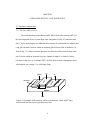
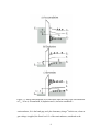
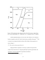
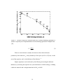
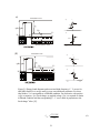
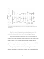
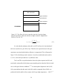
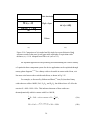
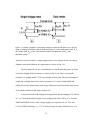
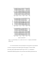
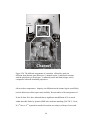
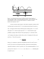
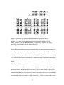
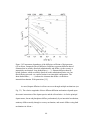
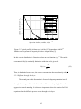
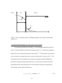
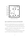
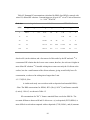
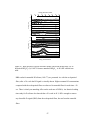
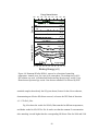
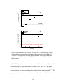
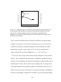
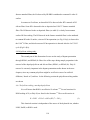
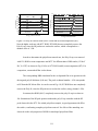
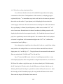
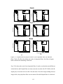
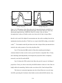
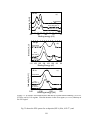
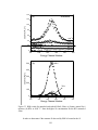
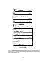
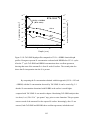
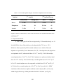
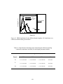
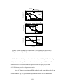
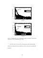
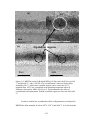
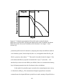
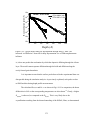
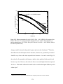
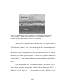
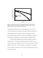
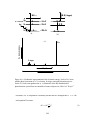
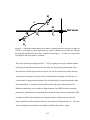
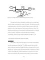
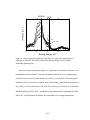
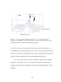
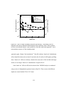
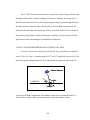
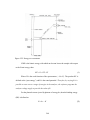
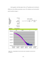
Figure 2.10 Calculated Band offsets for oxide in Si. Reproduced with permission of
the authors.26
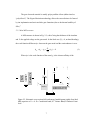
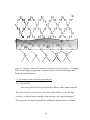
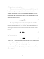
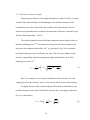
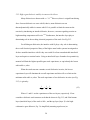
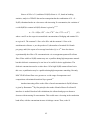
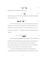
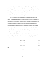
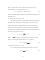
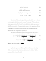
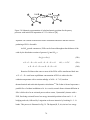
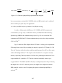
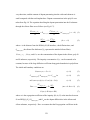
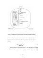
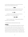
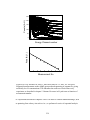
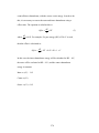
Here l is the interval of separation between adjacent hopping sites, n* is the
density of free electrons in the dielectric, and Γ is the mean hopping frequency.
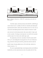
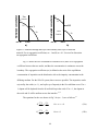
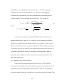
A gate dielectric must have a sufficient ∆EC value to the polysilicon gate (see
section 2.1), and to other gate materials, in order to obtain low off-state currents (leakage
current). If ∆EC is < 1.0 eV, it will likely prevent the oxide’s use in gate dielectric
applications because thermal emission or tunneling would lead to an unacceptably high
leakage current. If VT could also be reduced this problem would be solved.
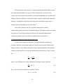
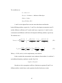
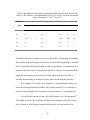
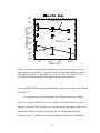
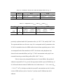
Most potential gate dielectrics do not have reported ∆EC values; the closest
indicator is the band gap (E G) of the dielectric. Generally, large EG corresponds to large
22