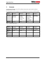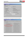
1
Visit us at www.hitex.de, www.hitex.co.uk
or www.hitex.com
Hitex Germany
(Head Quarters)
Hitex UK
Greschbachstr. 12
D-76229 Karlsruhe
+049-721-9628-0
Fax
+049-721-9628-149
E-mail: [email protected]
Warwick University
Science Park
GB Coventry CV47EZ
Hitex USA
2062 Business Center
Drive, Suite 230
Irvine, CA 92612
+44-24-7669-2066
Fax
+44-24-7669-2131
E-mail: [email protected]
Hitex Asia
Fax
E-mail:
800-45-HITEX
+1-949-863-0320
+1-949-863-0331
[email protected]
25 International
Business Park, #04-62A
German Centre
Singapore 609916
+65-6566-7919
Fax
+65-6563-7539
E-mail: [email protected]
Application Note
Debugging the TriCore TC1796
How to use the PCP
This documentation demonstrates how to use the
PCP of the TriCore TC1796 and debug it with the
Tanto debug system.
Architecture:
TriCore
Author:
Peter Walk (Hitex GmbH, T&I)
Revision:
08/2005 - 001
ApplicationNote.dot - 07/2004 - 00
© Copyright 2005 - Hitex Development Tools GmbH
All rights reserved. No part of this document may be copied or reproduced in any form or by any means without prior written consent of Hitex Development Tools. Hitex Development Tools retains
the right to make changes to these specifications at any time, without notice. Hitex Development Tools makes no commitment to update nor to keep current the information contained in this
document. Hitex Development Tools makes no warranty of any kind with regard to this material, including, but not limited to, the implied warranties of merchantability and fitness for a particular
purpose. Hitex Development Tools assumes no responsibility for any errors that may appear in this document. DProbe, Hitex, HiTOP, Tanto, and Tantino are trademarks of Hitex Development
Tools. All trademarks of other companies used in this document refer exclusively to the products of these companies.
Application Note
Preface
In order to keep you up-to-date with the latest developments on our products, we provide Application
Notes containing additional topics, special hints, examples and detailed procedures etc.
For more information on the current software and hardware revisions, as well as our update service,
please contact www.hitex.de, www.hitex.co.uk or www.hitex.com.
Contents
1
Introduction
3
2
About PCP
3
3
3.1
3.1.1
3.1.2
3.2
3.2.1
3.2.2
3.2.3
3.2.4
3.3
3.3.1
3.3.2
Example
Debug Session
Preparing the Session
Using the Example Project
Generating Framework with DAvE
Configuring GPTA
Configuring ASC0
Configuring PCP
Generating Code
Setup Tasking Project
Making the Project
Customizing Code
4
7
7
7
10
13
24
27
28
29
29
31
Appendix
32
© Copyright 2005 Hitex Development Tools GmbH
Page 2/34
Application Note
1
Introduction
This application note describes how to debug the TC1796 PCP. We are using HiTOP and the TantoTriCore to debug and DAvE and Tasking VX-Toolset for TriCore v2.2r1 to generate the application.
The evaluation board being used is an Infineon TriBoard - TC1796.300.
The aim of this document is to debug a PCP example with HiTOP. For this, the following has to be
performed:
•
•
•
adjusting the TriCore peripherals using DAvE,
creating an executable using the Tasking Tool chain,
opening the debug session using the Tanto debugger and HiTOP as the user interface.
Note that an example project for the Tanto TriCore can be downloaded from www.hitex.com which will
do the required settings.
2
About PCP
The PCP is a Peripheral Control Processor that relieves the CPU from most of time critical interrupts.
Basically the PCP is to be considered as a conventional processor executing code in response to
interrupts only. Whenever the PCP handles an interrupt, it will use a register set, which depends on
the interrupt priority level currently used. For this reason the term "channel" will be used in this
document.
© Copyright 2005 Hitex Development Tools GmbH
Page 3/34
Application Note
3
Example
To demonstrate the behavior of the PCP four different channels are used to handle four different
interrupts from the TC1796.
The following table shows the assignment of the interrupt/channel to the function in the PCP program.
Channel /
Priority level
Channel 1
Channel 2
Channel 3
Channel 4
Description
Toggles the onboard LED
(Pin 1.15).
Toggles an LED
externally
connected
(Pin 4.7 in this
example).
Simple echo
function at the
serial port ASC0,
storing the
character into a
global variable.
Increments a
global variable.
Used port
Pin 1.15
Pin 4.7
ASC 0
-
Channel 4
Table 1
Example program functions
Channel /
Priority level
Channel 1
Channel 2
Channel 3
Interrupt
GPTA0-SRN14
GPTA0- SRN10
ASC0 receive SRN GPTA0-SRN6
Used timer
array
GPTA0
GPTA0
-
GPTA0
Used timer
cell
GTC16
GTC8
-
GTC0
time
1 sec
0.5 sec
-
1 sec
Table 2
Used timer / interrupts
© Copyright 2005 Hitex Development Tools GmbH
Page 4/34
Application Note
Toggle LED
The codes for channel 1 and channel 2 are identical, except for the port used. The first entry point
from the channel is stored in the CSA. It is preselected with the address from the label
"channel_1"/"channel_2". With the very first interrupt concerning the channel the port is initialized, and
the port is set to low. The PCP runs to the exit command and waits for the next interrupt. From this
point the PCP continues working from next PC to the next exit command and switches the LED on.
With the next interrupt the PCP switches the LED off and runs until exit. The next interrupt causes the
PCP to jump to the label "led_on". This behaviour is the same like with channel 2.
;------------------------------------------; Channel 1, toggle LED P1.15
;------------------------------------------channel_1:
nop
ldl.iu r1, @hi(P1_IOCR12)
ldl.il r1, @lo(P1_IOCR12)
set.f [r1], 0xf, size=16
clr.f [r4], 0xf
nop
exit ec=0, st=0, int=0, ep=1, cc_uc
nop
led_on:
clr.f [r4], 0xf
nop
exit ec=0, st=0, int=0, ep=1, cc_uc
nop
led_off:
set.f [r4], 0xf
nop
exit ec=0, st=0, int=0, ep=1, cc_uc
nop
jl led_on
;
;
;
;
Initialize port P1:
port control register 12
Set pin P1.15 to Output
Set pin P1.15 to Low
; Exit, no interrupts, start @next PC
; Swith LED on
; Clear P1.15
; Exit, no interrupt, start @ next PC
; Switch LED off
; Set P1.15
; Exit, no interrupt, start @ next PC
; Loop
;-----------------------------------------------;
; .pcpdata'
;-----------------------------------------------;
ch1:
.word
.word
.word
.word
.word
.word
.word
.word
(channel_1 << 16) | 0x0140
0x00010000
0x0
P1_OUT
0x0
0x0
0x0
0x0
;
;
;
;
;
;
;
;
R7 DPTR 0x1, chan.enable
R6 CPU Interrupt Configuration
R5
R4 P1 Output Register
R3
R2
R1
R0
.word
.word
.word
.word
.word
.word
.word
.word
(channel_2 << 16) | 0x0140
0x00010000
0x0
P4_OUT
0x0
0x0
0x0
0x0
;
;
;
;
;
;
;
;
R7 DPTR 0x1, chan.enable
R6 CPU Interrupt Configuration
R5
R4 P4 Output Register
R3
R2
R1
R0
ch2:
© Copyright 2005 Hitex Development Tools GmbH
Page 5/34
Application Note
Local Echo
With each interrupt from the ASC0 the PCP loads the ASC0 receive buffer and transfers it into the
ASC0 transmit buffer. Additionally, the transmit buffer will be copied into R3, that is the cBufPCP
variable in the main program. After the next interrupt, the PCP jumps to the beginning of this code part
and runs up to the exit command.
;------------------------------------------; Channel 3, local echo on ASC0, transfer
;
value to R3 -> global variable
;------------------------------------------channel_3:
LD.F R1, [R4], SIZE=32
nop
ST.F R1, [R5], SIZE=32
nop
ST.F R1, [R3], SIZE=32
nop
EXIT EC=0, ST=0, INT=0, EP=1, cc_UC
nop
jl channel_3
;-----------------------------------------------;
; .pcpdata'
;-----------------------------------------------;
ch3:
.word (channel_3 << 16) | 0x0140
.word 0x01000000
.word ASC0_TBUF_addr
.word ASC0_RBUF_addr
.word cBufPCP
.word 0x00000000
.word 0x00000000
.word 0x00000000
; R1 = ASC0 Receive Buffer
; ASC0 Transmit Buffer = R1
; ASC0 Transmit Buffer -> R3 -> cBufPCP
; exit, no interrupt, start @ next PC
;
;
;
;
;
;
;
;
R7 channel enable set, DPTR=0
R6 CPU Interrupt Configuration
R5
R4
R3
R2
R1
R0
Increment
With the first interrupt concerning this channel the PCP loads the contents from the variable
lGlobalCounterPCP into the register R1, increments it by 1 and then stores it back to the variable.
After an interrupt the PCP jumps to the beginning of this section, repeats the procedure and halts on
the "exit" command.
;------------------------------------------; Channel 4, increases R5 -> global variable
;------------------------------------------channel_4:
LD.i R1, 0x1
nop
ADD.F R1, [R5], SIZE=32
nop
ST.F R1, [R5], SIZE=32
nop
EXIT EC=0, ST=0, INT=0, EP=1, cc_UC
nop
jl channel_4
ch4:
.word
.word
.word
.word
.word
.word
.word
.word
(channel_4 << 16) | 0x0140
0x01000000
lGlobalCounterPCP
0x00000000
0x00000000
0x00000000
0x00000000
0x00000000
© Copyright 2005 Hitex Development Tools GmbH
;exit, no interrupt, channel start @ next PC
;R7 channel enable set, DPTR=0
;R6 CPPN=1
;R5
;R4
;R3
;R2
;R1
;R0
Page 6/34
Application Note
3.1
Debug Session
In order to get a quick entry in debugging the PCP, a ready-to-start example is available from
www.hitex.com. If you want to generate a project from scratch, you have to initialize the TriCore's
SFRs and then generate an executable file. For more information on how to do this refer to p. 31ff.
In this section the first debug session using the Tanto debugger and the HiTOP user interface is
described.
3.1.1 Preparing the Session
To work properly with this example, some assumptions must be made:
1. A debugger must be connected to the target.
2. For testing the ASC0 interrupt, a serial interface must be connected to the board and a terminal
program should be opened. For this example we use the following settings:
• Baud rate 9 600
• Stop bit 1
• Parity none
3. If you want to use a preconfigured project, you should download the example from www.hitex.com
and extract this zip file into a folder. From here you may load the HiTOP example project into the
target (see below).
3.1.2
•
•
Using the Example Project
Start HiTOP and execute HiTOP's Project > Open command.
Select the example project PCPTimerASC.htp from the directory, you had copied the example to.
© Copyright 2005 Hitex Development Tools GmbH
Page 7/34
Application Note
The following dialog will be displayed:
•
Click OK to download the application tc1796_pcpdemo. After downloading, HiTOP will look like
this or similar:
Before starting the emulation set the PC has to be set to 0xA1000000, because the example
application is linked to this address and the Starterkits usually reset to 0xA0000000, depending on the
hardware configuration options. For more information see the Tricore Starterkit User Manual.
© Copyright 2005 Hitex Development Tools GmbH
Page 8/34
Application Note
•
To perform a target reset setting the PC, use the SetPC script button provided in the toolbar:
The script linked to this button additionally performs a "Go until main" to ensure that the PCP code is
copied into RAM.
•
Start the emulation of the TC1796's TriCore by using the F5 key or by clicking on the Go button:
An LED should blink at regular intervals.
•
•
In the Source window, switch to the PCP tab.
To debug the PCP, set a breakpoint, e.g. at address PCPCODE:0xXXXXXXXXXX. The PCP will
stop the execution with the PCP PC on the breakpoint's address.
With a single step (F9 or F11) you can step through the code and turn on or off the LED.
To jump into another channel you just have to set the breakpoints to the following addresses:
•
•
Channel
Start Address
Breakpoint Address
1
PCPCODE:0x00000000
PCPCODE:0x00000009
2
PCPCODE:0x00000013
PCPCODE:0x0000001C
3
PCPCODE:0x00000027
PCPCODE:0x00000027
4
PCPCODE:0x00000030
PCPCODE:0x00000030
Note
Channel 1, 2 and 4 are triggered periodically from the timer. Channel 3 will be triggered from the serial
interface. To stop at a breakpoint you must send a character via the serial interface.
© Copyright 2005 Hitex Development Tools GmbH
Page 9/34
Application Note
3.2
Generating Framework with DAvE
To work properly with the TriCore and the PCP you have to configure all TriCore SFRs. With DAvE,
Infineon's Digital Application virtual Engineer, you may create a framework of functions initializing your
SFRs. In the following the settings being different to DAvE's default settings are presented.
•
Start DAvE and create a new TC1796 project. In the General tab of the Project Settings dialog,
select the correct compiler settings:
•
In the following dialog you may select your system clock.
These settings depend on the target in use. In this example Infineon's TC1796 Starterkit is used
working properly with the following configuration:
© Copyright 2005 Hitex Development Tools GmbH
Page 10/34
Application Note
•
Do not forget to enable the Interrupt System …
© Copyright 2005 Hitex Development Tools GmbH
Page 11/34
Application Note
•
… and the PCP System:
© Copyright 2005 Hitex Development Tools GmbH
Page 12/34
Application Note
3.2.1
Configuring GPTA
First step is to assign the timer settings to the GPTA.
•
Click on the GPTA clock area (red-marked in the figure below) and use the following settings:
© Copyright 2005 Hitex Development Tools GmbH
Page 13/34
Application Note
After configuring the GPTA clock module, the Clock Distribution Unit has to be configured. This unit
dispenses the clock onto seven different clock busses.
•
Click on the CDU button (see below) and make the settings displayed. Only the clock bus 7 will be
different from the default values.
© Copyright 2005 Hitex Development Tools GmbH
Page 14/34
Application Note
In the following steps the Global timer 0 and Global timer 1 are configured.
•
Click on the GTO and GT1 buttons and make the settings displayed.
© Copyright 2005 Hitex Development Tools GmbH
Page 15/34
Application Note
The Global timer 1 interrupts every ½ second.
© Copyright 2005 Hitex Development Tools GmbH
Page 16/34
Application Note
To get different interrupts, we use the global timer cells 0, 8 and 16. Each cell we assign to one SRN
of the TriCore. First configure the timer cells.
•
Click on the GTC, GTC8 and GTC16 buttons and make the suggested settings.
© Copyright 2005 Hitex Development Tools GmbH
Page 17/34
Application Note
© Copyright 2005 Hitex Development Tools GmbH
Page 18/34
Application Note
© Copyright 2005 Hitex Development Tools GmbH
Page 19/34
Application Note
After configuring the timer, the service request nodes of the GPTA must be defined.
•
Use the buttons marked in the following figures, and then make the required settings.
© Copyright 2005 Hitex Development Tools GmbH
Page 20/34
Application Note
© Copyright 2005 Hitex Development Tools GmbH
Page 21/34
Application Note
© Copyright 2005 Hitex Development Tools GmbH
Page 22/34
Application Note
•
Finally select the functions you want to be created by DAvE. Select at least GPTA0_vInit.
Note
DAvE will create any source file only if you selected the init function.
© Copyright 2005 Hitex Development Tools GmbH
Page 23/34
Application Note
3.2.2
Configuring ASC0
To get interrupts from the serial port you will have to configure ASC0.
•
In the DAvE main screen click on the ASC0 peripheral (red-marked in the figure below) and make
the following settings.
© Copyright 2005 Hitex Development Tools GmbH
Page 24/34
Application Note
© Copyright 2005 Hitex Development Tools GmbH
Page 25/34
Application Note
Note
DAvE will create any source file only if you selected the init function.
© Copyright 2005 Hitex Development Tools GmbH
Page 26/34
Application Note
3.2.3
Configuring PCP
In this section the real PCP will be configured.
•
Click on the PCP peripheral (red-marked in the figure below) and make the following settings:
•
Activate the PCP:
© Copyright 2005 Hitex Development Tools GmbH
Page 27/34
Application Note
•
The last step to be done by DAvE is assigning the interrupt levels:
On the right, all available interrupts not being distributed are listed.
•
Drag and drop them into the CPU Interrupt column on the left.
Note
The interrupt level in this column corresponds to the channel used. In this example it is recommended
to use exactly these settings
3.2.4
•
Generating Code
To generate code, click on the toolbar button (red-marked in the figure below). Select a directory
you want save your code.
© Copyright 2005 Hitex Development Tools GmbH
Page 28/34
Application Note
3.3
Setup Tasking Project
3.3.1
Making the Project
The generated files will have to be added to the Tasking project. (For information on how to generate a
new Tasking Project, refer to the Manufacturer's Manual.)
In the following we give some hints different to the default settings the Tasking Toolset will use.
•
Select the correct target processor.
•
Disable the initialization from the bus configuration settings. These settings will be done by HiTOP.
© Copyright 2005 Hitex Development Tools GmbH
Page 29/34
Application Note
•
Disable the automatic inclusion of .sfr file. These files will be generated by DAvE.
•
Disable the default allocation. Otherwise you will get error messages from the Tasking compiler
caused by a compiler bug.
© Copyright 2005 Hitex Development Tools GmbH
Page 30/34
Application Note
3.3.2
Customizing Code
The code created by DAvE, is only a frame of functions which have to be customized. To get the
example running you should insert the following sections.
In the created code the following sections are embedded in the source:
// USER CODE BEGIN (Main,9)
// USER CODE END
Code inserted between these keywords, will not be changed by DAvE in the following.
The table below gives an overview on files and sections you have to change.
*)
File
Section
Contents
main.c
MAIN_General,7
unsigned long lGlobalCounter;
unsigned long lGlobalCounterPCP;
char
cBufPCP;
main.c
Main,9
while (1) ;
main.c
Init,3
pcpInit.c *)
--
initPCP();
#include "main.h"
/* This function initializes the PCP unit:
* - enable PCP
* - channel start PC is taken from restored context
* - use full context save
*/
void initPCP(void)
{
PCP_CS = 0x00020801;
/* Enable PCP, PC from
Context, Full context */
PCP_ICR = 0x03000000;
/* 1 arb. cycles, 2 clocks
per arbitration */
}
Create a new file.
The real PCP (pcpWork.pcp) program will be delivered with the example project (see also the
Appendix on p. 32). You have to add it to the tasking project.
You may now generate the executable using the Tasking Compiler's Make button. This generated
executable can be loaded to the target as described on p. 7ff.
© Copyright 2005 Hitex Development Tools GmbH
Page 31/34
Application Note
Appendix
;***************************************************************************
;**
*
;** FILE
: pcpWork.pcp
*
;**
*
;** DESCRIPTION : PCP Example
*
;**
*
;**************************************************************************/
;
;Definition of symblols
.extern lGlobalCounterPCP
.extern cBufPCP
ASC0_TBUF_addr .equ 0xf0000a20
ASC0_RBUF_addr .equ 0xf0000a24
;address of register ASC0_TBUF
;address of register ASC0_RBUF
;-----------------------------------------------;
; Note:
; A special section name '.pcptext' is used to
; direct the linker/locator to locate this
; section in pcp code. The CODE and INIT
; attributes are used to force this section to
; be copied at the start-up of the program to
; 'pcode' memory.
;-----------------------------------------------;
.sdecl ".pcptext", CODE, INIT
.sect ".pcptext"
;------------------------------------------; Channel 1, toggle LED P1.15
;------------------------------------------channel_1:
nop
ldl.iu r1, @hi(P1_IOCR12)
ldl.il r1, @lo(P1_IOCR12)
set.f [r1], 0xf, size=16
clr.f [r4], 0xf
nop
exit ec=0, st=0, int=0, ep=1, cc_uc
nop
led_on:
clr.f [r4], 0xf
nop
exit ec=0, st=0, int=0, ep=1, cc_uc
nop
led_off:
set.f [r4], 0xf
nop
exit ec=0, st=0, int=0, ep=1, cc_uc
nop
jl led_on
;------------------------------------------; Channel 2, toggle LED P4.7
;------------------------------------------channel_2:
nop
ldl.iu r1, @hi(P4_IOCR12)
dl.il r1, @lo(P4_IOCR12)
et.f [r1], 0x7, size=16
lr.f [r4], 0x7
op
xit ec=0, st=0, int=0, ep=1, cc_uc
nop
led2_on:
nop
clr.f [r4], 0x7
© Copyright 2005 Hitex Development Tools GmbH
;
;
;
;
Initialize port P1:
port control register 12
Set pin P1.15 to Output
Set pin P1.15 to Low
; Exit, no interrupts, start @next PC
; Swith LED on
; Clear P1.15
; Exit, no interrupt, start @ next PC
; Switch LED off
; Set P1.15
; Exit, no interrupt, start @ next PC
; Loop
;
;
;
;
Initialize port P4:
port control register 12
Set pin P4.7 to Output
Set pin P4.7 to Low
; Exit, no interrupts, start @next PC
; Swith LED on
; Clear P4.7
Page 32/34
Application Note
nop
exit ec=0, st=0, int=0, ep=1, cc_uc
led2_off:
nop
set.f [r4], 0x7
nop
exit ec=0, st=0, int=0, ep=1, cc_uc
nop
jl led2_on
;------------------------------------------; Channel 3, local echo on ASC0, transfer
;
value to R3 -> global variable
;------------------------------------------channel_3:
LD.F R1, [R4], SIZE=32
nop
ST.F R1, [R5], SIZE=32
nop
ST.F R1, [R3], SIZE=32
nop
EXIT EC=0, ST=0, INT=0, EP=1, cc_UC
nop
jl channel_3
;------------------------------------------; Channel 4, increases R5 -> global variable
;------------------------------------------channel_4:
LD.i R1, 0x1
nop
ADD.F R1, [R5], SIZE=32
nop
ST.F R1, [R5], SIZE=32
nop
EXIT EC=0, ST=0, INT=0, EP=1, cc_UC
nop
jl channel_4
; Exit, no interrupt, start @ next PC
; Switch LED off
; Set P4.7
; Exit, no interrupt, start @ next PC
; Loop
; R1 = ASC0 Receive Buffer
; ASC0 Transmit Buffer = R1
; ASC0 Transmit Buffer -> R3 -> cBufPCP
;exit, no interrupt, channel start @ next PC
;exit, no interrupt, channel start @ next PC
;-----------------------------------------------;
; Note:
; A special section name '.pcpdata' is used to
; direct the linker/locator to locate this
; section in pcp data memory (pram). This
; section is initialized at start-up time.
;-----------------------------------------------;
.sdecl ".pcpdata", DATA
.sect ".pcpdata"
ch0:
.word
.word
.word
.word
.word
.word
.word
.word
0x0
0x0
0x0
0x0
0x0
0x0
0x0
0x0
;
;
;
;
;
;
;
;
R7
R6
R5
R4
R3
R2
R1
R0
.word
.word
.word
.word
.word
.word
.word
.word
(channel_1 << 16) | 0x0140
0x00010000
0x0
P1_OUT
0x0
0x0
0x0
0x0
;
;
;
;
;
;
;
;
R7 channel enable set, DPTR=0
R6 CPU Interrupt Configuration
R5
R4 P1 Output Register
R3
R2
R1
R0
ch1:
© Copyright 2005 Hitex Development Tools GmbH
Page 33/34
Application Note
ch2:
.word
.word
.word
.word
.word
.word
.word
.word
(channel_2 << 16) | 0x0140
0x00010000
0x0
P4_OUT
0x0
0x0
0x0
0x0
;
;
;
;
;
;
;
;
R7 channel enable set, DPTR=0
R6 CPU Interrupt Configuration
R5
R4, P4 Output Register
R3
R2
R1
R0
.word
.word
.word
.word
.word
.word
.word
.word
(channel_3 << 16) | 0x0140
0x01000000
ASC0_TBUF_addr
ASC0_RBUF_addr
cBufPCP
0x00000000
0x00000000
0x00000000
;
;
;
;
;
;
;
;
R7 channel enable set, DPTR=0
R6 CPU Interrupt Configuration
R5
R4
R3
R2
R1
R0
.word
.word
.word
.word
.word
.word
.word
.word
(channel_4 << 16) | 0x0140
0x01000000
lGlobalCounterPCP
0x00000000
0x00000000
0x00000000
0x00000000
0x00000000
;
;
;
;
;
;
;
;
R7 channel enable set, DPTR=0
R6 CPU Interrupt Configuration
R5
R4
R3
R2
R1
R0
ch3:
ch4:
; Module End
© Copyright 2005 Hitex Development Tools GmbH
Page 34/34