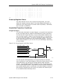
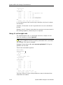
1
Synario ABEL Designer User Manual June 1998 MINC Washington Corp. and Data I/O have made every attempt to ensure that the information in this document is accurate and complete. MINC Washington Corp. and Data I/O assume no liability for errors, or for any incidental, consequential, indirect or special damages, including, without limitation, loss of use, loss or alteration of data, delays, or lost profits or savings, arising from the use of this document or the product which it accompanies. No part of this document may be reproduced or transmitted in any form or by any means, electronic or mechanical, for any purpose without written permission from MINC Washington Corp. and Data I/O . MINC Washington Corp. Sales: 1-888-SYNARIO or [email protected] Technical Support: 1-800-789-6507 or [email protected] World Wide Web: www.synario.com Acknowledgments: MINC is a registered trademark of MINC Incorporated. Data I/O is a registered trademark of Data I/O Corporation. Synario , Synario ECS , and ABEL are either trademarks or registered trademarks of Data I/O Corporation in the United States and/or other countries. Other trademarks are the property of their respective owners. Copyright© 1996-1997 Data I/O Corporation Portions copyright© 1997-1998 MINC Washington Corp. All rights reserved. Table of Contents Preface 1. ABEL Design............................................................................................... 1-1 About this Manual .....................................................................1-1 Programmable IC Design in ABEL ................................................1-1 What is Programmable IC Designing? .....................................1-1 Simulating IC Designs...........................................................1-3 Overview of IC Design ...............................................................1-4 Projects ..............................................................................1-4 Project Sources ....................................................................1-4 Design Simulation and Testing ...............................................1-5 Device Independence............................................................1-5 Vendor Kits .........................................................................1-6 Design Hierarchy..................................................................1-6 How to Use the Project Navigator ................................................1-7 What is the Project Navigator? ...............................................1-7 Why Use the Project Navigator? .............................................1-8 How to Start the Project Navigator .........................................1-8 How the ABEL Project Navigator Works ...................................1-9 Create a New Project in the Project Navigator ........................ 1-13 Open an Existing Project ..................................................... 1-14 Save a project ................................................................... 1-14 Tips for Saving and Naming Projects..................................... 1-15 Change the Title of the Project ............................................. 1-15 Define or Modify the Logic in Your Project.............................. 1-16 Tips for Defining the Logic in the Project ......................... 1-17 Tips for Creating a Top-level Source ............................... 1-18 Import an Existing Source ................................................... 1-19 Remove a Source ............................................................... 1-20 Modify a Source ................................................................. 1-20 Synario ABEL Designer User Manual iii Table of Contents Common Tasks in Programmable IC Design ................................ 1-20 Creating a New IC Design Project ......................................... 1-20 Processing Your Design ....................................................... 1-22 Help, Online Documentation, and Tutorials ................................. 1-23 Help ................................................................................. 1-23 Manuals ............................................................................ 1-23 Tutorials ........................................................................... 1-23 Example IC Designs and Multi-project Simulations ...................... 1-24 Changing the Environment and Configuration ............................. 1-24 2. Hierarchical Design in ABEL..................................................................... 2-1 What Is a Hierarchical Design?....................................................2-1 Why Use Hierarchical Design? .....................................................2-2 Approaches to Hierarchical Design ...............................................2-2 Creating a new Hierarchical Design.........................................2-2 How To Specify a Lower-level Module in an ABEL-HDL Module.........2-3 Hierarchical Design Considerations ..............................................2-6 Prevent Node Collapsing........................................................2-6 3. Overview of ABEL-HDL Sources.............................................................. 3-1 What is ABEL-HDL? ...................................................................3-1 Mixed Design Entry...............................................................3-1 A First Look at a Design using ABEL-HDL Sources..........................3-2 Opening an Existing Design ...................................................3-2 Project Sources ....................................................................3-5 Project Processes .................................................................3-5 Online Help .........................................................................3-6 Examining the Project Sources ...............................................3-6 Creating a PLD Design Consisting of ABEL-HDL Sources .................3-7 Describing the Circuit using ABEL-HDL ....................................3-7 The ABEL-HDL Reference..................................................... 3-10 Creating a Hierarchical ABEL-HDL Design for a CPLD.................... 3-11 Description of the Circuit ..................................................... 3-11 Entering the Circuit ............................................................ 3-11 To change the name of the project (design): ......................... 3-11 Create or Import ABEL-HDL Sources ..................................... 3-12 Using ABEL-HDL Hierarchy .................................................. 3-13 The ABEL-HDL Reference..................................................... 3-14 Creating an FPGA Design using ABEL-HDL .................................. 3-15 Entering the Design ............................................................ 3-15 Create or Import ABEL-HDL Sources ..................................... 3-15 Integrating ABEL-HDL Designs into Larger Circuits ................. 3-23 iv Synario ABEL Designer User Manual Table of Contents The ABEL-HDL Reference..................................................... 3-24 ABEL-HDL Compiling................................................................ 3-24 ABEL-HDL Design Considerations .............................................. 3-24 4. ABEL-HDL Compiling ................................................................................ 4-1 Overview of ABEL-HDL Compiling ................................................4-1 Architecture Independent Compiling ............................................4-1 ABEL-HDL for PLDs ....................................................................4-2 Keeping Track of Processes: Auto-update ...............................4-2 Compiling an ABEL-HDL Source File ........................................4-3 Using Properties and Strategies for PLDs .................................4-5 Simulating the PLD Design ....................................................4-9 ABEL-HDL for CPLDs ................................................................ 4-12 Using Properties and Strategies ........................................... 4-12 Selecting a Device .............................................................. 4-12 Mapping the Design to the Selected Device............................ 4-13 To fit the design into the selected CPLD device: ..................... 4-15 To create a JEDEC format programming data file:................... 4-15 Using Test Vectors for CPLD Simulation................................. 4-15 ABEL-HDL for FPGAs ................................................................ 4-18 Running Processes ............................................................. 4-18 Using Properties and Strategies ........................................... 4-18 Selecting a Device .............................................................. 4-18 Mapping the Design to the Selected Device............................ 4-19 Simulation......................................................................... 4-19 5. Synario ABEL-HDL Design Considerations ............................................ 5-1 Overview of ABEL-HDL Design Considerations ...............................5-1 Hierarchy in ABEL-HDL...............................................................5-1 Instantiating a Lower-level Module in an ABEL-HDL Source........5-2 Hierarchy and Retargeting and Fitting .....................................5-4 Hierarchy and Test Vectors (PLD JEDEC Simulation) .................5-4 Node Collapsing ........................................................................5-5 Selective Collapsing..............................................................5-5 Pin-to-pin Language Features .....................................................5-6 Device-independence vs. Architecture-independence ................5-6 Signal Attributes ..................................................................5-6 Signal Dot Extensions ...........................................................5-6 Pin-to-pin vs. Detailed Descriptions for Registered Designs............5-7 Using := for Pin-to-pin Descriptions........................................5-7 Detailed Circuit Descriptions ..................................................5-8 Synario ABEL Designer User Manual v Table of Contents Examples of Pin-to-pin and Detailed Descriptions ................... 5-10 Detailed Module with Inverted Outputs ................................. 5-11 When to Use Detailed Descriptions ....................................... 5-13 Using := for Alternative Flip-flop Types ................................. 5-13 Using Active-low Declarations ................................................... 5-14 Polarity Control ....................................................................... 5-16 Polarity Control with Istype ................................................. 5-16 Flip-flop Equations .................................................................. 5-17 Feedback Considerations — Dot Extensions ................................ 5-18 Dot Extensions and Architecture-Independence...................... 5-19 Dot Extensions and Detail Design Descriptions ....................... 5-21 Using Don't Care Optimization .................................................. 5-23 Exclusive OR Equations ............................................................ 5-26 Optimizing XOR Devices ...................................................... 5-26 Using XOR Operators in Equations ........................................ 5-26 Using Implied XORs in Equations.......................................... 5-27 Using XORs for Flip-flop Emulation ....................................... 5-27 State Machines ....................................................................... 5-29 Use Identifiers Rather Than Numbers for States ..................... 5-29 Powerup Register States ..................................................... 5-31 Unsatisfied Transition Conditions.......................................... 5-31 Precautions for Using Don't Care Optimization ....................... 5-33 Number Adjacent States for One-bit Change.......................... 5-37 Use State Register Outputs to Identify States ........................ 5-38 Using Symbolic State Descriptions........................................ 5-39 Using Complement Arrays ........................................................ 5-40 ABEL-HDL and Truth Tables ...................................................... 5-43 Basic Syntax - Simple Examples........................................... 5-44 Influence of Signal polarity .................................................. 5-45 Using .X. in Truth tables conditions ...................................... 5-45 Using .X. on the right side ................................................... 5-46 Special case: Empty ON-set................................................. 5-47 Registered Logic in Truth tables ........................................... 5-47 A. Equation Simulation .................................................................................. A-1 Overview of Equation Simulation .................................................A-1 What is Equation Simulation? ................................................A-1 Simulation Flow ...................................................................A-1 The Simulator Model.............................................................A-2 .tmv Vectors........................................................................A-2 How to Use the Equation Simulator .............................................A-3 Test Vector Files...................................................................A-3 vi Synario ABEL Designer User Manual Table of Contents How to Invoke Simulation .....................................................A-4 B. JEDEC Simulation .....................................................................................B-1 What is JEDEC Simulation? .........................................................B-1 What is Equation Simulation? ................................................B-1 Simulation Flow ...................................................................B-1 The Simulator Model.............................................................B-2 JEDEC and .tmv Vectors ........................................................B-3 How to Use the JEDEC Simulator .................................................B-4 Test Vector Files...................................................................B-4 How to Invoke Simulation .....................................................B-6 C. Waveform Viewing.....................................................................................C-1 What is Waveform Viewing/Editing?.............................................C-1 Starting the Waveform Viewer ....................................................C-2 Waveform Viewer Window .....................................................C-3 Selecting the Waveforms to View ................................................C-4 Show ..................................................................................C-4 Duplicate ............................................................................C-5 Move ..................................................................................C-5 Hide ...................................................................................C-5 Selecting the Bus-Value Radix ...............................................C-5 Moving Around..........................................................................C-6 View Commands ..................................................................C-6 Scroll Bars...........................................................................C-6 Moving the Query Cursor.......................................................C-7 Jumping to Events................................................................C-7 Triggers ..............................................................................C-8 Analysis Techniques ..................................................................C-8 Logic Level and Time Measurements .......................................C-8 Interaction with the Hierarchy Navigator .................................C-9 Displaying Simulation Values on a Schematic ..........................C-9 View Report.........................................................................C-9 Saving and Printing Waveforms................................................. C-10 Saving Waveforms ............................................................. C-10 Printing Waveforms ............................................................ C-10 Index Synario ABEL Designer User Manual vii Table of Contents viii Synario ABEL Designer User Manual 1. ABEL Design About this Manual This manual discusses Programmable IC entry, testing, and design in ABEL. This manual assumes that you have a basic understanding of IC design. If you are using the Programmable IC Designer product instead of ABEL Designer, please refer to the Synario Programmable IC Designer User Manual for information on IC Design. The information in this manual is intended for ABEL users. Programmable IC Design in ABEL What is Programmable IC Designing? Programmable IC designing is creating a design that can be implemented into a programmable IC (also called a chip or device). PLDs (Programmable Logic Devices) and CPLDs (Complex PLDs) are a few examples of programmable ICs. Figure 1-1 on the next page shows an example IC Design. This design has lower-level ABEL-HDL files (not shown). ABEL uses the Project Navigator interface as the front-end to all the design tools in the ABEL Designer. The Project Navigator creates an integrated design environment that links together proprietary and third-party design, simulation, and place-and-route tools. For instance, we believe the people that know the most about programmable ICs are the people who manufacture them. The Project Navigator links together our design tools with place-and-route tools created by us in close cooperation with the IC vendors or by the IC vendors themselves. Synario ABEL Designer User Manual 1-1 ABEL Design Figure 1-1: Example of a Top-level ABEL-HDL source for a IC Design MODULE twocnt TITLE 'two counters having a race' "Demonstrates ability to use multiple levels of ABEL-HDL Hierarchy, "and to collapse lower-level module nodes into upper level modules. "For example, each counter has four REGISTER nodes, and this module "has four COMBINATORIAL pins. The lower-level registers are correctly "flattened into the top-level combinatorial outputs. No dot extensions "are used, allowing the system to determine the best feedback path to use. "This design uses the advanced fit properties REMOVE REDUNDANT NODES "and MERGE EQUIVALENT FEEDBACK NODES. "Constants c,x = .c.,.x.; "Inputs clk, en1, en2, rst pin ; "Outputs a3, a2, a1, a0, b3, b2, b1, b0 pin ; ov1, ov2 pin istype 'reg,buffer'; "Submodule declarations hiercnt interface (clk,rst,en -> q3, q2, q1, q0); "Submodule instances cnt1 functional_block hiercnt; cnt2 functional_block hiercnt; Equations cnt1.clk = clk; cnt2.clk = clk; cnt1.rst = rst; cnt2.rst = rst; cnt1.en = en1; "Each counter may be enabled independent of cnt2.en = en2; "the other. This module may be used as a "Sub-module for a higher-level design, as these "counters may be cascaded by feeding the ov "outputs to the en inputs of the next stage. ov1.clk = clk; ov2.clk = clk; ov1 := a3 & a2 & a1 & !a0 & en1; "look-ahead carry - overflow ov2 := b3 & b2 & b1 & !b0 & en2; "indicator a3 = cnt1.q3; a2 = cnt1.q2; a1 = cnt1.q1; a0 = cnt1.q0; b3 = cnt2.q3; b2 = cnt2.q2; b1 = cnt2.q1; b0 = cnt2.q0; test_vectors ([clk,rst,en1,en2] -> [a3,a2,a1,a0,b3,b2,b1,b0,ov1,ov2]) [ 0 , 0, 0 , 0 ] -> [ x, x, x, x, x, x, x, x, x, x ]; [ c , 1, 0 , 0 ] -> [ 0, 0, 0, 0, 0, 0, 0, 0, 0, 0 ]; [ c , 0, 1 , 0 ] -> [ 0, 0, 0, 1, 0, 0, 0, 0, 0, 0 ]; [ c , 0, 1 , 0 ] -> [ 0, 0, 1, 0, 0, 0, 0, 0, 0, 0 ]; [ c , 0, 1 , 0 ] -> [ 0, 0, 1, 1, 0, 0, 0, 0, 0, 0 ]; [ c , 0, 0 , 1 ] -> [ 0, 0, 1, 1, 0, 0, 0, 1, 0, 0 ]; [ c , 0, 0 , 1 ] -> [ 0, 0, 1, 1, 0, 0, 1, 0, 0, 0 ]; END 1-2 Synario ABEL Designer User Manual ABEL Design In ABEL, a single IC is represented by a single project that is created and modified using the ABEL Project Navigator. The project contains all the logical descriptions for the IC. In addition, the project can contain documentation files, simulation models, and test files (you can associate test files with a piece of the design or the entire design depending on what you want simulated). A project represents one IC design, but you have the option of targeting your design to a specific IC vendor's device or to a virtual device. When you switch the target device, the processes and design flow in the Project Navigator changes to one that is appropriate for the new target device. For example, Figure 1-2 shows the sources as they appear in the Project Navigator for an example IC Design project. Figure 1-2: Sources in an Example IC Design Project Project Title Targeted Device ABEL-HDL Test Vectors Lower-level ABEL-HDL file Lower-level ABEL-HDL file In Figure 1-2, the top-level ABEL-HDL file (twocnt) contains Interface statements that instantiate (links to) the lower-level ABEL-HDL file called hiercnt. Simulating IC Designs You can use JEDEC and Equation simulation on your ABEL-HDL test vectors to simulate your design. Synario ABEL Designer User Manual 1-3 ABEL Design Overview of IC Design With ABEL, you can create and test designs that will be physically implemented into Programmable ICs (also called chips and devices). Projects IC Designs are built in the Project Navigator using a project. In the Project Navigator, one project represents one IC. For more information about creating projects, refer to the rest of this chapter. Project Sources In ABEL, projects consist of ABEL-HDL sources. For more information about ABEL-HDL sources, refer to Chapters 3, 4, and 5. 1-4 Synario ABEL Designer User Manual ABEL Design Design Simulation and Testing Equation and JEDEC simulation is available using ABEL-HDL Test Vector (.abv) files. For more information about simulation: • For Equation simulation, refer to Appendix A. • For JEDEC simulation, refer to Appendix B. • For Waveform viewing, refer to Appendix C. Device Independence By targeting your design to a Virtual Device, you can create designs that are portable to different device architectures. You can later select a specific device family to target your design to so that you can physically implement your design into a specific device. Many processes for IC Designs can be conducted using a "Virtual Device." For instance, you can Functionally Simulate an IC Design targeted to a Virtual Device. Because ABEL's Project Navigator is context sensitive (changes with the context of your design), when you choose a Virtual Device, only those processes allowed for a virtual device are shown. If you choose a specific device family, the processes change to reflect your selection (the processes should be those allowed for a Virtual Device plus those specific to the device architecture you have selected). Synario ABEL Designer User Manual 1-5 ABEL Design Vendor Kits IC designs are physically implemented into a chip more efficiently when the design is optimized and routed for the IC. For example, fitters and place-and-route software designed for the target IC can utilize special features of the IC and map the resource usage more efficiently. The Vendor Kit (Device Kit or Interface Kit) not only controls the processes that are available, but it also changes the entire design environment (such as the default property values) for the target device architecture. Depending on which semiconductor vendor you prefer the most, you can purchase a Vendor Kit that supports the ICs (such as PLDs and FPGAs) for that vendor. For information about a Vendor Kit, refer to the documentation included with the Device Kit or Interface Kit. Design Hierarchy When designs can be broken into multiple levels, this is called hierarchical designing. ABEL supports full hierarchical design, which permits you to create a design that is divided into multiple levels, either to clarify its function or permit the easy reuse of functional blocks. For instance, a large, complex design does not have to be created as a single module. By using hierarchical designing, each component or piece of a complex design could be created as a separate module. For more information on hierarchical designing, refer to Chapter 2. 1-6 Synario ABEL Designer User Manual ABEL Design How to Use the Project Navigator Figure 1-3: ABEL Project Navigator What is the Project Navigator? The Project Navigator is the primary interface for accessing ABEL Designer. Since ABEL consists of many parts, the Project Navigator connects all the pieces in a seamless environment. The Project Navigator supports top-down design through the concept of sub-projects. A designer can create a top-level block diagram that represents a system, which may be an IC, ICs on boards, a board, or a set of boards. As a designer further defines the system, each level can be identified as a sub-project type− designing it as an IC Design or Multi-project Simulation. For example, from the Project Navigator, you can select all the components for a design, such as HDL sources, as well as specification documents and test files. The Project Navigator helps you keep track of all of the parts of your design, and keeps track of the processing steps necessary to move the design from the conceptual stage through to implementation in an actual programmable IC. The Project Navigator integrates many tools for design entry. For example, for ABEL-HDL source files, the Project Navigator connects to the ABEL Text Editor or an Editor of your choice. Synario ABEL Designer User Manual 1-7 ABEL Design Why Use the Project Navigator? There are many different tools for the many different tasks involved in making and testing your design. The Project Navigator is a way of integrating the different tools. The Project Navigator also keeps track of both the parts of your design and the states that each part is in so you can spend less time thinking about which steps and processes need to be run, and more time developing your designs. The Project Navigator also keeps track of preferences for you, automatically setting the options that work for most systems until you want to tweak the options for yourself. How to Start the Project Navigator After installing your ABEL products, do the following to start the Project Navigator. (Refer to the Release Notes included with ABEL for instructions on how to install ABEL products.) For Windows 95/98 and Windows NT Installations 1. Click on the Start button, and then select the following from the Start menus: a) Programs b) ABEL X.X (where X.X is the current version of ABEL) c) ABEL After the program loads, the Project Navigator window appears. 1-8 Synario ABEL Designer User Manual ABEL Design How the ABEL Project Navigator Works ABEL employs the concept of a project. A project is a design. Each project has its own directory in which all source files, intermediate data files, and resulting files are stored. The picture shown below shows an example of what the Project Navigator might look like with a programmable IC project (called multi.syn) opened. The Sources in Project Window (Sources window) shows all the design files associated with a project. The Processes for Current Source Window (Processes window) shows the available processes for the selected source. Notebook Icon ( ) This picture shows the Project Navigator after a programmable IC project is opened. If no project is open, the Sources and Processes windows would be empty. Synario ABEL Designer User Manual 1-9 ABEL Design The Sources Window The Sources window (on the left side of the Project Navigator) shows all the design files associated with a project. Each object in the list is identified with an icon. For example, at the top of the Sources window is the Project Notebook ; it is denoted with the engineering-notebook icon. In multi, the Project Notebook is labeled as "three bit multiplier." (To see all the objects in the project, use the scroll bar at the right edge of the Sources window to move up and down in the list.) There are several kinds of design sources in ABEL, including ABEL-HDL modules, and ABEL-HDL test vectors for simulation. The Notebook Icon ( ) In the Project Navigator Sources window, projects are organized by collecting all of a project's files into a Project Notebook (represented by the notebook icon ( )). The Project Notebook lists the schematics and behavioral sources that create the logic of your design, testing files, and the device specification. The Project Notebook can also include any other design documents you want to keep with the design, such as design specifications, meeting notes or other supplementary files. Each project is stored in its own directory to simplify archiving. To rename the project, double-click the project icon ( ) in the Source window. Project Sources Your design can be represented in various ways. Those representations are called sources. A source is any element in the design such as a HDL file, schematic, or simulation file. Sources are displayed in the Project Navigator Source's Window. They include not only the description of the circuits, as represented by schematics, state diagrams, and hardware description languages, but also include waveforms for simulation, simulation test fixtures, links that connect represent connections to other projects, and documentation of the design. All those pieces are part of the whole design, which includes not only the circuits but the things you need to do to assure yourself that those circuits work as they ought to. The design description (logic) for a project is contained ABEL-HDL sources. One source file in a project is the top-level source for the design. The top-level source defines the inputs and outputs that will be mapped into the device, and references the logic descriptions contained in lower-level sources. The referencing of another source is called “instantiation.” Lower-level sources can also instantiate sources to build as many levels of logic as necessary to describe your design. 1-10 Synario ABEL Designer User Manual ABEL Design If you build a project with a single source, that source is automatically the top-level source. You might have sources other than ABEL-HDL modules. These sources might include simulation test vectors, documentation files, or other files related to Windows applications. The type of a source is indicated by the icon to the left of the source name in the Sources Window. Listed below are the sources for the project. When you begin a new project there won’ t be any sources except for the project notebook. For most of the tools to work, there needs to be only one top-level source, which must be the root source for all the other sources in the project. This structure can usually be done with a single top level schematic that represents the entire system, and that schematic then calls out all the parts. Table 1-1: Types of Sources in the Project Navigator Source Type Icon File Extension Project notebook if at top of the Sources Window (see "linked project" below) .syn Document File (such as a specification) .wri, .doc, .hlp (or any extension not recognized by Project Navigator) Targeted Device Family (appears in all IC Design projects) .fdk ABEL-HDL logic description .abl ABEL-HDL test vectors .abv (or .abl) State Diagram (optional) .dia Waveform stimulus .wdl Undefined or incorrect source reference ABEL-HDL source that failed Update Hierarchy process Synario ABEL Designer User Manual .abl 1-11 ABEL Design The Processes Window The Processes window (on the right side of the Project Navigator) shows all the processing tasks that apply to whatever object or file is highlighted in the Sources window (on the left side). A processing task includes: netlisting, compiling, logic reduction, logic synthesis, place and routing, simulation model-building — in other words, any step along the way from design entry to implemented IC, system, or board. Design Flows in the Processes Window One of ABEL’ s most powerful features is that it knows how to process any kind of design for any kind of architecture because the Project Navigator is context sensitive (which helps prevent information overload). The steps in the Processes window are context sensitive in two ways. First, the processes change depending on what kind of source file you’ ve highlighted in the Sources window (source-level flow). Second, the processing for a given file changes depends on what target device kit you’ ve chosen (project-level flow). For instance, a schematic targeted for an XYZ PLD is processed differently than a schematic targeted for an ABC PLD. Project-level Design Flow For IC Design projects, click on the device icon ( ) in the Sources Window. The processes that appear in the Processes Window represent the Project-level Design Flow. Source-level Design Flow Click on any source (such as a schematic or HDL source) in the Sources Window. The processes that appear in the Processes Window (if any) represent the Source-level Design Flow. 1-12 Synario ABEL Designer User Manual ABEL Design Create a New Project in the Project Navigator After starting the Project Navigator (see page 1-8 for instructions), you can create a new project by doing the following: 1. In the Project Navigator's File menu, click on New Project. A project contains the sources and processes for a single IC (also called chip or device) design, and if you have various Vendor Kits, you’ ll be able to pick various technologies with which to implement that IC. The IC projects have the flexibility to change devices if the design is done with the virtual device libraries and symbols. 2. In the Create New Project dialog box, enter a name for the project file (.syn) that will be used for your design. The project name can be up to 8 characters long plus the .syn extension. 3. Choose the directory in which you want to place your project files. You can navigate through the directories and click on the Create Dir… button to create additional directories. When you are finished navigating to the directory for the project, click on the OK button. We do not recommend placing more than one project in the same directory. You can use the Create Directory button to create a meaningful structure of directories to hold each project. 4. The project appears in the Sources window of the Project Navigator. Double-click on the title of the project, "Untitled." The Project Title dialog box appears. 5. In the Project Title dialog box, enter the name you want for your project, and then click on the OK button. The project title can be as long as you like, but only the first 20 characters will show. The title can contain spaces and any other keyboard character except tabs and returns. Synario ABEL Designer User Manual 1-13 ABEL Design For some device kits, the project directory and project name should be the same. 6. In the Project Navigator's File menu, click on Save to save your project. Open an Existing Project 1. In the Project Navigator's File menu, click on Open Project. The Open Project dialog box appears. 2. Find the project file (.syn) you wish to open. 3. Click on the file and then click on the OK button. If you get an error, “Cannot create Hierarchy,”when trying to open a project, make sure you have write privileges in the project directory and that the disk has free space for temporary files. Save a project To save a project: Select Save or Save As from the File menu. If you select Save As, ABEL asks for a filename to save the project to. What is Saved Saving a project saves a project file (.syn extension) with the following information: • The title of the project • The sources in the project • The strategy associated with each source (.sty extension) ABEL also tells the text editor to save when you save a project. When you select Save As to save a project to another directory, ABEL copies all of the project files to that directory. 1-14 Synario ABEL Designer User Manual ABEL Design Tips for Saving and Naming Projects Use the following guidelines when saving and naming source files and projects: • Avoid saving more than one project in the same directory. • Use the Create Directory option to save linked projects in subdirectories of the top-level project. This will allow you to later reference the linked projects using relative paths (which will allow you to move your design files without having to relink projects). • Avoid saving a project which has the same base file name as one of its sources. If a source and project have the same base name, you may have problems with the Project Navigator's automake feature. For instance, avoid calling your project "myfile.syn" if it contains a source named "myfile.abl." Change the Title of the Project Do the following to change the title of an open project. 1. The project appears in the Sources window of the Project Navigator. Double-click on the title of the project. The Project Title dialog box appears. 2. In the Project Title dialog box, enter the name you want for your project, and then click on the OK button. The project title can be as long as you like, but only the first 20 characters will show. The title can contain spaces and any other keyboard character except tabs and returns. For some Vendor Kits, the project directory and project name should be the same. Synario ABEL Designer User Manual 1-15 ABEL Design Define or Modify the Logic in Your Project You define the logic in a design with the project sources. These sources can be created from scratch using an available editor, or you can import an existing source. You have the following choices to define the logic of your project: 1. 2. 3. 4. Create new sources Import existing sources Remove sources Modify sources Defining the logic of your design is probably one of the most difficult tasks because it can involve many steps, design rules, and design dependencies (hierarchy). The least complex design is a "flat" design in which there is only one source describing the design (such as a single ABEL-HDL file). With a "flat" design, you can add a test file (such as a ABEL-HDL test vectors). All processes (such as JEDEC simulation) in the "flat" design involve the entire design. The complexity of the design increases as you add dependencies (hierarchy). A "hierarchical" or "top-down" design consists of a toplevel source that contains interface statements that link to lower-level modules to create the overall design. The referencing of a lower-level source is called “instantiation.” A source can be referenced (“instantiated”) more than once. Also, a source can be both a lower-level and top-level source. For example, "compare" in the following figure could instantiate another file. The following figure shows what a hierarchical design looks like in the Sources window. Note: If you do not see the filenames in parentheses () and would like to see them, make sure that Filenames is checked in the View menu. 1-16 Synario ABEL Designer User Manual ABEL Design You can change to a "flat" hierarchy view (that shows only the top file) by removing the check on View: Hierarchy. For additional information about building a hierarchical design, refer to chapter 2 in this manual. Tips for Defining the Logic in the Project Use the following guidelines when saving and naming source files and projects: • It is best to create the lowest-level sources first and then import or create the higher-level sources. In other words, don't use topdown design. • Avoid using ABEL-HDL keywords for module and signal names in any of your source files. • Do not use any Vendor-Kit-specific macro functions to name a source. • Avoid saving a project that has the same base file name as one of its sources. If a source and project have the same base name, you may have problems with the Project Navigator's automake feature. For instance, avoid calling your project "myfile.syn" if it contains a source named "myfile.abl." • Each source must have a unique name in the project. Do not have two different sources with the same name. You can use the same source many times in a design by instantiating the source, but two different sources with the same name can cause problems with hierarchy. For example, do not have an top-level source called "Compare" and a lower-level source also called "Compare." Create a New Source You can create a new source and add it to your project by doing the following: 1. From the Source menu, click on New. The New Source dialog box appears. 2. In the New Source dialog box, click on the type of source you would like to create, and then click on the OK button. The Project Navigator starts an editor that you can use to enter the information for your new source. For HDL sources, a text editor is started. Do not name source files the same name as other source files in the same project. Synario ABEL Designer User Manual 1-17 ABEL Design 3. In the editor, create a source. The following table lists the available source types and where to look for more information. To Edit Look Here Behavioral Modules (ABEL-HDL) ABEL-HDL entry section in the Synario Programmable IC Designer User Manual and the ABEL-HDL Reference. Note that ABEL-HDL sources are not supported in Board Design or System Simulation projects User Document The documentation for the editor you will be using. By default, the editor is either a text editor or Microsoft Write (which edits .wri files). Waveform Stimulus Waveform Viewing section later in this manual, (used in simulation) and the documentation for your simulator. See Also: For IC Design projects, refer to the Vendor Kit manual for specific design information about a device family. Tips for Creating a Top-level Source Use the following guidelines when creating a top-level source: • It is best to create the lowest-level sources first and then import or create the higher-level sources. Building a Top-level ABEL-HDL Module • In a top-level behavioral module in ABEL-HDL, you use the Interface and Functional_block keywords to instantiate lower-level files. You can also use the Interface keyword in lower-level files to link to upper-level ABEL-HDL modules (not upper-level schematics). The ABEL-HDL file pwmdac.abl demonstrates the use of the Functional_block and Interface keywords in a top-level file. The file counter.abl demonstrates the use of the Interface keyword in a lower-level file. 1-18 Synario ABEL Designer User Manual ABEL Design Import an Existing Source You can import a source into your project by doing the following: 1. From the Source menu, click on Import. The Import File dialog box appears. 2. Find the source file you wish to import. You can change the type of file that is displayed in the List files of type list box. 3. When you are done selecting the source, click on OK. 4. Depending on the source type you are importing, you may be asked to provide additional information in the Source Type dialog box. 5. Depending on the source you are importing, you may be asked to associate the source with another source in the Associate… dialog box . For example, if you import ABEL-HDL test vectors (.abv) file, you are asked which source to associate the file to. If you choose a behavior description, such as an ABEL-HDL file, the test vector file will only apply to that source. If you choose the device source, the test vector file will apply to testing the entire design It is best to import the lower-level sources before importing upper-level sources. You will get an error message if you import a source that has links to lower-level sources and the lower-level sources are not already part of your project. Import test files that are to be associated with other sources after importing or creating the other source. Where the source file is place in the Project Navigator The new source is entered into the Sources window. Where the source appears in the window depends on the following: • If the imported source is documentation or of a file type not recognized as a logic description or test file, the source appears between the Project Icon ( ) and targeted design icon ( ). • If the source is a logic description, the source is placed in alphabetical order for each level of hierarchy following the project notebook and the targeted device kit. For example, if the source is called "multiplx" and the top-level source, a schematic called "myboard," instantiates "multiplx," the source is placed underneath "myboard" in the Sources window. • If the source is a test file, the source is placed underneath the source that the file is associated with. Synario ABEL Designer User Manual 1-19 ABEL Design Remove a Source 1. From the Sources window, click on the source (the source is highlighted). 2. From the Source menu, click on Remove. Note: Removing a source from a project does not delete the underlying file. Modify a Source You can edit any of the sources that make up your project by double-clicking on them (if you have file associations set up in Windows and have enabled "Use File Associations" in "Options: Environment" in the Project Navigator). See Also: For IC Design projects, refer to the Vendor Kit (Device Kit or Interface Kit) manual for specific design information about a device family. In Windows 95 and NT, you can associate text files with the ABEL Text Editor by using the Windows 95 Explorer. See the documentation for the Windows 95 Explorer for more information. Common Tasks in Programmable IC Design Creating a New IC Design Project A project contains the sources and processes for a single IC Design, and if you have various Device Kits, you’ ll be able to pick various technologies with which to implement that IC. The IC projects have the flexibility to change ICs if the design is done with the virtual chip libraries and symbols After starting the Project Navigator, you can create a new IC design project by doing the following: 1. In the Project Navigator's File menu, click on New Project. 2. In the Create New Project dialog box, enter a name for the project file (.syn) that will be used for your design. The project name can be up to 8 characters long plus the .syn extension. 3. Choose the directory in which you want to place your project files. You can navigate through the directories and click on the Create Dir… button to create additional directories. 1-20 Synario ABEL Designer User Manual ABEL Design When you are finished navigating to the directory for the project, click on the OK button. We do not recommend placing more than one project in the same directory. You can use the Create Directory button to create a meaningful structure of directories to hold each project. 4. The project appears in the Sources window of the Project Navigator. Double-click on the title of the project, "Untitled." The Project Title dialog box appears. 5. In the Project Title dialog box, enter the name you want for your project, and then click on the OK button. The project title can be as long as you like, but only the first 20 characters will show. The title can contain spaces and any other keyboard character except tabs and returns. 6. In the Project Navigator's File menu, click on Save to save your project. 7. Add sources and documentation to your project by using the commands in the Sources menu. You can create new sources or import existing sources into your project. All sources are saved in the same directory as the project (.syn) file. For information on how to build a IC sources, refer to the rest of this manual. To edit a source in the project, double-click on the source in the Project Navigator Sources Window. You can also import sources into your project by drag and dropping the files into the Project Navigator from the Windows File Manager or Explorer. 8. Double-click on the device icon ( box appears. ). The Choose Device dialog 9. In the Choose Device dialog box, click on the Device Family (Kit) and device that you intend to target your design to, and then click on OK. (You can change this later if you wish.) If asked if it is OK to change board kits, click on OK. You do not need to choose a specific device for functional simulation, you can use "Virtual Devices." 10. After adding design source files, you need to add test files to your project for simulation. For instance, import test vector (.abv) files for Equation or JEDEC simulation. 11. Click on sources to see the available processes for each source type. Double-click on a process to run that process. Synario ABEL Designer User Manual 1-21 ABEL Design 12. To place-and-route or fit your design, single-click on the device icon ( ).and double-click on the Fit Design or Place-and-Route process. For more information on IC Designing, refer to the rest of this manual. Processing Your Design When you click on each source in the Project Navigator, a number of processes are brought up. Each process list invokes the tools to do that stage of the process. You can double click on any stage to generate it and see the results. • To run processes that affect the entire project (such as place-androute), in the Processes window, click on the project design icon, and then double-click on the process. • To run simulation on the entire project, click on the test file that is associated with the project design icon (this file should be located directly below the design icon). • To run processes that affect a single source and it's components, in the Processes window, click on the source, and then double-click on the process. • To run simulation on a source, click on the test file that is associated with the source (this file should be located directly below the source). 1-22 Synario ABEL Designer User Manual ABEL Design Help, Online Documentation, and Tutorials Help Context sensitive help is available in the Project Navigator by: • Clicking on the Context Help button ( item you want information on. ), and then clicking on the • Clicking on an item (such as a process), and then pressing the F1 key. • Clicking on the Help button in a dialog box. General help is available by clicking on a menu item in the Help menu. Manuals You can view an online manual using any installed PDF file viewer. The Synario CD ROM includes the Acrobat PDF Viewer. In order to use this viewer, you must install it on a hard drive accessible by your PC. If you wish to install the Acrobat PDF Viewer, refer to your Synario Installation Instructions. Do the following to view online manuals: 1. If you chose the Synario Product Option "Synario Online Manuals" during installation, go to the Start Menu and choose Online Manuals from the latest Synario program group. OR Run setup.exe from the root directory of the Synario CD. 2. There, manuals' lists are organized by product. Click on the manual from the list of manuals. 3. (optional) In the PDF viewer, press Ctrl+F to bring up the Find window. Enter text in the find text field, then press Enter. Tutorials Online Tutorials You can access online tutorial information by the same method as the manuals. Synario ABEL Designer User Manual 1-23 ABEL Design Example IC Designs and Multi-project Simulations Example IC Designs are included with ABEL Programmable IC design entry products. To open an example IC Design or Multi-project Simulation project, do the following: 1. In the Project Navigator, choose File: Open Example. 2. Navigate to the … \examples directory. 3. Each subdirectory in the examples directory contains an example ABEL Design project. 4. Click on the project (.SYN file) you wish to open, then click on OK. 5. After the example loads, you can view documentation describing the example by double-clicking on the documentation source (located below the project title in the Project Navigator Sources Window). Documentation is usually in Microsoft Write (.wri) or online help (.hlp) format. Refer to the documentation for your Vendor Kit for information on available examples specific to a device family. For a list of examples, refer to the Synario website www.synario.com and search for the keyword examples. Changing the Environment and Configuration You can set many environment variables and change settings for the Project Navigator and programs started from within the Project Navigator. You can even add menus to access other Windows programs. Changes to the environment may be made: • By choosing Options: Environment from the Project Navigator menus. • Editing .INI files used by the Project Navigator and other programs • By choosing other items in the Options menu to start the INI Editor. The INI Editor program is used to modify the INI files used in the schematic tools (such as the Schematic Editor, Hierarchy Navigator, and Symbol Editor). Refer to the Project Navigator online help for information. (The help for these topics can be accessed from the Project Navigator Help by searching for the "Environment" and "INI Editor" keywords.) 1-24 Synario ABEL Designer User Manual 2. Hierarchical Design in ABEL Figure 2-1: Example of a Hierarchical Project in the Project Navigator What Is a Hierarchical Design? ABEL supports full hierarchical design. Hierarchical structuring permits a design to be broken into multiple levels, either to clarify its function or permit the easy reuse of lower-level sources. For instance, a large, complex design does not have to be created as a single module. By using hierarchical design, each component or piece of a complex design could be created as a separate module. A design is hierarchical when it is broken up into modules. For example, you could create a top-level ABEL-HDL describing an IC. In the ABEL-HDL file, you could interface to lower-level modules that describe pieces of the design. The module represented by the ABEL-HDL interface is said to be at one level below the ABEL-HDL file in which the interface statement appears. Regardless of how you refer to the levels, any design with more than one level is called a hierarchical design. In ABEL, there is no limit to the number of hierarchical levels a design can contain. Synario ABEL Designer User Manual 2-1 Hierarchical Design in ABEL Why Use Hierarchical Design? The primary advantage of hierarchical design is that it encourages modularity. For instance, a careful choice of the circuitry you select to be a module will give you a module that can be reused. Another advantage of hierarchical design is the way it lets you organize your design into useful levels of abstraction and detail. Approaches to Hierarchical Design Hierarchical designs will consist of ONE top-level. The lower-level modules can be of any supported source (ABEL-HDL sources) and are represented in the top-level module by a "place-holder." You could create the top-level module first or create it after creating the lowerlevel modules. Creating a new Hierarchical Design Hierarchical entry is a convenient way to enter a large design “one piece at a time.”It is also a way of organizing and structuring your design and the design process. The choice of the appropriate methodology can speed the design process and reduce the chance of design or implementation errors. There are three basic approaches to creating a multi-module hierarchical design: • Top-down • Bottom-up • Inside-out (“mixed”) Regardless of the approach you choose, you start from those parts of the design that are clearly defined and move up or down to those parts of the design that need additional definition. The following three sections explain the philosophy and techniques of each approach. Top-down Design In top-down design, you do not have to know all the details of your project when you start. You can begin at the “top,”with a general description of the circuit's functionality, then break the design into modules with the appropriate functions. This approach is called “stepwise refinement”— you move, in order, from a general description, to modularized functions, to the specific circuits that perform those functions. 2-2 Synario ABEL Designer User Manual Hierarchical Design in ABEL In a top-down design, the uppermost schematic usually consists of nothing but Block symbols representing modules (plus any needed power, clocking, or support circuitry). These modules are repeatedly broken down into simpler modules (or the actual circuitry) until the entire design is complete. Bottom-up Design In bottom-up design you start with the simplest modules, then combine them in schematics at increasingly “higher”levels. Bottom-up design is ideal for projects (such as interfaces) in which the top-level behavior cannot be defined until the low-level behavior is established. Inside-out (“Mixed”) Design Inside-out design is a hybrid of top-down and bottom-up design, combining the advantages of both. You start wherever you want in the project, building “up”and “down”as required. ABEL fully supports the “mixed”approach to design. This means that you can work bottom-up on those parts of the project that must be defined in hardware first, and top-down on those parts with clear functional definitions. How To Specify a Lower-level Module in an ABEL-HDL Module The following steps outline how to specify a lower-level module in a VHDL module. For more detailed information about ABEL-HDL, refer to the ABEL-HDL Reference Manual and Chapters 3, 4, and 5 in this manual. 1. In a Text Editor, open your ABEL-HDL file (File: Open) or create a new ABEL-HDL file (File: New). 2. In the ABEL-HDL file, use the interface and functional_block keywords to instantiate lower-level files. You can also use the Interface keyword in lower-level files to link to upper-level ABEL-HDL modules (not upper-level schematics). You can place multiple instances of the same interface in the same design by using the functional_block statement. Refer to the ABEL-HDL Reference Manual for more information. 3. The interface must have same names as the pin names (ABEL-HDL) in the lower-level module. The following figures show one upper-level ABEL-HDL module and different ways to implement the lower-level modules: Synario ABEL Designer User Manual 2-3 Hierarchical Design in ABEL Figure 2-2: Top-level ABEL-HDL Module for NAND1 MODULE nand1 TITLE 'Hierarchical nand gate Instantiates an and gate and a not gate.' I1, I2, O1 pin; " " " " " The following code defines the interfaces (components) and1 and not1. And1 corresponds to the lowerlevel module AND1.vhd, AND1.ABL, or AND1.SCH. For component AND1, the IN1, IN2, and OUT1 interface names correspond to IN1, IN2, and OUT1 in the lower-level module. and1 INTERFACE(IN1, IN2 -> OUT1); not1 INTERFACE(IN1 -> OUT1); " The following code defines the instances for the interfaces " using the functional_block statement. For the and1 interface, " there is one instance named my_and. my_and functional_block and1; my_not functional_block not1; EQUATIONS my_and.IN1 = I1; my_and.IN2 = I2; my_not.IN1 = andinst.OUT1; O1 = my_not.OUT1; END Figure 2-3: Lower-level Schematic for AND1 Interface If you are in a lower-level schematic, you can choose This Block from the Add: New Symbol dialog box to automatically create a functional block symbol for the current schematic. The name of the lower-level schematic must match the Block Name (schematic), the component name (VHDL), or the interface name (ABEL-HDL) in the upper-level module. This associates the lower-level module with the symbol representing it. The above schematic must be named AND1.sch. 2-4 Synario ABEL Designer User Manual Hierarchical Design in ABEL The nets in the lower-level schematic correspond to the pin names (schematics), component port names (VHDL), or pin names (ABELHDL) in the upper-level module. Some device-specific tools require that you not use busses in top-level schematics. Figure 2-4: Lower-level ABEL-HDL Module for AND1 Interface MODULE and1 TITLE 'and1 gate Instantiated by nand1 - Simple hierarchy example' " The pins must match the Symbol pins (schematic), " component port names (VHDL), or interface names (ABEL-HDL) " in the upper-level module. IN1, IN2, OUT1 pin; EQUATIONS OUT1 = IN1 & IN2; TEST_VECTORS ([ IN1, IN2] -> [OUT1]) [ 0, 0] -> [ 0]; [ 0, 1] -> [ 0]; [ 1, 0] -> [ 0]; [ 1, 1] -> [ 1]; END It is best to create the lowest-level sources first and then import or create the higher-level sources. Synario ABEL Designer User Manual 2-5 Hierarchical Design in ABEL Hierarchical Design Considerations The following considerations apply to hierarchical design. Prevent Node Collapsing Use the signal attribute 'keep' to indicate that the combinational node should not be collapsed (removed). For example, the following ABELHDL source uses the 'keep' signal attribute: MODULE sub1 TITLE 'sub-module 1' a,b,c pin; d pin ; e node istype 'keep'; Equations e = a $ b; d = c & e; END 2-6 Synario ABEL Designer User Manual 3. Overview of ABEL-HDL Sources What is ABEL-HDL? ABEL-HDL is a hierarchical logic description language. ABEL-HDL design descriptions are contained in an ASCII text file in the ABEL Hardware Description Language (ABEL-HDL). For example, the following ABEL-HDL code describes a one-bit counter block: MODULE obcb TITLE 'One Bit Counter Block' "Inputs clk, rst, ci pin ; "Outputs co pin istype 'com'; q pin istype 'reg'; Equations q.clk = clk; q := !q.fb & ci & !rst "toggle if carry in and not reset # q.fb & !ci & !rst "hold if not carry in and not reset # 0 & rst; "go to 0 if reset co = q.fb & ci; "carry out is carry in and q = 1 END For detailed information about the ABEL-HDL language, refer to the ABEL-HDL Reference Manual and the online help included with Synario or ABEL products. An online version of the ABEL-HDL Reference Manual is provided on your Synario CD (accessible by selecting “Manuals”from online help). Note: This manual is intended to help you with design issues and does not discuss detailed language syntax. For syntax, refer to the ABELHDL Reference Manual. Mixed Design Entry ABEL-HDL can be used to describe pieces of your design. You can create an entire design consisting of ABEL-HDL modules. However, you may find it easier to mix design entry methods. For instance, you can create a top-level schematic with functional blocks. Each functional block could be described by ABEL-HDL modules. Synario ABEL Designer User Manual 3-1 Overview of ABEL-HDL Sources A First Look at a Design using ABEL-HDL Sources This first look will help you become familiar with the Project Navigator and an ABEL-HDL hierarchical design, using a relatively large example that has already been entered. The example is a hierarchical 3-bit multiplier. Opening an Existing Design Designs that you enter using the Project Navigator can contain a number of ABEL-HDL modules that describe and verify the design and any other files related to the design, such as design specifications. To help you manage a large design containing many files, the Project Navigator collects all of the files into a project. When you open an existing design, or create a new one, you are opening or creating a project. The tutorial in this example is tutorial number 1. 1. To open the existing project for tutorial number 1, you must first start the Project Navigator: For Windows 95 and Windows NT 4.0+, start Synario or ABEL from the Start menus. Refer to Chapter 1 of this manual for more information. • When the Project Navigator initializes, it loads the last-used design. If you have previously worked on a project, the Project Navigator loads that project at startup. • If you have not opened a project already (or if you have disabled the Open Previous Project option), you will see a blank project, like the one shown in the following figure: 3-2 Synario ABEL Designer User Manual Overview of ABEL-HDL Sources 2. To open tutorial number 1, select Open Example from the File menu. Use the mouse to navigate through the example directories until you are in the ...synario4\examples\tutorial\tutor1 directory as shown in the following figure. Synario ABEL Designer User Manual 3-3 Overview of ABEL-HDL Sources 3. Highlight the project, tutor1.syn, and click on OK or press Enter to exit the dialog box. There will be a pause while the project loads. When the project is open, the display should look similar to the following figure. 3-4 Synario ABEL Designer User Manual Overview of ABEL-HDL Sources Project Sources A project (design) is composed of one or more source files In ABEL, the behavioral sources must all be ABELHDL sources. In Programmable IC, however, the sources can be a mix of different source types depending on which entry options you purchase and install. In order to use ABEL-HDL with Programmable IC Entry, make sure that you purchased Synario ABEL. Each type of source is identified by an icon and name in the Sources in Project window. The Sources in Project window is the large scrollable window on the left side of the Project Navigator display. The Sources in Project window lists all of the sources that are part of the tutor1 project design. In addition to the sources that describe the function of the design, every project contains at least two special types of sources: the project notebook and the device. Project Notebook The project notebook is where you enter the title and name of the project. You can also use the project notebook to keep track of external files (such as document files) that are related to your project. You'll learn how to use the project notebook in a later tutorial. Device The device is a source that includes information about the currently-selected device. This design has been entered without a device specified, so the device shown is “Virtual Device.” The remaining sources listed in the tutor1 project are: • A top-level ABEL-HDL module (multiply.abl) • A lower-level ABEL-HDL module (adder.abl) • A test vector file (multiply.abv) Project Processes The Project Navigator has two primary windows that display information about your design. The Sources in Project window, described above, contains all of the sources in your design. Some sources have a unique set of tasks (processes) that must be performed to complete the design for simulation or implementation. When you select a source, the Processes for Current Source window reflects the processing required for that source. Synario ABEL Designer User Manual 3-5 Overview of ABEL-HDL Sources To see the processes change: Use the mouse to highlight each of the sources in the Sources in Project window, and look at the processes defined for each type of source. Online Help Use online help to guide you through the design entry process. The help contains task-oriented as well as reference information. Browsing Online Help Click on the help icon and spend a few minutes browsing through the ABEL Help Map. Getting Context-sensitive Help Click on the context help icon, then move the help cursor to a part of the screen you'd like more information about (such as the Processes for Current Source window) and click the left mouse button. ABEL displays help about the area of the screen you select. Examining the Project Sources Using the Source Editors The tutor1 project consists of ABEL-HDL module sources. To view or edit a source file, double-click on the source file name in the Sources in Project window. The Project Navigator runs the associated editor with that source loaded. To exit the editor window, choose Exit from the File menu. 3-6 Synario ABEL Designer User Manual Overview of ABEL-HDL Sources Creating a PLD Design Consisting of ABEL-HDL Sources This section is a tutorial that describes how to enter an ABEL-HDL design description. The circuit in this tutorial consists of a simple AND gate with a flip-flop. This tutorial demonstrates how to use ABEL-HDL to describe the circuit behaviorally. This example best demonstrates design entry for a PLD. Describing the Circuit using ABEL-HDL To start a new project and set up a new directory for this tutorial: 1. Start Synario. The Project Navigator window appears. 2. From the File menu, click on New Project. 3. In the Choose Project Type dialog box, click on IC Design for the project type. 4. In the Create New Project dialog box, navigate to a directory where you want to save your project files. 5. Click on the Create Directory button to add a new project directory. (We will assume that the name of the directory is \tutor2.) 4. In the Create New Project dialog box, enter tutor2.syn for the Project Filename. 5. Click on the OK button to exit the New Project dialog box. To change the name of the project (design): 1. Double-click on the project notebook icon or project name ( Untitled) that appears at the top of the Sources in Project window to change the project name. In the Project Properties dialog box text field, enter a descriptive title for the project, such as "Tutorial session 2." 2. From the File menu, click on Save the changes to your new project. Now you are ready to enter the ABEL-HDL version of this design. Synario ABEL Designer User Manual 3-7 Overview of ABEL-HDL Sources To enter the ABEL-HDL description: 1. Choose Add New to Project from the Source menu to create a new design source. 2. Select ABEL-HDL Module. The Text Editor loads and a dialog box prompts you for a module name, filename, and title. 3. For the module name, enter andff. 4. For the filename, enter andff.abl (the file extension can be omitted). The module name and file name should have the same base name as demonstrated above. (The base name is the name without the 3 character extension.) If the module and file names are different, some automatic functions in the Project Navigator might fail to run properly. 5. If you like, enter a descriptive title in the Title text box. 6. When you have finished entering the information, click on the OK button (or press Enter). You now have a template ABEL-HDL source file as shown in the following figure. 3-8 Synario ABEL Designer User Manual Overview of ABEL-HDL Sources Enter the Logic Description 7. Add declarations for the three inputs (two AND gate inputs and the clock) and the output by entering the following statements in the ABEL-HDL source file. If a TITLE statement exists in the template file, enter these statements after the TITLE statement: input_1, input_2, Clk output_q pin; pin istype 'reg'; These two statements declare four signals (input_1, input_2, Clk, and output_q). ABEL-HDL does not have an explicit declaration for inputs and outputs; whether a given signal is an input or an output depends on how it is used in the design description that follows. The signal output_q is declared to be type 'reg', which implies that it is a registered output pin. The actual behavior of output_q, however, is specified using one or more equations. 8. To describe the actual behavior of this circuit, enter two equations in the following manner: Equations output_q output_q.clk := input_1 & input_2; = Clk; These two equations define the data to be loaded on the registered output, and define the clocking function for the output. Test Vectors The traditional method for testing ABEL-HDL designs is to use test vectors. Test vectors are sets of input stimulus values and corresponding expected outputs that can be used with both Equation and JEDEC simulators. Test vectors can be specified in two ways. They can be specified in the ABEL-HDL source, or they can be specified in an external Test Vector file (ABV). When you specify the test vectors in the ABEL-HDL source, the system will create a "dummy" ABV file that points to the ABEL-HDL source containing the vectors. This file is necessary because an ABV file is required in order to have access to the Equation and JEDEC simulation processes. Add test vectors to the source file as shown below: Test_vectors ([Clk, input_1 , input_2] -> output_q) [ 0 , 0 , 0 ] -> 0; [.C., 0 , 0 ] -> 0; [.C., 0 , 1 ] -> 0; [.C., 1 , 1 ] -> 1; Synario ABEL Designer User Manual 3-9 Overview of ABEL-HDL Sources The following figure shows the complete ABEL-HDL source file describing the circuit. To save the ABEL-HDL source file, choose Save from the Text Editor File menu. Choose Exit from the File menu. The Project Navigator updates the Sources in Project window to include the new ABEL-HDL source (notice the ABEL-HDL source icon). The Project Navigator also updates the Processes for Current Source window to reflect the steps necessary to process this source file. You can run the Text Editor with an ABEL-HDL source loaded by double-clicking on the source in the Sources in Project window. When you are finished entering or importing source files, you are ready to process your design. Refer to Chapter 4, "ABEL-HDL Compiling," for more information. The ABEL-HDL Reference If you have questions about the ABEL-HDL language, refer to the ABEL-HDL Reference manual. 3-10 Synario ABEL Designer User Manual Overview of ABEL-HDL Sources Creating a Hierarchical ABEL-HDL Design for a CPLD This section is a tutorial that describes how to enter an ABEL-HDL design description. The circuit in this tutorial consists of a simple AND gate with a flip-flop. This tutorial demonstrates how to use ABEL-HDL to describe the circuit behaviorally. This example demonstrates: • Use hierarchy to combine multiple ABEL-HDL sources • Design entry for a CPLD (Complex PLD). Description of the Circuit The circuit for this tutorial is a pulse-width modulated digital-to-analog converter. This circuit converts 8-bit input data into a pseudo-analog representation by producing a pulse-width modulated output. The off time of the output is directly proportional to the value of the input. This type of pulse-width modulated output is suitable for driving the audio speakers in most personal computers. Entering the Circuit To start a new project and set up a new directory for this tutorial: 1. Start Synario or ABEL. The Project Navigator window appears. 2. From the File menu, click on New Project. 3. Select IC Design as the project type. 4. Click on the Create Directory button to add a new project directory. (We will assume that the name of the directory is \tutor3.) 5. In the Create New Project dialog box, enter tutor3.syn for the Project Filename. 6. Click on the OK button to exit the New Project dialog box. To change the name of the project (design): 1. Double-click on the project notebook icon or project name ( Untitled) that appears at the top of the Sources in Project window to change the project name. In the Project Properties dialog box text field, enter a descriptive title for the project, such as "Pulsewidth Modulated D-A Converter." 2. From the File menu, click on Save the changes to your new project Now you are ready to enter the design. Synario ABEL Designer User Manual 3-11 Overview of ABEL-HDL Sources Create or Import ABEL-HDL Sources This design consists of two ABEL-HDL source files. ABEL-HDL supports hierarchy in the language, allowing large designs to be easily entered and managed. Begin by creating the two ABEL-HDL source files shown below and adding them to your project. (If you don't want to enter these sources, you can import them from the examples directory, ...synario4\examples\tutorial\tutor3, using the Add to Project command from the Source menu.) ABEL-HDL Source, pwmdac.abl The module name and file name should have the same base name. (The base name is the name without the 3 character extension.) If the module and file names are different, some automatic functions in the Project Navigator might fail to run properly. MODULE pwmdac TITLE 'Pulse-width modulated Digital to Analog converter' @CARRY 2; " Constants c,x = .c.,.x.; " Inputs clk,rclk,clr,d7..d0 pin; " Outputs pwm pin istype 'com'; load pin istype 'com'; " Nodes r7..r0 node istype 'reg,buffer'; " Sub-module declarations counter interface (clk,rst -> q7..q0); " Sub-module instances cntr1 functional_block counter; " Sets count = cntr1.[q7..q0]; store = [r7..r0]; Equations pwm = (count > store); " Pulse-width Modulated " output is low until " count goes beyond data. cntr1.clk = clk; " cntr1.rst = clr; " Clear counter on clr load = (count == 250); " Time for next data byte. " Externally connect load " output to rclk input. store.clk = rclk; " Load data when count store := [d7..d0]; " reaches appropriate point. END 3-12 Synario ABEL Designer User Manual Overview of ABEL-HDL Sources ABEL-HDL Source, counter.abl MODULE counter TITLE '8-bit preloadable up counter' " Constants c,x = .c.,.x.; " Inputs clk,rst pin; " Outputs q7..q0 pin istype 'reg,buffer'; " Sets count = [q7..q0]; Equations count := (count.fb + 1); count.clk = clk; count.ar = rst; END Using ABEL-HDL Hierarchy When you enter or import the two ABEL-HDL files, two entries will be listed in the Sources in Project window. The Sources in Project window display is indented to indicate the hierarchy of the two files. In this design, the pwmdac module is a top-level ABEL-HDL file that references one instance of the lower-level module counter. Instantiating Lower-level ABEL-HDL Modules An instance of a lower-level ABEL-HDL module is referenced by using the INTERFACE and FUNCTIONAL_BLOCK statements, as shown below: counter interface (clk,rst -> q7..q0); cntr1 functional_block counter; INTERFACE This statement defines the input and output ports of a lower-level module. FUNCTIONAL_BLOCK This statement specifies one or more instances of the lower-level module. You must assign a unique name to every instance of a lower-level module (in this case the name is "cntrl1"). Synario ABEL Designer User Manual 3-13 Overview of ABEL-HDL Sources Connecting Lower-level Module Ports After a lower-level module has been instanced in a higher-level module, you must connect the ports of the lower-level module (or, more precisely, the ports of the instance of the lower-level module) to signals in the higher-level module. These signals can be inputs, outputs, or ports of other module instances. In this example, two of the ports (the clock and register clear signals) of the lower-level module are connected directly to input pins of the higher-level module. This is done with the following equations: cntr1.clk = clk; cntr1.rst = clr; The outputs of the lower-level module (ports q7 through q0) are not tied directly to pins or nodes at the higher level. Instead, these signals are grouped into a set named “count.” Count is then used within the equations for the design's outputs: count = cntr1.[q7..q0]; Equations load = (count == 250); // Time for next data byte. Since the outputs of the lower-level module (“count”) are registered, eight automatically-generated nodes will be added to the top-level design to store the counter values. These nodes will appear in the design after the linking process. Linking of ABEL-HDL designs is required for many of the PLD device types. When you are finished entering or importing source files, you are ready to process your design. The ABEL-HDL Reference If you have questions about the ABEL-HDL language, refer to the ABEL-HDL Reference manual. 3-14 Synario ABEL Designer User Manual Overview of ABEL-HDL Sources Creating an FPGA Design using ABEL-HDL This section discusses how to generate ABEL-HDL source files with efficient logic for FPGAs, such as Xilinx or Actel devices. Entering the Design To start a new project and set up a new directory for this tutorial: 1. Start Synario or ABEL. The Project Navigator window appears. 2. From the File menu, click on New Project. 3. Select IC Design as the project type. 4. Click on the Create Directory button to add a new project directory. 5. In the Create New Project dialog box, enter the Project Filename. 6. Click on the OK button to exit the New Project dialog box. To change the name of the project (design): 1. Double-click on the project notebook icon or project name ( Untitled) that appears at the top of the Sources in Project window to change the project name. 2. From the File menu, click on Save the changes to your new project. Now you are ready to enter the design. Create or Import ABEL-HDL Sources Create your ABEL-HDL source files by clicking on Add New to Project from the Source menu, or if you want to use sources that are already created, you can import them using the Add to Project command from the Source menu. When you import or create a new source, the source file is saved in the same directory as the project (.syn) file. Design Strategies The following design strategies are helpful when designing for FPGAs. You will find more detailed information in later sections. • Define external and internal signals with pin and node statements, respectively. • For state machines and truth tables, include @DCSET (or 'dc' attributes) if possible, since it usually reduces logic. • Use only dot extensions that are appropriate for FPGA designs. You can find information about using dot extensions in the specific FPGA Device Kit manual. Synario ABEL Designer User Manual 3-15 Overview of ABEL-HDL Sources • Use intermediate signals to create multi-level logic to match FPGA architectures. Declaring Signals The first step in creating a logic module for an FPGA is to declare the signals in your design. In ABEL-HDL, you do this with pin and node statements. Pin Pin Statements indicate external signals (used as inputs and outputs to the functional block). Pin numbers are optional in ABEL-HDL, and are not recommended for FPGAs, since pin statements don't actually generate pins on the device package. If you declare an external signal as a node instead of a pin, the device fitter may interpret the signal incorrectly and delete it. Node Node Statements indicate internal signals (not accessible by circuitry outside the functional block). Signals declared as nodes are expected to have a source and loads. For example, Figure 3-1 shows a state machine as a functional block. State bits S1 through S7 are completely internal; all other signals are external. Figure 3-1: Hypothetical State Machine as a Functional Block Figure 3-2 shows the corresponding signal declarations. The CLOCK, RESET, input, and output signals must connect with circuitry outside the functional block, so they are declared as pins. The state bits are not used outside the functional block, so they are declared as nodes. Figure 3-2 Signal Declarations 3-16 CLOCK, RESET I0,I1,I2,I3 O1,O2 Pin; Pin; Pin; S7,S6,S5,S4,S3,S2,S1 Node; Synario ABEL Designer User Manual Overview of ABEL-HDL Sources Using Intermediate Signals An intermediate signal is a combinatorial signal that is declared as a node and used as a component of other more complex signals in a design. Intermediate signals minimize logic by forcing it to be factored. Creating intermediate signals in an ABEL-HDL logic description has the following benefits: • Reduces the amount of optimization a device fitter has to perform • Increases the chances of a fit • Simplifies the ABEL-HDL source file Figure 3-4 shows a schematic of combinational logic. Signals A, B, C, D, and E are inputs; X and Y are outputs. There are no intermediate signals; every declared signal is an input or an output to the subcircuit. Figure 3-3 shows the ABEL-HDL declarations and equations that would generate the logic shown in Figure 3-4. Figure 3-3 Declarations and Equations "declarations A, B, C, D, E X, Y pin; pin; equations X = (A&B&C) # (B$C); Y = (A&D) # (A&E) # (A&B&C); Figure 3-4 Schematic without Intermediate Signal Synario ABEL Designer User Manual 3-17 Overview of ABEL-HDL Sources Figure 3-6 shows the same logic using an intermediate signal, M, which is declared as a node and named, but is used only inside the subcircuit as a component of other, more complex signals. Figure 3-5 shows the declarations and equations that would generate the logic shown in Figure 3-6. Figure 3-5 Declarations and Equations "declarations A, B, C, D, E X, Y M pin; pin; node; equations "intermediate signal equations M = A&B&C; X = M # (B$C); Y = (A&D) # (A&E) # M; Figure 3-6 Schematic with Intermediate Signal M Both design descriptions are functionally the same. Without the intermediate signal, compilation generates the AND gate associated with A&B&C twice, and the device fitter must filter out the common term. With the intermediate signal, this sub-signal is generated only once as the intermediate signal, M, and the fitter has less to do. Using intermediate signals in a large design, targeted for a complex PLD or FPGA, can save fitter optimization effort and time. It also makes the design description easier to interpret. As another example, compare the state machine descriptions in Figure 3-7 and Figure 3-8. Note that Figure 3-8 is easier to read. 3-18 Synario ABEL Designer User Manual Overview of ABEL-HDL Sources Figure 3-7 State machine Description without Intermediate Signals CASE which_code_enter==from_disarmed_ready: CASE (sens_code==sens_off) & (key_code!=key_pound) & (key_code!=key_star) & (key_code!=key_none): code_entry_?X WITH { which_code_enter := which_code_enter; } (key_code==sens_off) & (key_code==key_none): code_entry_?Y WITH { which_code_enter := which_code_enter; } (key_code==key_pound) # (key_code==key_star): error; (sens_code!=sens_off): error; ENDCASE which_code_enter==from_armed: CASE (key_code!=key_pound) & (key_code!=key_star) & (key_code!=key_none): code_entry_?X WITH { which_code_enter := which_code_enter; } ((key_code==key_pound) # (key_code==key_star)): armed WITH { which_code_enter := which_code_enter; } (key_code==key_none): code_entry_?Y WITH { which_code_enter := which_code_enter; } ENDCASE ENDCASE Synario ABEL Designer User Manual 3-19 Overview of ABEL-HDL Sources Figure 3-8 State Machine Description with Intermediate Signals CASE enter_from_disarmed_ready: CASE sensors_off & key_numeric: code_entry_?X WITH { which_code_enter := which_code_enter; } sensors_off & key_none: code_entry_?Y WITH { which_code_enter := which_code_enter; } key_pound_star: error; !sensors_off: error; ENDCASE enter_from_armed: CASE key_numeric: code_entry_?X WITH { which_code_enter := which_code_enter; } key_pound_star: armed WITH { which_code_enter := which_code_enter; } key_none: code_entry_?Y WITH { which_code_enter := which_code_enter; } ENDCASE ENDCASE 3-20 Synario ABEL Designer User Manual Overview of ABEL-HDL Sources The declarations and equations required to create the intermediate signals used in Figure 3-8 are shown in Figure 3-9. Figure 3-9 Intermediate Signal Declarations and Equations "pin and node declarations sens_code_0, sens_code_1, sens_code_2, sens_code_3 pin; key_code_0, key_code_1, key_code_2, key_code_3 pin; which_code_enter_0, which_code_enter_1, which_code_enter_2 node istype 'reg'; "set declarations which_code_enter = [which_code_enter_0..which_code_enter_2]; sens_code = [sens_code_0..sens_code_3]; key_code = [key_code_0 ..key_code_3]; "code-entry sub-states from_disarmed_ready = [1, 0, 0]; from_armed = [0, 0, 0]; sens_off = [0, 0, 0, 0]; "key encoding key_pnd = [1, 1, 0, 0]; key_str = [1, 0, 1, 1]; key_non = [0, 0, 0, 0]; "intermediate signals enter_from_disarmed_ready enter_from_armed sensors_off key_numeric key_none key_pound_star node; node; node; node; node; node; equations "intermediate equations enter_from_disarmed_ready = (which_code_enter==from_disarmed_ready); enter_from_armed = (which_code_enter==from_armed); sensors_off = (sens_code==sens_off); key_numeric = (key_code!=key_pnd) & (key_code!=key_str) & (key_code!=key_non); key_none = (key_code==key_non); key_pound_star = (key_code==key_pnd) # (key_code==key_str); Synario ABEL Designer User Manual 3-21 Overview of ABEL-HDL Sources For large designs, using intermediate signals can be essential. An expression such as IF (input==code_1) . . . generates a product term (AND gate). If the input is 8 bits wide, so is the AND gate. If the expression above is used 10 times, the amount of logic generated will cause long run times during compilation and fitting, or may cause fitting to fail. If you write the expression as an intermediate equation, code_1_found node; equations code_1_found = (input==code_1); you can use the intermediate signal many times without creating an excessive amount of circuitry. IF code_1_found . . . Another way to create intermediate equations is to use the @CARRY directive. The @CARRY directive causes comparators and adders to be generated using intermediate equations for carry logic. This results in an efficient multilevel implementation. You should design for multi-level FPGAs in a multi-level fashion, using intermediate signals as much as possible. An FPGA device fitter is capable of transforming two-level PLD designs into multi-level FPGA designs, but it takes a lot of time and occasionally fails. Rewriting your PLD designs to reflect the multi-level nature of the FPGA architecture often reduces the time for fitting, increases the chance of a fit, and simplifies your design descriptions. 3-22 Synario ABEL Designer User Manual Overview of ABEL-HDL Sources Figure 3-10 Typical FPGA Design OTHER FUNCTIONAL BLOCK (Implemented by lower-level schematics) STATE MACHINE (Implemented by ABEL) STATE MACHINE OTHER FUNCTIONAL BLOCK (Implemented by lower-level schematics) D Q (Implemented by ABEL) D Q D Q OTHER FUNCTIONAL BLOCK (Implemented by lower-level schematics) 1071-1 Integrating ABEL-HDL Designs into Larger Circuits A typical FPGA design might have a top-level schematic (showing the device's pin-out and lower-level function blocks) and a collection of functional blocks (see Figure 3-10). Some functional blocks point to lower-level schematics, and others point to subcircuits that are described behaviorally. If the design is large, some functional blocks may have sub-blocks. To integrate an ABEL-HDL subcircuit into a schematic, the functional block in the higher-level drawing representing the subcircuit must point to the ABEL-HDL logic description. How that is done depends on the architecture and schematic capture system you are using, but the basic principle is similar in most cases. To reference an ABEL-HDL logic description, label the functional blocks representing ABEL-HDL subcircuits with the name of the ABEL-HDL design (see Figure 3-11). The Vendor Kit manuals contain more detailed information on the kinds of subcircuits ABEL-HDL is good at implementing for specific architectures. Synario ABEL Designer User Manual 3-23 Overview of ABEL-HDL Sources Figure 3-11: Functional Block Labeled with ABEL Module Name A functional block representing an ABEL design Netlist name points to ABEL output FILE=DESIGN.XXX 1073-1 When you are finished entering or importing source files, you are ready to process your design. Refer to Chapter 4, "ABEL-HDL Compiling," for more information. The ABEL-HDL Reference If you have questions about the ABEL-HDL language, refer to the ABEL-HDL Reference manual. ABEL-HDL Compiling ABEL-HDL modules must be compiled in order to physically implement your design. Compiling includes compiling, logic reduction, and any other process that translates the ABEL-HDL sources to information that can be used by fitter or Place-And-Route software. Chapter 4 discusses ABEL-HDL compiling in more detail. ABEL-HDL Design Considerations The ABEL-HDL modules you create can vary depending on how you want to physically implement your design. For instance, a design created for a PLD might be different than one for a Complex PLD, and both designs would be different than one for an FPGA. Chapter 5 discusses these ABEL-HDL design considerations, language features, and more. 3-24 Synario ABEL Designer User Manual 4. ABEL-HDL Compiling Overview of ABEL-HDL Compiling In Synario, when you create an ABEL-HDL module and import that module into a design, this is called Design Entry. Design Entry for ABEL-HDL modules is primarily a function of the Project Navigator and a text editor (used to enter the ABEL-HDL code). Compiling, in general, involves every process after Design Entry that prepares your design for simulation and implementation. These processes include compiling and optimizing steps which can be done at the level of a single module or for the entire design. However, which processes are available for your design depends entirely on which device architecture you want to implement your design. In other words, the available processes are purely a function of which type of device (PLD, CPLD, or FPGA) you are designing for and which Vendor Kit (Device Kit or Interface Kit) you are currently using. This chapter discusses some of the general considerations and processes used in ABEL-HDL compiling. For a more detailed discussion of ABEL-HDL compiling, refer to the documentation included with the Vendor Kit you are using. For more information about design considerations, refer to Chapter 5, "ABEL-HDL Design Considerations." Architecture Independent Compiling As mentioned above, there is really no Architecture (device) independent compiling because all compiling is tied into which type of device you are designing for and which Device Kit you are currently using. However, with an IC Design project, you can target your design to a Virtual Device. The Virtual Device is tied in to a generic Device Kit that uses generic symbols and libraries. Not all the processes will be available (for instance, Place-And-Route is not available), but you can switch to a device-specific Vendor Kit (either a Device Kit or Interface Kit) later if you wish. Synario ABEL Designer User Manual 4-1 ABEL-HDL Compiling For multi-chip simulation, you create a System Simulation project which can link to IC Design projects. The System Simulation project is always a Virtual System, which is architecture independent, but the project can have project links to child IC Design projects that can be device-specific. ABEL-HDL for PLDs This section continues the same tutorial started in Chapter 3, in the section titled "Creating a PLD Design Consisting of ABEL-HDL Sources." You can either continue the tutorial or just read the text below to get a general idea of how to compile ABEL-HDL for a generic PLD. Keeping Track of Processes: Auto-update The following figure shows the Processes for Current Source window for andff, an ABEL-HDL source file. There are more processes required for an ABEL-HDL source file than for a schematic, because the ABEL-HDL source file requires compilation and optimization before you can run a simulation. But because the Project Navigator knows what processes are required to generate a simulation file from an ABEL-HDL source, you can double-click on the end process you want. The auto-update feature automatically runs any processes required to complete the process you request. Device-related processes, such as mapping the selected ABEL-HDL source file to a JEDEC file, will be available in the Processes for Current Source window after you select a device for this design. 4-2 Synario ABEL Designer User Manual ABEL-HDL Compiling Compiling an ABEL-HDL Source File The Project Navigator's auto-updating reprocesses sources when they are needed to perform the process you request. You do not need to worry about when to recompile ABEL-HDL source files. However, you can compile an individual source file by highlighting the file in the Sources in Project window and double-clicking on Compile Logic in the Processes for Current Source window. Alternatively, you can double-click on a report in the Processes for Current Source window and compile automatically. To compile an ABEL-HDL file and view the report: 1. Highlight the ABEL-HDL source file (andff.abl) in the Sources in Project window. 2. Double-click on Compiled Equations in the Processes for Current Source window. The source file is compiled and the resulting compiled equations are displayed in the Report Viewer as shown in the figure on the next page. (If the ABEL-HDL file contains syntax errors, the errors are displayed in a view window and an error indication appears in the Processes for Current Source window.) Synario ABEL Designer User Manual 4-3 ABEL-HDL Compiling The following figure shows compiled equations for AND Gate and Flip-flop. In this example, the compiled equations are identical to the equations that you entered in the ABEL-HDL source file. This is because the equations were simple Boolean equations that did not require any advanced compiling in order to be processed. 4-4 Synario ABEL Designer User Manual ABEL-HDL Compiling Using Properties and Strategies for PLDs For many processes (such as the compiling and optimizing steps shown above), there are processing options you can specify. These options include compiler options (such as custom arguments or processing changes) and optimization options (such as node collapsing). You can use properties to specify these options. Properties The properties available at any given time depend on the following conditions: • The selected type of source file in the Sources in Project window (for example, ABEL-HDL). • The selected process in the Processes for Current Source window • The selected device for the project (for this example, we have selected a Virtual Device, which is considered to be a generic PLD) To see how properties are set, change the type of listing file that is generated for all ABEL-HDL sources for the current project in the following manner: 1. Highlight the ABEL-HDL source file in the Sources in Project window (by clicking on the andff ABEL-HDL source). 2. Highlight (do not double-click) Compile Logic in the Processes for Current Source window. 3. Click the Properties button below the Processes for Current Source window. The Properties dialog box appears with a menu of options, as shown in the figure on the next page. This options menu is specific to the Compile Logic process for an ABEL-HDL source. 4. In the Properties dialog box, select the Generate Listing property. 5. Click on the arrow to the right of the text box (at the top of the properties menu), and select the Expanded listing option. 6. Click on the Close button to exit the Properties dialog box. To get information on a property, click on the property in the Properties Dialog box, and then press +. Synario ABEL Designer User Manual 4-5 ABEL-HDL Compiling The following figure shows the Properties dialog box for the Compile Logic Process. Strategies Another way to set options in your project is to use strategies. A strategy is a set of properties (processing options) that you have specified for some or all of the sources in your project. Strategies can be useful as your processing requirements change, depending on factors such as size and speed tradeoffs in synthesis, or whether your design is being processed for simulation or final implementation. With strategies, you do not have to modify the properties for every source in the design if you want to change the processing options. Strategies allow you to set up properties once, then associate a strategy with a source to which you want to apply the properties. You can create new strategies that reflect different properties for the entire project, and then associate one or more custom strategies with the sources in your project. 4-6 Synario ABEL Designer User Manual ABEL-HDL Compiling To see how strategies work: 1. From the Source menu, click on Strategy. 2. In the Define Strategies dialog box, select the New button to create and name a new strategy. This is shown in the following figure. 3. Enter a name for the strategy, then click on the OK button. The new strategy appears in the Strategy drop-down list box. Synario ABEL Designer User Manual 4-7 ABEL-HDL Compiling To associate a source with a new strategy: 1. Click on the Associate button in the Define Strategies dialog box. 2. Highlight the ABEL-HDL source (andff) in the Source to Associate with Strategy list box. 3. Click on the Associate with Strategy button. The andff source appears in the Sources Associated with Strategy list box. Note: There is a shortcut method to associate a source with a strategy from the Project Navigator. Highlight a source and use the Strategy drop-down list box to associate an existing strategy with the selected source. 4-8 Synario ABEL Designer User Manual ABEL-HDL Compiling Simulating the PLD Design The following section briefly discusses Equation Simulation and Waveform Viewing. For further information about simulation: • For Equation Simulation, refer to Appendix A. • For JEDEC Simulation, refer to Appendix B. • For Verilog Simulation, refer to the Verilog Simulator Reference Manual. • For VHDL Simulation, refer to the Synario VHDL Simulation User Manual. To simulate this design: 1. Highlight the test vector file (andff.abv) in the Sources in Project window. 2. Double-click on the Simulate Equations process in the Process window. The Project Navigator builds all of the files needed to simulate the circuit and then runs the Equation Simulator. To display the simulation results: 1. Double-click on the Equation Simulation Report process to display the simulation report file for tutor2. The simulation report file is shown below. Simulate ABEL 6.00 Date Tue Jun 28 14:36:01 1994 Fuse file: 'tutor2.bl2' Vector file: 'andff.tmv' Part: 'Pla' AND gate and a flip-flop V0001 V0002 V0003 V0004 i n p u C t l _ k 1 i n p u t _ 2 o u t p u t _ q 0 C C C C C C C C 0 0 0 1 1 1 1 1 1 L L L L L L L H H 0 0 0 0 0 0 1 1 1 4 out of 4 vectors passed. Synario ABEL Designer User Manual 4-9 ABEL-HDL Compiling 2. In the Project Navigator Processes window, double-click on Equation Simulation Waveform to enter the Waveform Viewer and display the simulation waveforms. The Waveform Viewer initially displays no signals, so you must add the signals you wish to observe by selecting signals from the Waveform Viewer menus. Select signals, using Show from the Edit menu, in the following manner: a) Select Show from the Waveform Viewer Edit menu. b) Select one or more signals to display in the waveform. For our example, select signals input_1, input_2, Clk, and output_q. You can select all four signals at once by holding the left mouse button down and dragging over the four names. c) Click on Add Wave to add the selected signals to the waveform display. When you add the signals, the Waveform Viewer displays a waveform like the one shown in the following figure. Note: If there is a saved waveform file (.WAV), the Waveform Viewer displays the saved signals when you first start the program. All Synario examples are shipped with pre-saved .WAV files for your convenience. 4-10 Synario ABEL Designer User Manual ABEL-HDL Compiling To zoom in the Waveform Viewer: 1. Select Zoom in from the View menu. 2. Place the zoom cursor at the beginning of the waveform, hold down the left mouse button and select a zoom region of about 150 ns. The Waveform Viewer zooms in on the selected waveform so you can see the circuit stimulus more clearly, as shown in the following figure. 3. Press the right mouse button to exit zoom mode when you have zoomed in the desired amount. The waveform has the three inputs (input_1, input_2, and Clk) and the output (output_q). Synario ABEL Designer User Manual 4-11 ABEL-HDL Compiling ABEL-HDL for CPLDs This section continues the same tutorial started in Chapter 3, in the section titled "Creating a Hierarchical ABEL-HDL Design for a CPLD." You can either continue the tutorial or just read the text below to get a general idea of how to compile ABEL-HDL for a Complex PLD. This tutorial describes how to: • Implement a hierarchical design in a complex PLD • Use test vectors to perform PLD device simulation This tutorial requires that you have a Device Kit that supports Complex PLDs installed and licensed. In this design, tutor3, the pwmdac module is a top-level ABEL-HDL file that references one instance of the lower-level module counter. Using Properties and Strategies For many processes (such as the compiling and optimizing steps shown above), there are processing options you can specify. These options include compiler options (such as custom arguments or processing changes) and optimization options (such as node collapsing). You can use properties to specify these options. Properties and Strategies are set in the same manner as described in the previous section for PLDs. For more information about properties, refer to the Device Kit manual and online help for the device architecture you are using. Selecting a Device The primary goal of this tutorial is to learn about the design flow, using complex PLDs. Select a device in the following manner: 1. Double-click on the device icon ( ) to change the device. 2. In the Choose Device dialog box, select a Device Kit from the Device list box. 3. Select a Complex PLD from the Device list box. 4. Choose the OK button to exit the Choose Device dialog box. When you exit the window, the Project Navigator warns you that changing to a Device Kit has an impact on your project, and prompts for confirmation. Choose the Yes button. There can be a noticeable pause while the Project Navigator reconfigures all the processes in the project to reflect the change in target device. When this operation is finished, the Processes for Current Source window is updated with processes that are specific to the devices supported by the current Device Kit. 4-12 Synario ABEL Designer User Manual ABEL-HDL Compiling 5. Select (highlight) one of the ABEL-HDL sources in the Sources in Project window and see how the processes for the ABEL-HDL sources have also been changed to reflect these requirements. Mapping the Design to the Selected Device How the Project Navigator maps this design to any PLD or CPLD depends on the Device Kit you are using. In general, though, you must link all portions of the design into a single file (in OPEN-ABEL format), and then map the file into a JEDEC format data file. Stepping Manually through the PLD Design Flow The Project Navigator keeps track of all the required steps in the PLD fitting process, and the files needed during these steps. All you have to do is double-click on the result you want (such as Create JEDEC File) in the Processes for Current Source window. However, to get a better understanding of all the processes involved in processing a design for a PLD device, you may want to go through the following steps, manually. To compile the ABEL-HDL sources: 1. Select one of the ABEL-HDL sources in the Sources in Project window. 2. Compile the source by double-clicking on the Compile Logic process (some Device Kits may have a different but similar process). 3. Examine the compiled equations for the source by double-clicking on the Compiled Equations process. The Report Viewer displays the Boolean equations that were generated as a result of compiling the ABEL-HDL description. 4. Select the other ABEL-HDL source and repeat the previous two steps to compile it. To link the ABEL-HDL sources into a single design: 1. Click on the device icon ( Sources in Project window. ) next to the selected device in the 2. Double-click on Linked Equations in the Processes for Current Source window. This process runs the linker and displays the resulting Boolean equations (for the entire design) in the Report Viewer. Scroll down to the equations, as shown in the following figure. Synario ABEL Designer User Manual 4-13 ABEL-HDL Compiling The design has now been linked into a single Open-ABEL design that is ready for device fitting. 4-14 Synario ABEL Designer User Manual ABEL-HDL Compiling To fit the design into the selected CPLD device: 1. Double-click on Fit Design in the Processes for Current Source window. In general, the Fit Design process is available for PLDs and CPLDs. This process runs the optimization and fitting tasks that are necessary to prepare the design for device mapping. Depending on the complexity of the design and the current Device Kit, these tasks may include node collapsing, Espresso logic reduction, and fitting tasks (such as pin and node assignments). However, depending on the Vendor Kit you are using, the name of the process might be Launch place-and-route software instead of Fit design (where Place-And-Route software is the name of a third-party Place-And-Route software package that integrates with Synario). 2. View the fitter report by double-clicking on Fitter Report in the Processes for Current Source window. This report tells you how much of the device was utilized, and what pin numbers were assigned for each of the input and output signals. To create a JEDEC format programming data file: • Double-click on Create Fuse Map in the Processes for Current Source window. or • Double-click on JEDEC File in the Processes for Current Source window. (This option displays the JEDEC file.) JEDEC Simulation is not supported by all Device Kits. Using Test Vectors for CPLD Simulation The following section briefly discusses Equation Simulation. For further information about simulation: • For Multi-chip simulation, refer to the Synario System and Board User Manual. • For Equation Simulation, refer to Appendix A. • For JEDEC Simulation, refer to Appendix B. • For Verilog Simulation, refer to the Verilog Simulator Reference Manual. • For VHDL Simulation, refer to the Synario VHDL Simulation User Manual. Synario ABEL Designer User Manual 4-15 ABEL-HDL Compiling For PLD and CPLD devices that are processed using test vectors, the Project Navigator provides an Equation simulation process that allows you to simulate your programmed device. The actual device can be tested after programming. The Equation simulator uses the Equation file to build a model of the design and emulates the operation of a PLD device programmer by applying each test vector and checking the resulting outputs against your specified expected values. The Equation simulator does not perform any timing verification, because timing values are not part of the Equation file format. Adding Test Vectors to the Design In this design, we will add the test vectors directly to the source file. The system will automatically create a "dummy" Test Vector file that points to the source file for the test vector stimulus. To adequately test this design, you will need a large number of test vectors. Fortunately, ABEL-HDL provides language features that help make test vectors easy to describe and generate. To create a large number of test vectors for this design, simply add the following statements to the end of the pwmdac.abl source, just prior to the end statement. If you do not want to type in these statements, use the source file editor to cut and paste the statements from the pwmdac.abl file provided in the examples directory. If you imported the pwmdac.abl file at the beginning of this tutorial, your design will already contain the test vectors, and you can skip this step. declarations testPWM macro (i) { test_vectors ([clk,clr,rclk,[d7..d0]] [ 0 , 1 , .c., ?i ] @repeat ?i {[.c., 0 , 0 , 0 ] @repeat 248-?i {[.c., 0 , 0 , 0 ] [.c., 0 , 0 , 0 ] [.c., 0 , 1 , 0 ] [.c., 1 , 0 , 0 ] } -> -> -> -> -> -> -> [pwm,load,store]) [ 0 , 0 , ?i ]; [ 0 , 0 , ?i ];} [ 1 , 0 , ?i ];} [ 1 , 0 , ?i ]; [ 1 , 1 , 0 ]; [ 0 , 0 , 0 ]; testPWM(12); testPWM(187); testPWM(36); testPWM(203); testPWM(87); 4-16 Synario ABEL Designer User Manual ABEL-HDL Compiling Since this design requires many clock cycles to test the function of the circuit, the test vectors are written using the Project Navigator's macro and directive facilities. First, a macro (testPWM) is defined that generates the required test vectors to test one sequence of the circuit (approximately 250 clock cycles) for a given value. @repeat directives are used to run the design through the specified number of cycles and check that the pwm output remains low. Then another @repeat directive generates the remaining cycles and tests to ensure that the pwm output remains high. To perform Equation simulation, save the modified pwmdac.abl source. You will notice that after the source has been saved, a Test Vector file (pwmdac.abv) is automatically created by the system. Highlight this .ABV file and double-click on the Simulate Equations process in the process window to begin the simulation. Before simulating the design, the Project Navigator will re-compile the pwmdac.abl source file, and process the design through the linking, optimization, and fitting steps. When this procedure is finished, the actual simulation begins. Because this set of test vectors is quite large (consisting of over 1000 individual vectors), the simulation will take a noticeable amount of time. Synario ABEL Designer User Manual 4-17 ABEL-HDL Compiling After the Equation simulation is complete, double-click on the Equation Simulation Report process. A file-viewing window appears, containing the simulation results in tabular form. You can select other report formats by highlighting the Simulate Equation process and then clicking on the Properties button. You can view the waveform results by double-clicking on the Equation Simulation Waveform process. ABEL-HDL for FPGAs This section continues the FPGA discussion started in Chapter 3, in the section titled "Creating an FPGA Design using ABEL-HDL." Since the FPGA design process can vary drastically from one device architecture to another, you should refer to the Device Kit manual and its online help for information on ABEL-HDL synthesis for FPGA devices. Running Processes To start a process (such as Verilog Functional Simulation), click on the appropriate source in the Project Navigator Sources for Current Project window, then double-click on the process in the Processes for Current Source window. Using Properties and Strategies For many processes (such as the compiling and optimizing), there are processing options you can specify. These options include compiler options (such as custom arguments or processing changes) and optimization options (such as node collapsing). You can use properties to specify these options. Properties and Strategies are set in the same manner as described in the previous sections for PLDs and CPLDs. For more information about properties, refer to the Device Kit manual and online help for the device architecture you are using. Selecting a Device At some point, before fitting or Place-and-routing your design, you need to select the target device for your design. The process of selecting a device is the same for FPGAs as it is for PLDs and CPLDs. A device is selected in the following manner: 1. Double-click on the device icon ( ) to change the device. 2. In the Choose Device dialog box, select a Vendor Kit from the Device list box. 3. Select an FPGA from the Device list box. 4. Choose the OK button to exit the Choose Device dialog box. 4-18 Synario ABEL Designer User Manual ABEL-HDL Compiling When you exit the window, if the Project Navigator warns you that changing to a Device Kit has an impact on your project, and prompts for confirmation. Choose the Yes button. There can be a noticeable pause while the Project Navigator reconfigures all the processes in the project to reflect the change in target device. When this operation is finished, the Processes for Current Source window is updated with processes that are specific to the devices supported by the current Device Kit. Mapping the Design to the Selected Device How the Project Navigator maps this design to any FPGA depends on the Device Kit you are using. In general, most Device Kits convert your HDL sources to BLIF or EDIF, create necessary simulation models, and then translate your design to a format that can be routed using Vendor-specific Place-and-Route tools. Simulation The processes for simulation require that you have simulation test files and/or simulation models associated with your design or sources in the design. For IC Design projects, to simulate your design, you need to first associate a test file to either the top-level source or (recommended) associate a test file to the device (indicated by the device icon). • For Verilog Simulation (if you have this option), you need at least one Verilog Test Fixture (.tf) file. For more information, the Verilog Simulator Reference Manual. • For VHDL Simulation (if you have this option), you need at least one VHDL Test Bench (.vhd) file. For more information, refer to the Synario VHDL Simulation User Manual. You can conduct Functional Simulation with a Virtual Device select. Before you can conduct Post-Route (Timing) Simulation, however, you need to select a specific device family and run the Place-and-Route or fitting processes for the design. Synario ABEL Designer User Manual 4-19 ABEL-HDL Compiling 4-20 Synario ABEL Designer User Manual 5. Synario ABEL-HDL Design Considerations Overview of ABEL-HDL Design Considerations This chapter discusses issues you need to consider when you create a design with ABEL-HDL. The topics covered are listed below: • Hierarchy in ABEL-HDL • Pin-to-Pin Architecture-independent Language Features • Pin-to-Pin Vs. Detailed Descriptions for Registered Designs • Using Active-low Declarations • Polarity Control • Istypes and Attributes • Flip-flop Equations • Feedback Considerations — Using Dot Extensions • @DCSET Considerations and Precautions • Exclusive OR Equations • State Machines • Using Complement Arrays • Accessing Device-specific and Complex Architectural Elements • ABEL-HDL and Truth Tables Hierarchy in ABEL-HDL You use hierarchy declarations in an upper-level ABEL-HDL source to refer to (instantiate) an ABEL-HDL module. To instantiate an ABELHDL module: In the lower-level module: (optional) 1. Identify lower-level I/O Ports (signals) with an Interface statement. In the top-level source: 2. Declare the lower-level module with an Interface declaration. Synario ABEL Designer User Manual 5-1 Synario ABEL-HDL Design Considerations 3. Instantiate the lower-level module with Functional_block declarations. Hierarchy declarations are not required when instantiating an ABEL-HDL module in a Synario schematic. For instructions on instantiating lower-level modules in schematics, refer to your schematic reference. Instantiating a Lower-level Module in an ABEL-HDL Source Identifying I/O Ports in the Lower-level Module The way to identify an ABEL-HDL module's input and output ports is to place an Interface statement immediately following the Module statement. The Interface statement defines the ports in the lowerlevel module that are used by the top-level source. el You must declare all input pins in the ABEL-HDL module as ports, and you can specify default values of 0, 1, or Don't-care. You do not have to declare all output pins as ports. Any undeclared outputs become No Connects or redundant nodes. Redundant nodes can later be removed from the designs during post-link optimization. The following source fragment is an example of a lower-level interface statement. module lower interface (a=0, [d3..d0]=7 -> [z0..z7]) ; title 'example of lower-level interface statement ' ... This statement identifies input a, d3, d2, d1 and d0 with default values, and outputs z0 through z7. For more information, see "Interface (lower-level)" in the ABEL-HDL Reference Manual. Specifying Signal Attributes Attributes specified for pins in a lower-level module are propagated to the higher-level source. For example, a lower-level pin with an 'invert' attribute affects the higher-level signal wired to that pin (it affects the pin's preset, reset, preload, and power-up value). s Output Enables (OE) Connecting a lower-level tristate output to a higher-level pin results in the output enable being specified for the higher-level pin. If another OE is specified for the higher-level pin, it is flagged as an error. Since most tristate outputs are used as bidirectionals, it might be important to keep the lower-level OE. 5-2 Synario ABEL Designer User Manual Synario ABEL-HDL Design Considerations Buried Nodes Buried nodes in lower-level sources are handled as follows: Dangling Nodes Lower-level nodes that do not fanout are propagated to the higher-level module and become dangling nodes. Optimization may remove dangling nodes. Combinational nodes Combinational nodes in a lower-level module become collapsible nodes in the higher-level module. Registered nodes Registered nodes are preserved with hierarchical names assigned to them. Declaring Lower-level Modules in the Top-level Source To declare a lower-level module, you match the lower-level module's interface statement with an interface declaration. For example, to declare the lower-level module given above, you would add the following declaration to your upper-level source declarations: lower interface (a, [d3..d0] -> [z0..z7]) ; You could specify different default values if you want to override the values given in the instantiated module, otherwise the instantiated module must exactly match the lower-level interface statement. See "Interface (top-level)" in the ABEL-HDL Reference Manual for more information. Instantiating Lower-level Modules in Top-level Source Use a functional_block declaration in an top-level ABEL-HDL source to instantiate a declared lower-level module and make the ports of the lower-level module accessible in the upper-level source. You must declare sources with an interface declaration before you instantiate them. To instantiate the module declared above, add an interface declaration and signal declarations to your top-level declarations, and add port connection equations to your top-level equations, as shown in the source fragment below: DECLARATIONS low1 FUNCTIONAL_BLOCK lower ; zed0..zed7 pin ; atop pin istype 'reg,buffer'; d3..d0 pin istype 'reg,buffer'; EQUATIONS atop = low1.a; [d3..d0] = low1.[d3..d0] ; low1.[z0..z7] = [zed0..zed7]; "upper-level inputs "upper-level output "upper-level ouputs "wire this source's outputs " to lower-level inputs "wire this source's inputs to " lower-level outputs See "Functional_block" in the ABEL-HDL Reference Manual for more information. Synario ABEL Designer User Manual 5-3 Synario ABEL-HDL Design Considerations Hierarchy and Retargeting and Fitting Redundant Nodes When you link multiple sources, some unreferenced nodes may be generated. These nodes usually originate from lower-level outputs that are not being used in the top-level source. For example, when you use a 4-bit counter as a 3-bit counter. The most significant bit of the counter is unused and can be removed from the design to save device resources. This step also removes trivial connections. In the following example, if out1 is a pin and t1 is a node: out1 = t1; t1 = a86; would be mapped to out1 = a86;t Merging Feedbacks Linking multiple modules can produce signals with one or more feedback types, such as .FB and .Q. You can tell the optimizer to combine these feedbacks to help the fitting process. Post-linked Optimization If your design has a constant tied to an input, you can re-optimize the design. Re-optimizing may further reduce the product terms count. For example, if you have the equation out = i0 & i1 || !i0 & i2; and i0 is tied to 1, the resulting equation would be simplified to out = i1; Hierarchy and Test Vectors (PLD JEDEC Simulation) If you are targeting a PLD device and want to do JEDEC simulation of your project, you must specify your test vectors in the top-level source. If you have existing test vectors in lower-level sources, you can merge the inputs stimulus of blocks that are connected to the toplevel pins with the expected values of blocks that are connected to the top-level outputs. The test vectors in the lower-level modules can still be used for individual JEDEC simulation. 5-4 Synario ABEL Designer User Manual Synario ABEL-HDL Design Considerations Node Collapsing All combinational nodes are collapsible by default . Nodes that are to be collapsed (or nodes that are to be preserved) are flagged through the use of signal attributes in the language. The signal attributes are: Istype 'keep' Do not collapse this node. 'collapse' Collapse this node. Collapsing provides multi-level optimization for combinational logic. Designs with arithmetic and comparator circuits generally generate a large number of product terms that will not fit to any programmable logic device. Node collapsing allows you to describe equations in terms of multi-level combinational nodes, then collapse the nodes into the output until it reaches the product term you specify. The result is an equation that is optimized to fit the device constraints. Selective Collapsing In some instances you may want to prevent the collapsing of certain nodes. For example, some nodes may help in the simulation process. You can specify nodes you do not want collapsed as Istype 'keep' and the optimizer will not collapse them. Synario ABEL Designer User Manual 5-5 Synario ABEL-HDL Design Considerations Pin-to-pin Language Features ABEL-HDL is a device-independent language. You do not have to declare a device or assign pin numbers to your signals until you are ready to implement the design into a device. However, when you do not specify a device or pin numbers, you need to specify pin-to-pin attributes for declared signals. Because the language is device-independent, the ABEL-HDL compiler does not have predetermined device attributes to imply signal attributes. If you do not specify signal attributes or other information (such as the dot extensions, which are described later), your design might not operate consistently if you later transfer it to a different target device. Device-independence vs. Architecture-independence The requirement for signal attributes does not mean that a complex design must always be specified with a particular device in mind. You may still have to understand the differences between, for example, a P22V10 PAL and an EP600 EPLD, but you do not have to specify a particular device when describing your design. Attributes and dot extensions help you refine your design to work consistently when moving from one class of device architecture to another; for example from devices having inverted outputs to those with a particular kind of reset/preset circuitry. However, the more you refine your design, using these language features, the more restrictive your design becomes in terms of the number of device architectures for which it is appropriate. Signal Attributes Signal attributes remove ambiguities that occur when no specific device architecture is declared. If your design does not use devicerelated attributes (either implied by a DEVICE statement or expressed in an ISTYPE statement), it may not operate the same way when targeted to different device architectures. See "Pin Declaration," "Node Declaration" and "Istype" in the ABEL-HDL Reference Manual for more information. Signal Dot Extensions Signal dot extensions, like attributes, enable you to more precisely describe the behavior of a circuit that may be targeted to different architectures. Dot extensions remove the ambiguities in equations. Refer to "Dot Extensions" later in this chapter and in "Language Structure" or .ext in the ABEL-HDL Reference Manual for more information. 5-6 Synario ABEL Designer User Manual Synario ABEL-HDL Design Considerations Pin-to-pin vs. Detailed Descriptions for Registered Designs You can use ABEL-HDL assignment operators when you write highlevel equations. The = operator specifies a combinational assignment, where the design is written with only the circuit's inputs and outputs in mind. The := assignment operator specifies a registered assignment, where you must consider the internal circuit elements (such as output inverters, presets and resets) related to the memory elements (typically flip-flops). The semantics of these two assignment operators are discussed below. Using := for Pin-to-pin Descriptions The := implies that a memory element is associated with the output defined by the equation. For example, the equation; Q1 := !Q1 # Preset; implies that Q1 will hold its current value until the memory element associated with that signal is clocked (or unlatched, depending on the register type). This equation is a pin-to-pin description of the output signal Q1. The equation describes the signal's behavior in terms of desired output pin values for various input conditions. Pin-to-pin descriptions are useful when describing a circuit that is completely architecture-independent. Language elements that are useful for pin-to-pin descriptions are the ":=" assignment operator, and the .CLK, .OE, .FB, .CLR, .ACLR, .SET, .ASET and .COM dot extensions described in the ABEL-HDL Reference Manual. These dot extensions help resolve circuit ambiguities when describing architecture-independent circuits. Resolving Ambiguities In the equation above (Q1 := !Q1 # Preset;), there is an ambiguous feedback condition. The signal Q1 appears on the right side of the equation, but there is no indication of whether that fed-back signal should originate at the register, come directly from the combinational logic that forms the input to the register, or come from the I/O pin associated with Q1. There is also no indication of what type of register should be used (although register synthesis algorithms could, theoretically, map this equation into virtually any register type). The equation could be more completely specified in the following manner: Q1.CLK = Clock; "Register clocked from input Q1 := !Q1.FB # Preset; "Reg. feedback normalized to pin value This set of equations describes the circuit completely and specifies enough information that the circuit will operate identically in virtually any device in which you can fit it. The feedback path is specified to be from the register itself, and the .CLK equation specifies that the memory element is clocked, rather than latched. Synario ABEL Designer User Manual 5-7 Synario ABEL-HDL Design Considerations Detailed Circuit Descriptions In contrast to a pin-to-pin description, the same circuit can be specified in a detailed form of design description in the following manner: Q1.CLK = Q1.D = Clock; !Q1.Q # Preset; "Register clocked from input "D-type f/f used for register In this form of the design, specifying the D input to a D-type flip-flop and specifying feedback directly from the register restricts the device architectures in which the design can be implemented. Furthermore, the equations describe only the inputs to, and feedback from, the flipflop and do not provide any information regarding the configuration of the actual output pin. This means the design will operate quite differently when implemented in a device with inverted outputs (a simple P16R4 PAL device, for example), versus a device with noninverting outputs (such as an E0600). To maintain the correct pin behavior, using detailed equations, one additional language element is required: a 'buffer' attribute (or its complement, an 'invert' attribute). The 'buffer' attribute ensures that the final implementation in a device has no inversion between the specified D-type flip-flop and the output pin associated with Q1. For example, add the following to the declarations section: Q1 pin istype 'buffer'; 5-8 Synario ABEL Designer User Manual Synario ABEL-HDL Design Considerations Detailed Descriptions: Designing for Macrocells One way to understand the difference between pin-to-pin and detailed description methods is to think of detailed descriptions as macrocell specifications. A macrocell is a block of circuitry normally (but not always) associated with a device's I/O pin. The following figure illustrates a typical macrocell associated with signal Q1. Figure 5-1: Detailed Macrocell Q1.ap Q1.oe AP Q1.d Q1.clk D O Fuse Mux 1 Q Q1 Clk AR Q1.ar Q1.q Q1.pin !Q1.pin 0665-3 Detailed descriptions are written for the various input ports of the macrocell (shown in the figure above with dot extension labels). Note that the macrocell features a configurable inversion between the Q output of the flip-flop and the output pin labeled Q1. If you use this inverter (or select a device that features a fixed inversion), the behavior you observe on the Q1 output pin will be inverted from the logic applied to (or observed on) the various macrocell ports, including the feedback port Q1.q. Pin-to-pin descriptions, on the other hand, allow you to describe your circuit in terms of the expected behavior on an actual output pin, regardless of the architecture of the underlying macrocell. The following figure illustrates the pin-to-pin concept: Figure 5-2: Pin-to-pin Macrocell a Q1 b OR a Q1 b 1748-1 When pin-to-pin descriptions are written in ABEL-HDL, the "generic macrocell" \t "Synario ABEL Designer User Manual 5-13" shown above is synthesized from whatever type of macrocell actually exists in the target device. Synario ABEL Designer User Manual 5-9 Synario ABEL-HDL Design Considerations Examples of Pin-to-pin and Detailed Descriptions Two equivalent module descriptions, one pin-to-pin and one detailed, are shown below for comparison: Pin-to-pin Module Description module Q1_1 Q1 Clock,Preset pin pin; istype 'reg'; equations Q1.clk = Clock; Q1 := !Q1.fb # Preset; test_vectors ([Clock,Preset] [ .c. , 1 ] [ .c. , 0 ] [ .c. , 0 ] [ .c. , 0 ] [ .c. , 1 ] [ .c. , 1 ] end -> -> -> -> -> -> -> Q1) 1; 0; 1; 0; 1; 1; Detailed Module Description module Q1_2 Q1 Clock,Preset equations Q1.CLK Q1.D pin pin; istype 'reg_D,buffer'; = Clock; = !Q1.Q # Preset; test_vectors ([Clock,Preset] [ .c. , 1 ] [ .c. , 0 ] [ .c. , 0 ] [ .c. , 0 ] [ .c. , 1 ] [ .c. , 1 ] end -> -> -> -> -> -> -> Q1) 1; 0; 1; 0; 1; 1; The first description can be targeted into virtually any device (if register synthesis and device fitting features are available), while the second description can be targeted only to devices featuring D-type flip-flops and non-inverting outputs. To implement the second (detailed) module in a device with inverting outputs, the source file would need to be modified as shown in the following section. 5-10 Synario ABEL Designer User Manual Synario ABEL-HDL Design Considerations Detailed Module with Inverted Outputs module Q1_3 Q1 Clock,Preset equations Q1.CLK !Q1.D = = pin pin; istype 'reg_D,invert'; Clock; Q1.Q # Preset; test_vectors ([Clock,Preset] [ .c. , 1 ] [ .c. , 0 ] [ .c. , 0 ] [ .c. , 0 ] [ .c. , 1 ] [ .c. , 1 ] end -> -> -> -> -> -> -> Q1) 1; 0; 1; 0; 1; 1; In this version of the module, the existence of an inverter between the output of the D-type flip-flop and the output pin (specified with the 'invert' attribute) has necessitated a change in the equation for Q1.D. As this example shows, device-independence and pin-to-pin description methods are preferable, since you can describe a circuit completely for any implementation. Using pin-to-pin descriptions and generalized dot extensions (such as .FB, .CLK and .OE) as much as possible allows you to implement your ABEL-HDL module into any one of a particular class of devices. (For example, any device that features enough flip-flops and appropriately configured I/O resources.) However, the need for particular types of device features (such as register preset or reset) might limit your ability to describe your design in a completely architecture-independent way. Synario ABEL Designer User Manual 5-11 Synario ABEL-HDL Design Considerations If, for example, a built-in register preset feature is used in a simple design, the target architectures are limited. Consider this version of the design: module Q1_5l Q1 Clock,Preset equations Q1.CLK = Q1.AP = Q1 := pin pin; istype 'reg,buffer'; Clock; Preset; !Q1.fb ; test_vectors ([Clock,Preset] [ .c. , 1 ] [ .c. , 0 ] [ .c. , 0 ] [ .c. , 0 ] [ .c. , 1 ] [ .c. , 1 ] end -> -> -> -> -> -> -> Q1) 1; 0; 1; 0; 1; 1; The equation for Q1 still uses the := assignment operator and .FB for a pin-to-pin description of Q1's behavior, but the use of .AP to describe the reset function requires consideration of different device architectures. The .AP extension, like the .D and .Q extensions, is associated with a flip-flop input, not with a device output pin. If the target device has inverted outputs, the design will not reset properly, so this ambiguous reset behavior is removed by using the 'buffer' attribute, which reduces the range of target devices to those with noninverted outputs. Using .ASET instead of .AP can solve this problem if the fitter being used supports the .ASET dot extension. Versions 5 and 7 of the design above and below are unambiguous, but each is restricted to certain device classes: module Q1_7l Q1 Clock,Preset equations Q1.CLK = Q1.AR = Q1 := pin pin; Clock; Preset; !Q1.fb ; test_vectors ([Clock,Preset] [ .c. , 1 ] [ .c. , 0 ] [ .c. , 0 ] [ .c. , 0 ] [ .c. , 1 ] [ .c. , 1 ] end 5-12 istype 'reg,invert'; -> -> -> -> -> -> -> Q1) 1; 0; 1; 0; 1; 1; Synario ABEL Designer User Manual Synario ABEL-HDL Design Considerations When to Use Detailed Descriptions Although the pin-to-pin description is preferable, there will frequently be situations when you must use a more detailed description. If you are unsure about which method to use for various parts of your design, examine the design's requirements. If your design requires specific features of a device (such as register preset or unusual flip-flop configurations), detailed descriptions are probably necessary. If your design is a simple combinational function, or if it matches the "generic" macrocell in its requirements, you can probably use simple pin-to-pin descriptions. Using := for Alternative Flip-flop Types In ABEL-HDL you can specify a variety of flip-flop types using attributes such as istype 'reg_D' and 'reg_JK'. However, these attributes do not enforce the use of a specific type of flip-flop when a device is selected, and they do not affect the meaning of the := assignment operator. You can think of the := assignment operator as a memory operator. The type of register that most closely matches the := assignment operator's behavior is the D-type flip-flop. The primary use for attributes such as istype 'reg_D', 'reg_JK' and 'reg_SR' is to control the generation of logic. Specifying one of the 'reg_' attributes (for example, istype 'reg_D') instructs the AHDL compiler to generate equations using The .D extension regardless of whether the design was written using .D, := or some other method (for example, state diagrams). Note: You also need to specify istype 'invert' or 'buffer' when you use detailed syntax. Using := for flip-flop types other than D-type is only possible if register synthesis features are available to convert the generated equations into equations appropriate for the alternative flip-flop type specified. Since the use of register synthesis to convert D-type flip-flop stimulus into JK or SR-type stimulus usually results in inefficient circuitry, the use of := for these flip-flop types is discouraged. Instead, you should use the .J and .K extensions (for JK-type flip-flops) or the .S and .R extensions (for SR-type flip-flops) and use a detailed description method (including 'invert' or 'buffer' attributes) to describe designs for these register types. There is no provision in the language for directly writing pin-to-pin equations for registers other than D-type. State diagrams, however, may be used to describe pin-to-pin behavior for any register type. Synario ABEL Designer User Manual 5-13 Synario ABEL-HDL Design Considerations Using Active-low Declarations In ABEL-HDL you can write pin-to-pin design descriptions using implied active-low signals. Active-low signals are declared with a '!' operator, as shown below: !Q1 pin istype 'reg'; If a signal is declared active-low, it is automatically complemented when you use it in the subsequent design description. This complementing is performed for any use of the signal itself, including as an input, as an output, and in test vectors. Complementing is also performed if you use the .fb dot extension on an active-low signal. The following three designs, for example, operate identically: Design 1 — Implied Pin-to-Pin Active-low module act_low2 !q0,!q1 clock reset pin istype 'reg'; pin; pin; equations [q1,q0].clk = clock; [q1,q0] := ([q1,q0].FB + 1) & !reset; test_vectors ([clock,reset] [ .c. , 1 ] [ .c. , 0 ] [ .c. , 0 ] [ .c. , 0 ] [ .c. , 0 ] [ .c. , 0 ] [ .c. , 1 ] end 5-14 -> -> -> -> -> -> -> -> [ [ [ [ [ [ [ [ q1, 0 , 0 , 1 , 1 , 0 , 0 , 0 , q0]) 0 ]; 1 ]; 0 ]; 1 ]; 0 ]; 1 ]; 0 ]; Synario ABEL Designer User Manual Synario ABEL-HDL Design Considerations Design 2 — Explicit Pin-to-Pin Active-low module act_low1 q0,q1 clock reset pin istype 'reg'; pin; pin; equations [q1,q0].clk = clock; ![q1,q0] := (![q1,q0].FB + 1) & !reset; test_vectors ([clock,reset] [ .c. , 1 ] [ .c. , 0 ] [ .c. , 0 ] [ .c. , 0 ] [ .c. , 0 ] [ .c. , 0 ] [ .c. , 1 ] end -> -> -> -> -> -> -> -> [!q1,!q0]) [ 0 , 0 ]; [ 0 , 1 ]; [ 1 , 0 ]; [ 1 , 1 ]; [ 0 , 0 ]; [ 0 , 1 ]; [ 0 , 0 ]; Design 3 — Explicit Detailed Active-low module act_low3 q0,q1 clock reset pin istype 'reg_d,buffer'; pin; pin; equations [q1,q0].clk = clock; ![q1,q0].D := (![q1,q0].Q + 1) & !reset; test_vectors ([clock,reset] [ .c. , 1 ] [ .c. , 0 ] [ .c. , 0 ] [ .c. , 0 ] [ .c. , 0 ] [ .c. , 0 ] [ .c. , 1 ] end -> -> -> -> -> -> -> -> [!q1,!q0]) [ 0 , 0 ]; [ 0 , 1 ]; [ 1 , 0 ]; [ 1 , 1 ]; [ 0 , 0 ]; [ 0 , 1 ]; [ 0 , 0 ]; Both of these designs describe an up counter with active-low outputs. The first example inverts the signals explicitly (in the equations and in the test vector header), while the second example uses an active-low declaration to accomplish the same thing. Synario ABEL Designer User Manual 5-15 Synario ABEL-HDL Design Considerations Polarity Control Automatic polarity control is a powerful feature in ABEL-HDL where a logic function is converted for both non-inverting and inverting devices. A single logic function may be expressed with many different equations. For example, all three equations below for F1 are equivalent. (1) F1 = (A & B); (2) !F1 = !(A & B); (3) !F1 = !A # !B; In the example above, equation (3) uses two product terms, while equation (1) requires only one. This logic function will use fewer product terms in a non-inverting device such as the P10H8 than in an inverting device such as the P10L8. The logic function performed from input pins to output pins will be the same for both polarities. Not all logic functions are best optimized to positive polarity. For example, the inverted form of F2, equation (3), uses fewer product terms than equation (2). (1) F2 = (A # B) & (C # D); (2) F2 = (A & C) # (A & D) # (B & C) # (B & D); (3) !F2 = (!A & !B) # (!C & !D); Programmable polarity devices are popular because they can provide a mix of non-inverting and inverting outputs to achieve the best fit. Polarity Control with Istype In ABEL-HDL, you control the polarity of the design equations and target device (in the case of programmable polarity devices) in two ways: • Using Istype 'neg', 'pos' and 'dc' • Using Istype 'invert' and 'buffer' Using Istype 'neg', 'pos', and 'dc' to Control Equation and Device Polarity The 'neg', 'pos', and 'dc' attributes specify types of optimization for the polarity as follows: y 5-16 'neg' Istype 'neg' optimizes the circuit for negative polarity. Unspecified logic in truth tables and state diagrams becomes a 0. 'pos' Istype 'pos' optimizes the circuit for positive polarity. Unspecified logic in truth tables and state diagrams becomes a 1. 'dc' Istype 'dc' uses polarity for best optimization. Unspecified logic in truth tables and state diagrams becomes don't care (X). Synario ABEL Designer User Manual Synario ABEL-HDL Design Considerations Using 'invert' and 'buffer' to Control Programmable Inversion An optional method for specifying the desired state of a programmable polarity output is to use the 'invert' or 'buffer' attributes. These attributes ensure that an inverter gate either does or does not exist between the output of a flip-flop and its corresponding output pin. When you use the 'invert' and 'buffer' attributes, you can still use automatic polarity selection if the target architecture features programmable inverters located before the associated flip-flop. These attributes are particularly useful for devices such as the P22V10, where the reset and preset behavior is affected by the programmable inverter. Note: The 'invert' and 'buffer' attributes do not actually control device or equation polarity — they only enforce the existence or nonexistence of an inverter between a flip-flop and its output pin. The polarity of devices that feature a fixed inverter in this location, and a programmable inverter before the register, cannot be specified using 'invert' and 'buffer'. Flip-flop Equations Pin-to-pin equations (using the := assignment operator) are only supported for D flip-flops. ABEL-HDL does not support the := assignment operator for T, SR or JK flip-flops and has no provision for specifying a particular output pin value for these types. If you write an equation of the form: Q1 := 1; and the output, Q1, has been declared as a T-type flip-flop, the ABELHDL compiler will give a warning and convert the equation to Q1.T = 1; Since the T input to a T-type flip-flop does not directly correspond to the value you observed on the associated output pin, this equation will not result in the pin-to-pin behavior you want. To produce specific pin-to-pin behavior for alternate flip-flop types, you must consider the behavior of the flip-flop you used and write detailed equations that stimulate the inputs of that flip-flop. A detailed equation to set and hold a T-type flip-flop is shown below: Q1.T = !Q1.Q; Synario ABEL Designer User Manual 5-17 Synario ABEL-HDL Design Considerations Feedback Considerations — Dot Extensions The source of feedback is normally set by the architecture of the target device. If you don't specify a particular feedback path, the design may operate differently in different device types. Specifying feedback paths (with the .FB, .Q or .PIN dot extensions) eliminates architectural ambiguities. Specifying feedback paths also allows you to use architecture-independent simulation. The following rules should be kept in mind when you are using feedback: • No Dot Extension — A feedback signal with no dot extension (for example, count := count+1;) results in pin feedback if it exists in the target device. If there is no pin feedback, register feedback is used, with the value of the register contents complemented (normalized) if needed to match the value observed on the pin. • .FB Extension — A signal specified with the .FB extension (for example, count := count.fb+1;) results in register feedback normalized to the pin value if a register feedback path exists. If no register feedback is available, pin feedback is used, and the fuse mapper checks that the output enable does not conflict with the pin feedback path. If there is a conflict, an error is generated if the output enable is not constantly enabled. • .COM Extension — A signal specified with the .COM extension (for example, count := count.com+1;) results in OR-array (preregister) feedback, normalized to the pin value if an OR-array feedback path exists. If no OR-array feedback is available, pin feedback is used and the fuse mapper checks that the output enable does not conflict with the pin feedback path. If there is a conflict, an error is generated if the output enable is not constantly enabled. • .PIN Extension — If a signal is specified with the .PIN extension (for example, count := count.pin+1;), the pin feedback path will be used. If the specified device does not feature pin feedback, an error will be generated. Output enables frequently affect the operation of fed-back signals that originate at a pin. • .Q Extension — Signals specified with the .Q extension (for example, count.d = count.q + 1;) will originate at the Q output of the associated flip-flop. The fed-back value may or may not correspond to the value you observe on the associated output pin; if an inverter is located between the Q output of the flip-flop and the output pin (as is the case in most registered PAL-type devices), the value of the fed-back signal will be the complement of the value you observe on the pin. • .D Extension — Some devices, such as the MACH210 and P18CV8, allow feedback of the input to the register. To select this feedback, use the .D extension. Some device kits also support .COM for this feedback; refer to your device kit manual for detailed information. 5-18 Synario ABEL Designer User Manual Synario ABEL-HDL Design Considerations Dot Extensions and Architecture-Independence To be architecture-independent, you must write your design in terms of its pin-to-pin behavior rather than in terms of specific device features (such as flip-flop configurations or output inversions). For example, consider the simple circuit shown in the following figure. This circuit toggles high when the Toggle input is forced high, and low when the Toggle is low. The circuit also contains a three-state output enable that is controlled by the active-low Enable input. Figure 5-3: Dot Extensions and Architecture-independence: Circuit 1 Ena D Toggle Q Qout Clk 0770-1 The following simple ABEL-HDL design describes this simple one-bit synchronous circuit. The design description uses architectureindependent dot extensions to describe the circuit in terms of its behavior, as observed on the output pin of the target device. Since this design is architecture-independent, it will operate the same (disregarding initial powerup state), irrespective of the device type. Figure 5-4: Pin-to-pin One-bit Synchronous Circuit module pin2pin Clk Toggle Ena Qout pin pin pin pin 1; 2; 11; 19 istype 'reg'; equations Qout := !Qout.FB & Toggle; Qout.CLK = Clk; Qout.OE = !Ena; test_vectors([Clk,Ena,Toggle] [.c., 0 , 0 ] [.c., 0 , 1 ] [.c., 0 , 1 ] [.c., 0 , 1 ] [.c., 0 , 1 ] [.c., 1 , 1 ] [ 0 , 0 , 1 ] [.c., 1 , 1 ] [ 0 , 0 , 1 ] end Synario ABEL Designer User Manual -> [Qout]) -> 0; -> 1; -> 0; -> 1; -> 0; -> .Z.; -> 1; -> .Z.; -> 0; 5-19 Synario ABEL-HDL Design Considerations If you implement this circuit in a simple P16R8 PAL device (either by adding a device declaration statement or by specifying the P16R8 in the Fuseasm process), the result will be a circuit like the one illustrated in the following figure. Since the P16R8 features inverted outputs, the design equation is automatically modified to take the feedback from Q-bar instead of Q. Figure 5-5: Dot Extensions and Architecture-independence: Circuit 2 11 1 D Q 19 Q 2 0768-1 If you implement this design in a device with a different architecture, such as an E0320, the resulting circuit could be quite different. But, because this is a pin-to-pin design description, the circuit behavior is the same. The following figure illustrates the circuit that results when you specify an E0320. Figure 5-6: Dot Extensions and Architecture-independence: Circuit 3 5-20 Synario ABEL Designer User Manual Synario ABEL-HDL Design Considerations Dot Extensions and Detail Design Descriptions You may need to be more specific about how you implement a circuit in a target device. More-complex device architectures have many configurable features, and you may want to use these features in a particular way. You may want a precise powerup and preset operation or, in some cases, you may need to control internal elements. The circuit previously described (using architecture-independent dot extensions) could be described, for example, using detailed dot extensions in the following ABEL-HDL source file. Figure 5-7: Detailed One-bit Synchronous Circuit with Inverted Qout module detail1 d1 Clk Toggle Ena Qout equations !Qout.D Qout.CLK Qout.OE device 'P16R8'; pin 1; pin 2; pin 11; pin 19 istype 'reg_D'; = Qout.Q & Toggle; = Clk; = !Ena; test_vectors([Clk,Ena,Toggle] [.c., 0 , 0 ] [.c., 0 , 1 ] [.c., 0 , 1 ] [.c., 0 , 1 ] [.c., 0 , 1 ] [.c., 1 , 1 ] [ 0 , 0 , 1 ] [.c., 1 , 1 ] [ 0 , 0 , 1 ] end -> [Qout]) -> 0; -> 1; -> 0; -> 1; -> 0; -> .Z.; -> 1; -> .Z.; -> 0; This version of the design will result in exactly the same fuse pattern as indicated in the figure at the top of page 5-29 (Figure 5-5: Dot Extensions and Architecture-independence: Circuit 2). As written, this design assumes the existence of an inverted output for the signal Qout. This is why the Qout.D and Qout.Q signals are reversed from the architecture-independent version of the design presented earlier. Note: The inversion operator applied to Qout.D does not correspond directly to the inversion found on each output of a P16R8. The equation for Qout.D actually refers to the D input of one of the P16R8's flip-flops; the output inversion found in a P16R8 is located after the register and is assumed rather than specified. Synario ABEL Designer User Manual 5-21 Synario ABEL-HDL Design Considerations To implement this design in a device that does not feature inverted outputs, the design description must be modified. The following example shows how to write this detailed design for the E0320 device: Figure 5-8: Detail One-bit Synchronous Circuit with non-inverted Qout module detail2 d2 Clk Toggle Ena Qout equations Qout.D Qout.CLK Qout.OE device 'E0320'; pin 1; pin 2; pin 11; pin 19 istype 'reg_D'; = !Qout.Q & Toggle; = Clk; = !Ena; test_vectors([Clk,Ena,Toggle] [.c., 0 , 0 ] [.c., 0 , 1 ] [.c., 0 , 1 ] [.c., 0 , 1 ] [.c., 0 , 1 ] [.c., 1 , 1 ] [ 0 , 0 , 1 ] [.c., 1 , 1 ] [ 0 , 0 , 1 ] end -> [Qout]) -> 0; -> 1; -> 0; -> 1; -> 0; -> .Z.; -> 1; -> .Z.; -> 0; This design would result in the same circuit and E0320 fuse pattern previously illustrated in figure at the bottom of page 5-29 (Figure 5-6: Dot Extensions and Architecture-independence: Circuit 3). 5-22 Synario ABEL Designer User Manual Synario ABEL-HDL Design Considerations Using Don't Care Optimization Use Don't Care optimization to reduce the amount of logic required for an incompletely specified function. The @DCSET directive (used for logic description sections) and ISTYPE attribute 'dc' (used for signals) specify don't care values for unspecified logic. Consider the following ABEL-HDL truth table: truth_table ([i3,i2,i1,i0]->[f3,f2,f1,f0]) [ 0, 0, 0, 0]->[ 0, 0, 0, 1]; [ 0, 0, 0, 1]->[ 0, 0, 1, 1]; [ 0, 0, 1, 1]->[ 0, 1, 1, 1]; [ 0, 1, 1, 1]->[ 1, 1, 1, 1]; [ 1, 1, 1, 1]->[ 1, 1, 1, 0]; [ 1, 1, 1, 0]->[ 1, 1, 0, 0]; [ 1, 1, 0, 0]->[ 1, 0, 0, 0]; [ 1, 0, 0, 0]->[ 0, 0, 0, 0]; This truth table has four inputs, and therefore sixteen (24) possible input combinations. The function specified, however, only indicates eight significant input combinations. For each of the design outputs (f3 through f0) the truth table specifies whether the resulting value should be 1 or 0. For each output, then, each of the eight individual truth table entries can be either a member of a set of true functions called the on-set, or a set of false functions called the off-set. Using output f3, for example, the eight input conditions can be listed as on-sets and off-sets as follows (maintaining the ordering of inputs as specified in the truth table above): on-set 0 1 1 1 1 1 1 1 1 1 1 0 of f3 1 1 0 0 off-set of f3 0 0 0 0 0 0 0 1 0 0 1 1 1 0 0 0 The remaining eight input conditions that do not appear in either the on-set or off-set are said to be members of the dc-set, as follows for f3: dc-set of f3 0 0 1 0 0 1 0 0 0 1 0 1 0 1 1 0 1 0 0 1 1 0 1 0 1 0 1 1 1 1 0 1 Synario ABEL Designer User Manual 5-23 Synario ABEL-HDL Design Considerations Expressed as a Karnaugh map, the on-set, off-set and dc-set would appear as follows (with ones indicating the on-set, zeroes indicating the off-set, and dashes indicating the dc-set): i1 i0 i3 i2 00 01 11 10 00 0 0 0 - 01 - - 1 - 11 1 - 1 1 10 0 - - 1746-1 If the don't-care entries in the Karnaugh map are used for optimization, the function for f3 can be reduced to a single product term (f3 = i2) instead of the two (f3 = i3 & i2 & !i0 # i2 & i1 & i0) otherwise required. The ABEL-HDL compiler uses this level of optimization if the @DCSET directive or ISTYPE 'dc' is included in the ABEL-HDL source file, as shown below. Figure 5-9: Source File Showing Don't Care Optimization module dc i3,i2,i1,i0 f3,f2,f1,f0 truth_table pin; pin istype 'dc,com'; ([i3,i2,i1,i0]->[f3,f2,f1,f0]) [ 0, 0, 0, 0]->[ 0, 0, 0, 1]; [ 0, 0, 0, 1]->[ 0, 0, 1, 1]; [ 0, 0, 1, 1]->[ 0, 1, 1, 1]; [ 0, 1, 1, 1]->[ 1, 1, 1, 1]; [ 1, 1, 1, 1]->[ 1, 1, 1, 0]; [ 1, 1, 1, 0]->[ 1, 1, 0, 0]; [ 1, 1, 0, 0]->[ 1, 0, 0, 0]; [ 1, 0, 0, 0]->[ 0, 0, 0, 0]; end 5-24 Synario ABEL Designer User Manual Synario ABEL-HDL Design Considerations This example results in a total of four single-literal product terms, one for each output. The same example (with no istype 'dc') results in a total of twelve product terms. For truth tables, Don't Care optimization is almost always the best method. For state machines, however, you may not want undefined transition conditions to result in unknown states, or you may want to use a default state (determined by the type of flip-flops used for the state register) for state diagram simplification. When using don't care optimization, be careful not to specify overlapping conditions (specifying both the on-set and dc-set for the same conditions) in your truth tables and state diagrams. Overlapping conditions result in an error message. For state diagrams, you can perform additional optimization for design outputs if you specify the @dcstate attribute. If you enter @dcstate in the source file, all state diagram transition conditions are collected during state diagram processing. These transitions are then complemented and applied to the design outputs as don't-cares. You must use @dcstate in combination with @dcset or the 'dc' attribute. Synario ABEL Designer User Manual 5-25 Synario ABEL-HDL Design Considerations Exclusive OR Equations Designs written for exclusive-OR (XOR) devices should contain the 'xor' attribute for architecture-independence. Optimizing XOR Devices You can use XOR gates directly by writing equations that include XOR operators, or you can use implied XOR gates. XOR gates can minimize the total number of product terms required for an output or they can emulate alternate flip-flop types. Using XOR Operators in Equations If you want to write design equations that include XOR operators, you must either specify a device that features XOR gates in your ABEL-HDL source file, or specify the 'xor' attribute for all output signals that will be implemented with XOR gates. This preserves one top-level XOR operator for each design output. For example, module X1 Q1 pin a,b,c pin; equations Q1 = a $ b & c; end istype 'com,xor'; Also, when writing equations for XOR PALs, you should use parentheses to group those parts of the equation that go on either side of the XOR. This is because the XOR operator ($) and the OR operator (#) have the same priority in ABEL-HDL. See example octalf.abl. 5-26 Synario ABEL Designer User Manual Synario ABEL-HDL Design Considerations Using Implied XORs in Equations High-level operators in equations often result in the generation of XOR operators. If you specify the 'XOR' attribute, these implied XORs are preserved, decreasing the number of product terms required. For example, module X2 q3,q2,q1,q0 pin istype 'reg,xor'; clock pin; count = [q3..q0]; equations count.clk = clock; count := count.FB + 1; end This design describes a simple four-bit counter. Since the addition operator results in XOR operators for the four outputs, the 'xor' attribute can reduce the amount of circuitry generated. Note: The high-level operator that generates the XOR operators must be the top-level (lowest priority) operation in the equation. An equation such as count := (count.FB + 1) & !reset ; does not result in the preservation of top-level XOR operators, since the & operator is the top-level operator. Using XORs for Flip-flop Emulation Another way to use XOR gates is for flip-flop emulation. If you are using an XOR device that has outputs featuring an XOR gate and Dtype flip-flops, you can write your design as if you were going to be implementing it in a device with T-type flip-flops. The XOR gates and D-type flip-flops emulate the specified T-type flip-flops. When using XORs in this way, you should not use the 'xor' attribute for output signals unless the target device has XOR gates. JK Flip-Flop Emulation You can emulate JK flip-flops using a variety of circuitry found in programmable devices. When a T-type flip-flop is available, you can emulate JK flip-flops by ANDing the Q output of the flip-flop with the K input. The !Q output is then ANDed with the J input. This specific approach is useful in devices such as the Intel/Altera E0600 and E0900. The following figure illustrates the circuitry and the Boolean expression. Synario ABEL Designer User Manual 5-27 Synario ABEL-HDL Design Considerations Figure 5-10 JK Flip-flop Emulation Using T Flip-flop 1 2 K J 1 2 Preset Clear AND2 3 1 2 AND2 3 1 2 3 4 OR2 3 T FF S Q C T Q 5 Q 6 Clock Q : = (J & !Q) # (K & Q) 0777-1 You can emulate a JK flip-flop with a D flip-flop and an XOR gate. This technique is useful in devices such as the P20X8. The circuitry and Boolean expression is shown below. Figure 5-11 T Flip-flop Emulation Using D Flip-flop Preset Clear T 1 2 XOR 3 D FF 1 2 3 4 S C D Q 5 Q 6 Q Clock Q : = T $ Q 0755-1 Finally, you can also emulate a JK flip-flop by combining the D flip-flop emulation of a T flip-flop, Figure 5-11, with the circuitry of Figure 5-1. The following figure illustrates this concept. Figure 5-12 JK Flip-flop Emulation, D Flip-flop with XOR 5-28 Synario ABEL Designer User Manual Synario ABEL-HDL Design Considerations State Machines A state machine is a digital device that traverses a predetermined sequence of states. State-machines are typically used for sequential control logic. In each state, the circuit stores its past history and uses that history to determine what to do next. This section provides some guidelines to help you make state diagrams easy to read and maintain and to help you avoid problems. State machines often have many different states and complex state transitions that contribute to the most common problem, which is too many product terms being created for the chosen device. The topics discussed in the following subsections help you avoid this problem by reducing the number of required product terms. • The following subsections provide state machine considerations: • Use Identifiers Rather Than Numbers for States • Powerup Register States • Unsatisfied Transition Conditions, D-Type Flip-Flops • Unsatisfied Transition Conditions, Other Flip-Flops • Number Adjacent States for a One-bit Change • Use State Register Outputs to Identify States • Use Symbolic State Descriptions Use Identifiers Rather Than Numbers for States A state machine has different "states" that describe the outputs and transitions of the machine at any given point. Typically, each state is given a name, and the state machine is described in terms of transitions from one state to another. In a real device, such a state machine is implemented with registers that contain enough bits to assign a unique number to each state. The states are actually bit values in the register, and these bit values are used along with other signals to determine state transitions. As you develop a state diagram, you need to label the various states and state transitions. If you label the states with identifiers that have been assigned constant values, rather than labeling the states directly with numbers, you can easily change the state transitions or register values associated with each state. When you write a state diagram, you should first describe the state machine with names for the states, and then assign state register bit values to the state names. Synario ABEL Designer User Manual 5-29 Synario ABEL-HDL Design Considerations For an example, see the following source file for a state machine named "sequence." (This state machine is also discussed in the design examples.) Identifiers (A, B, and C) specify the states. These identifiers are assigned a constant decimal value in the declaration section that identifies the bit values in the state register for each state. A, B, and C are only identifiers: they do not indicate the bit pattern of the state machine. Their declared values define the value of the state register (sreg) for each state. The declared values are 0, 1, and 2. Figure 5-13 Using Identifiers for States module Sequence title 'State machine example sequence device D. B. Pellerin 'p16r4'; q1,q0 pin clock,enab,start,hold,reset pin halt pin in_B,in_C pin sreg = "State Values... A = 0; Data I/O Corp'; B = 1; 14,15 istype 'reg'; 1,11,4,2,3; 17 istype 'reg'; 12,13 istype 'com'; [q1,q0]; C = 2; equations [q1,q0,halt].clk = clock; [q1,q0,halt].oe = !enab; state_diagram sreg; State A: " Hold in state A until start is active. in_B = 0; in_C = 0; IF (start & !reset) THEN B WITH halt := 0; ELSE A WITH halt := halt.fb; State B: " Advance to state C unless reset is active in_B = 1; " or hold is active. Turn on halt indicator in_C = 0; " if reset. IF (reset) THEN A WITH halt := 1; ELSE IF (hold) THEN B WITH halt := 0; ELSE C WITH halt := 0; State C: " Go back to A unless hold is active in_B = 0; " Reset overrides hold. in_C = 1; IF (hold & !reset) THEN C WITH halt := 0; ELSE A WITH halt := 0; test_vectors([clock,enab,start,reset,hold]->[sreg,halt,in_B,in_C]) [ .p. , 0 , 0 , 0 , 0 ]->[ A , 0 , 0 , 0 ]; [ .c. , 0 , 0 , 0 , 0 ]->[ A , 0 , 0 , 0 ]; [ .c. , 0 , 1 , 0 , 0 ]->[ B , 0 , 1 , 0 ]; [ .c. , 0 , 0 , 0 , 0 ]->[ C , 0 , 0 , 1 ]; [ .c. , 5-30 0 , 1 , 0 , 0 ]->[ A , 0 , 0 , 0 ]; Synario ABEL Designer User Manual Synario ABEL-HDL Design Considerations [ .c. , [ .c. , [ .c. , 0 , 0 , 0 , 1 0 0 , , , 0 1 0 , , , 0 ]->[ 0 ]->[ 0 ]->[ B , A , A , 0 1 1 , , , 1 , 0 , 0 , 0 ]; 0 ]; 0 ]; [ [ [ [ 0 0 0 0 1 0 0 0 , , , , 0 0 0 0 , , , , 0 1 1 0 B B B C 0 0 0 0 , , , , 1 1 1 0 0 0 0 1 .c. .c. .c. .c. , , , , , , , , ]->[ ]->[ ]->[ ]->[ , , , , , , , , ]; ]; ]; ]; end Powerup Register States If a state machine has to have a specific starting state, you must define the register powerup state in the state diagram description or make sure your design goes to a known state at powerup. Otherwise, the next state is undefined. Unsatisfied Transition Conditions D-Type Flip-Flops For each state described in a state diagram, you specify the transitions to the next state and the conditions that determine those transitions. For devices with D-type flip-flops, if none of the stated conditions are met, the state register, shown in the following figure, is cleared to all 0s on the next clock pulse. This action causes the state machine to go to the state that corresponds to the cleared state register. This can either cause problems or you can use it to your advantage, depending on your design. Figure 5-14 D-type Register with False Inputs NO PRODUCT TERM NO PRODUCT TERM NO PRODUCT TERM NO PRODUCT TERM NO PRODUCT TERM NO PRODUCT TERM NO PRODUCT TERM NO PRODUCT TERM LOGIC 0 D Q F0 Q 0774-1 You can use the clearing behavior of D-type flip-flops to eliminate some conditions in your state diagram, and some product terms in the converted design, by leaving the cleared-register state transition implicit. If no specified transition condition is met, the machine goes to the cleared-register state. This behavior can also cause problems if the cleared-register state is undefined in the state diagram, because if the transition conditions are not met for any state, the machine goes to an undefined state and stays there. Synario ABEL Designer User Manual 5-31 Synario ABEL-HDL Design Considerations To avoid problems caused by this clearing behavior, always have a state assigned to the cleared-register state. Or, if you don't assign a state to the cleared-register state, define every possible condition so some condition is always met for each state. You can also use the automatic transition to the cleared-register state by eliminating product terms and explicit definitions of transitions. You can also use the cleared-register state to satisfy illegal conditions. 5-32 Synario ABEL Designer User Manual Synario ABEL-HDL Design Considerations Other Flip-flops If none of the state conditions is met in a state machine that employs JK, RS, and T-type flip-flops, the state machine does not advance to the next state, but holds its present state due to the low input to the register from the OR array output. In such a case, the state machine can get stuck in a state. You can use this holding behavior to your advantage in some designs. If you want to prevent the hold, you can use the complement array provided in some devices (such as the F105) to detect a "no conditions met" situation and reset the state machine to a known state. Precautions for Using Don't Care Optimization When you use don't care optimization, you need to avoid certain design practices. The most common design technique that conflicts with this optimization is mixing equations and state diagrams to describe default transitions. For example, consider the design shown in the following figure. Figure 5-15 State Machine Description with Conflicting Logic module TRAFFIC title 'Traffic Signal Controller Kim-Fu Lim traffic device 'F167'; Clk,SenA,SenB pin 1, 8, 7; PR pin 16; GA,YA,RA pin 15..13; GB,YB,RB pin 11..9; Data I/O Corp' "Preset control "Node numbers are not required if fitter is used S3..S0 node 31..34 istype 'reg_sr,buffer'; COMP node 43; H,L,Ck,X Count = 1, 0, .C., .X.; = [S3..S0]; "Define Set and Reset inputs to traffic light flip-flops GreenA = [GA.S,GA.R]; YellowA = [YA.S,YA.R]; RedA = [RA.S,RA.R]; GreenB = [GB.S,GB.R]; YellowB = [YB.S,YB.R]; RedB = [RB.S,RB.R]; On = [ 1 , 0 ]; Off = [ 0 , 1 ]; " test_vectors edited equations [GB,YB,RB].AP = PR; [GA,YA,RA].AP = PR; [GB,YB,RB].CLK = Clk; [GA,YA,RA].CLK = Clk; [S3..S0].AP = PR; Synario ABEL Designer User Manual 5-33 Synario ABEL-HDL Design Considerations [S3..S0].CLK = Clk; "Use Complement Array to initialize or restart [S3..S0].R = (!COMP & [1,1,1,1]); [GreenA,YellowA,RedA] = (!COMP & [On ,Off,Off]); [GreenB,YellowB,RedB] = (!COMP & [Off,Off,On ]); state_diagram Count State 0: State 1: State 2: State 3: State 4: State 5: State 8: State State State State 9: 10: 11: 12: State 13: if ( SenA & !SenB ) then 0 with COMP = 1; if (!SenA & SenB ) then 4 with COMP = 1; if ( SenA == SenB ) then 1 with COMP = 1; goto 2 goto 3 goto 4 GreenA YellowA goto 5 with COMP with COMP with COMP = Off; = On ; with COMP = 1; = 1; = 1; = 1; YellowA = Off; RedA = On ; RedB = Off; GreenB = On ; goto 8 with COMP = 1; if (!SenA & SenB ) then 8 with COMP = 1; if ( SenA & !SenB ) then 12 with COMP = 1; if ( SenA == SenB ) then 9 with COMP = 1; goto 10 with COMP = 1; goto 11 with COMP = 1; goto 12 with COMP = 1; GreenB = Off; YellowB = On ; goto 13 with COMP = 1; YellowB = Off; RedB = On ; RedA = Off; GreenA = On ; goto 0 with COMP = 1; end This design uses the complement array feature of the Signetics FPLA devices to perform an unconditional jump to state [0,0,0,0]. If you use the @DCSET directive, the equation that specifies this transition [S3,S2,S1,S0].R = (!COMP & [1,1,1,1]); will conflict with the dc-set generated by the state diagram for S3.R, S2.R, S1.R, and S0.R. If equations are defined for state bits, the @DCSET directive is incompatible. This conflict would result in an error and failure when the logic for this design is optimized. 5-34 Synario ABEL Designer User Manual Synario ABEL-HDL Design Considerations To correct the problem, you must remove the @DCSET directive so the implied dc-set equations are folded into the off-set for the resulting logic function. Another option is to rewrite the module as shown below. Figure 5-16 @DCSET-compatible State Machine Description module TRAFFIC1 title 'Traffic Signal Controller, M. McClure Data I/O Corp' traffic1 device 'F167'; Clk,SenA,SenB PR GA,YA,RA GB,YB,RB pin pin pin pin S3..S0 H,L,Ck,X Count node 31..34 istype 'reg_sr,buffer'; = 1, 0, .C., .X.; = [S3..S0]; 1, 8, 7; 16; 15..13; 11..9; "Preset control "Define Set and Reset inputs to traffic light flip flops GreenA = [GA.S,GA.R]; YellowA = [YA.S,YA.R]; RedA = [RA.S,RA.R]; GreenB = [GB.S,GB.R]; YellowB = [YB.S,YB.R]; RedB = [RB.S,RB.R]; On = [ 1 , 0 ]; Off = [ 0 , 1 ]; " test_vectors edited equations [GB,YB,RB].AP = PR; [GA,YA,RA].AP = PR; [GB,YB,RB].CLK = Clk; [GA,YA,RA].CLK = Clk; [S3..S0].AP = PR; [S3..S0].CLK = Clk; @DCSET state_diagram Count State 0: if ( SenA & !SenB ) then 0; if (!SenA & SenB ) then 4; if ( SenA == SenB ) then 1; State 1: goto 2; State 2: goto 3; State 3: goto 4; State 4: State 5: GreenA = YellowA = goto 5; YellowA = RedA = RedB = Off; On ; Off; On ; Off; Synario ABEL Designer User Manual 5-35 Synario ABEL-HDL Design Considerations State 6: State 7: State 8: State State State State 9: 10: 11: 12: State 13: State 14: State 15: GreenB = On ; goto 8; goto 0; goto 0; if (!SenA if ( SenA if ( SenA goto 10; goto 11; goto 12; GreenB = YellowB = goto 13; YellowB = RedB = RedA = GreenA = goto 0; goto 0; "Power up RedA = YellowA = GreenA = RedB = YellowB = GreenB = goto 0; & SenB ) then 8; & !SenB ) then 12; == SenB ) then 9; Off; On ; Off; On ; Off; On ; and preset state Off; Off; On ; On ; Off; Off; end 5-36 Synario ABEL Designer User Manual Synario ABEL-HDL Design Considerations Number Adjacent States for One-bit Change You can reduce the number of product terms produced by a state diagram by carefully choosing state register bit values. Your state machine should be described with symbolic names for the states, as described above. Then, if you assign the numeric constants to these names so the state register bits change by only one bit at a time as the state machine goes from state to state, you will reduce the number of product terms required to describe the state transitions. As an example, take the states A, B, C, and D, which go from one state to the other in alphabetical order. The simplest choice of bit values for the state register is a numeric sequence, but this is not the most efficient method. To see why, examine the following bit value assignments. The preferred bit values cause a one-bit change as the machine moves from state B to C, whereas the simple bit values cause a change in both bit values for the same transition. The preferred bit values produce fewer product terms. State Simple Bit Values Preferred Bit Values A 00 00 B 01 01 C 10 11 D 11 10 If one of your state register bits uses too many product terms, try reorganizing the bit values so that state register bit changes in value as few times as possible as the state machine moves from state to state. Obviously, the choice of optimum bit values for specific states can require some tradeoffs; you may have to optimize for one bit and, in the process, increase the value changes for another. The object should be to eliminate as many product terms as necessary to fit the design into the device. Synario ABEL Designer User Manual 5-37 Synario ABEL-HDL Design Considerations Use State Register Outputs to Identify States Sometimes it is necessary to identify specific states of a state machine and signal an output that the machine is in one of these states. Fewer equations and outputs are needed if you organize the state register bit values so one bit in the state register determines if the machine is in a state of interest. Take, for example, the following sequence of states in which identification of the Cn states is required: State Register Bit Values State Name Q3 Q2 Q1 A 0 0 0 B 0 0 1 C1 1 0 1 C2 1 1 1 C3 1 1 0 D 0 1 0 This choice of state register bit values allows you to use Q3 as a flag to indicate when the machine is in any of the Cn states. When Q3 is high, the machine is in one of the Cn states. Q3 can be assigned directly to an output pin on the device. Notice also that these bit values change by only one bit as the machine cycles through the states, as is recommended in the section above. 5-38 Synario ABEL Designer User Manual Synario ABEL-HDL Design Considerations Using Symbolic State Descriptions Symbolic state descriptions describe a state machine without having to specify actual state values . A symbolic state description is shown below. Figure 5-17 Symbolic State Description module SM a,b,clock a_reset,s_reset x,y sreg1 S0..S3 pin; pin; pin istype 'com'; " inputs " reset inputs " simple outputs state_register; state; equations sreg1.clk = clock; state_diagram sreg1 state S0: goto S1 with {x = a & b; y = 0; } state S1: if (a & b) then S2 with {x = 0; y = 1; } state S2: x = a & b; y = 1; if (a) then S1 else S2; state S3: goto S0 with {x = 1; y = 0; } async_reset S0: a_reset; sync_reset S0: s_reset; end Symbolic state descriptions use the same syntax as non-symbolic state descriptions; the only difference is the addition of the State_register and State declarations, and the addition of symbolic synchronous and asynchronous reset statements. Symbolic Reset Statements In symbolic state descriptions, the Sync_Reset and Async_Reset statements specify synchronous or asynchronous state machine reset logic. For example, to specify that a state machine must asynchronously reset to state Start when the Reset input is true, you write ASYNC_RESET Start : (Reset) ; Synario ABEL Designer User Manual 5-39 Synario ABEL-HDL Design Considerations Symbolic Test Vectors You can also write test vectors to refer to symbolic state values by entering the symbolic state register name in the test vector header (in the output sections), and the symbolic state names in the test vectors as output values. Using Complement Arrays The complement array is a unique feature found in some logic sequencers. This section shows a typical use ending counter sequence. You can use transition equations to express the design of counters and state machines in some devices with JK or SR flip-flops. A transition equation expresses a state of the circuit as a variation of, or adjustment to, the previous state. This type of equation eliminates the need to specify every node of the circuit; you can specify only those that require a transition to the opposite state. An example of transition equations is shown in Figure 5-18, a source file for a decade counter having a single (clock) input and a single latched output. This counter divides the clock input by a factor of ten and generates a 50% duty-cycle squarewave output. The device used is an F105 FPLS. In addition to its registered outputs, this device contains a set of "buried" (or feedback) registers whose outputs are fed back to the product term inputs. These nodes must be declared, and can be given any names. Node 49, the complement array feedback, is declared (as COMP) so that it can be entered into each of the equations. In this design, the complement array feedback is used to wrap the counter back around to zero from state nine, and also to reset it to zero if an illegal counter state is encountered. Any illegal state (and also state 9) will result in the absence of an active product term to hold node 49 at a logic low. When node 49 is low, Figure 5-19 shows that product term 9 resets each of the feedback registers so the counter is set to state zero. (To simplify the following description of the equations in Figure 5-18, node 49 and the complement array feedback are temporarily ignored.) The first equation states that the F0 (output) register is set (to provide the counter output) and the P0 register is set when registers P0, P1, P2, and P3 are all reset (counter at state zero) and the clear input is low. Figure 5-19 shows how the fuses are blown to fulfill this equation; the complemented outputs of the registers (with the clear input low) form product term 0. Product term 0 sets register P0 to increment the decade counter to state 1, and sets register F0 to provide an output at pin 18. 5-40 Synario ABEL Designer User Manual Synario ABEL-HDL Design Considerations Figure 5-18 Transition Equations for a Decade Counter module DECADE title 'Decade Counter Uses Complement Array Michael Holley Data I/O Corp' decade device 'F105'; Clk,Clr,F0,PR pin 1,8,18,19; P3..P0 node 40..37; COMP node 49; F0,P3..P0 _State H,L,Ck,X istype 'reg_sr,buffer'; = [P3,P2,P1,P0]; = 1, 0, .C., .X.; equations [P3,P2,P1,P0,F0].ap = PR; [F0,P3,P2,P1,P0].clk = Clk; "Output Next State Present State Input [F0.S, COMP, P0.S] = !P3.Q & !P2.Q & !P1.Q & !P0.Q & !Clr; "0 to 1 [ COMP, P1.S,P0.R] = !P3.Q & !P2.Q & !P1.Q & P0.Q & !Clr; "1 to 2 [ COMP, P0.S] = !P3.Q & !P2.Q & P1.Q & !P0.Q & !Clr; "2 to 3 [ COMP, P2.S,P1.R,P0.R] = !P3.Q & !P2.Q & P1.Q & P0.Q & !Clr; "3 to 4 [ COMP, P0.S] = !P3.Q & P2.Q & !P1.Q & !P0.Q & !Clr; "4 to 5 [F0.R, COMP, P1.S,P0.R] = !P3.Q & P2.Q & !P1.Q & P0.Q & !Clr; "5 to 6 [ COMP, P0.S] = !P3.Q & P2.Q & P1.Q & !P0.Q & !Clr; "6 to 7 [ COMP,P3.S,P2.R,P1.R,P0.R] = !P3.Q & P2.Q & P1.Q & P0.Q & !Clr; "7 to 8 [ COMP P0.S] = P3.Q & !P2.Q & !P1.Q & !P0.Q & !Clr; "8 to 9 [ P3.R,P2.R,P1.R,P0.R] = !COMP; "Clear "After Preset, clocking is inhibited until High-to-Low clock transition. test_vectors ([Clk,PR,Clr] -> [_State,F0 ]) [ 0 , 0, 0 ] -> [ X , X]; [ 1 , 1, 0 ] -> [^b1111, H]; " Preset high [ 1 , 0, 0 ] -> [^b1111, H]; " Preset low [ Ck, 0, 0 ] -> [ 0 , H]; " COMP forces to State 0 [ Ck, 0, 0 ] -> [ 1 , H]; " ..vectors edited... [ Ck, 0, 1 ] -> [ 0 , H]; " Clear end The second equation performs a transition from state 1 to state 2 by setting the P1 register and resetting the P0 register. (The .R dot extension is used to define the reset input of the registers.) In state 2, the F0 register remains set, maintaining the high output. The third equation again sets the P0 register to achieve state 3 (P0 and P1 both set), while the fourth equation resets P0 and P1, and sets P2 for state 4, and so on. Synario ABEL Designer User Manual 5-41 Synario ABEL-HDL Design Considerations Wraparound of the counter from state 9 to state 0 is achieved by means of the complement array node (node 49). The last equation defines state 0 (P3, P2, P1, and P0 all reset) as equal to !COMP, that is, node 49 at a logic low. When this equation is processed, the fuses are blown as indicated in Figure 5-19. Figure 5-19 shows that state 9 (P0 and P3 set) provides no product term to pull node 49 high. As a result, the !COMP signal is true to generate product term 9 and reset all the "buried" registers to zero. Figure 5-19 Abbreviated F105 Schematic CLR 1 0 1 2 3 4 5 6 7 8 9 49 S P0 R S P1 R S P2 R S P3 R S F0 18 R CLK (INPUT) Note: Clock input not shown on schematic 5-42 F0 (OUTPUT) 0776-1 Synario ABEL Designer User Manual Synario ABEL-HDL Design Considerations ABEL-HDL and Truth Tables Truth Tables in ABEL-HDL represent a very easy and straightforward description method, well suited in a number of situations involving combinational logic. The principle of the Truth Table is to build an exhaustive list of the input combinations (referred to as the ON-set) for which the output(s) become(s) active. The following list summarizes design considerations for Truth Tables. Following the list are more detailed examples. • The OFF-set lines in a Truth Table are necessary when more than one output is assigned in the Truth Table. In this case, not all Outputs are fired under the same conditions, and therefore OFF-set conditions do exist. • OFF-set lines are ignored because they represent the default situation, unless the output variable is declared dc. In this case, a third set is built, the DC-set and the Output inside it is assigned proper values to achieve the best logic reduction possible. • If output type dc (or @dcset) is not used and multiple outputs are specified in a Truth table, consider the outputs one by one and ignore the lines where the selected output is not set. • Don't Cares (.X.) used on the right side of a Truth Table have no optimization effect. • When dealing with multiple outputs of different kind, avoid general settings like @DCSET which will affect all your outputs. Use istype ‘ .....DC’on outputs for which this reduction may apply. • Beware of Outputs for which the ON-set might be empty. • As a general guideline, it is important not to rely on first impression or simple intuition to understand Truth tables. The way they are understood by the compiler is the only possible interpretation. This means that Truth Tables should be presented in a clear and understandable format, should avoid side effects, and should be properly documented (commented). Synario ABEL Designer User Manual 5-43 Synario ABEL-HDL Design Considerations Basic Syntax - Simple Examples In this example, the lines commented as L1 and L2 are the ON-set. Lines L3 and L4 are ignored because Out is type default (meaning ‘ 0’ for unspecified combinations). The resulting equation does confirm this. MODULE DEMO1 TITLE 'Example 1' " Inputs A, B, C pin; "Output Out pin istype 'com'; Truth_Table ( [A, B, C] -> Out ) [0, 1, 0] -> 1; // [1, 1, 1] -> 1; // [0, 0, 1] -> 0; // [1, 0, 0] -> 0; // END // Resulting Reduced Equation // Out = (!A & B & !C) # (A L1 L2 L3 L4 : & B & C); Example 2 differs from example 1 because Out is now type ‘ COM, DC’ . (optimizable don’ t care) In this case, the lines commented as L1 and L2 are the ON-set, L3 and L4 are the OFF-set and other combinations become don’ t care (DC-set) meaning 0 or 1 to produce the best logic reduction. As a result in this example, the equation is VERY simple. @DCSET instruction would have produced the same result as to declare Out of type dc. But @DCSET must be used with care when multiple outputs are defined : they all become dc. MODULE DEMO1 TITLE 'Example 2' " Inputs A, B, C pin; "Output Out pin istype 'com, dc'; Truth_Table ( [A, B, C] -> Out ) [0, 1, 0] -> 1; // [1, 1, 1] -> 1; // [0, 0, 1] -> 0; // [1, 0, 0] -> 0; // END // Resulting Reduced Equation // Out = (B); 5-44 L1 L2 L3 L4 : Synario ABEL Designer User Manual Synario ABEL-HDL Design Considerations Influence of Signal polarity We’ ll see now with example 3 how the polarity of the signal may influence the truth table : In this example, Out1 and Out2 are strictly equivalent. For !Out1, note that the ON-set is the 0 values. The third line L3 is ignored. MODULE DEMO2 TITLE 'Example 3' " Inputs A, B, C pin; "Output Out1 pin istype 'com, neg'; Out2 pin istype 'com, neg'; Out3 pin istype 'com, neg'; // BEWARE Truth_Table ( [A, B, [0, 0, [0, 1, [1, 1, END // Resulting // !Out1 // or: Out1 // BUT: Out3 C] 1] 1] 0] -> -> -> -> [!Out1, Out2, Out3] ) [ 0, 1, 0 ];//L1 [ 0, 1, 0 ];//L2 [ 1, 0, 1 ];//L3 Equations : = !Out2 = (A # !C); = Out2 = (!A & C); = (A & B & !C); <<what you wanted ? For active-low outputs, one must be careful to specify 1 for the active state if the Output appears without the exclamation point (!). 0 must be used when !output is defined in the table header. We recommend the style used for Out1. For Out3, line used is L3, L1 and L2 are ignored. Using .X. in Truth tables conditions Don’ t Care used on the left side in Truth tables have no optimization purpose. they only serve as a shortcut to write several conditions in one single line. Be careful when using .X. in conditions. This can lead to overlapping conditions which look not consistent (see example below). Due to the way the compiler work, this type of inconsistency is not checked nor reported. In fact, only the ON-set condition is taken into account, the OFF-set condition is ignored. The following example illustrates this : MODULE DEMO3 TITLE 'Example 4' " Inputs A, B, C pin; "Output Out pin istype 'com'; Synario ABEL Designer User Manual 5-45 Synario ABEL-HDL Design Considerations " Equivalence X = .X.; Truth_Table ( [A, B, C] [0, 0, 1] [0, 1, 0] [1, X, X] [0, 0, 1] [1, 1, 0] END // Result : Out = A -> Out ) -> 0; //L1 ignored in fact -> 1; //L2 -> 1; //L3 -> 1; //L4 incompatible -> 0; //L5 incompatible # (B & !C) # (!B & C) L1 is in fact ignored. Out is active high, therefore only line L4 is taken into account. Likewise, L5 intersects L3, but is ignored since it is not in the ON-set for Out. Globally, only L2, L3 and L4 are taken into account, as we can check in the resulting equation, without any error reported. Using .X. on the right side The syntax allows to use .X. as a target value for an output. In this case, the condition is simply ignored. This is not the method to specify optimizable don’ t care states. See example 2 for such an example. Example 6 shows that-> .X. states are not optimized if DC type or @DCSET are not used. These lines are ALWAYS ignored. MODULE DEMO6 TITLE 'Example 6' " Inputs A, B, C pin; "Output Out pin istype 'com'; " Equivalence X = .X.; Truth_Table ( [A, B, C] -> Out ) [0, 0, 0] -> 0; [0, 0, 1] -> X; [0, 1, 0] -> 1; [0, 1, 1] -> X; [1, X, X] => X; END // As is : Out = (!A & B & !C); // With istype 'com,DC' : Out = (B); They are in fact of no use, except maybe as a way to document that output does not matter. 5-46 Synario ABEL Designer User Manual Synario ABEL-HDL Design Considerations Special case: Empty ON-set There is a special case which is unlikely to happen, but may sometimes occurs. Consider this example: MODULE DEMO5 TITLE 'Example 5' " Inputs A, B, C pin; "Output Out pin istype 'com, pos'; Truth_Table ( [A, B, C] -> Out ) [0, 0, 1] -> 0; [0, 1, 0] -> 0; [1, 0, 0] -> 0; // [0, 0, 0] -> 1;//changes everything! END // Without the last line L4 : // !Out=(A & !B & !C)# (!A & B & !C)# (!A & !B & C); // WITH L4 : Out = (!A & !B & !C); What we obtain is slightly unexpected. This table should produce Out=0; as the result. (We enumerated only OFF conditions, and the polarity is POS (or default), so unlisted cases should also turn into zeroes.) One reason to build such a table could be when multiple outputs are defined, and when Out needs to be shut off for whatever reason. In the absence of the line L4, the result is not intuitive. The output is 0 only for the listed cases (L1, L2, L3), and is 1 for all other cases, even if dc or pos is used. When line L4 is restored, then the output equation becomes Out = (!A & !B & !C); because we fall in the general situation where the ON-set is not empty. Registered Logic in Truth tables Truth Tables can specify registered outputs. In this case, the assignment become :> (instead of ->). For more information, refer to the ABEL-HDL Reference Manual. Synario ABEL Designer User Manual 5-47 Synario ABEL-HDL Design Considerations 5-48 Synario ABEL Designer User Manual A. Equation Simulation Overview of Equation Simulation This appendix is an overview of Equation Simulation. For detailed information about Equation Simulation, refer to the Equation and JEDEC Simulators Manual. What is Equation Simulation? Equation Simulation is similar to Functional Simulation because it tests your design without using device-specific information. Therefore, Equation Simulation can be conducted before you select a device. Equation Simulation, however, only tests the equations in your design as specified by test stimulus (ABEL-HDL test vectors). Simulation Flow Figure A-1 shows a flow diagram of simulation during evaluation of the inputs to the output. This flow is the same for both Equation and JEDEC simulation (see Appendix B). The simulator applies the first test vector and performs any setup of internal registers that results from the vector applied to the inputs. The simulator then calculates the product terms that result from the test vector, the OR outputs that result from the product terms, any macrocell outputs that result from the OR outputs, and any feedback functions. The results of the simulator calculations are written to the .sim file. Synario ABEL Designer User Manual A-1 Equation Simulation Figure A-1: Simulation Flow Diagram Get vector Set up internal registers Calculate product terms Calculate OR outputs Calculate macro cells Calculate feedback functions Trace detail or clock output No 20 iterations yet? Yes Report error (level 0) Yes Any change in product terms? No Trace brief output 0698-1 The outputs of designs with feedback may require several successive evaluations until the outputs stabilize. After the feedback paths have been calculated, the simulator checks to see if any changes have occurred in the design since the product terms were last calculated. If changes have occurred, due to feedback functions, the calculations are repeated. This iterative process continues until no changes are detected, or until 20 iterations have taken place. If 20 iterations take place and there are still changes, the design is determined to be unstable and an error is reported. More detailed information on simulating devices with feedback, and other advanced uses of the simulation program are presented in the Equation and JEDEC Simulators Manual. The Simulator Model The Equation simulator uses the Equation file to build a model of the design. This method include macrocells, sum-terms, and product terms. Select the Report Type Macro-cell property to display the model. .tmv Vectors The Equation simulator uses the tmv file vectors. The vectors in the .tmv file can have different values for input and output. For example, the .tmv file allows you to apply a 0 to a bidirectional pin that is an input before the clock and test for an H after the clock. A-2 Synario ABEL Designer User Manual Equation Simulation How to Use the Equation Simulator Test Vector Files To use the Equation simulator, you will have to create test stimulus with ABEL-HDL test vectors. See the ABEL-HDL Reference for more information about test vector syntax. There are two ways to specify test vectors. The most common method is to place test vectors in the ABEL-HDL source file. If you use this method, the Project Navigator will detect the presence of test vectors in the source file and create a “dummy”test vector file. This file indicates to the system that the actual test vectors are in the ABELHDL source file. The other way to specify test vectors is to create a “real”test vector file by selecting the New menu item in the Source menu and then choosing test vectors. Note that test vector files have the ABV file extension and must have the same name as the top level module. An example test vector file is shown on the following page. Note that you must use the Module and End statements exactly as you do when you create an ABEL-HDL source file. Also note that all pin and node declarations must be included, as well as any constant declarations. It's important to remember to change the pin declarations in the test vector file every time you change the pin declarations in the source. You may wonder if there are any advantages to placing test vectors in the ABV file instead of in the ABEL-HDL source. The most obvious advantage is an improvement in processing time. By placing test vectors in the ABV file you will be able to change the test vectors and re-simulate without having to re-compile the logic. This can make a significant difference in large hierarchical designs. Figure A-2: Example ABV File module scan_tv; c,x = .c.,.x.; rst, clk pin; q5,q4,q3,q2,q1,q0 pin istype 'reg,invert'; up,down pin istype 'com,invert'; test_vectors ([rst,clk] [ 0 , 0 ] [ 1 , c ] [ 0 , c ] [ 0 , c ] [ 0 , c ] [ 0 , c ] [ 0 , c ] [ 0 , c ] [ 0 , c ] [ 0 , c ] [ 0 , c ] -> -> -> -> -> -> -> -> -> -> -> -> [q5,q4,q3,q2,q1,q0,up,down]) [ x, x, x, x, x, x, x, x ]; [ 0, 0, 0, 0, 0, 1, 1, 0 ]; [ 0, 0, 0, 0, 1, 0, 1, 0 ]; [ 0, 0, 0, 1, 0, 0, 1, 0 ]; [ 0, 0, 1, 0, 0, 0, 1, 0 ]; [ 0, 1, 0, 0, 0, 0, 1, 0 ]; [ 1, 0, 0, 0, 0, 0, 0, 1 ]; [ 0, 1, 0, 0, 0, 0, 0, 1 ]; [ 0, 0, 1, 0, 0, 0, 0, 1 ]; [ 0, 0, 0, 1, 0, 0, 0, 1 ]; [ 0, 0, 0, 0, 1, 0, 0, 1 ]; Synario ABEL Designer User Manual A-3 Equation Simulation [ [ [ [ [ [ [ [ 0 0 0 0 0 0 0 0 , , , , , , , , c c c c c c c c ] ] ] ] ] ] ] ] -> -> -> -> -> -> -> -> [ [ [ [ [ [ [ [ 0, 0, 0, 0, 0, 1, 0, 0, 0, 0, 0, 0, 1, 0, 1, 0, 0, 0, 0, 1, 0, 0, 0, 1, 0, 0, 1, 0, 0, 0, 0, 0, 0, 1, 0, 0, 0, 0, 0, 0, 1, 0, 0, 0, 0, 0, 0, 0, 1, 1, 1, 1, 1, 0, 0, 0, 0 0 0 0 0 1 1 1 ]; ]; ]; ]; ]; ]; ]; ]; END How to Invoke Simulation To start the Simulate Equations process available, do the following: 1. Select the test vector (ABV) file in the Sources in Project window. The simulation processes will then appear in the Processes for Current Source window. 2. To change simulation properties, single-click on Simulate Equations, and then click on the Properties button. Click on OK to exit the Properties dialog box when you are finished. 3. To start a simulation, double-click on Simulate Equations. Refer to online help and the Equation and JEDEC Simulators Manual for more information. A-4 Synario ABEL Designer User Manual B. JEDEC Simulation What is JEDEC Simulation? This appendix is an overview of JEDEC Simulation. For detailed information about JEDEC Simulation, refer to the Equation and JEDEC Simulators Manual. What is Equation Simulation? JEDEC Simulation is similar to Timing Simulation because it tests a device-specific model of your design. Therefore, JEDEC Simulation must be conducted after you select a device (it requires that a JEDEC programmer file is created for your design). JEDEC Simulation tests the JEDEC file that can be used to physically implement your design into a device. Like Equation Simulation, your design must have test stimulus (ABEL-HDL test vectors). Simulation Flow Figure B-1 shows a flow diagram of simulation during evaluation of the inputs to the output. This flow is the same for both Equation and JEDEC simulation. The simulator applies the first test vector and performs any setup of internal registers that results from the vector applied to the inputs. The simulator then calculates the product terms that result from the test vector, the OR outputs that result from the product terms, any macrocell outputs that result from the OR outputs, and any feedback functions. The results of the simulator calculations are written to the .sim file. Synario ABEL Designer User Manual B-1 JEDEC Simulation Figure B-1: Simulation Flow Diagram Get vector Set up internal registers Calculate product terms Calculate OR outputs Calculate macro cells Calculate feedback functions Trace detail or clock output No 20 iterations yet? Yes Report error (level 0) Yes Any change in product terms? No Trace brief output 0698-1 The outputs of designs with feedback may require several successive evaluations until the outputs stabilize. After the feedback paths have been calculated, the simulator checks to see if any changes have occurred in the design since the product terms were last calculated. If changes have occurred, due to feedback functions, the calculations are repeated. This iterative process continues until no changes are detected, or until 20 iterations have taken place. If 20 iterations take place and there are still changes, the design is determined to be unstable and an error is reported. More detailed information on simulating devices with feedback, and other advanced uses of the simulation program are presented in the Equation and JEDEC Simulators Manual. The Simulator Model The JEDEC simulator uses the JEDEC and device files to build a model of the design. These methods include macrocells, sum-terms, and product terms. Select the Report Type Macro-cell property to display the model. B-2 Synario ABEL Designer User Manual JEDEC Simulation JEDEC and .tmv Vectors The JEDEC simulator uses the JEDEC vectors but can optionally use the tmv vectors instead. JEDEC vectors include only test conditions for pins; the .tmv file vectors allow testing of internal nodes. Also, the vectors in the .tmv file can have different values for input and output. For example, the .tmv file allows you to apply a 0 to a bidirectional pin that is an input before the clock and test for an H after the clock. A JEDEC vector could only have the H. In the JEDEC simulator, select the Use .tmv File test vectors property to use the .tmv file for simulation in place of the JEDEC vectors. JEDEC Vector Conversion Internally, the JEDEC simulator uses the same test_vector format as the tmv file vectors. The simulator converts JEDEC vectors to tmv format. When reading JEDEC test vectors, the simulator copies the H, L, and Z into the output vector, and all test conditions into the input vector. It also makes the following conversions: H Converted to 1. L Converted to 0. .Z. Converted to 1 or the user-specified value. .X. Converted to 0 or the user-specified value. .C. Expanded to three vectors with .C. taking on the values 0, 1, and then 0. Use a Trace Type of Clock to observe the clock conversions. .U. Expanded to two vectors taking on the values 0 and then 1. Use a Trace Type of Clock to observe the clock conversions. .K. Expanded to three vectors with .K. taking on the values 1, 0, and then 1. Use a Trace Type of Clock to observe the clock conversions. .D. Expanded to two vectors taking on the values 1 and then 0. Use a Trace Type of Clock to observe the clock conversions. Synario ABEL Designer User Manual B-3 JEDEC Simulation How to Use the JEDEC Simulator Test Vector Files To use the JEDEC simulator, you will have to create test stimulus with ABEL-HDL test vectors. See the ABEL-HDL Reference for more information about test vector syntax. There are two ways to specify test vectors. The most common method is to place test vectors in the ABEL-HDL source file. If you use this method, the Project Navigator will detect the presence of test vectors in the source file and create a “dummy”test vector file. This file indicates to the system that the actual test vectors are in the ABELHDL source file. The other way to specify test vectors is to create a “real”test vector file by selecting the New menu item in the Source menu and then choosing test vectors. Note that test vector files have the ABV file extension and must have the same name as the top level module. An example test vector file is shown on the following page. Note that you must use the Module and End statements exactly as you do when you create an ABEL-HDL source file. Also note that all pin and node declarations must be included, as well as any constant declarations. It's important to remember to change the pin declarations in the test vector file every time you change the pin declarations in the source. You may wonder if there are any advantages to placing test vectors in the ABV file instead of in the ABEL-HDL source. The most obvious advantage is an improvement in processing time. By placing test vectors in the ABV file you will be able to change the test vectors and re-simulate without having to re-compile the logic. This can make a significant difference in large hierarchical designs. B-4 Synario ABEL Designer User Manual JEDEC Simulation Figure B-2: Example ABV File module scan_tv; c,x = .c.,.x.; rst, clk pin; q5,q4,q3,q2,q1,q0 pin istype 'reg,invert'; up,down pin istype 'com,invert'; test_vectors ([rst,clk] [ 0 , 0 ] [ 1 , c ] [ 0 , c ] [ 0 , c ] [ 0 , c ] [ 0 , c ] [ 0 , c ] [ 0 , c ] [ 0 , c ] [ 0 , c ] [ 0 , c ] [ 0 , c ] [ 0 , c ] [ 0 , c ] [ 0 , c ] [ 0 , c ] [ 0 , c ] [ 0 , c ] [ 0 , c ] END -> -> -> -> -> -> -> -> -> -> -> -> -> -> -> -> -> -> -> -> [q5,q4,q3,q2,q1,q0,up,down]) [ x, x, x, x, x, x, x, x ]; [ 0, 0, 0, 0, 0, 1, 1, 0 ]; [ 0, 0, 0, 0, 1, 0, 1, 0 ]; [ 0, 0, 0, 1, 0, 0, 1, 0 ]; [ 0, 0, 1, 0, 0, 0, 1, 0 ]; [ 0, 1, 0, 0, 0, 0, 1, 0 ]; [ 1, 0, 0, 0, 0, 0, 0, 1 ]; [ 0, 1, 0, 0, 0, 0, 0, 1 ]; [ 0, 0, 1, 0, 0, 0, 0, 1 ]; [ 0, 0, 0, 1, 0, 0, 0, 1 ]; [ 0, 0, 0, 0, 1, 0, 0, 1 ]; [ 0, 0, 0, 0, 0, 1, 1, 0 ]; [ 0, 0, 0, 0, 1, 0, 1, 0 ]; [ 0, 0, 0, 1, 0, 0, 1, 0 ]; [ 0, 0, 1, 0, 0, 0, 1, 0 ]; [ 0, 1, 0, 0, 0, 0, 1, 0 ]; [ 1, 0, 0, 0, 0, 0, 0, 1 ]; [ 0, 1, 0, 0, 0, 0, 0, 1 ]; [ 0, 0, 1, 0, 0, 0, 0, 1 ]; Synario ABEL Designer User Manual B-5 JEDEC Simulation How to Invoke Simulation To start the Simulate JEDEC process, do the following: 1. Select the test vector (ABV) file in the Sources in Project window. The simulation processes will then appear in the Processes for Current Source window. 2. To change simulation properties, single-click on Simulate JEDEC, and then click on the Properties button. Click on OK to exit the Properties dialog box when you are finished. 3. To start a simulation, double-click on Simulate JEDEC. Refer to online help and the Equation and JEDEC Simulators Manual for more information. B-6 Synario ABEL Designer User Manual C. Waveform Viewing What is Waveform Viewing/Editing? The Waveform Viewer displays the results of logic or timing simulations. The logic states of schematic nets are displayed as timeline traces (waveforms). The nets whose waveforms are to be displayed can be interactively chosen from the schematic. Query functions can be used to trace signals to their source on the schematic. Trigger functions can be used to locate the occurrence of a specific logic event. Delays between events can be measured with markers. The Waveform Editor for Synario lets you create the stimulus graphically, by clicking and dragging with the mouse. You see exactly what each waveform will look like, as well as its timing relationship to all the other waveforms. The Waveform Editor is discussed in the Waveform Tools Manual. This appendix discusses the following topics: • Starting the Waveform Viewer • Selecting the Waveforms to View • Moving Around • Analysis Techniques • Saving and Printing Waveforms • Waveform Viewer Configuration For information on the following topics, refer to the Waveform Tools Manual: • The Waveform Editor • Waveform Viewer and Editor Command Reference • The Waveform Description Language (WDL) • Drawing Waveforms Synario ABEL Designer User Manual C-1 Waveform Viewing Starting the Waveform Viewer The Waveform Viewer is typically used in conjunction with a simulator. You must run the simulator before you can run the Waveform Viewer; without simulation information, the Waveform Viewer has no data to display. C-2 Synario ABEL Designer User Manual Waveform Viewing Waveform Viewer Window Figure 1 shows a typical Waveform Viewer display. Following it is a description of the elements of the Waveform Viewer window. Figure 1: Waveform Viewer Window Title Bar The title bar across the top shows the name of the current design. This name is the base name of the design being examined. Waveform Name Area This area contains the names of any waveforms displayed. You can resize this area by placing the mouse cursor over the vertical line between the name and display area, and dragging the line where you want it. Waveform Display Area The waveform display area has a time scale on the top. The horizontal scroll bar pans left and right in a waveform. The vertical scroll bar displays additional waveforms when there are more than can fit in the window at one time. Prompt Line The prompt line is below the bottom scroll bars. The prompt line displays the following information: Time The time corresponding to the Query Cursor, a solid vertical line in the waveform display. Level The digital level of the selected waveform at the intersection with the Query Cursor. The selected waveform is highlighted in the waveform name field. Level takes the values supported by the simulator being used— typically zero (0), one (1), or unknown (X). Bus values are shown with the current radix. Trig Indicates whether the current trigger conditions are True or False. It appears on the prompt line only if triggers have been defined. Synario ABEL Designer User Manual C-3 Waveform Viewing Selecting the Waveforms to View The most fundamental operation in the Waveform Viewer is adding waveforms to the display. Once waveforms are displayed, they can be moved, deleted, copied, and converted to bus format using the commands described in the following sections. Show Waveforms are added to the display with the Show command from the Edit menu. The Hierarchical Name List dialog box (Figure 2) that appears when you select this command lets you choose a signal from any level in the hierarchy, and combine two or more signals into a “bus”display. Figure 2: Hierarchical Name List Dialog Box Finding the Signal You Want The large list box at the left and the control button above it simplify navigating the hierarchy to find the signals you want. The list box initially displays the top level of the hierarchy. Clicking the “Push” button displays the hierarchical level (if any) below the top level. To move to a lower hierarchical level, highlight that level in the list box, then click the “Push”button. (If you are already at the lowest level, the button is relabeled “Pop,”since you can only move upward in the hierarchy.) A display line below the list box shows the full hierarchical path of the level you're currently on. All signals at a given level are shown in the right list box. To add a signal to the display, click on its name, then click the Add Wave button. (Or just double-click on the signal's name.) The signal is immediately added at the bottom of the Waveform Viewer display. C-4 Synario ABEL Designer User Manual Waveform Viewing The waveform display can contain up to 256 waveforms. Use the vertical scroll bar to select the waveforms to view. Using the Probe Item Command If there is a schematic for the design, the Probe Item command is the easiest way to add waveforms to the display. Click on the desired net in the Hierarchy Navigator, and the waveform for that net is added to the display. Buses from the schematic can be probed, but the bus must be probed at the highest level at which it exists in the hierarchy. The Probe Item command is available only when the Waveform Viewer is used with the Hierarchy Navigator. Creating Multi-Signal “Buses” You can create a “bus”display of two or more signals, whether or not they are related. Highlight the first signal you want in the bus, then click on Add to Bus. The signal is added to the edit box (at the top left). Continue adding signals this way until the bus is arranged the way you want it. Then click on the Show button to add the bus to the display. To change your bus selections, click on the edit box. You can then manually edit the list to delete or rearrange signals. Duplicate The Duplicate command copies waveforms. The original waveform remains in the display. Duplicate is often used to add multiple copies of clock or other control signals. Move You can move a waveform from one display location to another. Click on one (or more) waveforms to highlight them. Then drag the names to the new position and release the mouse button. Hide The Hide command from the Edit menu removes waveforms from the display. The Undo command can be used to restore hidden waveforms. Selecting the Bus-Value Radix Bus values are displayed on the bus waveforms, and on the prompt line if a bus is selected. You can change the bus radix using the Bus Radix command from the Options menu. Click on the Binary, Octal, Decimal, or Hexadecimal radio button in the dialog box that appears. Synario ABEL Designer User Manual C-5 Waveform Viewing Moving Around Once the waveforms are displayed, there are several ways to manipulate the waveform display area. The following sections briefly describe them. View Commands The View commands change the horizontal time dimension. Different time segments of the displayed waveforms can be viewed. Zoom In Increases the horizontal magnification each time it's executed. You see a shorter time segment in more detail. You can also drag around any part of a waveform to view it in more detail. Zoom Out Reduces the current magnification each time it's executed. You see a longer time span with less detail. Pan Slides the current viewing window across the waveforms. The point you click on becomes the new center point of the display. The magnification does not change. Full Fit Clicking in the window fills the display with the full time span of the displayed waveforms. Two options are then available: • Click at a location you want to see in more detail. This returns the window to the previous magnification and pans the view to the selected point. • Drag the mouse to form a box around the area you want to zoom in on. The magnification is adjusted to display that area. Scroll Bars The horizontal scroll bar under the waveform display positions the time scale. The vertical scroll bar controls the position within the set of visible waveforms. C-6 Synario ABEL Designer User Manual Waveform Viewing Moving the Query Cursor Several commands from the Jump menu move the query cursor. Tick Left, Tick Right Move the cursor left and right by one small tick mark. They are useful for slowly scanning a waveform, or for accurately positioning the cursor at an event. The time represented by one small tick mark changes as the scale is changed with the View commands. 10 Left, 10 Right Move the query cursor to the left or right by one large tick mark (equal to 10 small tick marks). The time represented by a large tick mark changes as the scale is changed with the View commands. Time=0, Time=End Jumps to the beginning or end of the waveform. To Marker Jumps to the current marker position. To Time The display is centered on a time you specify. Next Change Jumps to the next change in signal polarity. Next Trigger Jumps to the next trigger point. Jumping to Events Events are logic-level changes. A change in any signal in a bus is considered an event on that bus. Timing measurements are usually made between events. Several commands in the Waveform Viewer make it easier to find events and align the cursor to events. These commands are especially helpful when the display is “zoomed out”and the resolution is too low to accurately position the cursor. The Jump: Next Change command moves the query cursor to the next event on the selected waveform. It's commonly used to measure the time difference from one event to another. 1. Position the query cursor on the waveform with the first event, before the first event. 2. Move the query cursor to the first event by selecting the Next Change command. This positions the cursor exactly at the first event. 3. Execute the Place Mark command to set the marker at the first event. 4. Position the query cursor on the waveform containing the second event, before the second event. 5. Move the cursor to the second event by selecting the Next Change command. The time difference between the two events is displayed on the prompt line. This procedure works the same way with the Jump: Next Trigger command. Synario ABEL Designer User Manual C-7 Waveform Viewing Triggers A trigger is an event that meets some specified criterion. The signal conditions used to define a trigger in the Waveform Viewer are: • High • Low • Unknown • Change • Positive Edge • Negative Edge • Bus = value The Set Trigger command lets you apply any of the above conditions to one or more waveforms. A trigger event occurs when all the conditions on all the waveforms are met. You can locate a highly specific event by applying these criteria to several waveforms. The Next Trigger command advances the query cursor to the next defined trigger event. If there is no trigger event, the cursor advances to the end of the waveform display (Time=End). Analysis Techniques This section explains the waveform-analysis commands. You might find it easier to use their accelerator keys than to select them from the menus. Logic Level and Time Measurements To measure logic levels and times on a waveform: 1. Select Options: Query. A query cursor appears on the screen. 2. Click on the waveform you want to query. A vertical line passes through the point you clicked on and the selected signal is highlighted in the name field. The prompt line displays the time and logic level at the cursor position. If the selected signal is a bus, the logic levels of the bus signals are displayed as a single numerical value in which each binary digit represents the logic level of one of the bus signals. To measure the time difference between two events: 1. Move the query cursor to the first event. 2. Set the marker at this location with the Place Mark command. 3. Move the query cursor to the second event. The relative time between these two events is shown on the prompt line under the heading `Delta'. C-8 Synario ABEL Designer User Manual Waveform Viewing Interaction with the Hierarchy Navigator The Find Item command from the Hierarchy Navigator locates the part of the circuit driving a particular waveform. The Navigator automatically displays the appropriate schematic. The net associated with the waveform is highlighted. This command is useful when you find an interesting event in the waveform display and want to locate the source of the event on the schematic. The Find Item command works only with the Hierarchy Navigator. The Query command highlights the net associated with the currently selected waveform. If the query window in the Hierarchy Navigator is already open, its contents change to reflect the latest net queried with the Query command in the Waveform Viewer. The Probe Item command adds waveforms to the Waveform Viewer display when you probe a net in the schematic. Displaying Simulation Values on a Schematic The logic values determined during simulation are displayed on the schematic loaded in the Hierarchy Navigator. As the query cursor is clicked at different points along the time line, the logic values on the schematic change to those for that simulation time. All logic values are displayed and updated, not just those for waveforms in Waveform Viewer's display. The logic values are displayed on the schematic in two ways: • A small colored square is attached to any probed symbol nodes on the schematic. The color of the square indicates the logic value. (The default value is green for high, red for low. The colors can be changed with the INI Editor.) These colored squares are useful when the schematic is displayed at a low magnification and the text is too small to be read. • Inside the small colored square is the text representation of the logic value. The text value is 0, 1, X (unknown), Z (high impedance) or the value of a bus. View Report The View Report command reads error information from a file and displays the errors interactively in a list box, one error to each line. Clicking left on a line moves the waveform display to the corresponding error. If View Report is used with the Hierarchy Navigator, the schematic is displayed and the pin driving the net with the problem is highlighted. Any third-party tool can be used to create the error file. Refer to the Waveform Tool Command Reference or the Waveform Tools online help for more details of the View Report command. Synario ABEL Designer User Manual C-9 Waveform Viewing Saving and Printing Waveforms Saving Waveforms After completing a waveform analysis, you can save the Waveform Viewer configuration using the Save and Save As commands. The information saved consists of: • Waveform names displayed • Trigger conditions Printing Waveforms The Print command from the File menu prints the waveform display. A dialog box (Figure 3) is displayed with the following controls: Figure 3: Print Waveforms Dialog Box Start Time Simulation time at which the plot is to begin. Stop Time Simulation time at which the plot is to finish. Time Scale Scale of plot in nanoseconds/inch. Changing the time scale changes the number of pages required to display the waveform. Sheets Number of sheets to plot the waveforms. The time scale is automatically adjusted to fill the specified number of sheets. Names Width Waveform names are shown in a vertical strip along the left hand edge of the page. This parameter determines the width of this strip. Names on Sheets The Names strip is printed on every page if the Names On All Sheets check box is marked. Otherwise only the first sheet displays the names of waveforms, and there is more display space on the following sheets. Portrait Displays the time axis along the short edge of the paper. Landscape Displays the time axis along the long edge of the paper. This is the default. Print Sends the plot to the printer, using the current settings. If you decide not to print, double-click on the System button at the upper-left corner of the dialog box to close the box. C-10 Synario ABEL Designer User Manual Index . .D[d a] ...................................................................................................... 5-18 .FB[fb].............................................................................................. 5-18. 5-18 .PIN[pin].................................................................................................... 5-18 .Q[q] ......................................................................................................... 5-18 : := alternate flip-flop types ............................................................................. 5-13 @ @Carry intermediate signals ................................................................................. 3-22 @DCSET example .................................................................................................. 5-24 @DCSET[dcset] precautions.............................................................................................. 5-23 with state machines[state] ........................................................................ 5-33 A ABEL-HDL a first look at .............................................................................................3-2 design considerations................................................................................ 3-24 enter an ABEL-HDL description.....................................................................3-8 enter logic description.................................................................................3-9 overview ...................................................................................................3-1 project sources ..........................................................................................3-5 properties..................................................................................................4-5 strategies ..................................................................................................4-6 synthesis................................................................................................. 3-24 test vectors ...............................................................................................3-9 warning about ABEL-HDL Synthesis ..............................................................3-5 ABEL-HDL Compiling......................................................................................4-1 ABEL-HDL modules...................................................................................... 1-11 Active-low declarations: ............................................................................... 5-14 actlow1.abl........................................................................................ 5-15. 5-15 actlow2.abl................................................................................................. 5-14 Architecture independence attributes ..................................................................................................5-6 dot extensions .................................................................................. 5-19. 5-6 dot extensions, example............................................................................ 5-19 Synario ABEL Designer User Manual Index-1 Index resolving ambiguities ..................................................................................5-7 Arrays, complement .................................................................................... 5-40 ' 'attribute' and polarity control .................................................................................. 5-17 A Attributes and architecture independence[archit] ..........................................................5-6 collapsing nodes.........................................................................................5-5 in lower-level sources .................................................................................5-2 Auto-update .................................................................................................4-2 B Behavioral source........................................................................................ 1-11 Bottom-up design............................................................................. PIC 2-4. 2-4 ' 'buffer'[buffer] and polarity control[polarity] ..................................................................... 5-17 example .................................................................................................. 5-10 'collapse' collapsing nodes.........................................................................................5-5 selective collapsing.....................................................................................5-5 C Collapsing nodes ...........................................................................................5-5 selective....................................................................................................5-5 Combinational nodes .....................................................................................5-3 Complement arrays ..................................................................................... 5-40 example .................................................................................................. 5-41 PLDs................................................................................................. 3-11, 4-12 D D flip-flop unsatisfied transition conditions ................................................................. 5-31 Dangling nodes .............................................................................................5-3 dc.abl ........................................................................................................ 5-24 ' 'dc'[dc] and polarity control[polarity] ..................................................................... 5-16 D Dc-set ....................................................................................................... 5-23 and optimization[optim]............................................................................ 5-24 decade.abl ................................................................................................. 5-41 Declarations active-low ............................................................................................... 5-14 Design flow ..................................................................................................1-7 Design Strategies Index-2 Synario ABEL Designer User Manual Index FPGAs ..................................................................................................... 3-15 Detail descriptions.........................................................................................5-8 and dot extensions[dot] ............................................................................ 5-21 example, dot extensions................................................................... 5-22. 5-21 example, inverting.................................................................................... 5-11 example, non-inverting ............................................................................. 5-10 when to use............................................................................................. 5-13 Detail descriptions and macrocells[macro]................................................................................5-9 detail1.abl.................................................................................................. 5-21 detail2.abl.................................................................................................. 5-22 Device Independence.....................................................................................1-5 Devices device family ........................................................................................... 1-11 programmable polarity.............................................................................. 5-16 Don't Care .X. on left side of Truth Table.......................................................................... 5-45 on right side of Truth Table........................................................................ 5-46 Dot extensions .D........................................................................................................... 5-18 .FB ................................................................................................ 5-18. 5-18 .PIN ........................................................................................................ 5-18 .Q........................................................................................................... 5-18 and architecture independence, example ..................................................... 5-19 and architecture independence[archi] .................................................. 5-19. 5-6 and detail descriptions[detail] .................................................................... 5-21 and feedback[feedback] ............................................................................ 5-18 example, detail ............................................................................... 5-22. 5-21 no .......................................................................................................... 5-18 E Editing other sources ........................................................................................... 1-20 Emulation of flip-flops.................................................................................. 5-27 Equation polarity......................................................................................... 5-16 Equation Simulation ..................................................................................... A-1 model of................................................................................................... A-2 Equations for flip-flops[flip] ...................................................................................... 5-17 XOR........................................................................................................ 5-26 Example tutor1 .......................................................................................................3-6 Example IC Projects..................................................................................... 1-24 F Feedback and dot extensions[dot] ............................................................................ 5-18 merging ....................................................................................................5-4 Flip-flops and dot extensions[dot] ............................................................................ 5-17 detail descriptions .................................................................................... 5-13 D-type .................................................................................................... 5-31 emulation with XORs ................................................................................ 5-27 Synario ABEL Designer User Manual Index-3 Index state diagrams ......................................................................................... 5-13 using := with........................................................................................... 5-13 Flip-flops: .................................................................................................. 5-33 Flow ............................................................................................................1-7 FPGAs ABEL-HDL Synthesis ................................................................................. 4-18 describing in ABEL-HDL ............................................................................. 3-15 design strategies ...................................................................................... 3-15 H Hierarchical design abstract .............................................................................................. PIC 2-4 advantages of ...................................................................................... PIC 2-4 approaches to ............................................................................... 2-4. PIC 2-4 bottom-up .................................................................................... PIC 2-4. 2-4 defined for ABEL-HDL............................................................................ PIC 2-4 described ............................................................................................ PIC 2-4 mixed .................................................................................... PIC 2-4. PIC 2-4 philosophy.................................................................................... 2-4. PIC 2-4 symbols in........................................................................................... PIC 2-4 techniques.................................................................................................2-4 theory of ............................................................................................. PIC 2-4 top-down ..................................................................................... PIC 2-4. 2-4 Hierarchical levels defined ............................................................................................... PIC 2-4 Hierarchy ............................................................................................ 3-13. 5-1 building a hierarchical project .................................................................... 1-16 modular design ....................................................................... PIC 2-4. PIC 2-4 top-level behavioral module....................................................................... 1-18 I IC Design creating .................................................................................................. 1-20 IC Design Projects ................................................................................ 1-24. 1-4 Identifiers in state machines ..................................................................................... 5-29 Inside-out design ....................................................................... PIC 2-4. PIC 2-4 Instantiation........................................................................................ 5-1. 1-16 Interface submodule ................................................................................................5-2 Intermediate Signals describing in ABEL-HDL for FPGAs .............................................................. 3-17 ' 'invert'[invert] and polarity control[polarity] ..................................................................... 5-17 example .................................................................................................. 5-11 I Istype, and polarity control[polarity] ............................................................. 5-17 Index-4 Synario ABEL Designer User Manual Index J JEDEC Simulation......................................................................................... B-1 model of................................................................................................... B-2 JEDEC simulation: .........................................................................................5-4 JK flip-flop and := .................................................................................................... 5-13 emulation of ............................................................................................ 5-27 ' 'keep' collapsing nodes.........................................................................................5-5 L Linking modules merging feedbacks .....................................................................................5-4 post-linked optimization ..............................................................................5-4 Logic description contained in sources ................................................................................. 1-10 Lower-level sources .......................................................................................5-2 instantiating ..............................................................................................5-1 M Mixed design ............................................................................. PIC 2-4. PIC 2-4 Mixed entry ..................................................................................................3-2 ' 'neg'[neg] and polarity control[polarity] ..................................................................... 5-16 N Node collapsing ..................................................................................................5-5 combinational ............................................................................................5-3 complement arrays ................................................................................... 5-40 dangling....................................................................................................5-3 registered..................................................................................................5-3 removing redundant ...................................................................................5-4 selective collapsing.....................................................................................5-5 Notebook defined ................................................................................................... 1-10 O Off-set ....................................................................................................... 5-23 One-bit changes: ........................................................................................ 5-37 Online Help ..................................................................................................3-6 On-set ....................................................................................................... 5-23 in Truth Tables......................................................................................... 5-44 Optimization and @DCSET[dcset].................................................................................. 5-24 of XORs[xor]............................................................................................ 5-26 post-linked ................................................................................................5-4 reducing product terms ............................................................................. 5-37 Synario ABEL Designer User Manual Index-5 Index Other sources editing .................................................................................................... 1-20 Output enables .............................................................................................5-2 P pin2pin.abl ................................................................................................. 5-19 Pin-to-pin descriptions and flip-flops[flip]..................................................................................... 5-17 example .................................................................................................. 5-10 resolving ambiguities ..................................................................................5-7 Pin-to-pin descriptions:..................................................................................5-7 Polarity control ........................................................................................... 5-16 active levels............................................................................................. 5-16 Ports declaring lower-level...................................................................................5-2 Post-linked Optimization: ...............................................................................5-4 Powerup state: ........................................................................................... 5-31 Preset built-in, example ...................................................................................... 5-12 Product terms reducing.................................................................................................. 5-37 Programmable IC Designing ...........................................................................1-1 Programmable polarity, active levels for devices ............................................. 5-16 Project Navigator description of .............................................................................................1-7 Project Notebook......................................................................................... 1-11 Project sources .............................................................................................1-4 Project Sources ........................................................................................... 1-11 Projects creating new............................................................................................ 1-13 defined ................................................................................................... 1-10 introduction to ...................................................................................ABEL 1-9 opening existing....................................................................................... 1-14 saving..................................................................................................... 1-14 what is saved........................................................................................... 1-14 Properties ....................................................................................................4-5 Q Q11.abl...................................................................................................... 5-10 Q12.abl...................................................................................................... 5-10 Q13.abl...................................................................................................... 5-11 Q15.abl...................................................................................................... 5-12 Q17.abl...................................................................................................... 5-12 R Redundant nodes ..........................................................................................5-4 Registered design descriptions ........................................................................5-7 Registered nodes ..........................................................................................5-3 Registers bit values in state machines....................................................................... 5-38 cleared state in state machines .................................................................. 5-31 powerup states ........................................................................................ 5-31 Reset Index-6 Synario ABEL Designer User Manual Index example, inverted architecture ................................................................... 5-12 example, non-inverted architecture ............................................................ 5-12 resolving ambiguities ................................................................................ 5-12 S Selecting FPGA Device ................................................................................. 4-18 Selective collapsing .......................................................................................5-5 sequence.abl .............................................................................................. 5-30 Signals declaring in ABEL-HDL for FPGAs ................................................................ 3-16 Simulating an FPGA design........................................................................... 4-19 Simulation values displaying in schematic .............................................................................. C-9 Simulator required for Waveform Viewer..................................................................... C-2 Source types .............................................................................................. 1-11 Sources adding and removing ................................................................................ 1-17 defined ................................................................................................... 1-10 importing ................................................................................................ 1-19 introduction to ...................................................................................ABEL 1-9 top-level behavioral module....................................................................... 1-18 SR flip-flop and := .................................................................................................... 5-13 Starting Synario............................................................................................1-8 State machine example................................................................................ 5-30 @DCSET.................................................................................................. 5-35 no @DCSET ............................................................................................. 5-33 State machines and @DCSET[dcset]......................................................................... 5-33. 5-25 cleared register state ................................................................................ 5-31 design considerations................................................................................ 5-29 identifiers in ............................................................................................ 5-29 identifying states...................................................................................... 5-38 illegal states ............................................................................................ 5-32 powerup register states............................................................................. 5-31 reducing product terms ............................................................................. 5-37 using state register outputs ....................................................................... 5-38 State registers:........................................................................................... 5-38 Strategies ....................................................................................................4-6 Symbolic state descriptions .......................................................................... 5-39 T \t 2-2, 2-3 T flip-flop and equations .......................................................................................... 5-17 Test vectors..................................................................................................5-4 conversion of JEDEC .................................................................................. B-3 in .tmv file................................................................................................ B-3 Top-down design.............................................................................. PIC 2-4. 2-4 traffic.abl ................................................................................................... 5-33 traffic1.abl ................................................................................................. 5-35 Transferring designs ......................................................................................5-6 Synario ABEL Designer User Manual Index-7 Index Transition conditions ................................................................................... 5-31 Trigger defined .................................................................................................... C-8 display ..................................................................................................... C-3 Trigger conditions display ..................................................................................................... C-3 Triggers defined .................................................................................................... C-8 setting ..................................................................................................... C-8 signal conditions ....................................................................................... C-8 Tristate outputs ............................................................................................5-2 Truth Tables ABEL-HDL ............................................................................................. 5-43 V Vendor Kits ..................................................................................................1-6 VHDL overview .................................................................................................. C-1 W Waveform Description Language referenced ................................................................................................ C-1 Waveform Viewer analysis techniques ................................................................................... C-8 bus logic values ........................................................................................ C-5 cross-probing............................................................................................ C-5 described ................................................................................................. C-1 display commands ..................................................................................... C-6 displaying error information........................................................................ C-9 displaying signals ...................................................................................... C-4 displaying simulation values in schematic..................................................... C-9 Find Item command................................................................................... C-9 functions .................................................................................................. C-1 interaction with Hierarchy Navigator ............................................................ C-9 jumping to events ..................................................................................... C-7 locating nets ............................................................................................. C-9 logic-level measurements ........................................................................... C-8 printing the display...................................................................................C-10 Probe Item command................................................................................. C-9 Probe Item command from Hierarchy Navigator ............................................ C-5 prompt line............................................................................................... C-3 Query Command ....................................................................................... C-9 saving configuration .................................................................................C-10 selecting waveforms to view ....................................................................... C-4 setting triggers ......................................................................................... C-8 Show command ........................................................................................ C-4 simulation value display ............................................................................. C-9 simulator required ..................................................................................... C-2 starting .................................................................................................... C-2 time-difference measurements .................................................................... C-8 trigger ..................................................................................................... C-8 triggers defined......................................................................................... C-8 waveform analysis ..................................................................................... C-8 Index-8 Synario ABEL Designer User Manual Index window components .................................................................................. C-3 WDL referenced ................................................................................................ C-1 X x1.abl ........................................................................................................ 5-26 x2.abl ........................................................................................................ 5-27 ' 'xor'[[[xor]]] .............................................................................................. 5-26 X XORs and operator priority[operator] .................................................................. 5-27 example ......................................................................................... 5-27. 5-26 flip-flop emulation .................................................................................... 5-27 implied ................................................................................................... 5-27 optimization of ................................................................................ 5-26. 5-26 Synario ABEL Designer User Manual Index-9 Index Index-10 Synario ABEL Designer User Manual