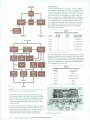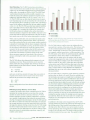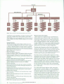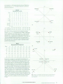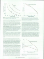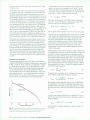
1
H E W L E T - P A C K A R D JOURNAL February 1996 HEWLETT> PACKARD © Copr. 1949-1998 Hewlett-Packard Co. In M e m o r i a m On November 23, 1995, Hewlett-Packard lost a close friend and a consistent source of inspiration with the death of Barney Oliver. Barney was a towering figure in HP's his tory, founded he was especially close to HP Laboratories, the organization he founded and directed for almost 25 years. Some of his technical contributions were described in more than a dozen HP Journal articles. But his technical achievements were just part of the legacy he leaves. No one who ever worked with or knew Barney can forget his insistence on excellence and innovation. He was a great intellect and a master inven tor whose interests and expertise spanned many scientific disciplines. He will be deeply missed. February 1996 Hewlett-Packard Journal 3 © Copr. 1949-1998 Hewlett-Packard Co. H E W L ETT-PA C K A R D JOURNAL February 1996 Volume 47 • Number 1 Articles ! Symmetric Multiprocessing Workstations and Servers System-Designed for High Performance and Low Cost, by Matt J. Marline, Brendan A. Voge, Loren P. Staley, and B adir M. Mousa j K-Class Power System | A High-Performance, Low-Cost Multiprocessor Bus for Workstations and Midrange Servers, by Will/am R. Bryg, Kenneth K. Chan, and Nicholas S. Fiduccia // Runway Bus Electrical Design Considerations 25 Design Gordon the HP PA 7200 CPU, by Kenneth K. Chan, Cyrus C. Hay, John R. Keller, Gordon P. Kurpanek, Francis X, Schumacher, and Jason Zheng 34 Verification, Characterization, and Debugging of the HP PA 7200 Processor, by Thomas B. Alexander, Kent A. Dickey, David N. Goldberg, Ross V. La Fetra, James R. McGee, Nazeem Noordeen, and Akshya Prakash 44 A New Memory System Design for Commercial and Technical Computing Products, by Thomas H. Hotchkiss, Norman D. Marschke, and Richard M. McClosky 52 Hardware Cache Coherent Input/Output, by Todd J. Kjos, Helen Nusbaum, Michael K. Traynor, and Brendan A. Voge Executive Robin Steve Beitler • Managing Editor, Charles L Leath « Senior Editor, Richard P. Dolan • Assistant Editor, Robin Everest Publication Production Manager, Susan E. Wright • Illustration, Renee D. Pighini • Typography/Layout, John Nicoara Advisory Thomas Rajeev Badyal, Integrated Circuit Business Division, Fort Collins, Colorado • Thomas Beecher, Open Systems Software Division, Chelmsford, Massachusenes • Steven Brittenham, Disk Memory Division, Boise, Idaho • William W. Brown, Integrated Circuit Business Division, Santa Clara, California • Rajesh Desai, Commercial Systems Division, Cupertino, California • Kevin G. Ewert, Integrated Systems Division, Sunnyvale, California • Bernhard Division, Bòblingen Medical Division, Bòblingen, Germany Douglas Gennetten, Greeley Hardcopy Division, Greeley, Colorado* Gary Gordon, HP Laboratories, Palo Alto, California Mark Gorzynski, InkJet Supplies Business Unit, Corvallis, Oregon • Matt J. Marline, Systems Technology Division, Roseville, Division, • Kiyoyasu Hiwada, Hachioji Semiconductor Test Division, Tokyo, Japan* Bryan Hoog, Lake Stevens Instrument Division, Everett, Washington Division, C. Steven Joiner, Optical Communication Division, San Jose, California • Roger L Jungerman, Microwave Technology Division, Santa Rosa, California Cupertino, California Kellert, Microwave Technology Division, Santa Rosa, California • Ruby B. Lee, Networked Systems Group, Cupertino, California • Swee Kwang Lim, Andrew Peripherals Division, Singapore • Alfred Maute, Waldbronn Analytical Division, Waldbronn, Germany Andrew McLean, Enterprise Messaging California Pinewood, England • Dona L Miller, Worldwide Customer Support Division, Mountain View, California • Mitchell Mlinar, HP-EEsof Division, Westlake Village, California • Michael P. Moore, VXI Systems Division, ioveland, Colorado • Shelley I. Moore, San Diego Printer Division, San Diego, California • M. Shahid Mujtaba, HP Laboratories, Palo Alto, California • Steven J. Narciso, VXà Systems Division, Loveland, Colorado • Danny J. Oldfield, California Measurements Division, Colorado Springs, Colorado • Garry Orsolini, Software Technology Division, Roseville, California • Ken Poulton, HP Sabatella, Palo Alto, California • Giinter Riefaesell, Bòblingen Instruments Division, Bòblingen, Germany • Marc Sabatella, Software Engineering Systems Division, Fort Collins, Colorado • Michael B. Saunders, Integrated Circuit Business Division, Corvallis, Oregon • Philip Stenton, HP Laboratories Bristol, Bristol, England Stephen R. Undy, Systems Technology Division, Fort Col/ins, Colorado • Jim Willits, Network and System Management Division, Fort Collins, Colorado • Koichi Yanagawa, Kobe Instrument Division, Kobe, Japan • Dennis C. York, Corvallis Division, Corvallis, Oregon • Barbara Zimmer, Corporate Engineering, Palo Alto, California The Hewlett-Packard Journal is printed on recycled paper. ©Hewlett-Packard Company 1996 Printed in U.S.A. February 1996 Hewlett-Packard Journal © Copr. 1949-1998 Hewlett-Packard Co. ] A 1.0625-Gbit/s Fibre Channel Chipset with Laser Driver, by Justin S. Chang, Richard Dugan, Benny W.H. Lai, and Margaret M. Nakamoto I Applying the Code Inspection Process to Hardware Descriptions, by Joseph J. Gilray I Overview of Code-Domain Power, Timing, and Phase Measurements, by Raymond A. Birgenheier Departments 5 7 7 94 In this Issue Cover What's Ahead Authors The Hewlett-Packard Journal is published bimonthly by the Hewlett-Packard Company to recognize technical contributions made by Hewlett-Packard (HP) personnel. While the information found in this publication is believed to be accurate, the Hewlett-Packard Company disclaims all warranties of merchantability and fitness for a particular purpose and all obligations and liabilities for damages, including but not limited to indirect, special, or consequential damages, attorney's and expert's fees, and court costs, arising out of or in connection with this publication. Subscriptions: The Hewlett-Packard Journal is distributed free of charge to HP research, design and manufacturing engineering personnel, as well as to qualified non-HP individuals, libraries, and educational institutions. To receive an HP employee subscription you can send an email message indicating your HP entity the mailstop to [email protected]. hp.com. Qualified non-HP individuals, libraries, and educational institutions in the U.S. can request 94304, an by either writing to: Distribution Manager, HP Journal, M/S 20BH, 3000 Hanover Street, Palo Alto, CA 94304, or sending an email message to: hp_journal@hp-paloalto-gen13. om.hp.com. When submitting an address change, please send a copy of your old label to the address on the back by Manager, subscriptions can be requested by writing to the HP headquarters office in your country or to Distribution Manager, address above. Free subscriptions may not be available in all countries. The Hewlett-Packard Journal is available online via the World-Wide Web (WWW) and can be viewed and printed with Mosaic and a postscript viewer, or downloaded http://www.hp.com/ a hard drive and printed to a postscript printer. The uniform resource locator (URL) for the Hewlett-Packard Journal is http://www.hp.com/ hpj/Journal.html. Submissions: with articles in the Hewlett-Packard Journal are primarily authored by HP employees, articles f rom non-HP authors dealing with HP-related contact or solutions to technical problems made possible by using HP equipment are also considered for publication. Please contact the Editor before articles such articles. Also, the Hewlett-Packard Journal encourages technical discussions of the topics presented in recent articles and may are letters expected to be of interest to readers. Letters should be brief, and are subject to editing by HP. Copyright publication 1996 Hewlett-Packard Company. All rights reserved. Permission to copy without fee all or part of this publication is hereby granted provided that 1 ) advantage; Company are not made, used, displayed, or distributed for commercial advantage; 2) the Hewlett-Packard Company copyright notice and the title of the stating and date appear on the copies; and 3) a notice appears stating that the copying is by permission of the Hewlett-Packard Company. Please Journal, inquiries, submissions, and requests to: Editor, Hewlett-Packard Journal, M/S 20BH, 3000 Hanover Street, Palo Alto, CA 94304 U.S.A. February 1996 Hewlett-Packard, Journal © Copr. 1949-1998 Hewlett-Packard Co. In this Issue Symmetric multiprocessing means that a system can distribute its workload evenly and multiple CPUs. Thus, coupled with high-performance memory and I/O subsystems, a symmetric multiprocessing system is able to provide ualdiiuau high performance. The article on page 8 begins a group of articles that describe a new servers of symmetric multiprocessing workstations and servers that have both customer cost and high performance and satisfy a wide range of customer needs. First, there are the HP 9000 J-class high-end workstations and the HP 9000 K-class servers, which run the HP-UX operating system, and then there are the system. 3000 Series 9x9KS servers, which run the MPE/iX operating system. The J-class workstation provides up to two-way symmetric multiprocessing, and the K-class server provides up to four-way symmetric multiprocessing. These systems are based on the superscalar PA-RISC processor called the PA 7200 (page 25) and a high-speed memory bus called the Runway bus (page 18). The Runway bus, which is the backbone of these J/K-class platforms, is a new processor-to-memoryand-l/0 multiprocessing that is ideally suited for for one-way to four-way symmetric multiprocessing for high-end workstations and midrange servers. The bus includes a synchronous, 64-bit, split-transaction, time multiplexed address and data bus that is capable of sustained memory bandwidths of up to 768 Mbytes per second in a four-way system. One of the PA goals for the Runway bus was to support the PA 7200 and future processors. The PA 7200 superscalar CPU evolution of the high-performance, single-chip superscalar PA 7100 CPU design. The processor and the Runway bus are designed for a bus frequency of 120 MHz in a four-way multiprocessor system, which mentioned the sustained memory bandwidth of 768 Mbytes per second mentioned above. The PA 7200 multiprocessor all the circuits required for one processor in a multiprocessor system except for external cache arrays. Among some of the features contained in the PA 7200 are a new data cache organization, a prefetching mechanism, and two integer ALUs for general integer superscalar execution. The PA 7200 is described on page 25 . The increased functionality and higher operating frequency of today's VLSI chips have created a corre sponding increase in the complexity of the verification process. In fact, chip verification activities now consume and time and resources than design. The article on page 34 describes the functional and electrical verification process used for the PA 7200 processor to ensure its quality and correctness. Since the early of the PA 7200 was based on the PA 7100 processor, verification could begin very early in the design because the same modeling language and simulator used for the PA 7100 could be used for the PA and The article also describes debugging activities performed and the testability features pro vided on the PA 7200. After investigating ways to improve customer application performance by observing existing platforms, the HP 9000 J/K-class design team determined that memory capacity, memory bandwidth, memory latency, parallel) system-level parallelism (multiple CPUs and I/O devices all accessing memory in parallel) were key elements in achieving high performance. As the article on page 44 describes, a major improve ment parallelism interleaving, bandwidth was achieved through system-level parallelism and memory interleaving, which were designed into the Runway bus and the J/K-class memory subsystem. Cache coherency refers to the consistency of data between processors (and associated caches), memory modules, and I/O devices. For the HP 9000 J/K-class systems, a scheme called hardware cache coherent I/O was introduced. This technique involves the I/O system hardware in ensuring cache coherency, thereby reducing memory and processor overhead and contributing to greater system performance. Cache coherent I/O is discussed in the article on page 52. The articles on pages 60 and 68 are more papers from the proceedings of HP's 1995 Design Technology Conference (DTC). The first article describes a 1.0625-Gbit/s Fibre Channel transmitter and receiver chipset. About two-chip, years ago HP introduced the first commercially available, two-chip, 1.4-gigabit-per-second, low-cost, serial data link interface, the HP HDMP G-link chipset. The new chipset, the HP HDMP-1512 6 February 1996 Hewlett-Packard Journal © Copr. 1949-1998 Hewlett-Packard Co. (transmitter) and the HP HDMP-1514 (receiver) are a low-cost gigabit solution for Fibre Channel applica tions. specification The implements the Fibre Channel FC-0 physical layer specification at 1.0625 Gbits/s. The transmitter features 20:1 data multiplexing with a comma character generator and a clock synthesis phase-locked loop, and includes a laser driver and a fault monitor for safety. The receiver performs clock recovery, 1:20 data demultiplexing, comma character detection, word alignment, and redundant loss-of-signal alarms for eye safety. The other for paper (page 68) discusses using the traditional software code inspection process for inspecting hardware descriptions written in Verilog HDL (hardware description language). The code inspection process for software development has been around for awhile and has proven itself to be an effective tool for finding design and code defects and sharing best practices among software engineers. The authors found that except for some issues specific to HDL, the format and results of their inspection process were very similar to the standard software inspection process. The Telecommunications Industry Association (TIA) has released two standards (IS-95 and IS-97) that specify (code various measurements required to ensure the compatibility of North American CDMA (code division tele access) cellular transmitters and receivers. CDMA, which is used by the cellular tele phone to is a class of modulation that uses specialized codes to provide multiple communication channels a a designated segment of the electromagnetic spectrum. The article on page 73 provides a tutorial overview of the operation of the algorithms in the HP83203B CDMA cellular adapter, which is designed covers make the base station measurements specified in the TIA standards. The article also covers the general concepts of CDMA signals and measurement and some typical measurements made with theHP83203B. C.L Leath Managing Editor Cover The HP 9000 J/K-class servers and workstations and the HP 3000 Series 9x9KS servers are system-de signed design high performance and low cost, meaning that all of the boards have design features that opti mize their functionality specifically for these systems. The cover is a group photograph of the boards. Individual descriptions and photos can be found in the article on page 8. What's Ahead Articles for for the April issue include eight articles on the Common Desktop Environment (CDE) for systems system, on the UNIX'® operating system and articles on the PalmVue mobile patient data system, the HP G1009A protein analyzer, and a power module for cellulartelephones. February 199fi Hewlett-Packard Journal 7 © Copr. 1949-1998 Hewlett-Packard Co. Symmetric Multiprocessing Workstations and Servers System-Designed for High Performance and Low Cost A new system of workstations and servers provides enhanced system performance in several price classes. The HP 9000 Series 700 J-class workstations provide up to 2-way symmetric multiprocessing, while the HP 9000 Series 800 K-class servers (technical servers, file servers) and HP 3000 Series 9x9KS business-oriented systems provide up to 4-way symmetric multiprocessing. by Matt J. Harline, Brendan A. Voge, Loren P. Staley, and Badir M. Mousa I/O bandwidth between 128 Mbytes/s and 160 Mbytes per second (95 to 116 Mbytes/s peak sustained bandwidth). The HP-HSC bus is an extension of the GSC (General System Connect) bus used in earlier workstations.1 Blending high performance and low cost, a new family of workstations and servers has been designed to help main tain HP's leadership in system performance, price/perfor mance, system support, and system reliability. This article and the accompanying articles in this issue describe the design and implementation of the HP 9000 J-class work stations, which are high-end workstations running the HP-UX operating system, the HP 9000 K-class servers, which are a family of midrange technical and business serv ers running the HP-UX operating system, and the HP 3000 Series 9x9KS servers, which are a family of midrange busi ness servers running the MPE/iX operating system. In this issue, these systems will be referred to collectively as J/Kclass systems. In addition to the Runway and HP-HSC buses, the J/K-class systems also support a connectivity I/O bus. In the HP 9000 J-class workstation systems, the connectivity I/O bus is EISA (Extended Industry Standard Architecture); it has a peak bandwidth of 32 Mbytes/s. In the HP 9000 K-class and HP 3000 Series 9x9KS server systems, the connectivity I/O bus is the HP Precision Bus (HP-PB). The servers have one or two four-slot HP-PB adapters. Each HP-PB has a peak bandwidth of 32 Mbytes/s. The goals of the the design team were to achieve high per formance and low cost, while at the same time creating a broad family of systems that would share many of the same components and meet a wide range of customer needs. The challenge was to create a list of requirements that would meet the needs of the three different target markets: the UNIX®-system-based workstation market, the UNIX-systembased server market, and Hewlett-Packard's proprietary MPE/iX-system-based server market. The basic require ments for these systems were to deliver leadership symmet ric multiprocessing performance, memory performance, and capacity, along with exceptional I/O performance. Balanced system performance was the overall goal. Processor The core of the J/K-class systems is a high-performance pro cessor module that interfaces directly to the Runway bus. It is based on the HP PA 7200 CPU chip,2 a PA-RISC super scalar processor, which is an evolution of the high-perfor mance, single-chip, superscalar PA 7100 processor. The PA 7200 incorporates a high-speed Runway bus interface, a new data cache organization with an on-chip assist cache, data prefetching, and two integer ALUs. This microprocessor is fabricated using HP's 0.55-micrometer CMOS process and delivers reliable performance up to 120 MHz. More informa tion on the PA 7200 can be found in the article on page 25. Fig. 2 is a photograph of the processor module. Hardware Features All of the J/K-class platforms are built around the same basic building blocks (see Fig. 1). The backbone of these systems is the high-speed processor-memory bus called the Runway bus. This is a 640-to-768-Mbyte/s (peak sustained bandwidth), 64-bit-wide bus that connects the processors, system main memory, and the I/O adapter (bus converter). The Runway bus is described in more detail in the article on page 18. The I/O adapter provides connections to two HP-HSC (HewlettPackard high-speed system connect) buses, providing a raw The tables on page 10 indicate the processor speeds for each of the platforms in the J/K-class family. Table I is for the HP-UX workstation systems, Table II is for the HP-UX symmetric multiprocessing servers, and Table III is for the MPE/iX symmetric multiprocessing servers. System Board Central to the J/K-class systems is the system circuit board (Fig. 3). This printed circuit board contains all the circuitry required for implementing the Runway bus and connectors 8 February 1996 Hewlett-Packard Journal © Copr. 1949-1998 Hewlett-Packard Co. System Power Monitor I Power Supply I = Instruction D = Data MMC= Master Memory Controller SMC = Slave Memory Controller DM = Data Multiplexer IOA = I/O Adapter PDH = Processor Dependent Hardware PDC = Processor Dependent Code HSC = High-Speed System Connect Memory Carrier System Board HP-HSCBus HP-HSCBus HP-HSC/ I SCSI H P - P B B u s Adapter II Adapter Core I/O • Expansion Controller • Slot HP-Precision Bus (HP-PB) Console Access Port MUXand Modem Fast/Wide SCSI Peripheral Bay H-t-fr Fast/Wide SCSI I I I Single-Ended SCSI Local Console Port I Other MUX Ports PA7200 CPU with Heat Sink Cache RAMs Fig. 2. Processor module. Cache RAMs Panel Port IEEE 802.3 Port| Remote Console Port Fast/Wide SCSI Mouse Keyboard Fig. 1. Block diagram of the HP 9000 Model K400 server. for the processors, the master memory controller, and the I/O adapter. The bootstrap code and other system-specific hardware are also on the system board. For the entire family of J/K-class systems, there are only three system board de signs: one for the 1-way or 2-way symmetric multiprocessing workstation configuration (J class), one for the uniproces sor server configuration (K 100), and one for the 1-way to 4-way symmetric multiprocessing server systems (K2xO, K4xO). In the workstation systems, the system board includes the Runway bus and system dependent hardware mentioned above, the complete memory system including the connec tors for the memory modules (SIMMs), most of the circuitry required for the system's built-in I/O functionality (core I/O), and power supply management and control circuits. Five I/O slots are provided for system I/O expansion. These five slots are shared; a combination of EISA and HP-HSC cards can be installed, with a maximum of four EISA cards or three HPHSC cards. For example, a system could have four EISA February 1996 Hewlett-Packard Journal 9 © Copr. 1949-1998 Hewlett-Packard Co. Similarly, processors that fail self-test are deconfigured and the system boot process is continued. Table I HP 9000 J-Class Processor Speeds P r o c e s s o r Model S l o t s J 2 0 0 J 2 1 2 0 S p e e d 1 0 0 1 2 P r o c e s s o r 0 M H z M H z Table II HP 9000 K-Class Processor Speeds In addition to providing a robust system to the customer, the system firmware allows designers and the manufacturing processes easy access to system test and configuration of hardware and firmware features. Some of these features allow enabling or disabling of processor cache pref etching, full memory test or memory initialization only, and so on. This helped in the system debug effort by speeding the boot process and making it possible to disable certain functions while searching for the root cause of a bug in the system. Another feature built into the system firmware during the system debug process was a debug interface that would allow the lab engineers to set soft breakpoints and step through instruction execution one instruction at a time. This tool proved to be quite valuable, providing increased visibility into system behavior and the system state. Table III HP 3000 Series 9x9KS Processor Speeds Series P r o c e s s o r S l o t s P r o c e s s o r S p e e d 9 3 9 K S 1 8 0 M H z t 9 5 9 K S 4 1 0 0 M H z 9 6 9 K S 4 1 2 0 M H z The J/K-class firmware is installed in flash EPROM. The firmware can be updated through the system offline diag nostic environment. If for any reason the system firmware needs to be modified, it can easily be upgraded by loading a new firmware image from tape or another medium into system memory and then loading it into the firmware flash EPROM. The result of these design choices is system firmware that provides flexible functionality, reliable system test and ini tialization, and some tolerance for certain types of failed components in the system boot process. High-Performance Memory t Effective Processor Speed cards and one HP-HSC card, or three EISA and two HP-HSC cards, or two EISA and three HP-HSC cards. The symmetric multiprocessing server system board in cludes the Runway bus and system dependent hardware as described above, along with slots for a separate core I/O card, an optional expansion HP-HSC I/O carrier card, one or two IG-byte memory carriers, and four or eight HP-PB slots. Four Runway slots are provided for the processor modules. Depending on the processor used in the system, the Runway bus operates at 100 MHz or 120 MHz. Memory performance was highly important throughout the J/K-class system design and implementation. The J/K-class memory subsystem is designed with consideration for high bandwidth, low latency, and expandability from 32M bytes Dual I/O Adapter The uniprocessor system board (HP 9000 Model K100) has a single processor, all memory controllers and SIMM slots, a core I/O card slot, and four HP-PB slots. System Firmware All of the J/K-class systems share a common firmware base that tests and initializes the system on power-up. This code is a combination of PA-RISC assembly code and C. It was a design goal to support all of the server products using the same firmware and to have a common firmware base for the technical workstation products. The code was designed in a very modular fashion so that the code base could be easily ported to the various system platforms. The system firmware is designed to be very robust. For ex ample, during memory configuration and test, it uses a com bination of bank and page deallocation to deconfigure mem ory containing hard errors, allowing the user to continue using the system until the failing memory can be replaced. 8 HP-PB I/O Slots Fig. 3. System board. 10 February 1996 Hewlett-Packard Journal © Copr. 1949-1998 Hewlett-Packard Co. Expansion HP-HSC I/O Master Memory Controller to 2G bytes. It is capable of interleaving memory accesses across 32 banks of memory. The memory system is built around the master memory controller (MMC). which inter faces to the high-speed Runway bus. The MMC communi cates with up to eight slave memory controllers (SMC) on one or two memory carriers (see Fig. 4 and the article on page 44). Also on the memory carriers are data multiplexers and pairs of SIMMs (single-inline memory modules). This design results in a high-bandwidth, interleaved. 2G-byte memory subsystem. As 64M-bit DRAMs become costeffective, the 2G-byte limit will increase to 3.75G bytes of main memory. Table IV shows the maximum amounts of memory available in various J/K-class systems. Supporting a high-density and high-performance memory system with industry-standard memory SIMMs would have resulted in a costly memory system that would not have performed at the desired levels. Instead of the industrystandard approach, a denser memory module was designed. These memory modules (Fig. 5) are actually a dual-inline design, although they are still referred to as SIMMs. In the J/K-class systems, these dual SIMMs are inserted in pairs, providing two separately addressable, 128-bit, ECC (error correcting code) protected banks of memory (144 bits including ECC check bits). Each dual SIMM provides 72 bits of the two 144-bit banks. Using 4M-bit or IGM-bit DRAMs, the SIMMs are available in 16M-byte and 64M-byte sizes. While these memory modules are not standard, there is no HP proprietary technology in them, helping to keep memory pricing very competitive with the industry. I/O Adapter The J/K-class I/O adapter (bus converter) interfaces between the Runway bus and the HP-HSC I/O bus. The I/O require ments for a J/K-class system call for multiple I/O buses, so the I/O adapter package contains two fully independent bus Slave Memory Controllers SIMM Slots Fig. 4. Memory carrier board. DHtnMUX SIMM Slots Fig. 5. Dual-inline memory module. converters (see Fig. 6a). To maximize system flexibility, the I/O adapter is designed to support a range of bus frequen cies on either bus, thus requiring a full synchronizer. Fig. 6b is a block diagram of the I/O adapter. The HP-HSC bus only has a 32-bit address space, while the Runway bus supports a 40-bit address space. This requires an address translation mechanism to provide the additional eight address bits. The processor's aggressive data prefetching requires a new mechanism for DMA (direct memory access) to coexist with this processor feature. Hardware cache coherent I/O solves these two problems (see article, page 52). Prefetching is also included in the HP-HSC bus to reduce memory read latency and increase I/O bandwidth. All of these features required additional hardware support in the I/O adapter. According to the PA-RISC architecture definition, a bus con verter also needs to provide the registers to configure address space, enable and disable features, log errors, manipulate the TLB, and provide diagnostic access. Therefore, these registers are included in the I/O adapter. The J/K-class systems required several other hardware fea tures that by default were put into the I/O adapter. Among these is the hardware to interface to external components implementing the processor dependent hardware (PDH) necessary to provide boot firmware, stable storage for system configuration information and error logging, and scratch RAM. The I/O adapter also provides a real-time clock for keeping track of time when power is off. Basic VLSI support of scan-based testing, both internal and boundary (JTAG or IEEE 1149.1), is built into the I/O adapter, along with double-strobe capability for speed path testing and built-in self-test (BIST) for the RAM structures. Finally, it was desired that the design be done in a modular fashion, enabling future designs to easily borrow portions of the design for future enhancements or to lower costs. This required that the chip be designed with well-defined and simple interfaces. The synchronizers made very natural places to define the boundaries of these modules. All of these requirements led to a modular, synchronizer queuecoupled, hardware cache coherent, dual bus converter design. Core I/O Functionality The basic I/O requirements for both the workstation and the server systems include 20-Mbyte/s fast-wide SCSI (Small Computer System Interface) for system disk connectivity, 5-Mbyte/s single-ended SCSI for archival storage, and an IEEE 802.3 LAN interface for networking. The HP-UX February 1996 Hewlett-Packard Journal 1 1 © Copr. 1949-1998 Hewlett-Packard Co. Runway Bus I/O Adapter (Bus Converter ) A I/O Expansion I/O Adapter (Bus Converter ) B ^•H On the HP 9000 K-class server systems, several configura tions support various system I/O needs (see Table V). As a minimum, the system comes with one 32-MHz HP-HSC bus slot for expansion I/O. This slot is in a compact 3-by-5-inch form factor. As I/O needs increase, the system can be up graded to provide four 40-MHz HP-HSC slots in addition to the one 32-MHz HP-HSC slot (Model K4xO only). In addition to the HP-HSC slots, the K-class server has four or eight Hewlett-Packard Precision Bus (HP-PB) slots. These slots are configured such that the user can install up to four double-high HP-PB cards and still have four single-high HP-PB card slots available. Processor Dependent Hardware Port Table V HP 9000 K-Class I/O Expansion Capabilities HP-HSC Bus Porti HP-HSC Bus Port 2 Runway Buffers f I Runway Receive Register Pool (Outstanding Read Transactions and Prefetch Data) Runway Drive Register t Combined bandwidth of the two HP-HSC buses. O u t b o u n d C a c h e Queues Coherency (Synchronizer) I Queues Inbound Queues (Synchronizer) In the HP 9000 J-class workstation configurations, the system supports an 8-MHz EISA bus (maximum of four slots) and a 40-MHz HP-HSC expansion I/O bus (maximum of three slots). These slots provide the workstation user with a great deal of flexibility in configuring I/O devices and meeting high-speed I/O requirements (see Table VI). Table VI HP 9000 Model J2xO I/O Expansion Capabilities I / O Processor Dependent Hardware Port HP-HSC Receive TLB Control Register S l o t S l o t C o n f i g u r a t i o n 0 H P - H S C Slot 1 HP-HSC or EISA M H Slot 2 HP-HSC or EISA PDH Port Ib) T S l o t 3 E I S A S l o t 4 E I S A HP-HSC Local /Console Fig. I/O (a) There are two fully independent I/O adapters in the I/O adapter package, (b) I/O adapter block diagram. systems also include a Bitronics parallel interface port, keyboard and mouse connections, and serial I/O ports as part of the core I/O functionality. A photograph of the Kclass core I/O board is shown in Fig. 7. The workstation model adds high-quality audio input and output to the built-in core I/O. The server system includes additional serial ports and an integrated modem for remote service access. The server systems also have a remote service console access port to allow remote servicing of hardware and software by Hewlett-Packard's customer support organizations. Mouse Fig. 7. K-class core I/O board. 1 2 February 1996 Hewlett-Packard Journal © Copr. 1949-1998 Hewlett-Packard Co. A number of I/O cards are currently available for use in the high-speed I/O and HP-PB bus slots. A number of EISA cards are supported in the workstation system. The following is a partial list of the I/O cards available for J/K-class systems: • 5-Mbyte/s single-ended SCSI • 20-Mbyte/s fast-wide SCSI • HP Fiber Link • IEEE 802.3 LAX • IEEE 802.5 token ring •FDDI • FibreChannel • ATM (asynchronous transfer mode) • Programmable serial interface • Bitronics parallel port • 16-port serial RS-232 • 32-port serial RS-232 • 2D graphics card • 3D graphics card. their up- in ease of installation, serviceability, and field upgradability. The labels use color coding and detailed diagrams clearly defining such things as board locations, memory SLMM loading sequences, and disk locations. These have been very successful in making the many configurations easily understood by customers and HP manufacturing and field service personnel. Server Package Design Like every other aspect of the design of the J/K-class sys tems, designing the chassis and plastics proved to be chal lenging. With a strong emphasis on development schedule and a desire for a very robust and flexible design, the engi neering team had to create some innovative solutions to keep on schedule and keep the cost of the product low. Several requirements defined the maximum height and width of the server box. It had to fit into a 19-inch rack, so it could be no wider than 17.3 inches and no deeper than 25 Integrated Peripherals The server systems all have a standard DDS tape drive and a CD-ROM drive integrated into the system. In addition, there is space available for up to four 20-Mbyte/s SCSI disk drives in the system box. The workstation comes with a standard 3.5-inch flexible disk drive, a CD-ROM drive, a tape drive, and two slots for 20-Mbyte/s SCSI disk drives built into the system box. Industrial Design The J/K-class industrial design is intended to convey a strong perception of the power within, wrapped in bold, distinctive designs that are elegant and pleasing to the eye. The K-class product is designed to work as a floor-standing product as well as rack-mounted in an industry-standard HP 19-inch EIA rack (Fig. 8). A growing number of rack-mounted HP peripheral products such as disk arrays, uninterruptible power supplies, and LAN hubs complement the overall sys tem. The J-class system (Fig. 9) is designed for floor-standing use in the commercial workstation environment, but can be rack-mounted on a custom basis. These machines were designed with ease of assembly and serviceability as high priorities. They use plastic parts that snap together over a riveted steel chassis without a single screw or fastener, making assembly and disassembly very quick and easy for service and for the eventual recycling at the end of the products' life. Customer ease of use was another design priority. This is evident in the brightly backlit liquid crystal display, which conveys system status information in a clear text font, a vast improvement over previous systems, which had flashing LEDs. A simple three-position keyswitch for on, off, and service mode is clearly marked and positioned within easy reach on the front of the K-class system. The front door gives the user easy access to peripherals and visual feedback in the form of disk activity lights. Inside the front door are a pocket for the user manual, a safe storage location for the system key, and a system label with the most pertinent user information. Extensive effort went into label design, working with field support engineers, to make these products the leaders in Fig. 8. K-class server configurations. February 1996 Hewlett-Packard Journal 13 © Copr. 1949-1998 Hewlett-Packard Co. power monitor, and the uninterruptible power supply (UPS). The power features implemented in the workstation and server systems are slightly different but follow the same general philosophy: provide reliable power to the system at a low cost. The server system power supply provides the voltage rails for the components in the system. This 925-watt supply in corporates power factor correction and accepts a wide range of input voltages and input frequencies between 50 and 60 Hz. It provides a carryover time of 20 milliseconds after a power failure. The system power supply does not include any intelligence to control the system turn-on or reset activities. This intelli gence is provided by the system power monitor (Fig. 10). This circuit monitors the various aspects of the computer system and the power supply output to determine if the power should be turned on or off. This includes monitoring the system internal temperature, checking the voltage out put to ensure that there is no undervoltage or overvoltage condition, and providing diagnostic messages on the system's liquid crystal display when problems occur. Fig. 9. J-class workstation system processing unit. inches. It could be no taller than 25.24 inches, so that as a standalone unit it would fit under a standard table. An additional challenge was that of the Runway bus. The expected high speeds of the bus required that the bus length be kept to a minimum to reduce signal propagation delays. At the same time, up to six different components needed to attach to this bus: four processors, the master memory con troller (MMC), and the I/O adapter. The processor module spacing was kept to 1.2 inches, allowing the overall length of the Runway bus to be short enough to support reliable 120-MHz operation. This small size also presented an additional challenge, that of cooling the many components in the system. An intensive effort was launched to simulate and create mockups of the proposed mechanical designs for airflow and expected inter nal system temperature rises. A number of cooling alterna tives were proposed and evaluated. The resulting solution provides an air-cooled system with excellent airflow and a remarkably quiet system for the power dissipated within the box. There are only two fans in the entire system. The uninterruptible power supply (UPS) is an optional com ponent of the J/K-class systems. It provides additional assur ance of system availability and data integrity, even if the ac power lines fail for any reason. Upon a powerfail event, the UPS provides ac power to the system for up to 15 minutes, allowing the system to continue operation, or in the case of an extended power outage, to shut down gracefully and save critical data to disk. When ac power returns, the system will continue operation, or if it was shut down, it can be restarted without loss of data. More details on the power supply, monitor, and UPS can be found on page 16. System Performance The J/K-class systems were developed to provide customers with excellent performance in the intended markets: midrange servers and high-end workstations. Our goal was not necessarily to provide the highest single-component perfor mance, but to provide customer-valued application perfor mance at an extremely attractive price. Other desired features helped to define how the system was partitioned into the various circuit boards. Each board needed to be easy to access. Almost every component in the system can be accessed and removed from the system for maintenance or repair in a matter of minutes. The size and type of add-on I/O cards also required some creative design to allow flexibility in the design as well as flexibility for the customer. Power System The power system for the J/K-class systems can be split into three subsystems: the system power supply, the system Fig. 10. System power monitor. 14 February 1996 Hewlett-Packard Journal © Copr. 1949-1998 Hewlett-Packard Co. The most common component benchmark is the SPEC (Systems Performance Evaluation Cooperative) suite, which measures CPU integer and floating-point performance. For these benchmarks, the processor in the J/K-class products provides about 168 SPECint92 integer and 258 SPECfp92 floating-point performance at 120 MHz. With the wellbalanced symmetric multiprocessing J/K-class systems, the SPECrate_int performance of a four-processor 120-MHz system is 12,150 and the SPECrate_fp92 performance is 19,600. It is in the real-world applications and at the system level where the J/K-class computer systems really start to shine. The balanced design of the Runway processor-memory bus, the memory subsystem, and the performance I/O system provides the user with exceptional performance. Two widely used benchmarks that try to measure the performance of realistic customer workloads are SPEC SFS1.0(LADDIS) and TPC-C. The 120-MHz LADDIS performance of the J/Kclass is as high as 4750 I/O operations per second, which exceeds many high-end servers that typically have twice as many processors (8 to 10 processors compared to four for a Model K400). A four-way J/K-class server at 120 MHz has demonstrated in excess of 3,000 transactions per minute on the TPC-C transaction benchmark. At the time of introduc tion of the J/K-class systems, the only other single system with higher performance was HP's own T500 corporate business server. On the technical side, workstation applications clearly bene fit from the increased memory bandwidth. At the same time, the introduction of multiprocessing in a high-end client configuration provides the opportunity for either parallel processing of a single task or more parallel execution for multiple tasks. With the addition of the new high-end HP Visualize48 graphics, for which the J-class systems provide some specific hardware performance enhancers, the work station products will handle large, complex design and visualization problems easily. Design for Lasting Value The J/K-class systems were designed to provide HP's custom ers with lasting value. Processors can be easily added to the system, to a maximum of two processors in the workstation systems and up to four processors in the server systems. Upgrading from 100-MHz to 120-MHz processors is just as simple. The J/K-class systems are also designed to accept future processors easily, such as the PA 8000 processor,3 through a simple processor module upgrade. Not only are processors easy to upgrade, but memory and I/O are also designed so that it is easy to add memory and I/O functionality. Memory can be added in 32M-byte or 128M-byte increments up to 1024M bytes in a J-class system or up to 2048M bytes in a K-class or Series 9x9KS system. As increased-density DRAMs become cost-effective, memory limits will increase to 3.75G bytes of main memory, filling most users' memory configuration and capacity requirements far into the future. System Verification The design of any computer system requires an extensive test and verification effort. For the chips and boards de signed for the J/K-class platforms, many engineer-months were dedicated to ensuring the systems manufactured and shipped to HP's customers are of the highest quality and reliability. This testing can be grouped into several different categories: presilicon chip and system simulation, formal verification methods, system functional verification, chip and system electrical characterization, and system validation. Simulation. Before committing any part of the J/K-class de sign to silicon, extensive simulation had already proven the basic functionality of each component individually and as part of the system. Each component design team provided a model of then- particular part of the design to an overall sys tem simulation team. The system simulation team then pulled together tools first to simulate subsystems and eventually to simulate the entire J/K-class system. In addition to the logical simulation to verify correct functionality, electrical simula tion was done for the critical portions of the system such as clock distribution, system buses, and chip internal critical paths (see article, page 34). Formal Methods. For some parts of any design, it is very diffi cult to verify complete adherence to design specifications. One area of concern in the J/K-class design was the bus pro tocols for the Runway bus. In an effort to reduce risk and improve system reliability, formal methods4 were used to analyze the bus transaction protocols used in the Runway bus definition. The analysis pointed to several defects, which were corrected before implementation of the system. Functional Verification. As the first components became avail able to the design teams for initial debugging, efforts were focused on verifying that each component functioned prop erly in the system. The first goal was to boot the system to the initial system loader. At this point either the operating system (HP-UX) could be loaded or system and component diagnostics could be loaded. While booting the operating system is a great accomplishment, the task of verifying cor rect functionality was far from completed when this was done. Numerous tests were developed specifically for the J/K-class systems. These tests employed a number of techniques for finding defective components and defects in design. These techniques included pseudorandom and pseudoexhaustive code and data sequences that stressed the processors (inte ger units, floating-point units, caches, program control, etc.), the memory and memory controllers, and the I/O bus adapters and I/O controller cards. Electrical Characterization. Once a minimal level of system functionality was attained, several electrical characteriza tion efforts were launched to prove that the components and the system would function in the electrical environ ment. This testing focused on measuring electrical noise on chips as well as boards, and looking at bus cross talk and power supply variation and noise. Systems were stressed beyond normal temperature ranges, voltage ranges, and fre quency ranges to find the weakest link in the system electri cal environment. Through all this characterization effort, designs were modified and improved, resulting in a system that is capable of running reliably throughout the specified system operating environment. System Validation. Because of the desire to stress the system beyond what HP's customers will do, the functional and February 1996 Hewlett-Packard Journal 15 © Copr. 1949-1998 Hewlett-Packard Co. K-Class Power System The power system in the HP 9000 K-class servers uses a number of new and emerging technologies to achieve excellent platform performance without com promising cost, reliability, and quality metrics. Combined in the power system are the system power monitor, the system power supply, and an optional uninterrupt ible monitor supply (UPS). Key contributions of the system power monitor include: system LCD and initialization including error reporting via a front-panel LCD display, temperature monitoring and cooling, fan speed control based on ambient temperature, fan synchronization and fault detection, continuous power supply output overtem- monitoring, special manufacturing modes of operation, overtemperatiirp detection and warning, overteniptiiaiure shutdown, and other features. The system power supply uses power factor correction to achieve low power-line distortion while maximizing the available VA capacity of the input ac circuit. A standard dc-to-dc forward converter follows the regulated power factor corrected output. Remote sensing is used on all output rails to achieve tight regulation specifications. The power system is optimized for use with several HP UPSs employing both offline and online technologies. The UPSs use an autoranging technology allowing worldwide use. Worldwide regulatory and safety approvals apply to these UPSs. The hardware provides power-line filtering and conditioning while both firmware provides many useful status and control capabilities, both real-time and programmed for later execution. To LCD System Logic Inputs System Power Monitor The system power monitor (Fig. 1 ) is where the power system gets its HP person ality. sys was intended that most if not all nonstandard features of the power sys tem would be concentrated in this assembly, as opposed to having them in the power microprocessor, itself. The power monitor is designed around a microprocessor, so that convenient of its features are determined by firmware. This made it convenient to modify without features as required during the system development phase, without changing hardware. The power monitor is powered by a dedicated +15Vdc supply which of turned nn at a!! times if the system has ac puwur. The functions of the power monitor are: • Check with CPU modules in the system to see that they are all compatible with each other. . Check CPUs power supply in the system to see that it is compatible with the CPUs present. • Respond to system keyswitch position and turn power supply on and off as required. • Monitor all power supply output voltages for valid range. • Monitor ambient temperature and initiate operator warnings. > Control fan speed as a function of ambient temperature. > Synchronize the two fans to avoid acoustic beating. • Check for fan failure. • Monitor internal system temperature for valid range. > Initiate system reset signals. > Issue ac powerfail warning signal. > In case of any system malfunction, shut down the system and write a message to the front-panel liquid crystal display indicating why the system was shut down. The notable contributions of the power monitor are its fan control scheme, which makes the system remarkably quiet for its power level, and its contribution to system maintainability through diagnostic display messages. System Logic Outputs Voltages Temperature Fan A Fan B Fig. 1. System power monitor block diagram. electrical characterization efforts mainly focused on test software and environments that do not match our custom ers' operating conditions. While it is likely that all hardware defects (design related as well as manufacturing related) will be found with the methods shown above, it is not known if the new hardware might uncover software defects. At the same time, it is possible that actual system software and applications could uncover hardware defects. For this reason, each system is tested under various load conditions and system configurations while running actual HP-UX and MPE/iX application programs and system exercisers. These efforts result in a system that has been designed to operate reliably in normal operating conditions a? well as under extremes of environment. System Power Supply The system power supply is rated for 925W of continuous dc output. Five output rails are provided: +3.30Vdc (VD|J, +4.4Vdc (VDH), +5.1Vdc (VUD), +12Vdc, and -12Vdc. The +3.3Vdc and +5.1 Vdc rails are used for standard logic circuits while the +4.4Vdc is used exclusively for the CPUs. The +1 2Vdc is used primarily for disk drives rails I/O with the remaining -12Vdc rail being used strictly for I/O. All rails have ±1 provided regulation windows. Additionally, a +15Vdc, 300-mA rail is provided for use by the system power monitor. This rail is electrically isolated from the computer rails. Its single point of ground is provided by the power monitor, which eliminates the potential for ground loops. The system power supply implementa tion is and entirely in discrete devices with one hybrid, four daughter cards, and a 2.6-mm-thick, HP FR4 motherboard. The density is 1 .8 watts per cubic inch. Both a discrete version and a dc-to-dc module approach were initially investigated, but cost, cooling, and reliability concerns ultimately resulted in the discrete version being chosen. Conclusion The J/K-class family of workstations and servers takes a big step in the direction of converging HP's workstation and server lines. At the same time, the J/K-class provides leader ship performance at exceptional value to computer systems users. Acknowledgments The authors wish to thank Scott Stallard, R&D lab manager at the beginning of the development of the J/K-class sys tems, as well as John Spofford, R&D lab manager during the final stages of testing and verification, for their support, 1 6 February 1996 Hewlett-Packard Journal © Copr. 1949-1998 Hewlett-Packard Co. The K-class power requirements required the maximum allowable VA capacity of a 100/1 require 15A branch circuit. To fully utilize the 15A circuit and not require customer installation of a 20A branch circuit it was decided early in the develop ment cycle that the system power supply would use power factor correction. This means that the input voltage and current waveforms are in phase, so the power supply traditional to be a resistive load on the ac line. By comparison, traditional offline switchers appear to the ac line as peak detectors and thus there are very large waveform. of input current at the peaks of the input voltage waveform. With the system power supply appearing resistive, power is drawn out of the ac line continuously rather than just at voltage peaks. Without power factor correction, typical offline switchers are limited to approximately 600W given 100Vac input lines. range factor correction also allows the supply to operate over a wide range of input voltages without requiring any additional circuitry such as autoranging circuitry or line select switches. The regulated output voltage of the power factor correction circuit ¡s +400Vdc. The supply is rated to operate with input voltages from 90Vac to 140Vac for its lower operating range and from 180Vac to 264Vac in its higher operating range. The frequency range of operation in either voltage range ¡s 50 to 60 Hz. There ¡s a minimum guaranteed carryover time of 20 ms before a powerfail warning is issued and an additional 5 ms of carryover time after correction that is issued. Another benefit of using power factor correction is that European norms for line distortion are already met when they become mandated in the European Community. Two forward dc-to-dc converters are employed in the power supply. Both convert ers take the regulated +400Vdc output of the power factor correction stage and convert it to the desired regulated output voltage. With the VQD rail exceeding 500W it made sense, considering component selection and cost, to have VQD generated by one converter and the remaining rails by a second converter which ¡s rated at about 425 watts. The use of two converters also allows sequencing of the Voo rail with respect to the VQH rail, which was a semiconductor requirement. Two output connectors are required for busing power between the power supply and the square board. The footprint of the connectors measures only six square inches, so the impact of the power system on the system board layout was minimal. Uninterruptible Power Supplies Unlike memory previous HP systems which used battery backup of only main memory during progress, duration ac power failures, thus halting any processes in progress, the K-class power supply uses uninterruptible power supplies (UPSs) for backup. This allows uninterrupted operation during an ac line failure for some predeter mined period of time after which the computer can be automatically and controllably shut down. Should the power be restored before shutdown ¡s required, processing will have continued uninterrupted. Should shutdown be required because of an extended power loss then the computer can do a controlled shut down controllable after which the UPS can be shut down. This controllable turn-off of the UPS and host computer is well-suited for applications in which customers want to reduce their energy consumption by shutting down equipment programmatically overnight or over the weekend. Two UPS technologies are available from HP. The lower-power units — 600VA (425W) standalone, 1300VAU300W) standalone, 1.3-kVA(1300W|rackmount.and 1.8-kVA (1800W) rackmount— all employ offline technology. The UPS directs the incoming ac directly to the load being supported unless the input falls outside of a defined set of voltage and frequency limits. Once this occurs the UPS then switches to inverter mode and outputs regulated ac using its internal batteries and a dc-to-ac upconverter. This technology is very effective, reliable, cost-competitive, and efficient for many applications in which a defined loss of ac input for the load can be supported. The time period during which there is no ac input is defined as transfer time. The offline units have a transfer time of 10 ms maximum and this maps well into HP's computer products which have a guaranteed carryover time of 20 ms minimum. The offline topology is very energy efficient; when the ac input ¡s within bat the UPS is just maintaining its internal batteries. Unless the bat teries in been run down because of an earlier power failure the batteries are in a "float" state and require very little input power. The topology employed by the high-power 3-kVA UPS is online interactive. In this technology the UPS monitors the incoming ac waveform and adjusts it on a cycleby-cycle basis, interactively regulating the output ac to the host computer system. Should transfers line deviate substantially outside of its normal range the UPS transfers from regulated to inverter mode and continues to provide the load with regulated ac derived from the UPS's internal batteries. This technology provides excellent regu lation of the ac output supplied to the load under all line conditions and is suitable for mission-critical applications where even slight losses of ac input are disruptive. The 3-kVA UPS also provides isolation from line for ground-loop-sensitive products by means of an isolation transformer. This topology ¡s also very energy efficient because isola majority of the losses during normal running are localized in the isola tion transformer. With proper choice and design these losses can be greatly re duced resulting in a very efficient design. HP's and units are autoranging in both voltage and frequency and have world wide worldwide and regulatory recognition. This feature allows worldwide coverage with just one model per power range. These units have 1 5 minutes of run time at rated software rather than the industry standard of 7 to 8 minutes. The software feature set includes programmable on and off times, input voltage, input frequency, output voltage, and battery voltage, UPS internal temperature monitoring, self-test mode, and numerous other status and warning codes. HP's either 3-kVA unit provides regulated 230Vac output at either 50 or 60 Hz. It provides 3 kVA or 3 kW of output, allowing full utilization with power factor corrected loads. Gerald J. Nelson James K. Koch Development Engineers Systems Technology Division leadership, and direction throughout the project. Addition ally, we acknowledge the contribution of numerous engi neers, program managers, technicians, and support person nel from one end of the country to the other for the many hours spent in the design and testing of this system. Special thanks to Chris Christopher for clearing obstacles and urging us to reach for the best product we could design. Confirming the quality of their industrial design, the J/K-class systems won an award at the 1995 iF (Industrie Forum Design Han over), the world's largest product industrial design forum. 2. G. Kurpanek, et al, "PA 7200: A PA-RISC Processor with Integrated High-Performance MP Bus Interface," Compcon Digest of Papers, February 1994, pp. 375-382. 3. D. 8000," "Advanced Performance Features of the 64-Bit PA 8000," Proceedings of Compcon '95, March 1995, pp. 123-128. 4. S. for et al, "Theorem Proving as an Industrial Tool for System-Level Design," IFIP Transactions A: Computer Science and Technology: Theorem Provers in Circuit Designs, June 1992, pp. 253-274. References UNIX® is a registered trademark in the United States and other countries, licensed exclusively through X/Open Company Limited. 1. R.A. Pearson, "A Low-Cost, High-Performance PA-RISC Work station with Built-in Graphics, Multimedia, and Networking Capabil ities," Hewlett-Packard Journal, Vol. 46, no. 2, April 1995, pp. 6-11. HP-UX 9. and 1 0.0 for HP 9000 Series 700 and 800 computers are X/Open Company UNIX 93 branded products. X/Open® ¡s a registered trademark and the X device ¡s a trademark of X/Open Company Limited in the UK and other countries. February 1996 Hewlett-Packard Journal 1 7 © Copr. 1949-1998 Hewlett-Packard Co. A High-Performance, Low-Cost Multiprocessor Bus for Workstations and Midrange Servers The Runway bus, a synchronous, 64-bit, split-transaction, time multiplexed address and data bus, is a new prnnessor-memory-l/0 interconnect optimized for one-way to four-way symmetric multiprocessing systems. It is capable of sustained memory bandwidths of up to 768 megabytes per second in a four-way system. by William R. Bryg, Kenneth K. Chan, and Nicholas S. Fiduccia The HP 9000 K-class servers and J-class workstations are the first systems to introduce a low-cost, high-performance bus structure named the Runway bus. The Runway bus is a new processor-memory-I/O interconnect that is ideally suited for one-way to four-way symmetric multiprocessing for highend workstations and midrange servers. It is a synchronous, 64-bit, split-transaction, time multiplexed address and data bus. The HP PA 7200 processor and the Runway bus have been designed for a bus frequency of 120 MHz in a four-way multiprocessor system, enabling sustained memory bandwidths of up to 768 Mbytes per second without external interface or "glue" logic. The goals for the design of the Runway protocol were to provide a price/performance-competitive bus for one-way to four-way multiprocessing, to minimize interface complexity, and to support the PA 7200 and future processors. The Run way bus achieves these goals by maximizing bus frequency, pipelining multiple operations as much as possible, and using available bandwidth very efficiently, while keeping complexity and pin count low enough so that the bus inter face can be integrated directly on the processors, memory controllers, and I/O adapters that connect to the bus. Overview The Runway bus features multiple outstanding split transac tions from each bus module, predictive flow control, an effi cient distributed pipelined arbitration scheme, and a snoopy coherency protocol,1 which allows flexible coherency check response time. The design center application for the Runway protocol is the HP 9000 K-class midrange server. Fig. 1 shows a Runway bus block diagram of the HP 9000 K-class server. The Run way bus connects one to four PA 7200 processors with a dual I/O adapter and a memory controller through a shared address and data bus. The dual I/O adapter is logically two separate Runway modules packaged on a single chip. Each I/O adapter interfaces to the HP HSC VO bus. The memory controller acts as Runway host, taking a central role in ar bitration, flow control, and coherency through use of a spe cial client-OP bus. The shared bus portion of the Runway bus includes a 64-bit address and data bus, master IDs and transaction IDs to tag all transactions uniquely, address valid and data valid signals to specify the cycle type, and parity protection for data and control. The memory controller specifies what types of transactions can be started by driving the special client-OP bus, which is used for flow control and memory arbitration. Distributed arbitration is implemented with unidirectional wires from each module to other modules. Coherency is maintained by having all modules report coherency on dedi cated unidirectional wires to the memory controller, which calculates the coherency response and sends it with the data. Each transaction has a single-cycle header of 64 bits, which minimally contains the transaction type (TTYPE) and the physical address. Each transaction is identified or tagged with the issuing module's master ID and a transaction ID, the combination of which is unique for the duration of the transaction. The master ID and transaction ID are trans mitted in parallel to the main address and data bus, so no extra cycles are necessary for the transmission of the mas ter ID and transaction ID. The Runway bus is a split-transaction bus. A read transac tion is initiated by transmitting the encoded header, which includes the address, along with the issuer's master ID and a unique transaction ID, to all other modules. The issuing module then relinquishes control of the bus, allowing other modules to issue their transactions. When the data is avail able, the module supplying the data, typically memory, arbi trates for the bus, then transmits the data along with the master ID and transaction ID so that the the original issuer can match the data with the particular request. Write transactions are not split, since the issuer has the data that is wants to send. The single-cycle transaction header is followed immediately by the data being written, using the issuer's master ID and a unique transaction ID. Fig. 2 shows a processor issuing a read transaction followed immediately by a write transaction. Each transaction is tagged with the issuing module's master ID as well as a 18 February 1996 Hewlett-Packard Journal © Copr. 1949-1998 Hewlett-Packard Co. COM = Coherency Signal Lines MMC= Master Memory Controller IDA =1/0 Adapter Fig. 1. HP 9000 K-class server Runway bus block diagram. transaction ID. This combination allows the data response, tagged with the same information, to be directed back to the issuing module without the need for an additional address cycle. Runway protocol allows each module to have up to 64 transactions in progress at one time. Arbitration To minimize arbitration latency without decreasing maxi mum bus frequency, the Runway bus has a pipelined, twostate arbitration scheme in which the determination of the arbitration winner is distributed among all modules on the bus. Each module drives a unique arbitration request signal and receives other modules' arbitration signals. On the first arbitration cycle, all interested parties assert their arbitra tion signals, and the memory controller drives the client-OP control signals (see Table I) indicating flow control informa tion or whether all modules are going to be preempted by a memory data return. During the second cycle, all modules evaluate the information received and make the unanimous decision about who has gained ownership of the bus. On the Arbitration A r h A r h Address/Data Rd Wr DO DI D2 03 DO D1 02 D3 Master ID Transaction ID Read Return Fig. 2. A processor issuing a read transaction followed immediately by a write transaction on the Runway bus. Table I Client-OP Bus Signals ANY_TRANS Any transaction allowed MOJO Any transaction allowed except CPU to I/O RETURNS J)NLY Return or response transactions allowed ONE^CYCLE Only one-cycle transactions allowed NONE_ALLOWED No transactions allowed MEIVLCONTROL Memory module controls bus SHARED.RETURN Shared data return ATOMIC Atomic owner can issue any trans action; other modules can only issue response transactions. third Runway cycle, the module that won arbitration drives the bus. With distributed arbitration instead of centralized arbitra tion, arbitration information only needs to flow once be tween bus requesters. Using a centralized arbitration unit would require information to flow twice, first between the requester and the arbiter and then between the arbiter and the winner, adding extra latency to the arbitration. Distributed arbitration on the Runway bus allows latency between arbitration and bus access to be as short as two cycles. Once a module wins arbitration, it may optionally February !!«(> llcwlcll l';irk;trcl .Icmnial 19 © Copr. 1949-1998 Hewlett-Packard Co. assert a special long transaction signal to extend bus owner ship for a limited number of cycles for certain transactions. To maximize bus utilization, arbitration is pipelined: while arbitration can be asserted on any cycle, it is effective for the selection of the next bus owner two cycles before the current bus owner releases the bus. Arbitration priority is designed to maintain fairness while delivering optimal performance. The highest arbitration priority is always given to the current bus owner through use of the long transaction signal, so that the current owner can finish whatever transaction it started. The second high est piiurily is given to the memory controller for sending out data returns, using the client-OP bus to take control of the Runway bus. Since the data return is the completion of a previous split read request, it is likely that the requester is stalled waiting for the data, and the data return will allow the requester to continue processing. The third highest ar bitration priority goes to the I/O adapter, which requests the bus relatively infrequently, but needs low latency when it does. Lowest arbitration priority is the processors, which use a round-robin algorithm to take turns using the bus. The arbitration protocol is implemented in such a way that higher-priority modules do not have to look at the arbitra tion request signals of lower-priority modules, thus saving pins and reducing costs. A side effect is that low-priority modules can arbitrate for the bus faster than high-priority modules when the bus is idle. This helps processors, which are the main consumers of the bus, and doesn't bother the memory controller since it can predict when it will need the bus for a data return and can start arbitrating sufficiently early to account for the longer delay in arbitration. Predictive Flow Control To make the best use of the available bandwidth and greatly reduce complexity, transactions on the Runway bus are never aborted or retried. Instead, the client-OP bus is used to communicate what transactions can safely be initiated, as shown in Table I. Since the Runway bus is heavily pipelined, there are queues in the processors, memory controllers, and I/O adapters to hold transactions until they can be processed. The client-OP bus is used to communicate whether there is sufficient room in these queues to receive a particular kind of transaction. Through various means, the memory controller keeps track of how much room is remaining in these queues and restricts new transactions when a particular queue is critically full, meaning that the queue would overflow if all transactions being started in the pipeline plus one more all needed to go into that queue. Since the memory controller "predicts" when a queue needs to stop accepting new transactions to avoid overflow, this is called predictive flow control. Predictive flow control increases the cost of queue space by having some queue entries that are almost never used, but the effective cost of queue space is going down with greater integration. The primary benefit of predictive flow control is greatly reduced complexity, since modules no longer have to design in the capability of retrying a transaction that got aborted. This also improves bandwidth since each transac tion is issued on the bus exactly once. A secondary benefit of predictive flow control is faster com pletion of transactions that must be issued and received in order, particularly writes to I/O devices. If a transaction is allowed to be aborted, a second serially dependent trans action cannot be issued until the first transaction is guaran teed not to be aborted. Normally, this is after the receiving module has had enough time to look at the transaction and check the state of its queues for room, which is at least sev eral cycles into the transaction. With predictive flow control, the issuing module knows when it wins arbitration that the first can will issue successfully, and the module can immediately start arbitrating for the second transaction. Coherency The Runway bus provides cache and TLB (translation lookaside buffer) coherence with a snoopy protocol. The proto col maintains cache coherency among processors and I/O modules with a minimum amount of bus traffic while also minimizing the processor complexity required to support snoopy multiprocessing, sometimes at the expense of mem ory controller complexity. The Runway bus supports processors with four-state caches: a line may be invalid, shared, private-clean, or pri vate-dirty. An invalid line is one that is not present in cache. A line is shared if it is present in two or more caches. A pri vate line can only be present in one cache; it is private-dirty if it has been modified, private-clean otherwise. Whenever a coherent transaction is issued on the bus, each processor or I/O device (acting as a third party) performs a snoop, or coherency check, using the virtual index and phys ical address. Each module then sends its coherency check status directly to the memory controller on dedicated CO H signal lines. Coherency status may be COH_OK, which means that either the line is absent or the line has been invalidated. A coherency status of COH_SHR means that the line is either already shared or has changed to shared after the coherency check. A third possibility is COH_CPY, which means the third party has a modified copy of the line and will send the line directly to the requester. Fig. 3 shows a coherent read trans action that hits a dirty line in a third party's cache. After the memory controller has received coherency status from every module, it will return memory data to the re quester if the coherency status reports consist of only COH_OK or COH_SHR. If any module signaled COH_SHR, the memory controller will inform the requester to mark the line shared on the client-OP lines during the data return. If any CCC = Cache Coherency Check C2C = Cache-to-Cache Transfer Fig. 3. A coherent read transaction hits a dirty line in a third party's cache. 20 February 1996 Hewlett-Packard Journal © Copr. 1949-1998 Hewlett-Packard Co. Load Load Miss -> Bead_Shared_w_ Private Transaction Bus Signal: COH.OK COH.CPY. KCJransfer Line State at Other CPU: Invalid Private-Dirty Other CPU Action: Stay Invalid Invalidate Line State at Other CPU: Shared Private-Clean Other CPU Action: Bus Signal: Stay Shared COH.SHR Make Shared COH.SHR Store Load or Store Store Miss -> Read Private Transaction Line State at Other CPU: Shared Private-Clean Invalid Private-Dirty Other CPU Action: Invalidate Invalidate Stay Invalid Invalidate Bus Signal: COH.OK COH.OK COH_OK COH.CPY, C2C_Transfer module signals COH_CPY, however, the memory controller will discard the memory data and wait for the third party to send the modified cache line directly to the requester in a C2C_WRITE transaction. The memory controller will also write the modified data in memory so that the requester can mark the line clean instead of dirty, freeing the requester (and the bus) from a subsequent write transaction if the line has to be cast out. Fig. 4 shows cache state transitions resulting from CPU instructions. Fig. 5 shows transitions resulting from bus snoops. The Runway coherency protocol supports multiple out standing coherency checks and allows each module to sig nal coherency status at its own rate rather than at a fixed latency. Each module maintains a queue of coherent trans actions received from the bus to be processed in FIFO order at a time convenient for the module. As long as the coher ency response is signaled before data is available from the memory controller, delaying the coherency check will not increase memory latency. This flexibility allows CPUs to implement simple algorithms to schedule their coherency checks so as to minimize conflicts with the instruction pipe line for cache access. Transaction: Bus Signal R e a d P r i v a t e C O M O K Read Sharer) or Private COH.OK Read Private R e a d P r i v a t e COH_OK C O H . C P Y Re8d_Shared or_Private COH.CPY Private-Dirty Fig. 4. Cache state transitions resulting from CPU instructions. The lines with arrows show the transitions of cache state at the originating CPU. The text near each line describes the conditions at other CPUs that caused the transition, as well as the effect on the other CPU's state. For exam ple, from the invalid state, a load miss will always cause a Read_Shared_or_Private transaction. The final state for the load miss will be either private-clean (if an other CPU had the cache line in valid or private-dirty) or shared (if another CPU had the cache line shared or private-clean). Virtual Cache Support Like all previous HP multiprocessor buses, virtually indexed caches are supported by having all coherent transactions also transmit the virtual address bits that are used to index the processors' caches. The twelve least-significant address bits are the offset within a virtual page and are never changed when translating from a virtual to a physical ad dress. Ten virtual cache index bits are transmitted; these are added up the twelve page-offset bits so that virtual caches up to 4M bytes deep (22 address bits) can be supported. Coherent I/O Support Runway I/O adapters take part in cache coherency, which allows more efficient DMA transfers. Unlike previous sys tems, no cache flush loop is needed before a DMA output and no cache purge is needed before DMA input can begin. The Runway bus protocol defines DMA write transactions that both update memory with new data lines and cause other modules to invalidate data that may still reside in their caches. The Runway bus supports coherent I/O in a system with virtually indexed caches. I/O adapters have small caches and both generate and respond to coherent transactions. The I/O adapters have a lookup table (I/O TLB) to attach virtual index information to I/O reads and writes, for both DMA accesses and control accesses. For more information see the article on page 52. Coherent I/O also reduces the overhead associated with the load-and-clear semaphore operation. Since all noninstruction accesses in the system are coherent, semaphore opera tions are performed in the processors' and I/O adapters' caches. The processor or I/O adapter gains exclusive owner ship and atomically performs the semaphore operation in its own cache. If the line is already private in the requester's cache, no bus transaction is generated to perform the opera tion, greatly improving performance. The memory controller is also simplified because it does not need to support sema phore operations in memory. Fig. 5. Cache state transitions resulting from bus coherency checks (snoops). February 1996 Hewlett-Packard Journal 2 1 © Copr. 1949-1998 Hewlett-Packard Co. Runway Bus Electrical Design Considerations The Runway bus's high bandwidth is a result of the strategies adopted for its electrical design. These included an efficient data transfer scheme, a simple clock system with low clock skew, a compact bus topology, and a termination strategy that eliminates dead cycles when changing bus masters. Data Transfer Scheme The simple data transfer strategy, shown in Fig. 1 , allows most of the cycle to be used enabled the data. An edge-triggered Runway pad driver is enabled by the rising edge of the on-chip Runway clock, RCK, causing the data to be driven onto the external bus. This driven data is then latched one cycle later at the receiving devices by the next rising edge of the receiver's on-chip Runway clock. On each Runway driver chip, the same physical clock edge is used to trigger the signal driver and latch the data from the previous cycle in the signal receiver. The following two equations express timing constraints that must be met for proper operation: Setup time equation: DRIVEmax + SKEW + SU < Tperio() Hold time equation: SKEW + HOLD < DRIVEmin, where DRIVE is the delay from the rising edge of RCK at the driver to the time when time, data is valid at the receiver, SU is the receiver setup time, HOLD is the receiver hold time, SKEW is the maximum skew of the clock signal (RCK) between the driver of one chip and the receiver of another, and Tper¡od is the clock period. Clock Path The Runway clock orchestrates the transfer of information among the components on the bus. The path of the Runway clock to the driver and receiver circuits can be divided the three components: on-board clock generation and distribution to the VLSI chip inputs, on-chip clock reception and buffering, and on-chip clock distribu tion to the Runway driver and receiver circuits. Skew the be introduced by any of these components. Inspection of the setup and hold time equations reveals that it is desirable to reduce skew to as small a value as possible. The clock path begins at the custom VLSI clock generation chip. This chip gener ates several differential pairs of clock outputs, one per Runway VLSI chip. By using one chip as the source of the clock signals in this system, the output-to-output skew was kept very small. Each circuit clock pair is carefully routed on the printed circuit board to its Runway of chip. The traces are adjusted in length so that the arrival time of each clock at the pins of the Runway VLSI chips can be accurately placed with respect to the others. Because of known timing differences in the paths of the clock from input pin to driver and receiver circuits for each type of Runway VLSI chip, it is useful to be able to tune the clocks in this manner. More will be said about this later. Each receiver/buffer clock signal is received at each chip by a receiver/buffer circuit that transforms the signal into a single-ended signal RCK with normal CMOS voltage levels. This RCK signal then fans out to all the Runway signal driver and receiver circuits located at the pads and the associated interface circuitry located in the core of the chip. Since the interface circuitry is similar on all three types of Runway three chips, the capacitive loading on RCK is nearly identical for all three types, which ensures that the delay through the clock buffer is similar for all Run way VLSI chips. The RCK delay is routed using various techniques to reduce the distribution delay and thus the variation in delay. The clock receiver/buffer bit slice is centrally placed in the interface so that the total distance the RCK signal must travel onchip to metal farthest signal bit slice is minimized. This clock is routed in wide metal so that Runway delay along this line is low. The signal pad ordering in the Runway interfaces for all of the Runway VLSI chips is nearly identical. This ensures that the distance from the clock buffer to a signal pad is the same for all of the Runway VLSI chips. The goal in the design of the Runway clock system was to have the on-chip clock RCK arrive at the corresponding signal driver or receiver at the same time at each Runway device. Since the CPU is fabricated in CMOS14, a faster technology than the CMOS26 process used for the I/O adapter and memory controller chips, the on-board clock signal to the CPU is delayed to account for this known timing dif ference. Thus the clock skew is only a function of the CMOS26 parameters, which keeps the skew to a minimum. Overall, the total chip-to-chip clock skew on RCK at the signal driver and receiver circuits ¡sunder 1.1 ns worst-case. Bus Topology The components on the bus are designed to be close together to limit the capaci tive and inductive load on each Runway signal line. The setup and hold time equa tions require be used to determine how best to lay out the signal path. The require ments time the two equations sometimes conflict. For example, the setup time equation wants us to minimize DRIVEmax and the hold time equation wants us to maximize DRlVEm¡n. In plain English, we want an interconnect scheme that mini mizes between overall trace length while maintaining the greatest separation between components. to be used to transfer data. An ideal connection topology would be a star with the devices placed at the tips of the star as shown in Fig. 2a. Because of manufacturing difficulties with this topology, the modified star shape shown in Fig. 2b, which fits comfortably using standard printed circuit board technology, was chosen. As the figure suggests, the main trace of the Runway bus consists of a standard printed circuit trace running along a backplane, with at most four daughter cards attached to the backplane, two per side. Each daughter card will hold one CPU. The memory controller and the I/O adapter reside on the backplane along with the clock generation circuitry. This less scheme interconnects six Runway devices with less than 9 inches of total printed circuit trace for the longest signal with no two devices farther apart than 4. 5 inches. The Runway bus has both full-line (32-byte) and half-Line (16-byte) DMA input transactions, called WRITE_PURGE and WRITE16_PURGE. Both transactions write the specified amount of data into memory at the specified address, then invalidate any copies of the entire line that may be in a processor's cache. The full-line WRITE_PURGE is the accepted method for DMA input on systems that have coherent I/O, if the full Une is being written. The half-line WRITE16_PURGE is used for 16-byte writes if enabled via the fast DMA attribute in the I/O TLB. Software programs the I/O TLB with the fast attrib ute if it knows that both halves of the line will be overwrit ten by the DMA. Otherwise, if the I/O TLB does not specify RCK H- DRIVE min DRIVE,, DATA SU HOLD >o<x Receiver Latches Here Fig. allows cycle data transfer timing strategy for the Runway bus allows most of the cycle 22 February 1996 Hewlett-Packard Journal © Copr. 1949-1998 Hewlett-Packard Co. Termination Strategy A parallel termination strategy using external resistors is usually used for high speed buses so that incident wave switching can be employed, that is. the re ceiver will switch (receive) when it detects the first or incident wave propagating down the transmission line. In this style of termination, the driver usually only needs to drive in one direction. The termination resistor drives the bus the other way when the driver tristates or turns off. While the driver is on. direct current flows change When the driver turns off. the bus is disturbed by the change of current though the inductive traces and bond wires. This disturbance sends a wave opposite down the transmission line in the direction opposite to the direction of propagation when the driver turns on. A special frequency-limiting case is the master changeover, when a driver at the end of the bus starts to drive the same value that was driven by the master at the other end of the bus in the previous cycle. In this case, constructive interference of the two propagating waves may cause the bus to take a long time to settle. It is not uncommon to insert a dead cycle in the protocol to allow extra time for the bus to settle when the bus changes masters. On a series-terminated bus, the bus driver has the ability to drive in both direc tions. resistor. on-impedance of the driver transistor acts as the termination resistor. The driver transistor will turn on and drive the bus to the desired level. Near the end of will cycle when the bus is nearing its final value, the drivers will be sourcing or sinking only a small fraction of their peak currents at the start of the cycle. Because of this, when the driver is disabled at the end of the cycle, there is very little master in the line. This makes it possible to have another driver master the bus in the very next cycle. However, because the on-impedance of the driver is not well-controlled, the receiver must usually wait to receive the reflected wave, which increases the bus propagation delay. Runway be topology is very compact. This means that the time difference be tween the arrivals of the incident and reflected waves is relatively small compared to the Runway cycle time. Had we employed parallel termination on the Runway bus. we might have been able to increase the frequency of the bus by about 20%. Since the dead cycle would have cost us about 20 to 30 percent in bandwidth, we decided to use series termination instead. Other advantages of series-terminated buses include good tolerance to impedance mismatches and long stubs and no dc power dissipation. Also, we saved valuable board signal. by not having to place resistors on each Runway bus signal. Simulated and Characterized Performance Early in the Runway bus simulations, it became clear that the result would be dependent not only on which driver drove the bus, but also on the current state of the bus. The state of the bus is precisely determined by the history of drivers driving the bus along with the starting condition of the bus. Since the current state of the bus is mostly determined by who was last driving it, all possible pairs of successive bus transactions by two drivers were simulated. The symmetry of the bus and our ability to predict and eliminate combinations that would not be worstcase helped cut down the number of slow-case simulations to 32. A network of fast simulations, 9000 Model 720 and 750 workstations was able to run these simulations, each in about normally takes one machine about one hour to run, in about 4 hours. The SPICE model to simulate the worst case was in constant revision as more and more details from the design were implemented. The final model had artworkextracted transistor models for the signal driver and receiver for each Runway VLSI chip and a detailed schematic model for each package trace and board con nector. The printed circuit traces were modeled using SPICE transmission-line primitives. Memory Controller The final simulated worst-case bus frequency came in at 152 MHz using a fully loaded of bus. The characterized frequency of the bus over the extremes of process, temperature, and voltage showed operation of at least 140 MHz. The maximum characterization frequency was limited to 140 MHz because of the limitations of other system components. These results gave us the confidence to conclude that the Runway bus will work at the 120-MHz frequency goal with sufficient manufacturing margin. (a) Acknowledgments I would Runway like to thank Fred Eatock for his countless and thorough Runway bus simulations, Dave "Spreadsheet" Malicoat for his careful design of the clock system which kept skew low, Ken Pomaranski and Tony Chan for their very com pact board layouts, Denny Renfrow for suggesting and designing the full-state predriver, John Youden for his incredible understanding of transmission line phe nomena, Craig Gleason for his invaluable design suggestions, and all the other great engineers who had a hand in this design. Memory Controller Nicholas S. Fiduccia Member of the Technical Staff Systems Technology Division (bl Fig. Runway bus. Star topology. |b) Modified star topology of the Runway bus. the fast attribute, the I/O adapter uses the slower read pri vate, merge, write back transaction, which will safely merge the DMA data with any dirty processor data. The use of WRITE16 PURGE greatly increases DMA input bandwidth for older, legacy I/O cards that use 16-byte blocks. Design Trade-offs To get the best performance from a low-cost interconnect, the bus designers chose a time multiplexed bus, so that the same pins and wires can be used for both address and data. Separate address and data buses would have increased the February H)!)(> llcwlcii l';irk;iicl Journal 23 © Copr. 1949-1998 Hewlett-Packard Co. number of pins needed by about 50%, but would have in creased usable bandwidth by only 20%. Since the number of pins on a chip has a strong impact on chip cost, the time multiplexed address and data bus gives us the best trade-off. A smaller number of pins is also important to allow the bus interface to be included on the processor chip instead of requiring one or more separate transceiver chips. same cycle that data is transmitted from one chip to another chip. Any logic put into the transmission cycle would add to the propagation delay and reduce the maximum frequency of the bus. From a protocol standpoint, for this to work, each chip will receive bus signals at the end of one cycle, evaluate those signals in a second cycle and decide what to transmit, then transmit the response in the third cycle. To get the best bandwidth, the designers targeted for the highest bus frequency that could be achieved without requir ing dead cycles for bus turnaround. The use of dead cycles would have allowed a higher nominal frequency, but dead cycles would have consumed 20 to 30 percent of the band width, for a net loss. To maximize implementation frequency, the Runway bus project took a system-level design approach. All modules on the bus and the bus itself were designed together for opti mal performance, instead of designing an interface specifi cation permitting any new module to be plugged in as long as it conforms to the specification. We achieved a higherperformance system with the system approach than we could have achieved with an interface specification. Bandwidth Efficiency The Runway bus has a rated raw bandwidth of 960 Mbytes/ second, which is derived by taking the width of the bus and multiplying by the frequency: 64 bits x 120 MHz -=- 8 bits/ byte = 960 megabytes/second. However, raw bandwidth is an almost meaningless measure of the bus, since different buses use the raw bandwidth with greatly differing amounts of efficiency. Instead, buses should be compared on effec tive or usable bandwidth, which is the amount of data that is transferred over time using normal transactions. To deliver as much of the raw bandwidth as possible as us able bandwidth, the designers minimized the percentage of the cycles that were not delivering useful data. Transaction headers, used to initiate a transaction, are designed to fit within a single cycle. Data returns are tagged with a sepa rate transaction ID field, so that data returns do not need a return header. Finally, electrically, the bus is designed so that dead cycles are not necessary for master changeover. The only inherent overhead is the one-cycle transaction header. For 32-byte lines, both read and write transactions take ex actly five cycles on the bus: one cycle for the header and four cycles for data. It doesn't matter that the read transac tion is split. Thus, for the vast majority of the transactions issued on the bus, 80% of the cycles are used to transmit data. The effective bandwidth is 960 Mbytes/s x 80% = 768 Mbytes/s, which is very efficient compared to competi tive buses. In addition, the Runway bus is able to deliver its bandwidth to the processors that need the bandwidth. Traditional buses typically allow each processor to have only a single out standing transaction at a time, so that each processor can only get at most about a quarter of the available bandwidth. Runway protocol allows each module — processor or I/O adapter — to have up to 64 transactions outstanding at a time. The PA 7200 processor uses this feature to have multi ple outstanding instruction and data prefetches, so that it has fewer stalls as a result of cache misses. When a proces sor really needs the bandwidth, it can actually get the vast majority of the available 768-Mbyte/s bandwidth. The I/O driver cells for the different modules were designed together and SPICE-simulated iteratively to get the best per formance. Since short distances are important, the pinouts of the modules are coordinated to minimize unnecessary crossings and to minimize the worst-case bus paths. See page 22 for more information on the electrical design of the Runway bus. The bus can be faster if there are fewer modules on it, since there is less total length of bus and less capacitance to drive. The maximum configuration is limited to six modules — four processors, a dual I/O adapter, and a memory controller — to achieve the targeted frequency of 120 MHz. Another optimization made to achieve high bus frequency is the elimination of wire-ORs. By requiring that only one mod ule drive a signal in any cycle, some traditionally bused sig nals that require fast response, such as cache coherency check status, are duplicated, one set per module. Other bused signals that do not require immediate response (e.g., error signals) are more cost-effectively transformed into broadcast transactions. Adapting the Runway protocol to eliminate wire-ORs allowed us to boost the bus frequency by 10 to 20 percent. Acknowledgments The authors would like to acknowledge the contributions of many individuals who participated in the definition of the Runway bus protocol: Robert Brooks, Steve Chalmers, Barry Flahive, David Fotland, Craig Frink, Hani Hassoun, Tom Hotchkiss, Larry McMahan, Bob Naas, Helen Nusbaum, Bob Odineal, John Shelton, Tom Spencer, Brendan Voge, John Wickeraad, Jim Williams, John Wood, and Mike Ziegler. In addition, we would like to thank the various engineers and managers of the Computer Technology Laboratory, the General Systems Laboratory, the Chelmsford Systems Labo ratory, and the Engineering Systems Laboratory who helped design, verify, build, and test the processors, I/O adapters, and memory controllers necessary to make the Runway bus a reality. Reference High Frequency The Runway protocol is designed to allow the highest pos sible bus frequency for a given implementation. The proto col is designed so that no logic has to be performed in the 1. P. Stenstrom, "A Survey of Cache Coherence Schemes for Multi processors," IEEE Computer, Vol. 23, no. 6, June 1990, pp. 12-25. 24 February 1996 Hewlett-Packard Journal © Copr. 1949-1998 Hewlett-Packard Co. Design of the HP PA 7200 CPU The PA 7200 processor chip is specifically designed to give enhanced performance in a four-way multiprocessor system without additional interface circuits. It has a new data cache organization, a prefetching mechanism, and two integer ALUs for general integer superscalar execution. by Kenneth K. Chan, Cyrus C. Hay, John R. Keller, Gordon P. Kurpanek, Francis X. Schumacher, and Jason Zheng Since 1986, Hewlett-Packard has designed PA-RISC1'2 pro cessors for its technical workstations and servers, commer cial servers, and large multiprocessor transaction processing machines.3'9 The PA 7200 processor chip is an evolution of the nigh-performance single-chip superscalar PA 7100 design. The PA 7200 incorporates a number of enhancements specif ically designed for a glueless four-way multiprocessor system with increased performance on both technical and commer cial applications.10"11 On the chip is a multiprocessor system bus interface which connects directly to the Runway bus described in the article on page 18. The PA 7200 also has a new data cache organization, a prefetching mechanism, and two integer ALUs for general integer superscalar execution. The PA 7200 artwork was scaled down from the PA 7100's 0.8-micrometer HP CMOS26B process for fabrication in a 0.55-micrometer HP CMOS14A process. Fig. 1 shows the PA 7200 in a typical symmetric multiproces sor system configuration and Fig. 2 is a block diagram of the PA 7200. Processor Overview The PA 7200 VLSI chip contains all of the circuits for one processor in a multiprocessor system except for external cache arrays. This includes integer and floating-point execu tion units, a 120-entry fully associative translation lookaside buffer (TLB) with 16-block translation entries and hardware TLB miss support, off-chip instruction and data cache inter faces for up to 2M bytes of off-chip cache, an assist cache, and a system bus interface. The floating-point unit in the PA 7200 is the same as that in the PA 7100 and retains the PA 7100's 2-cycle latency and fully pipelined execution of single and double-precision add, subtract, multiply, FMPYADD, and FMPYSUB instructions. The instruction cache interface and integer unit are enhanced for superscalar execution of integer instruction pairs. The bus interface and the assist cache are completely new designs for the PA 7200. In addition to the performance features, the PA 7200 con tains several new architectural features for specialized applications: Little endian data format support on a per-process basis Support for uncacheable memory pages Increased memory page protection ID (PID) size Load/store "spatial locality only" cache hint Coherent I/O support. The CPU is fabricated in Hewlett-Packard's CMOS14A pro cess with 0.55-micrometer devices and three-level metal interconnect technology. The processor chip is 1.4 by 1.5 cm in size, contains 1.3 million transistors, and is packaged in a 540-pin ceramic PGA. IEEE 1149.1 JTAG-compliant bound ary scan protocol is included for chip test and fault isola tion. Fig. 3 is a photomicrograph of the PA 7200 CPU chip. Instruction Execution A key feature of the PA 7100 that is retained in the PA 7200 is an execution pipeline highly balanced for both high-fre quency operation and very few (compared to most current microprocessors) pipeline stall cycles resulting from data, Processor Module Processor Module 1 I Bus Converter Memory Controller Runway Bus Fig. 1. The PA 7200 processor in a typical symmetric multiprocessor system configuration. February 1996 Hewlett-Packard Journal 25 © Copr. 1949-1998 Hewlett-Packard Co. System Bus Interface 1 Runway Bus (64 Bits Wide) control, and fetch dependencies.12 The only common pipe line any penalties are a one-cycle load-use interlock for any cache hit, a one-cycle penalty for the immediate use of a floating-point result, a zero-to-one-cycle penalty for a mispredicted branch, and a one-cycle penalty for store-load combinations. The PA 7200 improves on the PA 7100 pipe line by removing the penalty for store-store combinations. This was achieved by careful timing of off-chip SRAMs, which are cycled at the full processor frequency. Removal of the store-store penalty is particularly helpful for code that has bursts of register stores, such as the code typically found at procedure calls and state saves. Fig. 2. Block diagram of the PA 7200 CPU. The PA 7200 features an integer superscalar implementation geared to high-frequency operation similar to the PA 7100LC processor.3 In a superscalar processor, more than one in struction can be executed in a single clock cycle. When two instructions are executed each cycle, this is also referred to as bundling or dual-issuing. In previous PA 7100 processors, only a floating-point operation could be paired with an inte ger operation. The PA 7200 adds the ability to execute two integer operations per cycle. This will benefit many applica tions that do not have intensive floating-point operations. To support this integer superscalar capability, the PA 7200 adds a second integer ALU, two extra read ports and one extra write port in the general register stack, a new predecoding block, a new instruction bus, additional register bypassing circuits, and associated control logic. Instructions are classified into three groups: integer opera tions, loads and stores, and floating-point operations. The PA 7200 can execute a pair of instructions in a single cycle if they are from different groups or if they are both from the integer operation group. Branches are a special case of inte ger operations; they can execute with the preceding instruc tion but not with the succeeding instruction. Double-word alignment is not required for instructions executing in the same cycle. As in the PA 7100, only floating-point operations can bundle across a cache line or page boundaries. The PA 7200 can also execute two instructions writing to the same target register in a single cycle. The PA 7200 contains three instruction buses that connect the instruction cache interface to two integer ALUs and a floating-point unit. As in the PA 7100, an on-chip doubleword instruction buffer assists the bundling of two instruc tions that may not be double-word aligned. On every cycle, one or two instructions can come from any of four sources (even or odd instructions from the cache, or even or odd instructions from the on-chip buffer) and can go to any of the three destination buses. Fig. 3. PA 72 U U Lrl Ciup. 26 February 1996 Hewlett-Packard Journal © Copr. 1949-1998 Hewlett-Packard Co. The process by which multiple instructions are dispatched to different instruction buses leading to corresponding execution units is called steering. The PA 7200 has a very aggressive timing budget for steering and instruction decod ing (done in less than one processor cycle): therefore, the steering logic must be fast. In addition, on every cycle, the control logic needs to track which one or two of the three instruction buses contain valid instructions as well as the order of concurrently issued instructions. To avoid having superscalar steering and execution decode logic degrade the CPU frequency, six predecode bits are allocated in the in struction cache for each double word. Data dependencies and resource conflicts are checked and encoded in prede code bits as instructions are moved from memory into the cache, when timing is more relaxed. These six predecode bits are carefully designed so that they are optimal for both the steering circuits and the control logic for proper pipe lined execution. Thanks to the optimized design and imple mentation of these predecode bits and the associated steer ing circuits and control logic, this path is not a speed-limiting path for the PA 7200 chip and does not obstruct its highfrequency operation. To minimize area, shift-merge and test condition units are not duplicated hi the second ALU. Thus shifts, extracts, deposits, and instructions using the test condition block are limited to one per cycle. Also, instructions with test condi tions cannot be bundled with integer operations or loads or stores as their successors. A modern compiler can minimize the effect of these few superscalar restrictions through code scheduling, thereby allowing the processor to exploit much of the instruction-level parallelism available in application code to achieve a low average CPI (cycles per instruction). Data Cache Organization Fig. 4 shows the PA 7200's data cache organization. The chip contains an interface to up to 1M bytes of off-chip direct mapped data cache consisting of industry-standard SRAMs. The off-chip cache is cycled at the full processor frequency and has a one-cycle latency. The chip also includes a small fully associative on-chip assist cache. Two pipeline stages are associated with address gen eration, translation, and cache access for both caches, which results in a maximum of a one-cycle load-use penalty for a hit in either cache. The on-chip assist cache combined with the off-chip cache together form a level-1 cache. Because this level-1 cache is accessed in one processor cycle and supports a large cache size, no level-2 cache is supported. The ability to access the large off-chip cache with low latency greatly reduces the CPI component associated with cacheresident memory references. This is particularly helpful for code with large working data sets. The on-chip assist cache consists of 64 fully associative 32-byte cache lines. A content-addressable memory (CAM) is used to match a translated real Une address with each entry's tag. For each cache access, 65 entries are checked Virtual Address TLB Physical Address Virtual Address Data to/from Functional Units Main Cache Physical Tag 32-Byte Data Line Assist Cache , Physical Tag 32 Byte Data Line Assist Cache Features: • 2K-Byte Fully Associative Organization • Single-Cycle 32-Byte Cache Line Write • Single-Cycle Cache Line Read Main Cache Features: Memory Interface • 4K-Byteto1M-Bytesize • Single-Cycle Loads • Pipelined Single-Cycle Stores • Hashed Virtual Indexing Fig. 4. PA 7200 data cache organization. February 1996 Hewlett-Packard Journal 27 © Copr. 1949-1998 Hewlett-Packard Co. for a valid match: 64 assist cache entries and one off-chip cache entry. If either cache hits, the data is returned directly to the appropriate functional unit with the same latency. Aggressive self-timed logic is employed to achieve the timing requirements of the assist cache lookup. Lines requested from memory as a result of either cache misses or prefetches are initially moved to the assist cache. Lines are moved out of the assist cache in first-in, first-out order. Moving lines into the assist cache before moving them into the off-chip cache eliminates the thrashing behav ior typically associated with direct mapped caches. For ex ample, in the vector calculation: fork = Oto N do if elements A[i], B[i], C[i], and D[i] map to the same cache index, then a direct mapped cache alone would thrash on each element of the calculation. This would result in 32 cache misses for eight iterations of this loop. With an assist cache, however, each line is moved into the cache system without displacing the others. Assuming sequential 32-bit data ele ments, eight iterations of the loop causes only the initial four cache misses. Larger caches do not reduce this type of cache thrashing. While modern compilers are often able to realign data struc tures to reduce or eliminate thrashing, sufficient compile time information is not always available in an application to make the correct optimization possible. The PA 7200's assist cache eliminates cache thrashing extremely well with mini mal hardware and without compiler optimizations. Lines that are moved out of the assist cache can condition ally bypass the off-chip cache and move directly back to memory. A newly defined spatial locality only hint can be specified in load and store instructions to indicate that data exhibits spatial locality but not temporal locality. A data line fetched from memory for an instruction containing the spa tial locality hint is moved into the assist cache like all other lines. Upon replacement, however, the line is flushed back to memory instead of being moved to the off-chip cache. This mechanism allows large amounts of data to be pro cessed without polluting the off-chip cache. Additionally, cycles are saved by avoiding one or two movements of the cache line across the 64-bit interface to the off-chip cache. The assist cache allows prefetches to be moved into the cache system in a single cycle. Prefetch returns are accumu lated independently of pipeline execution. When the com plete line is available, one data cache cycle is used to insert the line into the on-chip assist cache. If an instruction that is not using the cache is executing, no pipeline stalls are incurred. Because the assist cache is accessed using a translated physical address, it adds an inherently critical speed path to the chip microarchitecture. An assist cache access consists of virtual cache address generation, translation lookaside buffer (TLB) lookup to translate the virtual address into a physical address, and finally the assist cache lookup. The TLB lookup and assist cache lookup need to be completed in one processor cycle or 8.3 ns for 120-MHz operation. To meet the speed requirements of this path a combination of dynamic and self-timed circuit techniques is used. The TLB and assist cache are composed of content-address able memory (CAM) structures, which differ from more typi cal random-access memory (RAM) structures in that they are accessed with data, which is matched with data stored in the memory, rather than by an index or address. A typical RAM structure can be broken into two halves: an address decoder and a memory array. The input address is decoded to determine which memory element to access. Similarly, a CAM has two parts: a match portion and a memory array. In the case of the assist cache, the match portion consists of 27-bit comparators that compare the stored cache line tag with the translated physical address of the load or store in struction. When a match is detected by one of the compara tors, then that comparator dumps the associated cache line data. Fig. 5 shows the timing of an access to the TLB and assist cache. This single 8.3-ns clock cycle path is broken into mul tiple subsections using self-timed circuits. An access begins when the single-ended virtual address is latched and con verted to complementary predischarged values VADDR and VADDR in the TLB address buffer on the rising edge of CK. These dual-rail signals are then used to access the CAM array. A dummy CAM array access, representing the worstcase timing through the CAM array, is used to initiate the TLB RAM access. If any of the CAM entries matches the VADDR, then the completion of the dummy CAM access, represented by TLB READ_CK , enables the TLB read control circuits to drive one of the TLB RAM read lines. The precharged RAM array is then read and a differential predis charged physical address is driven to the assist cache. A similar access is then made to the assist cache CAM and RAM structures to produce data on the rising edge of CK. A precharged load aligner is used to select the appropriate part of the 256-bit cache line to drive onto the data bus and to perform byte swapping for big-to-little-endian data format conversion. Although this path contains tight timing budgets, careful circuit design and physical layout ensure that it does not limit the processor frequency. The basic structure of the external cache remains unchanged from the PA 7100 CPU. Separate instruction (I) and data (D) caches are employed, each connected to the CPU by a 64-bit bidirectional bus. The cache is virtually indexed and physi cally tagged to minimize access latency. The I-cache data and tag are addressed over a common address bus, IADH. The D-cache data has a separate address bus, DADH, and the D-cache tag has a separate address bus, TADH. Used in con junction with an internal store buffer for write data, the split D-cache address allows higher-bandwidth stores to the Dcache. Instead of a serial read-modify-write, stores can be pipelined so that TADH can be employed for the tag read of a new store instruction while DADH is used to write the data from the previous store instruction. As in the PA 7100 CPU, the PA 7200 CPU cache interface is tuned to work with asynchronous SRAMs by creating special clock signals for optimal read and write timing. The cache is read with a special latch edge that allows wave pipelining, that is, a second read is launched before the first read is actually completed. The cache is written using two special clocks that manipulate the write enable and output enable SRAM controls for a minimum total write cycle time. 28 February 1996 Hewlett-Packard Journal © Copr. 1949-1998 Hewlett-Packard Co. Cache Miss Address and Page Offset Address MAODR - - MAODR Virtual Address I Dual-Rail Address Buffer CK TLB READJX Dummy Read Cache Clock Cache READ_CK Cache RAM Read |_ PRECHG1 PRECHG2 Fig. 5. PA 7200 TLB and assist cache timing. The design team worked closely with several key SRAM vendors to develop a specification for a 6-ns SRAM with enhanced write speed capabilities. These new SRAMs allow both of the caches to operate at the CPU clock frequency. The CPU can be shipped with equal-sized instruction and data caches of up to 1M bytes each. As in the PA 7100 CPU, a read can be finished in one clock cycle. However, to match the bandwidth of the Runway bus and to increase the perfor mance of store-intensive applications, a significant timing change was made to improve the bandwidth for writes to the cache. The PA 7200 CPU achieves a quasi-single-cycle write: a series of N writes requires N+l cycles. The onecycle overhead is required for turning the bus around from read to write, that is, one cycle is required to turn off the SRAM drivers and allow the CPU drivers to take over. No penalty is incurred in transitioning from write to read. Prefetching Mechanisms A significant amount of execution time is spent waiting for data or instructions to be returned from memory. In an HP 9000 K-class system running transaction processing ap plications, an average of about one cycle per instruction can be attributed to the processor waiting for memory. The total CPI for such an application is about 2. Execution time can therefore be greatly reduced by reducing the number of cycles the processor spends waiting for memory. The PA 7200 incorporates hardware and software prefetching mechanisms, which initiate memory requests before the data or instructions are used. Instruction Prefetching. The PA 7200 implements an efficient instruction prefetch algorithm. Instruction fetch requests are issued speculatively ahead of the instruction execution stream. Multiple instruction prefetch requests can be in flight to the memory system simultaneously. Issuing multiple prefetches ahead of the execution stream works well when linear code segments are initially encountered. This instruc tion prefetching scheme yields a 9% performance speedup on transaction processing benchmarks. February 1996 Hewlett-Packard Journal 29 © Copr. 1949-1998 Hewlett-Packard Co. Data Prefetching. The PA-RISC instruction set includes a class of instructions that modify the base value in a general register by an immediate displacement or general register index value. An example is LDWX.m r1(r2|,r3. The LDWX (load word indexed) instruction with a modify completer (,m) loads the value at the address contained in register r2 into register r3, and then adds rl to r2 (i.e., load r2 -> r3; rl + r2 -> r2). The PA 7200 can use this class of instructions to specu late what data may soon be accessed by the code stream. If the load r2 in the above example is a cache miss, a prefetch is issued to the address calculated by the base register modifi cation (rl i r2). The PA 7200 uses this base register modifica tion to speculate where a future data reference will occur. For example, if rl contains line 0x40 and r2 contains line 0x100 and no lines are initially in the cache, then this in struction initiates a request for line 0x100 in response to the cache miss and line 0x140 is prefetched. If the line 0x140 is later used, some or all of the cache miss penalty is avoided. When a line is prefetched, it is moved into the assist cache and tagged as being a prefetched line. When a prefetched line is later referenced by the code stream, another prefetch is launched. Continuing with the above example, if this load instruction were contained in a loop, on the first iteration of the loop lines 0x100 and 0x140 would be requested from memory. On the second iteration line 0x140 is referenced. The assist cache detects this as the first reference to a pre fetched line and initiates a prefetch of line 0x180. This allows memory requests to stay ahead of the reference stream, reducing the stall cycles associated with memory latency. The PA 7200 allows four data prefetch requests to be out standing at one time. These prefetches can be used for either prefetches along multiple data reference streams or farther ahead on one data reference stream. Returning to the vector example, fori: = Oto N do each new cache line entered will cause four new prefetch requests to be issued: one for each vector. On the other hand, if the processor were doing a block copy: for i : = 0 to N then it could prefetch two lines ahead of each reference stream. Reducing Average Memory Access Time A number of features have been combined in the PA 7200 to minimize the average memory access time (the average number of cycles used for a memory reference).13 These features together provide excellent performance speedups on a number of applications that stress the memory hierar chy. Fig. 6 compares the performance of the PA 7200 and the PA 7100 on a number of technical benchmarks. To minimize the average memory access time associated with cache hits, the large low-latency off-chip cache from the PA 7100 design has been retained and enhancements made to allow singlecycle stores. The PA 7200 improves on the PA 7100 by reduc ing cache misses by minimizing compulsory, capacity, and conflict cache misses. 2.1 x g a u s i a n S O a n s y s n a s k a r s u 2 c o r s w m 2 5 6 l o m c a t v • PA7100@99MHz D PA7200 @120MHz Fig. 6. A number of features that minimize the average memory access time allow the PA 7200 CPU to outperform its predecessor the PA 7100 on technical benchmarks. The PA 7200 reduces conflict misses by adding effective associativity to entries of the main cache. This is done with out the overhead required for a large multiset associative cache. Traditionally caches have been characterized as di rect The multiset associative, or fully associative. The PA 7200 assist cache effectively adds dynamically adjusted associativity to main cache entries. As miss lines are brought into the assist cache, the entries with the same cache index mapping in the main cache are not immediately replaced. This allows multiple cache lines with the same index to reside in "the cache" at the same time. All assist cache entries can be filled with lines that map to the same off-chip cache index, or they can be filled with entries that map to various indexes. This eliminates the disastrous thrashing that can occur with a direct mapped cache, as discussed earlier. The PA 7200 reduces compulsory cache misses by prefetching lines that are likely to be used. When the software has the information necessary at compile time to anticipate what data is needed, the base register modification class of load and store instructions can be used to direct prefetching. If no specific direction is added to code or if old code is being run, then base register modifying loads and stores can still be used by the hardware to do effective prefetching. The processor can also be configured to use loads and stores that do not modify base registers to initiate speculative requests. Because memory bandwidth is limited, care was taken to minimize the amount of bad prefetching while max imizing the speedup realized by issuing memory requests speculatively. Both old code traces and new compiler opti mizations were investigated to determine the best set of prefetching rules. In addition to the large caches supported by the PA 7200, capacity misses are reduced by selectively allocating lines to the off-chip cache if they benefit from being moved to the off-chip cache. More effective use can be made of a given cache capacity by only moving data that exhibits temporal locality to the off-chip cache. The assist cache provides an excellent location for use-once data. The spatial locality 30 February 1996 Hewlett-Packard Journal © Copr. 1949-1998 Hewlett-Packard Co. only (,SL) hint associated with load and store instructions allows code to identify- which data is use-once (or simply too large to be effectively cached), thereby reducing capacity misses. The ,SL hint is encoded in previously reserved load and store instruction fields. Large analytic applications and block move and clear routines achieve excellent speedups from this new cache hint. Bus Interface The PA 7200's Runway bus interface is carefully tuned to the requirements and capabilities of the processor core. The interface has several features that minimize transaction la tency, reduce processor cost, and take advantage of particu lar attributes of the CPU core to simplify interface design. The bus interface contains a cache coherence queue and transaction buffers, arbitration logic, and logic to support multiple processor-to-bus-frequency ratios. The bus inter face also implements an efficient double SÃ-Ã-oopt algorithm for coherent transaction management. The PA 7200 connects directly to the Runway bus without transceivers or interface chips. Without this layer of exter nal logic, system cost is reduced while performance is in creased because of lower CPU-to-bus latency. Special sys tem and circuit designs allow the Runway bus to run at a frequency of 120 MHz while maintaining connectivity to six loads. Negative-hold-time receiver design and tight skew control prevent races when drivers and receivers operate from the same clock edge. A read transaction is issued in one bus cycle and the 32-byte memory return is transferred in four cycles, resulting in a peak sustainable bandwidth of 768 megabytes per second. To take advantage of the high bus bandwidth, the PA 7200 can have up to six memory reads in flight at the same time. To minimize read transaction latency, the PA 7200 asserts and captures arbitration signals on the half cycle (phase), as shown in Fig. 7. The processor core communicates its intent to initiate a transaction in the first phase, allowing the inter face to assert its bus arbitration signal on the second phase. t A snoop, also known as a cache coherency check, is the action performed by all processors and I/O module. when they observe a coherent transaction issued by another module. Each module performing the snoop must check its cache for the address of the current transaction, and if transitions change the state of that cache address. Cache state transitions are described in the article on page 18. Phase 1 ARB OUT ADDR_DATA Phase 2 J Phase3 The transaction address information, only available on the third phase, is then forwarded from the processor core to the bus interface. In the common case where there is no contention for the Runway bus, the address is driven onto the bus in the next cycle. Read and write buffers, included in the bus interface to decouple the CPU core in case arbitration is not immediately won, are bypassed in the common case to reduce latency. Transactions from the read and write buffers are issued by the bus interface with fixed priorities. Snoop data has the highest priority, followed by read requests, then the write of cache victims. When the memory controller cannot handle new read requests and the read and write buffers are full, the bus interface will issue the write transaction before the read to make best use of the bus bandwidth available. Since transactions on the Runway bus are always accepted (and never rejected or retried at the expense of bus band width), each processor acting as a third party must be able to accept a burst of coherent transactions. Since there are times when the CPU core is busy and cannot accept a snoop, the bus interface implements a ten-transaction-deep queue for cache snoops and a three-transaction-deep queue for TLB snoops. With deep coherency queues, a large number of coherent transactions from several processors can be out standing without the need to invoke flow control. Processor-to-bus frequency ratios of 1:1, 3:2, and 4:3 are provided for higher-frequency processor upgrades. Using a ratio algorithm that requires the bus clock to be synchro nous with the processor clock ensures that the ratio logic does not impart synchronization delays typical of systems with asynchronous clock domains. For any ratio, the worstcase delay is less than one CPU clock cycle, and in the best case, data transmission does not incur any delay. To minimize processor pipeline stalls resulting from multi processor interference, transactions at the head of the co herency queue are forwarded to the CPU core in two steps. First, the core is sent a lightweight query, which steals one cycle of cache bandwidth. A low-latency response is received from the off-chip and assist caches. Only when a cache state modification is required is a second full-service query for warded to the CPU core. Since the vast majority of cache Phase 4 Phase 5 Phase6 V )C Read Transaction 3( Fig. 7. With numerous bypass paths, latency between the CPU core and the Runway bus is mini mized. As soon as the CPU detects a cache miss, the bus interface ar bitrates for the system bus in half a cycle. As soon as the cache miss address is available, it is routed to the interface in half a cycle, where its bus parity is generated in an other half-cycle. Performance is maximized in the common case of little bus traffic, when the CPU wins bus arbitration immediately. February 1996 Hewlett-Packard Journal 31 © Copr. 1949-1998 Hewlett-Packard Co. • Design modularity. Having parallel hierarchies containing both CMOS26 and CMOS14 blocks enables additional flexi bility. Translated artwork can be read directly by the frontend editors for electrical simulation and other purposes. On the top-level routing blocks, CMOS14 layouts using a tighter PA 7200 Circuit Translation metal pitch were a necessary alternative to the translated CMOS26 versions. Most of the PA 7200 circuit designs, artwork, and physical design methodology are based upon and leveraged from the • Concurrent methodology. Translated artwork is available for mask generation along with the original block. Flat PA 7100 CPU, which was designed using HP's CMOS26 1C translation is serialized and for complex algorithms implies process, tools, and libraries. However, aggressive perfor a costly delay after each design release. Moreover, having a mance and cost goals required that the PA 7200 be fabricated complete, hierarchical CMOS14 artwork database allowed using the faster, denser CMOS14 1C process also under subsequent chip revisions to be released using incremental development. To completely redesign and lay out existing changes made directly to the CMOS 14 artwork. PA 7100 circuits for the CMOS14 process would have been an inefficient use of resources and would have greatly ex Many operations in the translation algorithm are compli tended the design phase. Therefore, the entire PA 7200 was cated by hierarchical junctions (these would disappear with designed using the existing CMOS26 technology, and the a flat translation.) A hierarchical junction is any connection artwork was then automatically translated to and reverified between objects in separate blocks. If individual artwork in the CMOS 14 process. features touching or extending beyond hierarchical bound aries are further shrunk by a fixed distance after being re Unfortunately, automatic translation faced two global issues. duced by the scaling coefficient, gaps will occur at the par First, CMOS26 is a 5.0V (nominal) process but CMOS 14 was ent junctions that cannot always be filled automatically. originally specified for 4.0V operation. Simulations showed A subtle but more troublesome scaling problem is caused by that the speed of a few common circuit topologies did not snapping the location of child instances to the grid resolu scale linearly into the target technology because of the lower supply voltage. Detailed investigation by the CMOS 14 devel tion, which creates shape misalignments or gaps at parentchild or child-child junctions if origins round in a different opment group concluded that raising the supply voltage by direction. This effect can be cumulative, and becomes signif 10% was feasible and the process was fully qualified for icant for junctions that span multiple hierarchical levels. operation at 4.4V. This was sufficient for these circuits to Increased database size and consistency checking are other meet the speed improvement goal. drawbacks of a block-oriented translation. Secondly, CMOS26 layout rules do not scale uniformly into the respective rules for CMOS 14, since each component of a A final check was added after CMOS14 layout verification to hierarchically compare ports, signals, and connectivity be process technology has different physical and manufacturing tween the CMOS26 and CMOS14 artwork netlists. This was constraints. A simple gate-shrink algorithm, which only re necessary since hand corrections made to the translated duces FET effective gate length, could have provided a 20% CMOS 14 layout could introduce new design errors. transistor speed improvement. Without overall area reduc tion, the extra PA 7200 functionality dictates a die size much Translation Algorithm. Any scaling coefficient should ensure larger than the PA 7100 and this approach would result in that all minimum widths, spaces, and exact-size shapes from slower wire speeds and a sharp increase in manufacturing CMOS26 be translated to CMOS14 such that each edge pair cost. With aggressive scaling, a more complex translation snaps to the grid resolution (0.05-um) in the same direction. algorithm, and a limited number of engineering adjustments There are several natural solutions to ensure that 1.0-um to the layout and electrical rules, the CMOS 14 version (drawn) minimum features in CMOS26 always become achieves a 20% overall speed improvement along with a 38% 0.6-um minimum features in CMOS14. For example: power reduction from the original CMOS26 design. • Scale by a = 0.8 and then further shrink interconnect by 0.2 urn. Translation Methodology. The methodology that was devel • First shrink interconnect by 0.2 um and then scale by oped accommodates CMOS26 designs and translated a = 0.75. CMOS14 artwork in parallel, is generally transparent, and merges smoothly with the existing design environment. A The second option is only practical for library blocks since it hierarchical (block-level) translation methodology was cho is too aggressive for interconnect with minimum contacted sen because it provides many advantages over the more pitch and provides less margin for the effects of uneven grid traditional flat (mask-level) translation. Important reasons snapping. The detailed algorithm is based upon the first op for selecting this approach were: tion, with additional manipulations of n-well regions, FET • Algorithm flexibility. The optimal translation algorithm is gate extensions, contact sizes, interconnect contact enclo not required to guarantee that every pathological CMOS26 sure, and interlayer contact spacing. These operations have layout, and more important, all existing PA 7100 blocks are parasitic effects which can create notches and narrow cor translated to a legal CMOS14 layout as long as a manage ners new are usually correctable by automatically filling new able number of violations result and are easily correctable width and spacing violations. by hand. Hierarchical methods imply editing only unique instances of a violation at the block level, rather than the entire set on a flattened mask. snoops result in misses, this double snoop approach allows the PA 7200 to achieve higher multiprocessor performance without the added cost and complexity of a dual-ported cache or duplicate cache tags.14 32 February 1996 Hewlett-Packard Journal © Copr. 1949-1998 Hewlett-Packard Co. There were still a residual number of geometrical cases that could not be fully translated by any reasonable tool or heu ristic. In these cases we either waived the layout rules where margin was available or made extra efforts to repair rule violations by hand. Although many of these violations did occur, the vast majority- resulted either from the hierar chical phenomena described earlier or from fundamental scaling issues with certain contact structures and latch-up prevention rules. In no case was any significant block relayout required, however. The design and implementation was primarily done by many individuals from the Computer Technology Laboratory and the Cupertino Systems Laboratory in Cupertino. California and several individuals from the Engineering Systems Labo ratory in Fort Collins, Colorado. Many thanks also to several teams whose work was responsible for many key design decisions made. This includes the Integrated Circuits Busi ness Division in Fort Collins and the Systems Performance Laboratory and the California Languages Laboratory in Cupertino. Scaling-Sensitive Circuits. Although algorithmic translation of PA 7200 circuits generally improves electrical performance and decreases parasitic effects, there are a few exceptional circuits with different characteristics. In general, these were abnormally sensitive to transistor sizing ratios, noise caused by coupling, voltage shifts caused by charge sharing, small variations in processing parameters, or the reduced 4.4V high level. Additionally, total resistance in the third layer of metal can increase after translation and cause routing delays to improve less than the basic scaling assumptions predict. References Summary The design goal for the PA 7200 was to increase the perfor mance of Hewlett-Packard computer systems on real-world applications in a variety of markets while maintaining a high degree of price/performance scalability and a low system component count. General application performance is im proved through an increase in operating frequency, a second integer ALU for enhanced superscalar execution, and im proved store instruction performance. For applications that operate on large data sets, such as typical analytic and scientific applications, the hardware prefetching algorithms and fully associative assist cache implemented in the PA 7200 provide excellent performance increases. In addi tion, the processor includes a high-bandwidth, low-latency multiprocessor bus interface to support cost-effective, highperformance, one-way to four-way multiprocessor systems, which are ideal for technical or commercial platforms, with out additional interface chips. Additionally, the PA 7200 is scalable from desktop workstations to many-way multipro cessor corporate computing platforms and supercomputers. Acknowledgments The authors would like to thank all the different teams who contributed to the successful design of the PA 7200 chip. 1. M.J. Mahon, et al, "Hewlett-Packard Precision Architecture: The Processor," Hewlett-Packard Jounial, Vol. 37, no. 8, August 1986, pp. 4-21. 2. R.B. 1, "Precision Architecture," IEEE Computer, Vol. 22, no. 1, January 1989, pp.79-91. 3. P. PA- et al, "HP's PA 7100LC: A Low-Cost Superscalar PARISC pp. Campeón Digest of Papers, February 1993, pp. 441-447. 4. E. Delano, et al, "A High-Speed Superscalar PA-RISC Processor," Campeón Digest of Papers, February 1992, pp. 116-121. 5. M. of et al, "CMOS PA-RISC Processor for a New Family of Workstations," Campeón Digest of Papers, February 1991, pp. 202-207. 6. D. Tanksalvala, et al, "A 90-MHZ CMOS RISC CPU Designed for Sustained Performance," ISSCC Digest of Technical Papers, Febru ary 1990, pp. 52-53. 7. B.D. Boschma, et al, A 30-MIPS VLSI CPU," ISSCC Digest of Technical Papers, February 1989, pp. 82-83. 8. J. of et al, "A 15-MIPS 32b Microprocessor," ISSCC Digest of Technical Papers, February 1987, pp. 26-27. 9. D. Fotland, et al, "Hardware Design of the First HP Precision Architecture Computers," Hewlett-Packard Journal, Vol. 38, no. 3, March 1987, pp. 4-17. 10. G. Kurpanek, et al, "PA 7200: A PA-RISC Processor with Inte grated High-Performance MP Bus Interface," Compcon Digest of Papers, February 1994, pp. 375-382. 11. E. Rashid, et al, "A CMOS RISC CPU with on-chip Parallel Cache," ISSCC Digest of Technical Papers, February 1994. 12. T Asprey, et al, "Performance Features of the PA 7100 Micro processor," IEEE Micro, June 1993, pp. 22-35. 13. J. Hennessy and D. Patterson, Computer Architecture, A Quan titative Approach, Morgan Kaufmann Publishers, 1990. 14. K. Chan, et al, "Multiprocessor Features of the HP Corporate Business Servers," Compcon Digest of Papers, February 1993, pp. 330-337. February 1996 Hewlett-Packard Journal 33 © Copr. 1949-1998 Hewlett-Packard Co. Verification, Characterization, and Debugging of the HP PA 7200 Processor To guarantee a high-quality product the HP PA 7200 CPU chip was subjected to functional and eléctrica! verification. This article desciibes the testing methods, the debugging tools and approaches, and the impact of the interactions between the chip design and the 1C fabrication process. by Thomas B. Alexander, Kent A. Dickey, David N. Goldberg, Ross V. La Fetra, James R. McGee, Nazeem Noordeen, and Akshya Prakash The complexity of digital VLSI chips has grown dramatically in recent years. Rapid advances in integrated circuit process technology have led to ever-increasing densities, which have enabled designers to design more and more functionality into a single chip. Electrically, the operating frequency of these VLSI chips has also gone up significantly. This has been a result of the increased speed of the transistors (CMOS tran sistors are commonly called FETs, for field effect transistors) and the fact that the circuits are closer to each other than before. All this has had tremendous benefits in terms of per formance, size, and reliability. The increased complexity of the VLSI chips has created new and more complicated problems. Many sophisticated tech niques and tools are being developed to deal with this new set of problems. Nowhere is this better illustrated than with CPUs, especially in design verification, both functional and electrical. While design has always been the focus of atten tion, verification has now become a very challenging and critical task. In fact, verification activities now consume more time and resources than design and are the real limiters of time to market. and the impact of the interactions between the chip design and the 1C fabrication process. Functional Verification The PA 7200 CPU underwent intensive design verification efforts to ensure the quality and correctness of its function ality. These verification efforts were an integral part of the CPU design process. Verification was performed at all stages in the design, and each stage imposed its own constraints on the testing possible. There were two main stages of func tional verification: the presilicon implementation stage and the postsilicon prototyping stage. Presilicon Functional Verification Since the design of the PA 7200 was based upon the PA 7100 CPU, we chose to use the same modeling language and pro prietary simulator to model and verify its design. During the implementation stage a detailed simulation model was built On the functional side, for many years now it has been im possible to come even close to a complete check of all pos sible states of the chip. The challenge is to do intelligent verification (both presilicon and postsilicon) that gives very high confidence that the design is correct and that the final customer will not see any problem. On the electrical side, the challenge has been to find the weak links in the design by creating the right set of environments and tests that are most likely to expose failures. The increased complexity of the VLSI chips has also made isolation of a failure down to the exact FET or signal an increasingly difficult task. This paper presents the verification methodology, tech niques, and tools that were used on the HP PA 7200 CPU to guarantee a high-quality product. Fig. 1 shows the PA 7200 CPU in its pin-grid array package. The paper describes the functional and electrical verification of the PA 7200 as well as the testing methods, the debugging tools and approaches, Fig. lid The PA 7200 CPU in its pin-grid array package, with the lid removed to reveal the chip. 34 February 1996 Hewlett-Packard Journal © Copr. 1949-1998 Hewlett-Packard Co. to verify the correctness of the design. Early in the imple mentation stage, software beha\ioral models were used to represent portions of the design and these were incremen tally replaced by detailed models. A switch-level model was also used late in the implementation stage to ensure equiva lence between the actual design implementation and the sim ulation model. This switch-level model was extracted from the physical design's FET artwork netlists and was used in the final regression testing of the design. Automatic Test Case Generator Macro Processor Test cases were written to provide thorough functional cov erage of the simulation model. The test case strategy for the PA 7200 was to: • Run all existing cases derived for previous generations of PA-RISC processors • Run all architectural verification programs (AVPs) • Write and run test suites and cases directed at specific func tional areas of the implementation, including the newly designed multiprocessor bus interface (Runway bus) and its control unit, the assist cache, the dual-issue control unit, and other unique functionality • Generate and run focused random test cases that thoroughly stress and vary processor state, cache state, multiprocessor activities, and timing conditions in the various functional units of the processor. Existing legacy test cases and AVPs targeted for other gen erations of PA-RISC processors often had to be converted or redirected in a sensible way to yield interesting cases on the PA 7200. Additional test cases were generated to create complex interactions between the CPU functional units, external bus events, and the system state. An internally de veloped automated test case generation program allowed verification engineers to generate thousands of interesting cases that focused upon and stressed particular CPU units or functions over a variety of normal, unusual, and boundary conditions. In addition, many specific cases were generated by hand to achieve exact timing and logical conditions. Macros were written and a macro preprocessor was used to facilitate high productivity in generating test case conditions. All test code was run on the PA 7200 CPU model and on a PA-RISC architectural simulator and the results were com pared on an instruction-by instruction basis. The test case generation and simulation process is shown in Fig. 2. A PA 7200-specific version of the PA-RISC architectural simulator was developed to provide high coverage in the areas of multi processor-specific conditions, ordering rules, cache move-in, move-out rules, and cache coherence. Some por tions of the internal CPU control model were also compared with the architectural simulator to allow proper tracking and checking of implementation-specific actions. Since the PA 7200 was designed to support several processor-tosystem-bus frequency ratios, the simulation environment was built to facilitate running tests at various ratios. The architected state of the CPU and simulator, including architected registers, caches, and TLBs, was initialized at model startup time. Traces of instruction execution and rele vant architected state from the CPU model and from the PA-RISC simulator were compared. These traces included disassembled code, affected register values, and relevant load/store or address information, providing an effective guide for debugging problems. HandGenerated Tests Architectural State Initialization Assembly Code 1 1 Final State Compare Fig. 2. PA 7200 test case generation and simulation process. A test bench approach was used to model other system bus components and to verify proper system and multiprocessor behavior, including adherence to the bus protocol. The test bench accepted test case stimulus to stimulate and check proper CPU operation. Multiprocessor effects on the caches and the pipeline of the CPU being tested were checked in detail both by instruction execution comparison and by final state comparison of architected registers, caches, and TLBs. The bulk of the testing during the implementation stage en tailed running assembly language test vectors on the simula tion model. The principal limitation of this stage was the limited execution speed of the simulation model. As components of the simulation model became defined and individually tested, they were combined into increasingly larger components until a combined simulation model was built for the entire computer system including processors, memory, and I/O. An effort was also made to evaluate the test case coverage of processor control logic to ensure that we had high cover age of the functional units with normal and corner-case con ditions. During our regressions of functional simulation, the simulation model was instrumented to provide coverage data, which was postprocessed to yield coverage metrics on the control logic. February 1996 Hewlett-Packard Journal 35 © Copr. 1949-1998 Hewlett-Packard Co. This verification effort consumed many engineering months in test bench development, test case generation, and test checking. Billions of simulation cycles were run on scores of high-performance technical workstations during nights and weekends in several different geographical locations. The result of this effort is a high-quality CPU that booted its operating system and enabled postsilicon functional and electrical verification efforts soon after the first silicon parts were received. This simulation approach also facilitated a productive de bugging and regression testing environment for testing fixes. Specifically, when making a correction to the CPU, the simu lation environment allowed the verification team to run re gression suites that stressed the faulty area, providing more complete simulation coverage of the problem. Postsilicon Functional Verification Despite the massive presilicon testing, there are always bugs that are found once the first hardware becomes avail able. Bugs that affect all chips regardless of temperature, voltage, or frequency are termed functional bugs. Bugs that are made worse by environmental conditions or do not occur in all chips are termed electrical problems, and the test strategy for finding those problems is detailed in the section on electrical verification. Testing machines as complex as the HP 9000 J-class and K-class systems, the first systems to use the PA 7200, was a large effort involving dozens of people testing specific areas. This section will describe how the processor design labora tory created processor-focused tests to find processor bugs. Many other people contributed to testing other portions of the systems with intentional overlap of testing coverage to ensure high quality. Because of the complexity of modern processor chips, not all bugs are found in presilicon testing. The processor is so complicated that adequate testing would take years running at operational speed to hit all the interesting test cases. Pre silicon testing is orders of magnitude too slow to hit that many cases in a reasonable amount of time. Thus, when presilicon testing stops finding bugs, the chip is manufac tured and postsilicon testing commences. However, finding bugs is not as simple as just turning the power on and wait ing for the bugs to appear. One problem is deciding what tests not run to look for failures. Poorly written tests will not find bugs that customers might find. Another problem is debugging failures to their root causes in a timely manner. Knowing a problem exists is a great start, but sometimes discovering exactly what has gone wrong in such complex systems can be very difficult. Postsilicon testing loses much of the observability of processor state that was easily obtained in the simulation environment. To provide high coverage of design features, three testing tools were prepared to stress the hardware. These tools were software programs used to create tests to run on the prototype machines. Each tool had its own focus and in tended overlap with other tools to improve coverage. All tools had a proven track record from running on previous systems successfully. To ensure adequate testing, two tools were heavily modified to stress new features in the PA 7200. All of the tools had some features in common. They all ran standalone independently on prototype machines under a small operating system. Because they did not run under the HP-UX operating system, much better machine control could be achieved. In addition, not needing the HP-UX oper ating system decoupled hardware debugging from the soft ware schedule and let the hardware laboratory find bugs in a timely manner. (Later in the verification process, HP-UXbased system testing is performed to ensure thorough cover age. However, the team did not rely on this to find hardware problems.) All hardware test tools also had the ability to generate their own code sequences and were all self-check ing. Often these code sequences were randomly generated, but some tools supported hand-coded tests to stress a par ticular hardware feature. Uniprocessor Testing Even though PA 7200 systems support up to four processors, it is desirable to debug any uniprocessor problems before testing for the much more complex multiprocessor bugs. The first tool was leveraged from the PA 7100LC effort to provide known good coverage of uniprocessor functionality. This tool operated by generating sequences of pseudorandom instructions on a known good machine, like an HP 9000 Model 735 workstation. On this reference machine, a simula tor would calculate the correct expected values and then create a test to be run on the prototype hardware. This test would set up hundreds of various initial states and run the prepared sequence. Each time it ran the sequence, the tool would determine if it got the correct result and display any differences. Since much of the work was done on another machine to prepare the correct answer, this tool was very robust and was a good initial bring-up vehicle. It also could run its sequences very quickly and give good coverage in a short amount of time. However, uniprocessor bugs ramped down very quickly, and so this tool was used much less after initial bring-up. Multiprocessor Testing The verification team was especially concerned with multi processor bugs, since experience indicated that they are much more difficult to find and debug than uniprocessor cases. These complex bugs were often found later in the project. For this reason, the two other tools used were heavily modified to enhance PA 7200 testing for multipro cessor corner cases. The first multiprocessor-focused tool attempted to do ex haustive testing of the effects of various bus transactions interacting with a test sequence. The interference transac tions were fixed but were chosen to hit all the cases that were considered interesting. The test sequence could be randomly generated or written manually to stress a particu lar area of the processor. To determine if a test operated properly, the tool would run the test sequence once without any interference from other processors. It would capture the machine state after this run (register, cache, memory) and save it as the reference re sults. The tool did not need to know what the test was doing at all — it simply logged whatever result it got at the end. To 36 February 1996 Hewlett-Packard Journal © Copr. 1949-1998 Hewlett-Packard Co. test multiprocessor interference transactions, the tool would then arrange to have other processors try all combi nations of interesting transactions selected to interact with the sequence. This was accomplished by running the test in a loop with the interference transactions being moved through every possible cycle in a predetermined timing win dow. This exhaustive testing of interference transactions against a code sequence provided known good coverage of certain troublesome areas. When there were failures, many useful debugging clues were available regarding which cases passed and which cases failed to help in tracking down the bug. The main deficiency of this tool was that it relied on high uniprocessor functionality. If there were bugs that could affect the reference run, the tool would not be able to detect them. Thus, this tool could not run until uniprocessor func tionality was considered stable. As it turned out, the initial PA 7200 silicon had very high uniprocessor functionality and so testing began on initial silicon. One advantage of this tool over the uniprocessor tool was that it could run for an un limited amount of time on the prototype hardware and gen erate test cases on its own. This ability made running this tool much simpler than the uniprocessor tool. The final tool was the backbone of the functional verifica tion effort. In many ways, this tool merged the good ideas from other tools into one program to provide high coverage with ease of use. This tool generated sequences of pseudo random instructions on each processor, ran the sequences across all the processors simultaneously, and then checked itself. It calculated the correct results as it created the in struction sequences, so it could run unattended for an un limited time. The sequences and interactions it could gener ate were much more stressful than the other tools. Much of this ability came from the effort put into expanding this tool, but some of it came from basic design decisions. This tool relied completely on pseudorandomly generated code sequences to find its bugs. The tool took probabilities from an input file which directed the tool to stress certain areas. These focused tests enhanced coverage of certain processor functionality such as the new data prefetching ability of the PA 7200. Almost any parameter that could be changed was changed constantly by this tool to hit cases beyond what the verification team could think of. Having almost no fixed parameters allowed this tool to hit bugs that no other tool or test has ever hit. This DMA tool received additional modifications to test DMA (direct memory access) between peripheral cards and mem ory. The new Runway bus added new bus protocols involving I/O transactions, which the processor needed to obey to ensure system correctness. DMA was used to activate these bus protocols to verify that the PA 7200 operated properly. To make sure these extra cases were well-covered, DMA was performed using various peripheral devices while the processor testing was done. This extra testing was worth the investment since several bugs were found that might not have been caught otherwise. The postsilicon verification effort was considered successful because the team found almost every bug before other groups and could communicate workarounds for hardware problems to keep them from affecting software schedules. The operating system testing actually found very few pro cessor bugs, and all serious bugs were found by the postsili con hardware verification team. Some of the later hardware bugs found may never be encountered by the current operat ing system because the compilers and the operating system are limited in the code sequences they emit. However, the hardware has been verified to the point that if a future com piler or operating system uses a feature not used before, it can in all likelihood do so without encountering a bug. Electrical Verification Electrical verification of a VLSI device is performed to guar antee that when the product is shipped to a customer, the device will function properly over the entire operating region specified for the product. The operating region variables include ambient temperature, power supply voltages, and the clock frequency of the VLSI device. In addition, electri cal verification must account for integrated circuit fabrica tion process variation over the life of the device. Testing for sensitivities to these variables and improving the design to account for them improves fabrication yield and increases the margin of the product. This section describes the vari ous electrical verification activities performed for the PA 7200 CPU chip. Electrical Characterization Electrical characterization refers to the task of creating dif ferent test environments and test code with the goal of iden tifying electrical failures on the chip. Once an electrical fail ure is detected, characterization also includes determining the characteristics of the failure like dependencies on volt age, temperature, and frequency. Electrical failures may manifest themselves on one, several, or every chip at some operating point (temperature, voltage, or frequency) of the CPU. Electrical failures cause the chip to malfunction and typically have a root cause in some elec trical phenomenon such as the familiar hold time or setup time violation. As chip operating frequencies increase, other electrical phenomena such as coupling between signals, charge sharing, and unforeseen interchip circuit interactions increasingly become issues. To ensure a high level of quality, various types of testing and test environments are used to check that all electrical fail ures are detected and corrected before shipment to custom ers. Dwell testing and shmoo testing are two types of testing techniques used to characterize chips. For the PA 7200, dwell testing involved running pseudo random code on the system for extended periods of time at a given voltage-temperature-frequency point. Since the test code patterns are extremely important for electrical verifica tion, dwell testing was used to guarantee that the pseudo random code would generate sufficient patterns to test the CPU adequately. Shmoo testing involves creating voltage-frequency plots (shmoo plots) by running test code at many voltagefrequency-temperature combinations. Fig. 3 shows a typical style of shmoo plot. This plot is for a failing chip that has some speed problems. By examining the shape of the shmoo February 1996 Hewlett-Packard Journal 37 © Copr. 1949-1998 Hewlett-Packard Co. which are inherently difficult to test fully using parallel pin tests. These parallel tests are run on the tester well beyond the operating speed of the chip. 5.000 T Production Characterization. All PA 7200 chips go through a set of tests on the chip tester. Since a large number of chips are manufactured for prototyping purposes, the results of the normal manufacturing tests are very valuable for charac terization. This testing provides characterization data for all the chips that are manufactured with a set of specific tests written for the PA 7200 over ranges of temperature, voltage, and frequency. Parallel and scan tests written for the PA 7200 are run within the operating range possible on cus tomer systems as well as in well-defined regions of margin outside this operating range. This type of testing over all the chips are electrical failures that could happen if there are variations in the manufacturing process over time. 3.800 20.000 18.681 17.363 16.044 14.725 13.407 12.088 10.769 9.451 8.000 Period (ns) Fig. 3. Voltage-frequency shmoo plot. plot, much can be learned about the design of the chip. Volt age-frequency-temperature points well beyond the legal oper ating range should be included in the shmoo plot. It is not sufficient to rely only on the minimum allowed margin (in terms of voltage-frequency-temperature) to determine if the design is robust. The test code run for creating shmoo plots is extremely important. Simple code can create a false sense of quality. Testing Environments There were four main testing environments for the PA 7200: system characterization, chip tester characterization, pro duction characterization, and functional characterization. System Characterization. This testing is focused on running the CPU in the actual system and altering the operating vari ables to determine the characteristics of the design. The variables that are involved here are test code, ambient tem perature, voltages (internal chip voltage, I/O pad voltage, and cache SRAM voltage), frequency of the chip, types of CPU chips (variations in manufacturing process), types of cache SRAMs (slow versus fast), and system bus speed. Various types of test code are run on the system, including pseudorandom PA-RISC code, HP-UX application code, and directed PA-RISC assembly code. Chip a Characterization. This testing consists of running a set of chips processed with different manufacturing process variables on a VLSI chip tester over ranges of temperature, voltage, and frequency, using a set of specific tests written for the PA 7200. The chip tester can run any piece of code at operating frequency by providing stimulus and performing checks at the I/O pins of the chip. Testing is accomplished through a mixture of parallel and scan methods using a VLSI test system. The majority of testing is done with at-speed parallel pin tests. Tests written in PA-RISC assembly code for the PA 7200 that cover logical functionality and speed paths are converted through a simulation extraction process into tester vectors. Scan-based tests are used for circuits such as standard-cell control blocks and PLA structures, Functional Characterization. This testing involves running pseudorandomly generated tests on the system at the nomi nal operating point for very long periods of time (months). Even though this testing uses code environments targeted for functional verification, it can be very effective in detect ing electrical issues. This type of testing can often find any test cases (circuit paths) that have not been covered in the prior three types of testing and will reduce the chance that the customer will ever have any electrical problems. Debugging When a problem is seen within the operating region of the chip, the problem must be debugged and fixed. Tests are run well beyond the operating region to look for anomalies. Failures outside the operating region are also understood to make sure that the failure will not move into the operating region (with a different environment, test, or manufacturing process shift). The root causes of these electrical problems need to be characterized and understood. In the character ization of the problem many chips are tried in various envi ronments to understand the severity of the problem. To un derstand the cause of the failure, the test code is analyzed and converted to a small directed test with only the pertinent failing sequence. This is necessary to limit the scope of the investigation. Then the problem is further analyzed on the chip tester. The chip tester can run any piece of code at speed but it can run only reasonable sizes of code because of the amount of tester memory. The tester can perform types of experiments that the system cannot provide, such as varying the clock cycle for a certain period of time. This process is called phase stretching (see Fig. 4). Often the failing path can be determined at this point based on phase stretching experiments. Various other techniques can also be used on the tester to isolate the failing path. Once the Clock Fig. 4. Timing diagram of a phase stretched clock. The normal period (T) of the clock is shown in cycles 1, 2, and 4. The normal phase time is T/2. In the second phase of cycle 3, the phase is stretched by time A for a total phase time of T/2 + A. 38 February 1996 Hewlett-Packard Journal © Copr. 1949-1998 Hewlett-Packard Co. failing path is isolated, the electrical failing mechanism needs to be understood. Various tools are used to determine the failing mechanism. path for this failure was analyzed to understand the electri cal failing mechanism. For this problem. E-beam was used to understand the failing mechanism. One method to help identify the failing mechanism is to use an electron-beam (E-beam) scoping tool on the chip tester, hi this process, the failing test is run in a loop on the tester and internal signals are probed to look at waveforms and the relationships between signals. It is very similar to using an oscilloscope to look at a signal on a printed circuit board except that it is done at the chip level Fig. 5 shows the circuit that was failing in this debugging example. The circuit is a latch with the signal LRXH control ling the transfer of data into the latch. When LRXH and CK1N (clock) are true (logic 1), the latch is open and the inverted level of the input RCV gets transferred to the output HM2. When LRXH is false (logic 0), the latch is closed and the out put HM2 holds its state. Fig. 6 shows the waveforms of the internal signals that were captured through E-beam. The last two signals, CK1N and CK2N, are the two-phase clock signals on the chip. The passing and failing waveforms for LRXH and HM2 are shown at the top of the figure. The passing wave forms for LRXH and HM2 are called LRXH/4.7V@lrd+Ons and HM2/4.7@lrd+Ons, respectively. The failing waveforms for LRXH and HM2 are called LRXH/4.7V@lrd - 1.0ns and HM2/4.7@lrd - 1.0ns, respectively. The input signal RCV (not shown in the figure) is 1 during the first two pulses of LRXH shown, 0 during the third pulse, and 1 thereafter. The output HM2 is expected to transition from 0 to 1 during the third LRXH pulse and stay 1 until the fourth pulse. However, the slow falling edge on LRXH causes a problem, hi the failing case, on the third LRXH pulse, HM2 transitions from 0 to 1 but the slow falling edge on LRXH also lets the next input value of RCV (1) propagate to the output HM2. HM2 therefore transitions back to 0. hi the pass ing case, the falling edge of LRXH arrives a little earlier and the output HM2 maintains what was captured in the latch (1). Once the failing mechanism was understood, the worst-case test was developed. In this case study, the worst-case test caused many parts to fail at nominal conditions. The failing mechanism was modeled in a circuit model by the designer. Once this was done, a fix was developed. FIB was used to verify the fix. This failure mechanism was fixed by speeding up LRXH by adding a buffer to the long route of LRXH. Fig. 7 shows how this was done. The figure is a photograph of a As final confirmation of the failing mechanism, the failing circuit is modeled by the designer. The electrical compo nents of the circuit path are extracted and simulated with a circuit simulator (SPICE). The modeling needs to be accu rate to reproduce the failure on the simulator. Once the fail ing mechanism is confirmed in SPICE, a fix is developed and verified. Since a chip turn to determine whether the fix will work and that the fix has no side effects takes a long time, the fix can often be verified with a focused-ion-beam (FIB) process. FIBing is a process by which the chip's internal connections can be modified, thereby changing its behavior or function ality. In the FIB process, metal wires can be cut, or joined by metal deposition. FIB is an extremely valuable tool to verify fixes before implementing them in the actual design. After the electrical failing mechanism is understood, addi tional work is done to create the worst-case test for this failure. The insight gained from understanding the root cause allows the test to be tailored to excite the failing mechanism more readily. This can cause the test to fail more often, at a lower or higher frequency, a lower or higher voltage, or a lower is higher temperature. Developing a worst-case test is an extremely important step. The extent of the original prob lem cannot be understood until the worst-case test is devel oped. Including the worst-case test in the production screen ensures that parts shipped to customers will never exhibit the failure even under varying operating conditions and the most stressful hardware and software environments. These points can be illustrated with a case study. The nomi nal operating point of the PA 7200 is 120 MHz at a VDD of 4.4 volts, hi this particular example, a failure occurred while running a pseudorandom test at 5.1 volts and 120 MHz at high temperature (55°C ambient). Even though the PA 7200 is not required to operate at this voltage the verification team did not expect this failure. Thus, this problem needed to be characterized and its root cause understood. In this example, this chip was the only one that failed at 5.1 volts. However, a few other chips failed at even higher voltages. This problem was worse at higher frequencies and higher temperatures. The test code that was failing was con verted from pseudorandom system code to tester code. Next the test code was run on the tester and analyzed. Since this problem did not occur at lower frequencies, each phase of the clock in the test was stretched to determine which clock phase made the chip pass or fail. The internal state of the chip was also dumped out on the tester using serial scan. The failing and passing internal scanned states were com pared to see which states were improperly set. This helped to isolate the failing path. Once this was done, the failing VDD LRXH CK1N _L JL RCV *• HM2 VDD Ã. Fig. 5. A latch circuit that was failing at 5.1 volts. © Copr. 1949-1998 Hewlett-Packard Co. February 1996 Hewlett-Packard Journal 39 Scope Copyright (c) Schlunüerger Technologies ATE Fig. 6. Waveforms of the internal signals of the failing latch circuit, captured by electron-beam probing. die that was FIBed to buffer the LRXH signal. To do this, the long vertical metal 3 wire on the right side of the figure was cut with the FIB process and a buffer was inserted. A buffer was available on the left side of the figure; however, metal 3 covered this buffer. The FIB process was used to etch the metal 3 area surrounding the buffer to expose the metal 2 connections of the buffer. The FIB process was then used to deposit metal to connect the metal 2 of the buffer to the vertical metal 3 wires. The FIBed chip was then tested to make sure that the failing mechanism was fixed. Testability We leveraged the test circuits and strategy for the PA 7200 from the PA 7100 chip. The scan controller was required to change from our proprietary diagnostic instruction port to the industry-standard JTAG. This was a minimal change, since both protocols do the same function. The new test controller was leveraged from the PA 7100LC chip to keep the design effort to a minimum. Before tape release we veri fied that the basic test circuits would work. Since the test circuits were leveraged from the PA 7100, the obvious choice was to leverage the test strategy from the PA 7100 chip as well. A fast parallel pin tester was chosen early on as the tester for the PA 7200. This tester would pro vide both parallel pin testing and scan testing. We decided that data path circuits would be tested by parallel pin testing, and scan testing would be limited to a few control blocks. All speed testing was to be done with parallel pin testing. Benchtop Tester Since the parallel pin tester was located elsewhere, we knew we could not use it for local debugging of the chip. Many problems needed only simple debugging capability and could be greatly accelerated by the presence of a local debugging station. For that purpose, we chose an inexpen sive benchtop tester developed internally. This tester applied all vectors serially to the chip. Vectors developed for serial use could be used as is. The parallel pin vectors could be translated into what we called pin vectors, which is a boundary scan, looking-into-the-chip approach. No speed testing capability was planned, although some support for speed testing was present in the PA 7200. The PA 7200 chip has on-chip clock control. This was essen tial to our success because the benchtop tester was not practically able to provide a separate clock control signal. 40 February 1996 Hewlett-Packard Journal © Copr. 1949-1998 Hewlett-Packard Co. Metal 3 Wires Fig. 7. Once the latch problem was found and a fix developed, the fix was verified by modifying one die using a focused-ion-beam (FIB) process. The long vertical metal 3 wire on the right was cut with the FIB process and a buffer was inserted. A buffer was avail able on the left side of the figure; however, metal 3 covered this buffer. The FIB process was used to etch the metal 3 area sur rounding the buffer to expose the metal 2 connections of the buffer. The FIB process was then used to deposit metal to connect the metal 2 of the buffer to the vertical metal 3 wires. The FIBed chip was then tested to make sure that the failing mechanism was fixed. Photo courtesy of FAST (FIB Applied Semiconduc tor Technology), San Jose, Cali fornia. Metal Deposited by FIB Process Used to Make a C o n n e c t i o n Metal 3 Etched by FIB Process Used for Exposing Metal 2 Meta 1 3 Cut Used to Disconnect a Signal The tester can (and did) issue clock control commands in the serial data. Having these commands interpreted on-chip saved us from having to build that circuitry off-chip. This made the chip test fixture very simple. The benchtop tester was the only means of standalone chip testing we had collocated with the design team, and there fore was very important to the debugging efforts. The tester used a workstation as a controller and interface, and was capable of storing very long vectors (limited only by the workstation's virtual memory). We had the ability to load the entire parallel pin vector suite (590 million shifts) into the benchtop tester at one time, although this took so long as to be practically prohibitive. The benchtop tester had both scan and some limited parallel pin capabilities for driving reset pins. Benchtop Tester Environment The benchtop tester was based on an HP-UX workstation and could be operated from a script. This allowed us to put our own script wrappers around the software, which pro vided essential control for power supplies and the pulse generator. These script wrappers also provided transparent workarounds to some of the limitations of the tester. We had two testers that we controlled access to via HP TaskBroker. By using HP TaskBroker, we could easily share the test fixtures between the various uses, such as test develop ment, chip debugging, and automatic test verification. For chip debugging, an engineer could obtain an interactive lock on the tester (a window would pop up when an engineer got the tester), and did not have to worry about interference from an unattended job trying to run. Also, a test could be initiated from an engineer's desk, and when a tester was free, the test would run and return the results to the engi neer. HP TaskBroker handled all the queuing and priority issues. As our experience increased and our needs became clear, we wrote more simple scripts around those we already had. This allowed us to write complex functions as composites of simple blocks. Double Step As chip bring-up progressed, we found that we could benefit from some simple local speed test capabilities. As a result, we chose to implement basic speed testing on the benchtop tester stations we had in place. We employed programmable pulse generators and had the software to control the frequency. All that was needed was to convert the tests to double-step pin vectors and make sure they worked. A double-step pin vector is the same as a single-step pin vector, except that two chip cycles are run at speed. This requires that the I/O cells be able to store two values, not just one as would be required for single stepping. This feature was already in the I/O cell design. By converting the tests to double-step pin vectors and mak ing some minor changes to the design, we got double-step pin vectors working. This capability to do at-speed local testing was very valuable in debugging the chip. Additional Tools A simple tool was put together to produce shmoo plots of about 50 points for a single test. We spent considerable effort optimizing this script. The engineers doing debugging found this very valuable. February 1996 Hewlett-Packard Journal 41 © Copr. 1949-1998 Hewlett-Packard Co. When doing speed path debugging, the engineer wants to know which cycles are slow. One way to find out is to take a failing test and make some cycles slower, and if the chip passes, that means that the chip was failing on one of those cycles. Just observing the pins is not enough, however, since a failure may stay inside the chip for a while before propa gating to the pins. We implemented this kind of test by changing our pin vector strategy from a double step to a combination of half steps and single steps during selected cycles of the test. Since the clock commands take a long time to shift in, this effectively slows down some cycles of the test. We call this style of testing phase stretching (see Fig. 4). Another very valuable tool was an automated phase stretch ing tool. It would take a chip and find the slow cycles with a given set of tests. This would take a few hours, but need not be supervised, so overnight tests worked well. While this would not tell what the problem was directly, it provided valuable clues. We also had the ability to run part of a test, then stop it and dump the state of the internal scan chains. A chip expert could look at these dumps and see what went wrong. Use of this tool was extremely useful during our debugging efforts. The benchtop testers were considered very valuable to the debugging of the PA 7200. The software written for the testers contributed greatly to their success. The benchtop testers became known for their reliability, ease of use, and locality. Design-Process Interactions To achieve the highest quality in any VLSI product, it is very important to ensure that there is good harmony in the rela tionship between the chip design and the chip fabrication process. This relationship on the PA 7200 went through some rocky roads and had its own interesting set of prob lems. In the end, however, the desired harmony was achieved and is reflected in the high quality and yields of the final product. This section will describe the situation that existed on the PA 7200 and some of the steps taken to anticipate and smooth out problems in this area. ground trace. The size of the trace required to carry a cer tain amount of current is largely dictated by the resistance and electromigration limits of the metal. There were two target HP 1C processes in mind when the design of the PA 7200 began: CMOS26 and CMOS14. CMOS26 was the process of the previous generation CPUs, the PA 7100 and the PA 7100LC. Its benefits were that it was a very mature and stable process. Also, some circuits of the PA 7100 are used in the PA 7200 with little or no modifica tion, and the behavior of these circuits was well-understood in this process. CMOS 14 was the next-generation process being developed. Its benefits were, obviously, smaller fea ture size and better FET speed. However, only a few simple chips had been fabricated in this process before the PA 7200, and many startup problems were likely to be encountered. That we had a choice influenced the design methodology. Taking advantage of the scalability of CMOS designs, the initial design was done in CMOS26. An artwork shrink pro cess was developed to convert the design to CMOS14. The shrink process is a topic that merits special attention and is described in the article on page 25. As the design went along, it became clear that to meet the performance and size goals of the product, CMOS 14 was the better choice. To demonstrate feasibility and to iron out problems with the shrink process, the existing PA 7100 CPU was taken through the shrink process and fabricated in CMOS 14. Several issues were uncovered, leading to early detection of potential problems. Related to the 1C fabrication process, the goal of electrical verification and characterization is to ensure that the VLSI chip operates correctly for parts fabricated within the bounds of the normal process variations expected during manufacturing. An incomplete job done here or variations of the process outside the normal range can cause subtle prob lems that often get detected much later on. There are two yield calculations that are often used to quantify the manufacturability of a VLSI product. The functional yield denotes the fraction of the total die manufactured that are fully oper ational (or functional) at some electrical operating point, that is, some combination of frequency, voltage, and temper ature. The survival yield denotes the fraction of the func tional die that are operational over the entire electrical oper ating range of the product, that is, the product specifications for frequency, voltage, and temperature, (hi reality, to guar antee this, there is some guardbanding that occurs beyond the operating range of the product) The characteristics of the 1C process have a big influence on decisions made at every step of the development cycle of a VLSI product, starting from the early stages of the design. The influence can be seen in many areas like the goals of the design, the feature set to be included, and the details of the implementation at the transistor level. For example, the pro To achieve the highest quality and manufacturability of the final product, the following are some of the objectives set cess dictates the intrinsic speed of the transistor, which is a for electrical characterization: key factor in setting the frequency goals of the chip. • Ensure that the design has solid operating margin (in volt Similarly, the minimum feature sizes (line width, spacing, age, frequency, and temperature) for parts fabricated at all etc.) of the process largely dictate the size of the basic stor the different corners of the process. age or memory cell. This in turn is a factor that determines, Ensure consistently high survival yield for a statistically for example, the size of the TLB on the die, which is a key large number of wafers and lots fabricated. component in determining the performance of a micro To ferret out problems that may be otherwise hard to find, processor. An example of this influence at the implementa fabricate some parts at points beyond the normal variations tion level would be an input pad receiver designed to-trip at of the process. Debug problems in these parts to ensure the a particular voltage level on the external (input) signal. The robustness of the design. implementation has to ensure that the trip level is fairly tightly controlled at all corners of the process, which is not The PA 7200 chip was the first complex VLSI chip to be fab easy to do. Another trivial example is the size of a power or ricated in CMOS14. That the process was not fully mature at 42 February 1996 Hewlett-Packard Journal © Copr. 1949-1998 Hewlett-Packard Co. that point had important implications on the electrical char acterization and debugging effort. Special care had to be taken to distinguish between the different types of problems: design problems, process problems, and design-process interaction problems. A fundamental design problem is one that shows up on even* lot (a batch of wafers processed together in the fabrication shop), whatever the process parameters for that lot might be. For example, a really slow path on the chip may have some frequency variation from lot to lot, but will show up on every lot. Process problems show up on some lots. The most common symptom is poor functional yield. Sometimes, however, the symptom can be a subtle electrical failure that is hard to debug. For example, one problem manifested itself as a race between the falling edge of a latching signal and new data to the latch. SPICE simulations showed that the failure could occur only under abnormally unbalanced loads and clock skews, which were unrealistic. A design-process interaction problem shows up to varying degrees on different lots. It points to a design that is not very robust and is treated very much like a design problem. However, typically there tends to be some set of process conditions that aggravate the problem. Tighter process controls or retargetting the process slightly can reduce the impact of such problems temporarily, but the long-term solution is always to fix the design to make it more robust. For example, some coupling issues on the PA 7200 occurred only at one corner of the process. By retargetting the pro cess to eliminate that corner, the survival yield was signifi cantly increased. The shrink process mentioned earlier had given us tremen dous benefits in terms of flexibility and the ability to leverage existing circuits. However, effort was also spent in identify ing circuits that did not shrink very well. These circuits were given special care and modified when the decision to use CMOS 14 was made. Overall, the shrink effort was very suc cessful largely because of the scalability of CMOS designs. However, the characterization and debugging phase exposed some interesting new limitations on the scalability of CMOS designs. When a shrink-related problem circuit was found, the chip was scanned for other circuits that could have a similar problem. These circuits were then fixed to prevent future problems. complete fixes for problems and kept them from ever show ing up again. The result is high-quality bug-free parts and high yields in manufacturing. hi addition to finding and fixing problems in the design, there was also a related activity that happened in parallel. Process parametric data was analyzed in detail for every lot to look for an optimum region in the process. Detailed cor relation data was produced between process parameters and chip characteristics like speed, failing voltages, types of failures, and so on. Many different experiments with process parameters and masks were also tried, including polysilicon biases, metal thicknesses, and others. This enabled us to fine-tune the process to increase the margins, yields, and quality of the product. Conclusion With the increasing complexity of VLSI chips, specifically CPUs, design verification has become a critical and chal lenging task. This paper has described the methodology and techniques used to verify the PA 7200 CPU. The approaches used yielded very good results and led to the efficient detec tion and isolation of problems on the chip. This has enabled Hewlett-Packard to achieve high-quality, volume shipments in a timely manner. Acknowledgments The authors would like to thank all the different teams who contributed to the successful verification and characteriza tion of the PA 7200 chip. Special thanks to the many individ uals from the Computer Technology Laboratory and the Cupertino Systems Laboratory in Cupertino, California who were involved. Many thanks also to our key partners: the Engineering Systems Laboratory in Fort Collins, Colorado, the Integrated Circuits Business Division in Fort Collins and Corvallis, Oregon, the General Systems Laboratory in Roseville, California, the Chelmsford Systems Laboratory in Chelmsford, Massachusetts, the Colorado Computer Manufacturing Operation in Fort Collins, and the Cupertino Open Systems Laboratory in Cupertino. HP-UX 9. and 10.0 for HP 9000 Series 700 and 800 computers are X/Open Company UNIX 93 branded products. UNIX® is a registered trademark in the United States and other countries, licensed exclusively through X/Open Company Limited X/Open® is a registered trademark and the X device is a trademark of X/Open Company Limited in the UK and other countries. Throughout the project, the team always tracked down problems to their root causes. This approach guaranteed February 1996 Hewlett-Packard Journal 43 © Copr. 1949-1998 Hewlett-Packard Co. A New Memory System Design for Commercial and Technical Computing Products This new design is targeted for use in a wide range of HP commercial servers and technical workstations. It offers improved customer application performance through improvements in capacity, bandwidth, latency, performance scalability, reliability, and availability. Two keys to the improved performance are system-level parallelism and memory interleaving. by Thomas R. Hotchkiss, Norman D. Marschke, and Richard M. McClosky Initially used in HP 9000 K-class midrange commercial serv ers and J-class high-end technical workstations, the J/Kclass memory system is a new design targeted for use in a wide range of HP's commercial and technical computing products, and is expected to migrate to lower-cost systems over time. At the inception of the memory design project, there were two major objectives or themes that needed to be addressed. First, we focused on providing maximum value to our customers, and second, we needed to maximize HP's return on the development investment. PA-7200 CPU (see article, page 25), and will be upgradable to PA 8000 CPU technology with a simple CPU module ex change. The J/K-class memory system will meet the demand ing performance requirements of the PA 8000 CPU. Performance is only one part of overall system value. An other major component of system value is cost. For exam ple, the use of commodity DRAM technology was imperative because competitive memory pricing is an absolute require ment in the cost-sensitive workstation marketplace. The J/K-class memory system provides lasting performance with The primary customer value proposition of the J/K-class memory system is to maximize application performance over a range of important cost points. After intensive studies of our existing computing platforms, we determined that memory capacity, memory bandwidth, memory latency, and system-level parallelism were key parameters for improving customer application performance. A major leap in memory bandwidth was achieved through system-level parallelism and memory interleaving, which were designed into the Runway bus and the memory subsystem. A system block diagram of an HP 9000 K-class server is shown in Fig. 1 on page 9. The Runway bus (see article, page 18) is the "infor mation superhighway" that connects the CPUs, memory, and I/O systems. System-level parallelism and memory interleav ing means that multiple independent memory accesses can be issued and processed simultaneously. This means that a CPU's access to memory is not delayed while an I/O device is using memory. In a Runway-based system with the J/Kclass memory system, multiple CPUs and I/O devices can all be accessing memory in parallel. In contrast, many of HP's earlier computing platforms can process only one memory transaction at a time. Another important customer value proposition is investment protection through performance scalability. Performance scalability is offered in two dimensions: symmetric multipro cessing and processor technology upgrades to the forthcom ing PA 8000 CPU. The J/K-class memory system provides the memory capacity and bandwidth needed for effective per formance scaling in four-way multiprocessing systems. Initially, Runway-based systems will be offered with the Runway Bus T Memory Address Bus Master Memory Controller RD_A[71:143] Fig. 1. Entry-level memory system. 44 February 1996 Hewlett-Packard Journal © Copr. 1949-1998 Hewlett-Packard Co. commodity memory pricing and industry-leading price/per formance. Low cost was achieved by using mature 1C pro cesses, commodity DRAM technology, and low-cost chip packaging. A closely coupled system design approach was combined with a structured-custom chip design methodol ogy that allowed the design teams to focus custom design efforts in the areas that provided the highest performance gains without driving up system cost. For example, the sys tem PC boards, DRAM memory modules, and custom chip I/O circuits were designed and optimized together as a single highly tuned system to achieve aggressive memory timing with mature, low-cost 1C process and chip packaging technologies. A further customer value important in HP computing prod ucts sys reliability and availability. The J/K-class memory sys tem delivers high reliability and availability with HP propri etary error detection and correction algorithms. Single-bit error detection and correction and double-bit error detec tion are implemented, of course; these are fairly standard features in modern, high-performance computer systems. The J/K-class memory system provides additional availabil ity by detecting single DRAM part failures for x4 and x8 DRAM topologies, and by detecting addressing errors. The DRAM part failure detection is particularly important be cause single-part failures are more common than double-bit errors. Extensive circuit simulation and margin and reliabil ity testing ensure a high-quality electrical design that mini mizes the occurrence of errors. Finally, greater system reliability is achieved through com plete memory testing at system boot time. Given the large maximum memory capacity, memory test time was a major concern. When full memory testing takes a long time, cus tomers may be inclined to disable complete memory testing to speed up the boot process. By using custom firmware test routines that capitalize on system-level parallelism and the high bandwidth capabilities of the memory system, a full 2G bytes of memory can be tested in less than five minutes. Return on Investment Large-scale design projects like the J/K-class memory sys tem typically have long development cycles and require large R&D investments. To maximize the business return on large projects, designs need to provide lasting value and cover a wide range of products. Return on investment can be increased by improving productivity and reducing time to market. Leveraging and outsourcing should be used as ap propriate to keep HP engineers focused on those portions of the design that provide maximum business value. The J/Kclass memory system project achieved all of these important objectives. A modular architecture was designed so that different memory subsystem implementations can be constructed using a set of building blocks with simple, DRAM-technologyindependent interfaces. This flexible architecture allows the memory system to be used in a wide range of products, each with different price and performance points. Given the long ' HP Journal memory size convention: 1 kbyte = 1 ,000 bytes 1 K bytes = 1 .024 bytes 1 Mbyte = 1 .000,000 bytes 1 M bytes = 1 ,048,576 bytes 1 Gbyte = 1 ,000,000,000 bytes 1 G bytes = 1 ,073,741 ,824 bytes development cycles associated with large VLSI design proj ects, changing market conditions often require VLSI chips to be used in products that weren't specified during the design cycle. The flexible, modular architecture of the J/K-class memory system increases the design's ability to succeed in meeting unforeseen market requirements. Simple interfaces between modules allow components of the design to be lev eraged easily into other memory design projects. Thus, return on investment is maximized through flexibility and leverage potential. Reducing complexity is one of the most powerful techniques for improving time to market, especially with geographically diverse design teams and concurrent engineering. A single critical bug discovered late in the development cycle can easily add a month or more to the schedule. In the J/K-class memory project, design complexity was significantly reduced by focusing on the business value of proposed features. The basic philosophy employed was to include features that pro vide 80% to 90% of the customer benefits for 20% of the effort; this is the same philosophy that drove the development of RISC computer architectures. The dedication to reduced complexity coupled with a strong commitment to design verification produced excellent results. After the initial de sign release, only a single functional bug was fixed in three unique chips. Several methods were employed to increase productivity without sacrificing performance. First, the memory system architecture uses a "double-wide, half-speed" approach. Most of the memory system runs at half the frequency of the high speed Runway bus, but the data paths are twice as wide so that full Runway bandwidth is provided. This approach, coupled with a structured-custom chip design methodology, made it possible to use highly automated design processes and a mature 1C process. Custom design techniques were limited to targeted portions of the design that provided the greatest benefits. Existing low-cost packaging technologies were used and significant portions of the design were out sourced to third-party partners. Using all these techniques, high performance, low cost, and high productivity were achieved in the J/K-class memory system design project. Wide Range of Implementations The memory system design for the J/K-class family of com puters covers a wide range of memory sizes from 32M bytes in the entry-level workstation (Fig. 1) to 2G bytes in the fully configured server (Fig. 2). Expandability is achieved with plug-in dual-inline memory modules that each carry 36 4M-bit or 16M-bit DRAMs. (Note: Even though the memory modules are dual-inline and can be called DIMMs, we usually refer to them as SIMMs, or single-inline memory modules, because this terminology is so commonly used and familiar.) Because each DRAM data bus in the memory system is 16 bytes wide, the 8-byte wide SIMMs are always installed in pairs. Using the 4M-bit DRAMs, each pair of SIMMs provides 32M bytes of memory; and with 16M-bit DRAMs, a pair of SIMMs pro vides 128M bytes of memory. In an entry-level workstation, the memory can start at 32M bytes (one pair of SIMMs with 4M-bit DRAMs) and be ex panded up to 512M bytes (using 4 pairs of SIMMs with 16M-bit DRAMs) as shown in Fig. 1. The HP 9000 J-class February 1996 Hewlett-Packard Journal 45 © Copr. 1949-1998 Hewlett-Packard Co. Runway Bus S I M M s S I M M SIMMs s SIMMs Fig. 2. High-performance HP 9000 Model K400 memory system. workstation can be expanded to 1G bytes of memory using eight pairs of SIMMs with 16M-bit DRAMs. The HP 9000 Model K400 server can be expanded up to 2G bytes using 16 pairs of SIMMs with 16M-bit DRAMs installed in two memory carriers. Design Features The J/K-class memory system design consists of a set of components or building blocks that can be used to construct a variety of high-performance memory systems. A primary goal of the memory system is to enable system designers to build high-bandwidth, low-latency, low-cost memory systems. Major features of the design are: • High performance • 36-bit real address (32G bytes) • Support for 4M-bit, 16M-bit, and 64M-bit DRAM technology • Proven electrical design up to 2G bytes of memory with 16M-bit DRAMs (up to 8G bytes with 64M-bit DRAMs when available) • Logical design supports up to 8G bytes with 16M-bit DRAMs and up to 32G bytes with 64M-bit DRAMs • Minimum memory increment of 32M bytes with !Mx4-bit (4M-bit) DRAMs (2 banks of memory on 2 SIMMs) • 32-byte cache lines • Memory interleaving: 4-way per slave memory controller, electrically proven up to 32-way with logical maximum of 128-way interleaving • Single-bit error correction, double-bit error detection, and single-DRAM device failure detected for x4 and x8 parts • Address error detection • Error detection, containment, and reporting when corrupt data is received • Memory test and initialization less than 5 minutes for 2G bytes of memory • Soft-error memory scrubbing and page deallocation imple mented with software • 16-byte and 32-byte write access to memory • IEEE 1149.1 boundary scan in all VLSI parts. Memory System Description A block diagram for a high-performance HP 9000 Model K400 memory system is shown in Fig. 2. The memory sys tem has four major components: the master memory con troller (MMC), multiple slave memory controllers (SMC), a data accumulator/multiplexer (DM), and plug-in memory modules (SIMMs). The memory system design allows many possible configurations, and the high-performance Model K400 system is an example of a large configuration. The basic unit of memory is called a bank. Each bank of memory is 16 data bytes wide and can be addressed inde pendently of all other banks. A 32-byte processor cache line is read or written in two segments using fast-page-mode accesses to a bank. Two 16-byte segments are transferred to or from a bank to make up one 32-byte cache line. Each slave memory controller (SMC) supports up to four independent memory banks. Memory performance is highly dependent on the number of banks, so the SIMMs are de signed so that each SIMM contains eight bytes of two banks. Since a bank is 16 bytes wide, the minimum memory incre ment is two SIMMs, which yields two complete banks. An additional 16 bits of error correction code (ECC) is included for each 16 bytes (128 bits) of data. Thus, a memory data bus carrying 16 bytes of data requires 144 bits total (128 data bits + 16 ECC bits). The 16-byte-wide memory data bus, which connects the master memory controller (MMC) to the data multiplexer (DM) chip set, operates at 60 MHz for a peak bandwidth of 960 Mbytes/s. Memory banks on the SIMM sets are con nected to the DM chip set via 16-byte RAM data buses (RD_A and RD_B), which operate at 30 MHz, yielding a peak band width of 480 Mbytes/s. However, these data buses are inde pendent, so if memory access operations map to alternate buses, the peak bandwidth available from RD_A and RD_B equals that of the memory data bus. The actual bandwidth 46 February 1996 Hewlett-Packard Journal © Copr. 1949-1998 Hewlett-Packard Co. • Interleaving • Baak-to-bank switching rates • Programmable refresh period The set of signals connecting the MMC to the SMC chips and • SIMM sizes DM chips is collectively known as the memory system inter • Programmable DRAM timing connect (MSI) bus. It is shown in Fig. 2 as the memory ad • SMC hardware version number (read only) dress bus and the MUX data bus. • SMC status registers for latching MSI parity errors. A 32-byte single cache Une transfer requires two cycles of Memory7 refresh is performed by all of the SMCs in a stag data on the RAM data and MSI buses. Since the RAM data gered order so that refresh operations are nonsimultaneous. bus operates at one-half the frequency of the MSI bus, the Staggered refresh is used to limit the step load demands on data multiplexer chips are responsible for accumulating and the power supply to minimize the supply noise that would distributing data between the MUX data bus and the slower be caused by simultaneously refreshing all DRAMs (up to RAM data buses. To reduce the cost of the data MUX chips, 1152 in a Model K400 system). This lowers overall system the design of the chip set is bit-sliced into four identical cost by reducing the design requirement for the power chips. Each DM chip handles 36 bits of data and is packaged supply. in a low-cost plastic quad flat pack. Data Multiplexer Chip Set. The DM chips are responsible for Two sets of DM chips are shown in Fig. 2, and four SMC accumulating, multiplexing, and demultiplexing between the chips are associated with each DM set. Logically, the MSI 16-byte memory data bus and the two independent 16-byte protocol supports up to 32 total SMC chips, up to 32 SMC RAM data buses. They are used only in high-performance chips per DM set, and any number of DM sets. Presently, memory systems with more than eight banks of memory. memory systems having up to eight SMC chips and two DM sets have been implemented. Dual-Inline Memory Modules will depend on the memory access pattern, which depends on the system workload. VLSI Chips Master Memory Controller. Each memory system contains a single master memory controller. The MMC chip is the core of the memory system. It communicates with the processors and the I/O subsystem over the Runway bus, and generates basic memory accesses which are sent to the slave memory controllers via the MSI bus. Slave Memory Controller. A memory system contains one or more SMC chips, which are responsible for controlling the DRAM banks based on the accesses generated by the MMC. The partitioning of functionality between the MMC and SMC has been carefully designed to allow future support of new types of DRAMs without modification to the MMC. The motivation for this is that the MMC is a large complex chip and would require a large engineering effort to redesign or modify. The SMC and DM chips are much simpler and can be redesigned with less effort on a faster schedule. The memory system design is partitioned so that the MMC does not contain any logic or functionality that is specific to a particular type of DRAM. The following logic and functional ity is DRAM-specific and is therefore included in the SMCs: • DRAM timing • Refresh control • Interleaving • Memory and SIMM configuration registers • DM control. Each SMC controls up to four banks of memory. Operation of the DRAMs is controlled by multiple slave memory controllers which receive memory access com mands from the system bus through the master memory controller. Commands and addresses are received by all SMCs. A particular SMC responds only if it controls the re quested address and subsequently drives the appropriate DRAMs with the usual row address strobe (RAS) and column address strobe (CAS). The slave memory controller chips have configuration regis ters to support the following functions: The dual-inline memory modules (called SIMMs) used in this design are 72 bits wide (64 data bits + 8 ECC bits) organized into two half-banks as shown in Fig. 3. With 72 bits of shared data Unes and two independent sets of address and control Unes, they hold twice as much memory and supply twice as many data bits as the common single-inline memory modules used in personal computers. Two SIMMs are used to form two fully independent 16-byte banks of memory. Each SIMM holds 36 4-bit DRAMs— 18 DRAMs for each half-bank. Using 36 !Mx4-bit DRAMs, each SIMM provides 16M bytes of memory. With 4Mx4-bit DRAMs, each SIMM holds 64M bytes. To connect all of the data, address, and control signals, a 144-pin dual-inline socket is used (not compatible with the 72-pin SIMMs used in PCs). The motivation for designing our own memory module rather than using an industry-standard SIMM was memory capacity and performance. We would have needed twice as many PC SIMMs for an equivalent amount of memory. This would create a physical space problem because twice as many connectors would be needed, and would create per formance problems because of the increased printed circuit board trace lengths and unterminated transmission line stubs. However, our custom SIMM is expected to become "industry available." There are no custom VLSI chips included on our SIMMs, so third-party suppliers can clone the design and offer memory to HP customers. This is very important be cause having multiple suppliers selling memory to our cus tomers ensures a market-driven price for memory rather than proprietary pricing. HP customers now demand com petitive memory pricing, so this was a "must" requirement for the design. Banks and Interleaving Each SMC has four independent bank controllers that per form a double read or write operation to match the 16-byte width of the RAM data path to the 32-byte size of the CPU February 1996 Hewlett-Packard Journal 47 © Copr. 1949-1998 Hewlett-Packard Co. Upper Half Bank Fig. 3. Diagram of the dual-inline memory module (called a SIMM because its function is similar to the familiar single-inline memory modules used in PCs). cache line. Thus each memory access operation to a particu lar bank is a RAS-CAS-CAS sequence for reading two succes sive memory locations, using the fast-page-mode capability of the DRAMs. A similar sequence to another bank can over lap in time so that the -CAS-CAS portion of the second bank can follow immediately after the RAS-CAS-CAS of the initial bank. This is interleaving. N-way interleaving is implemented, where N is a power of 2. The total number of banks in an interleave group is not nec essarily a power of 2. When the number of banks is a power of 2, then the bank select for a given physical address is de termined by the N low-order bits of the physical address. All banks within an interleave group must be the same size. Memory banks from different-size SIMMs can be installed in the same memory subsystem, but they must be included in different interleave groups. When the number of banks installed is not a power of 2, the interleaving algorithm is specially designed to provide a uni form, ad interleaving across the entire ad dress range. For example, if you install six banks of the same size, you will get 4-way interleaving across all six banks rather than 4-way interleaving across 4/6ths of the memory and 2-way interleaving across 2/6ths of the memory. This special feature prevents erratic behavior when nonpowerof-2 numbers of banks are installed. Soft Errors and Memory Scrubbing DRAM devices are known to lose data periodically at singlebit locations because of alpha particle hits. The rate of oc currence of these soft errors is expected to be one every 1 million hours of operation. A fully configured 2G-byte memory system uses 1152 (32x36) DRAM devices. Thus, a soft single-bit error is expected to occur once every 868 hours or ten times per year in normal operation. Single-bit errors are easily corrected by the MMC when the data is read from the memory using the EC C bits. Single-bit errors are corrected on the fly with no performance degradation. At memory locations that are seldom accessed, the occur rence to an uncorrectable double-bit error is a real threat to proper system operation. To mitigate this potential problem, 1 RAS = Row address strobe. CAS = Column address strobe. memory-read operations are periodically performed on all memory locations to find and correct any single-bit errors before they become double-bit errors. This memory scrub bing software operation occurs in the background with virtually no impact on system performance. Sometimes when a particular DRAM device has a propensity for soft errors or develops a hard (uncorrectable) error, then that area of memory is deemed unusable. The memory is segmented into 64K-byte pages. When any location within a particular page is deemed unusable, then that entire page is deallocated from the inventory of available memory and not used. Should the number of deallocated pages become excessive, the respective SIMM modules are deemed faulty and must be replaced at a convenient service time. Memory Carrier Board The memory carrier board (Fig. 4) is designed to function with HP 9000 K-class and J-class computer systems. The larger K-class system can use up to two memory carrier boards, while the smaller J-class system contains only one board, which is built into the system board. Each memory carrier board controls from two to sixteen SIMMs. This allows each memory carrier board to contain from 32M bytes to 1G bytes of memory. There are four data multiplexer chips on the memory carrier board. These multiplex the two 144-bit RAM data buses (RD_A and RD_B) to the single 144-bit MSI data path to the MMC chip. They also provide data path timing. Four SMC components on the memory carrier board provide the MSI interface control, DRAM control and timing, data MUX control, refresh timing and control, and bank mapping. The memory carrier board is designed with maximal inter leaved memory access in mind. Each SMC controls four SIMM pairs (actually only four banks because there are two banks on each SIMM pair) and one data bus set (two of four 72-bit parallel RAM data buses). Each data MUX controls 36 bits of each RAM data bus and 36 bits of the MSI bus. Each SIMM has two address buses (one for each bank) and one 72-bit RAM data Bus. For example, SMC 0 controls SIMM parrs Oa/b, 5a/b, 6a/b, and 3a/b, using the RD_AO(0:71) bus for the SIMMs in the "a" connectors and the RD_A1(0:71) bus for the SIMMs in the "b" connectors. 48 February 1996 Hewlett-Packard Journal © Copr. 1949-1998 Hewlett-Packard Co. Each SIMM has two address buses and one 72-bit data bus. SIMM Oa [  « 3 6 : 7 1 1 | B ( 3 6 : 7 1 | 0(72:1071 I MSI_DATA(0:1«) NOTES: cO.cl -> DRAM control signals RAS_L, CAS_L, WE_L, OE_L. AO,A1,A2,A3 -> Row and column addresses, one set for each bank. Components with dashed outlines are located on bottom of board. Fig. address 72-bit carrier board architecture. Each SIMM has two address buses and one 72-bit data bus. Memory Read or Write Operations The memory carrier board operates on basically one kind of memory transaction: a 32-byte read or write to a single bank address. This board will also handle a 16-byte read or write operation; the timing and addressing are handled just like a 32-byte operation except that the CAS signal for the unused 16-byte half is not asserted. To perform a memory read or write operation the following sequence of events occurs. First, an address cycle on the Runway bus requests a memory transaction from the memory subsystem. This part of the operation is taken care of by the MMC. The MMC chip then places this address onto the MSI bus along with the transaction type code (read or write). All the SMCs and the MMC latch this address and transaction February 1996 Hewlett-Packard Journal 49 © Copr. 1949-1998 Hewlett-Packard Co. code and place this information into their queues. Each SMC and the MMC chip must keep an identical set of transaction requests in their queues; this is how data is synchronized for each memory operation (the SMCs operate in parallel and independently on separate SIMMs). Once the address is loaded into their queues, the SMCs check to see if the address matches one of the banks that they control. The SMC that has a match will then start an access to the matching bank if that bank is not already in use. The other SMCs could also start other memory ac cesses in parallel provided there are no conflicts with banks currently in use. The memory access starts with driving the row address to the SIMMs followed by the assertion of RAS. The SMC then drives the column address to the same SIMMs. This is fol lowed by the assertion of CAS and output enable or write enable provided that the data buses are free to be used. At this time the SMC sends the MREAD signal or the MWRITE sig nal to the data MUX chips to tell them which direction the data will be traveling. The TACK (transaction acknowledged) signal is toggled by the SMC to tell the MMC chip to supply data if this is a write operation or receive data if this is a read operation. When TACK changes state all of the other SMCs and the MMC step up their queues because this access will soon be completed. Once the MMC chip supplies the write data to the data MUXs or receives the data from the data MUXs on a read opera tion, it completes the transaction on the Runway bus. The memory system can have up to eight memory transactions in progress at one time and some of them can be overlapped or paralleled at the same time. The timing for a single system memory access (idle state) in a J/K-class system breaks down as follows (measuring from the beginning of the address cycle on the Runway bus to the beginning of the first data cycle and measuring in Runway cycles): Cycles Operations during these Cycles 1 Address cycle on Runway bus 2 Address received at MMC to address driven on MSI bus (actually 1.5 or 2.5 cycles, each with 50% probability) 2 Address on MSI bus 2 SMC address in to RAS driven to DRAMs 6 RAS driven to output enable driven 4 Output enable driven to first data valid at data MUX input 4 First data valid at data MUX input to data driven by data MUX on MSI bus. With EDO (extended data out) DRAMS this time is reduced to 2 cycles. 2 Data on MSI bus 2.5 Data valid at MMC input to data driven on Runway bus (includes ECC, synchronization, etc.) 25.5 Total cycles delay from address on Runway bus to data on Runway bus for a read operation. Register accesses to SMC chips are very similar to memory accesses except that the register data values are transferred on the MSI address bus instead of the MSI data bus. Board Design Challenges Early in the board design it became clear that because of the number of SIMMs and the physical space allocated to the memory carrier board, the design would not work without some clever board layout and VLSI pinout changes. After several different board configurations (physical shape, SIMM placements, through-hole or surface mount SIMM connectors, SMCs and data MUX placements) were evalu ated, the final configuration of 16 SIMMs, four data multi plexers, and four SMCs on each of two boards was chosen. Given the very tight component spacing required with this configuration, the pinouts of the data MUX and SMC chips had to be chosen carefully. The pinout of the data MUX chip was chosen so that the RAM data buses from the SIMMs and the MSI data bus to the connector were "river routable" (no trace crossing required). The pinout of the SMC chip was chosen with the layout of the SIMMs in mind. It also had to be possible to mount both chips on the backside of the board and still meet the routing requirements. Being able to choose chip pinouts to suit board layout requirements is one of the many advantages of in-house custom chip designs. Without this ability it is doubtful that this memory carrier board configuration would be possible. This is another example of closely coupled system design. One of the goals for this design was to have a board that could be customer shippable on first release (no functional or electrical bugs). To meet this goal a lot of effort was placed on simulating the operating environment of the mem ory subsystem. By doing these simulations, both SPICE and functional (Verilog, etc.), electrical and functional problems were found and solved before board and chip designs were released to be built. For example, major electrical cross talk problems were avoided through the use of SPICE simulations. In one case, four 72-bit buses ran the length of the board (about 10.5 inches) in parallel. Each trace was 0.005 inch wide and the traces were spaced 0.005 inch apart on the same layer (stan dard PCB design rules) with only 0.0048 inch of vertical sep aration between layers. Five-wire mutually coupled memory carrier board and SIMM board models for SPICE were created using HP VLSI design tools. When this model set was simulated, the electrical cross talk was shown to be greater than 60% and would have required a major board redesign to fix when found after board release. The solution was to use a 0.007-inch minimum spacing between certain wires and to use a nonstandard board layer stack construc tion that places a ground plane between each pair of signal layers. The memory carrier board uses several unusual technolo gies. For example, the board construction (see Fig. 5) is de signed to reduce interlayer cross talk between the RD_A and RD_B data buses. As a result of this board layering, the char acteristic impedance of nominal traces is about 38 ohms for both the inner and outer signal layers. The nominal trace width for both inner and outer signal layers is 0.005 inch with 0.005-inch spacing on the outer layers and 0.007-inch spacing on the inner layers to reduce coupling between long parallel data signals. 50 February 1996 Hewlett-Packard Journal © Copr. 1949-1998 Hewlett-Packard Co. S. m i d ee 11 SSiiggnn a l J Prepreg, 1 Sheet Side 2 PowerJGND Core SideS Signal_2 Prepreg, 2 Sheets Side 4 Power_2 GND Core Side 5 Signal_3 Prepreg, 2 Sheets Side6 Power 3VDL Core Prepreg, 2 Sheets Core Prepreg, 2 Sheets Core Side 11 Power _6 GND Prepreg, 1 Sheet Side 12 Signal_6 I Base Laminate 0.0045 ± 0.001 in I | Prepreg 0.024 ±0.001 in Fig. 5. Printed circuit board construction. The early SPICE and functional simulation effort paid off. No electrical or functional bugs were found on the memory carrier board, allowing the R&D revision 1 board design to be released as manufacturing release revision A. Another new technology used on the memory carrier board is the BERG Micropax connector system. The Micropax con nector system was selected because of its controlled imped ance for signal interconnect and the large number of con nections per inch. However, for these very same reasons the connector system requires extremely tight tolerances when machining the edge of the board containing the connectors. A new manufacturing process used by the memory carrier board, the HP 2RSMT board assembly process, was devel oped to allow the surface mounting of extra-fine-pitch VLSI components on both sides of the board along with the through-hole SIMM connectors. Acknowledgments Development and manufacture of the J/K-class memory sys tem was carried out at multiple sites within HP. The numer ous contributors are thanked for their dedication and hard work in the timely completion of this highly successful memory system. At Chelmsford, Massachusetts: Ruya Atac, Dave Chou, Shawn Clayton, Bill Clouser, Dan Danecki, Tom Dickson, Tom Franco, Craig Frink, Joy Han, Larry Kaylor, Milton Makris, Dale Montrone, Jack Murphy, Mike Ricchetti, Bob Ryan, Dan Schumacher, Jim Williams, John Wood, Steve Zedeck. At Cupertino, California: Tak Watanabe, Ed Jacobs, Elio Toschi, Sudhir Chandratreya, John Youden, Margaret Au. In Puerto Rico: Rodolfo Mazo, Roberto Falcon, Enid Davila, Edgardo Aviles, Joel Vientos. At Guadalajara, Mexico: Adolfo Gascon, Marco Gonzales, Ruben Kleiman, Manuel Rincón. At Corvallis, Oregon: Pete Fricke, Kathleen Kollitz, Trung Vo-Vu. At Roseville, California: Dan Cromwell, Matt Harline, Hani Hassoun, Andy Levitt. February 1996 Hewlett-Packard Journal 5 1 © Copr. 1949-1998 Hewlett-Packard Co. Hardware Cache Coherent Input/Output Hardware cache coherent I/O is a new feature of the PA-RISC architecture that thereby the I/O hardware in ensuring cache coherence, thereby reducing CPU and memory overhead and increasing performance. by Todd J. Kjos, Helen Nusbaum, Michael K. Traynor, and Brendan A. Voge A new feature, called hardware cache coherent I/O, was introduced into the HP PA-RISC architecture as part of the HP 9000 J/K-class program. This feature allows the I/O hard ware to participate in the system-defined cache coherency scheme, thereby offloading the memory system and proces sors of unnecessary overhead and contributing to greater system performance. This paper reviews I/O data transfer, introduces the concept of cache coherent I/O from a hard ware perspective, discusses the implications for HP-UX software, illustrates some of the benefits realized by HP's networking products, and presents measured performance results. I/O Data Transfer To understand the impact of the HP 9000 J/K-class coherent I/O implementation, it is necessary to take a step back and get a high-level view of how data is transferred between I/O devices and main memory on HP-UX systems. There are two basic models for data transfer: direct memory access (DMA) and programmed I/O (PIO). The difference between the two is that a DMA transfer takes place without assistance from the host processor while PIO requires the host processor to move the data by reading and writing reg isters on the I/O device. DMA is typically used for devices like disks and LANs which move large amounts of data and for which performance is important. PIO is typically used for low-cost devices for which performance is less impor tant, like RS-232 ports. PIO is also used for some high-per formance devices like graphics frame buffers if the program ming model requires it. All data transfers move data either to main memory from an I/O device (inbound) or from main memory to an I/O device (outbound). These transfers require one or more transac tions on each bus between the I/O device and main memory. Fig. 1 shows a typical PA-RISC system with a two-level bus hierarchy. PA-RISC processor-to-memory buses typically support transactions in sizes that are powers of 2, up to 32 bytes,thatis,READ4,WRITE4,READS,WRITES,READ16,WRITE16, READ32, WRITE32, where the number refers to the number of bytes in the transaction. Each transaction has a master and a slave; the master initiates the transaction and the slave must respond. Write transactions move data from the master to the slave, and read transactions cause the slave to re spond with data for the master. The processor is always the master for PIO transactions to the I/O device. An I/O device is always the master for a DMA transaction. For example, if a software device driver is reading (PIO) a 32-bit register on the fastywide SCSI device shown in Fig. 1, it causes the pro cessor to master a READ4 transaction to the device, which results in the I/O adapter mastering a READ4 transaction on the I/O bus, where the fasf/wide SCSI device responds with the four bytes of data. If the Fibre Channel interface card is programmed to DMA transfer 4K bytes of data from memory to the disk, it will master 128 READ32 transactions to get the data from memory. The bridge forwards transactions in both directions as appropriate. Because PIO transactions are not in memory address space and are therefore not a coherency concern, the rest of this article discusses DMA transactions only. The coherent I/O hardware has no impact at all on I/O software device drivers that interact with devices via PIO exclusively. Hardware Implications Cache memory is defined as a small, high-speed block of memory located close to the processor. On the HP PA 7200 and PA 8000 processors, a portion of the software virtual address (called the virtual index) is used as the cache lookup. Main memory is much larger and slower than cache. It is accessed using physical addresses, so a virtual-to-physical address translation must occur before issuing any re quest to memory. Entries in the PA 7200 and PA 8000 caches are stored in lines of 32 bytes. Since data that is referenced l/OBus(HP-HSC) l/OBus(HP-HSC) ^ v > Fast/Wide SCSI Fig. 1. Typical PA-RISC system with a two-level bus hierarchy. 52 February 1996 Hewlett-Packard Journal © Copr. 1949-1998 Hewlett-Packard Co. once by the processor is likely to be referenced again and nearby data is likely to be accessed as well, the Une size is selected to optimize the frequency with which it is accessed while minimizing the overhead associated with obtaining the data from main memory. The cache contains the most re cently accessed lines, thereby maximizing the rate at which processor-to-memory requests are intercepted, ultimately reducing latency. When a processor requests data (by doing loads), the une containing the data is copied from main memory into the cache. When a processor modifies data (by doing stores), the copy in the cache will become more up-to-date than the copy in memory. HP 9000 J/K-class products resolve this stale data problem by using the snoopy cache coherency scheme defined in the Runway bus protocol. Each processor monitors all Runway transactions to determine whether the virtual index requested matches a line currently stored in its cache. This is called "snooping the bus." A Runway proces sor must own a cache line exclusively orpnvately before it can complete a store. Once the store is complete, the cache line is considered dirty relative to the stale memory copy. To maximize Runway bus efficiency, processors are not re quired to write this stale data back to memory immediately. Instead, the write-back operation occurs when the cache line location is required for use by the owning processor for another memory access. If, following the store but before the write-back, another processor issues a read of this cache line, the owning processor will snoop this read request and respond with a cache-to-cache copy of the updated cache line data. This data is then stored in the requesting proces sor's cache and main memory. Since the I/O system must also read (output) and modify (input) memory data via DMA transactions, data consis tency for the I/O system must be ensured as well. For exam ple, if the I/O system is reading data from memory (for out bound DMA) that is currently dirty in a processor's cache, it must be prevented from obtaining a stale, out-of-date copy from memory. Likewise, if the I/O system is writing data to memory (for inbound DMA), it must ensure that the proces sor caches acquire this update. The optimum solution not only maintains consistency by performing necessary input/ output operations while preventing the transfer of any stale copies of data, but also minimizes any interference with CPU cycles, which relate directly to performance. Cache coherence refers to this consistency of memory ob jects between processors, memory modules, and I/O de vices. HP 9000 systems without coherent I/O hardware must rely on software to maintain cache coherency. At the hard ware level, the I/O device's view of memory is different from the processor's because requested data might reside in a processor's cache. Typically, processor caches are virtually indexed while I/O devices use physical addresses to access memory. Hence there is no way for I/O devices to participate in the processor's coherency protocol without additional hardware support in the I/O adapter. Some architectures have prevented stale data problems by implementing physically indexed caches, so that it is the physical index, not the virtual index, that is snooped on the bus. Thus, the I/O system is not required to perform a physical-to-virtual address translation to participate in the snoopy coherence protocol. On the HP 9000 J/K-class products, we chose to implement virtually indexed caches, since this minimizes cache lookup time by eliminating a virtual-tophysical address translation before the cache access. Other architectures have avoided the output stale data prob lem by implementing write-through caches in which all pro cessor stores are immediately updated in both the cache and the memory. The problem with this approach is its high use of processor-to-memory bus bandwidth. Likewise, to resolve the input stale data problem, many architectures allow cache lines to be marked as uncacheable. meaning that they can never reside in cache, so main memory will always have correct data. The problem with this approach is that input data must first be stored into this uncacheable area and then copied into a cacheable area for the processor to use it. This process of copying the data again consumes processor-tomemory cycles for nonuseful work. Previous implementations of HP's PA-RISC processors cir cumvent these problems by making caches visible to sonware. On outbound DMA, the software I/O device drivers execute flush data cache instructions immediately before output operations. These instructions are broadcast to all processors and require them to flush their caches by writing the specified dirty cache lines back to main memory. After the DMA buffer has been flushed to main memory, the out bound operation can proceed and is guaranteed to have the most up-to-date data. On inbound DMA, the software I/O device drivers execute broadcast purge data cache instruc tions just before the input operations to remove the DMA buffer from all processor caches in the machine. The PARISC architecture's flush data cache and purge data cache instruction overhead is small compared to the performance impact incurred by these other schemes, and the I/O hard ware remains ignorant of the complexities associated with coherency. I/O Adapter Requirements. The HP 9000 J/K-class products and the generation of processors they are designed to sup port place greater demands on the I/O hardware system, ultimately requiring the implementation of cache coherent I/O hardware in the I/O bus adapter, which is the bus con verter between the Runway processor-memory bus and the HP-HSC I/O bus. The first of these demands for I/O hard ware cache coherence came from the design of the PA 7200 and PA 8000 processors and their respective implementa tions of cache prefetching and speculative execution. The introduction of these features would have required software I/O device drivers to purge inbound buffers twice, once be fore the DMA and once after the DMA completion, thus doubling the performance penalty. Because aggressive pre fetches into the DMA region could have accessed stale data after the purge but before the DMA, the second purge would have been necessary after DMA completion to cleanse stale data prefetch buffers in the processor. By designing address translation capabilities into the I/O adapter, we enable it to participate in the Runway snoopy protocol. By generating virtual indexes, the I/O adapter enables processors to com pare and detect collisions with current cache addresses and to purge prefetched data aggressively before it becomes stale. Another demand on the I/O adapter pushing it in the direc tion of I/O cache coherence came from the HP 9000 J/K-class memory controller. It was decided that the new memory February 1996 Hewlett-Packard Journal 53 © Copr. 1949-1998 Hewlett-Packard Co. controller would not implement writes of less than four words. (These types of writes would have required readmodify-write operations in the DRAM array, which have long cycle times and, if executed frequently, degrade overall main memory performance.) Because one-word writes occur in the I/O system, for registers, semaphores, or short DMA writes it was necessary that the I/O adapter implement a one-line-deep cache to buffer cache lines, so that these oneword writes could be executed by performing a coherent read private transaction on the Runway bus, obtaining the most recent copy of the cache line, modifying it locally in cache, and finally writing the modified line back to main memory. For the I/O adapter to support a cache on the Run way bus, it has to have the ability to compare processor-gen erated virtual address transactions with the address con tained in its cache to ensure that the processors always receive the most up-to-date data. To simplify the design, the I/O adapter implements a subset of the Runway bus coherency algorithm. If a processor re quests a cache line currently held privately by the I/O adapter, the I/O adapter stalls the coherency response, fi nishes the read-modify-write sequence, writes the cache line back to memory, and then responds with COH_OK, meaning that the I/O adapter does not have a copy of this cache line. This was much simpler to implement than the processor algorithm, which on a conflict responds with COH_CPY, mean ing that the processor has this cache line and will issue a cache-to-cache copy after modifying the cache line. Since the I/O adapter only has a one-line cache and short DMA register and semaphore writes are infrequent, it was felt that the simpler algorithm would not be a performance issue. A final requirement for the I/O adapter is that it handle 32-bit I/O virtual addresses on the HP-HSC bus and a larger 40-bit physical address on the Runway bus to support the new processors. Thus a mapping function is required to convert all HP-HSC DMA transactions. This is done via a lookup table in memory, set up by the operating system, called the I/O page directory. With minor additional effort, I/O page directory entries were defined to provide the I/O adapter with not only the 40-bit physical address, but also the soft ware virtual index. This provides all the information neces sary for the I/O adapter to be a coherent client on the Run way bus. The I/O adapter team exploited the mapping process by implementing an on-chip TLB (translation lookaside buffer), which caches the most recent translations, to speed the address conversion, and by storing additional at tribute bits into each page directory entry to provide clues about the DMA's page destination, thereby allowing further optimization for each HP-HSC-to-Runway transaction. I/O TLB Access. The mechanism selected for accessing the I/O TLB both minimizes the potential for thrashing and is flex ible enough to work with both large and small I/O systems. (Thrashing occurs when two DMA streams use the same TLB RAM location, each DMA transaction alternately cast ing the other out of the TLB, resulting in tremendous over head and lower performance.) Ideally, each DMA stream should use a different TLB RAM location, so that only one TLB miss read is done per page of DMA. We implemented a scheme by which the upper 20 bits of the I/O virtual address are available to be divided into a chain ID and a block ID (Fig. 2). The lower 12 bits of the address HP-HSC Bus Address (I/O Adapter Internal Numbering) Runway Bus Address Virtual Index Physical Page Number Offset 0 2 7 2 8 3 5 3 6 3 7 3 8 3 9 Fig. ID) TLB translation scheme. The upper address bits (chain ID) of the I/O virtual address are used to access the TLB RAM, and the remainder of the I/O virtual address (block ID) is used to verify a TLB hit (as a tag). must be left alone because of the 4K-byte page size defined by the architecture. The upper address bits (chain ID) of the I/O virtual address are used to access the TLB RAM, and the remainder of the I/O virtual address (block ID) is used to verify a TLB hit (as a tag). This allows software to assign each DMA stream to a different chain ID and each 4K-byte block of the DMA to a different block ID, thus minimizing thrashing between DMA streams. A second feature of this scheme is that it helps limit the overhead of the I/O page directory. Recall that the I/O page directory contains all active address translations and must be memory-resident. I/O page directory size is equal to the size of one entry times 2k, where k is the number of chain ID bits plus the number of block ID bits. The division between the chain ID and the block ID is programmable, as is the total number of bits (k), so software can reduce the memory overhead of the I/O page directory for systems with smaller I/O subsystems if we guarantee that the leading address bits are zero for these smaller systems. If the translation is not currently loaded in the I/O adapter's I/O TLB, the I/O adapter reads the translation data from the I/O page directory and then proceeds with the DMA. Servic ing the TLB miss does not require processor intervention, although the I/O page directory entry must be valid before initiating the DMA. Attribute Bits. Each mapping of a page of memory has attrib ute bits (or clues) that allow some control over how the DMA is performed. The page attribute bits control the en abling and disabling of prefetch for reads, the enabling and disabling of atomic mode, and the selection of fast DMA or safe DMA. Prefetch enable allows the I/O adapter to prefetch on DMA reads, thus improving outbound DMA performance. Because 54 February 1996 Hewlett-Packard Journal © Copr. 1949-1998 Hewlett-Packard Co. the I/O adapter does not maintain coherency on prefetch data, software must only enable prefetching on pages where there will be no conflicts with processor-held cache data. Prefetch enable has no effect on inbound DMA writes. Atomic or locked mode allows a DMA transfer to own all of memory. While an atomic mode transfer is in progress, pro cessors cannot access main memory. This feature was added to support PC buses that allow locking (ISA, EISA). The HP-HSC bus also supports this functionality, hi almost all cases, atomic mode is disabled, because it has tremen dous performance effects on the rest of the system. When the DMA completes, the device notifies the host pro cessor via an interrupt, the driver is invoked to perform any post-DMA cleanup, and high-level software is notified that the transfer has completed. For inbound DMA the cleanup may include purging the data buffer again in case the pro cessor has prefetched the old data. To support coherent I/O hardware, changes to this basic algorithm could not be avoided. Since coherent I/O hard ware translates 32-bit I/O virtual addresses into processor physical addresses that may be wider than 32 bits, I/O de vices must be programmed for DMA to I/O virtual addresses instead of physical addresses. Also, since coherency is main tained by the coherent I/O adapter, no cache flushes or purges are necessary and should be avoided for performance reasons. To allow drivers to function properly regardless of whether the system has coherent I/O hardware, HP-UX ser vices were defined to handle the differences transparently. There is three main services of interest to drivers: map!) is used to convert a virtual address range into one or more I/O virtual addresses, unmapO is used to release the resources obtained via map() once the transfer is complete, and dma_sync() is used to synchronize the processor caches with the DMA buffers, replacing explicit cache flush and purge services. These services are discussed in more detail below. The fast/safe bit only has an effect on half-cache-line DMA writes. However, many I/O devices issue this type of 16-byte write transaction, hi safe mode, the write is done as a readmodify-write transaction in the I/O adapter cache, which is relatively low in performance. In fast mode, the write is issued as a WRITE16_PURGE transaction which is interpreted by the processors as a purge cache line transaction and a write half cache line transaction to memory. The fast/safe DMA attribute is used in the following way. In the middle of a long inbound DMA, fast mode is used: the processor's caches are purged while DMA data is moved into memory. This is acceptable because the processor should not be modifying any cache lines since the DMA data would over Drivers had to be modified where one of the following write the cache data anyway. However, at the beginning or assumptions existed: end of a DMA transfer, where the cache Une might be split i Devices use processor physical addresses to access memory. between the DMA sequence and some other data unrelated This assumption is still true for noncoherent systems, but to the DMA sequence, the DMA transaction needs to pre on HP 9000 J/K-class systems I/O virtual addresses must be serve this other data, which might be held private-dirty by a processor. In such cases, the safe mode is used. This feature used. The map() service transparently returns a physical allows the vast majority of 16-byte DMA writes to be done as address on noncoherent systems and an I/O virtual address on coherent systems. WRITE16_ PURGES, which have much better performance than read-modify-writes internal to the I/O adapter cache. This is i Cache management must be performed by software. This is still true for noncoherent systems, but on coherent systems the only half-cache-line transaction the memory subsystem flushes and purges should be avoided for performance rea supports. All other memory transactions operate on full sons. The dma_sync() service performs the appropriate cache cache lines. synchronization functions on noncoherent systems but does not flush or purge on coherent systems. HP-UX Implementation The driver does not have to keep track of any DMA re Cache coherent I/O affects HP-UX I/O device drivers. sources. Drivers now have to remember what I/O virtual Although the specific algorithm is different for each soft addresses were allocated to them so they can call unmapO ware I/O device driver that sets up DMA transactions, the basic algorithm is the same. For outbound DMA on a system when the DMA transfer is complete. without coherent I/O hardware, the driver must perform the To accommodate these necessary modifications, the soft following tasks: ware model for DMA setup has been changed to: • Flush the data caches to make sure memory is consistent Synchronize the caches using dma_sync(). with the processor caches. Convert the processor virtual address to an I/O virtual • Convert the processor virtual address to a physical address. address using the mapO service. • Modify and flush any control structures shared between the Initiate the DMA transfer via a device-specific mechanism. driver and the I/O device. Call the unmapO service to release DMA resources when the • Initiate the DMA transfer by programming the device to DMA transfer is complete. move the data from the given physical address, using a On noncoherent systems, this has the same effect as before, device-specific mechanism. except that the driver doesn't know whether or not the For inbound DMA the algorithm is similar: cache was actually flushed or whether the I/O virtual address • Purge the data cache to prevent stale cache data from being is a physical address. written over DMA data. • Convert the processor virtual address to a physical address. For drivers that rely entirely on existing driver services to • Modify and flush any control structures shared between the set up DMA buffers (like most EISA drivers), no changes were needed since the underlying services were modified to driver and the I/O device. • Initiate the DMA transfer by programming the device to support coherent I/O. move the data to the given physical address, using a devicespecific algorithm. February 1996 Hewlett-Packard Journal 55 © Copr. 1949-1998 Hewlett-Packard Co. Driver Services: map and unmap. The map() service and its vari ants are the only way to obtain an I/O virtual address for a given memory object. Drivers cannot assume that a buffer can be mapped in a single call to map() unless the buffer is aligned on a cache line boundary and does not cross any page boundaries. Since it is possible that multiple I/O virtual addresses are needed to map a DMA buffer completely, map() should be called within a loop as shown in the following C code fragment: / Function to map an outbound DMA buffer * Parameters: isc: driver control struciuiB spacejd: the space id for the buffer virt_addr:the virtual offset for the buffer bufferjength: the length (in bytes) of the buffer iovecs (output): an array of address/length I/O virtual address pairs * Output: Returns the number of address/length I/O virtual address pairs (-1 if error) */ int my_buffer_mapper(isc,spacejd,virt_addr,buffer_length,iovecs) struct ¡sc_table_type *isc; intvec_cnt; struct iovec *iovecs; ¡ntvec_cnt = 0; struct iovec hostvec; int retval; point to the unmapped portion of the DMA buffer. The wsio_map() service just converts the isc parameter into the appropriate token expected by map() to find the control structure for the correct I/O page directory. The calling con vention for map() is: map(token,map_cb,hints,range_type,host_range,io_range), where token is an opaque value that allows rnapd to find the bookkeeping structures for the correct I/O page directory. The map_cb parameter is an optional parameter that allows mapO to store some state information across invocations. It is used to optimize the default I/O virtual address allocation scheme (see below). The hints parameter allows drivers to specify page attributes to be set in the I/O page directory or to inhibit special handling of unaligned DMA buffers. The host_range contains the virtual address and length of the buffer to be mapped. As a side effect, the host_range is modi fied by map() to point to the unmapped portion of the buffer (or the end of the buffer if the entire range was mapped). The io_range is set up by map() to indicate the I/O virtual address and the length of the buffer that was just mapped. The range_type is usually the space ID for the virtual address, but may indicate that the buffer is a physical address. All I/O virtual addresses allocated via mapO must be deallo cated via unmapO when they are no longer needed, either because there was an error or because the DMA completed. The calling convention for unmapO is: unmap(token,io_range). / Flush cache (on noncoherent systems) */ dma_sync(space_id:virt_addr,bufferJength:IO_SYNC_FORCPU); / Set up input for map() */ hostvec->iov_base = virt_addr; hostvec->iov_len = bufferjength; do{ / Map the buffer */ retval = wsio_map(isc,NULL,0,spacejd,virt_addr, &hostvec,iovecs); if (retval >= 0){ / Mapping was successful point to the * next I/O virtual address vector. Note: * hostvec was modified bymapOto point to * unmapped portion of the buffer. */ vec_cnt++; ¡OV6CS++; } while (retval > 0); / Check for any errors */ if (retval <0){ while (vec_cnt){ wsio_unmap(isc, iovec[vec_cnt].iov_base); vec_cnt — ; vec_cnt — ; return(vec_cnt); I In this case the map() variant wsio_map() is used to map a buffer. When a mapping is successful, the driver can expect that the virtual host range structure has been modified to The map() service uses the following algorithm to map mem ory objects into I/O virtual space: • Allocate an I/O virtual address for the mapping. • Initialize the I/O page directory entry with the appropriate page attributes. The page directory entry will be brought into the I/O translation lookaside buffer when there is a miss. • Update the caller's range structures and return the number of bytes left to map. The first two steps are discussed separately below. I/O Virtual Address Allocation Policies. As mentioned above, if several DMA streams share a chain ID, there is a risk that performance will suffer significantly because of thrashing. Two allocation schemes that appeared to eliminate thrashing are: • Allocate a unique chain ID to every DMA stream. • Allocate a unique chain ID to every HP-HSC guest. In the I/O adapter there are a total of 256 I/O translation lookaside buffer entries, and therefore there are 256 chain IDs to allocate. The first allocation scheme is unrealistic because many more than 256 DMA streams can be active from the operating system's point of view. For instance, a single networking card can have over 100 buffers available for inbound data at a given time, so with only three network ing cards the entire I/O TLB would be allocated. Thrashing isn't really a problem unless individual transactions are in terleaved with the same chain ID, so on the surface it may appear that the second allocation scheme would do the trick (since most devices interleave different DMA streams at fairly coarse granularity like 512 or IK bytes). Unfortunately, the second scheme has a problem in that some devices (Tike SCSI 56 February 1996 Hewlett-Packard Journal © Copr. 1949-1998 Hewlett-Packard Co. adapters) can have many large DMA buffers, so all current outstanding DMA streams cannot be mapped into a single chain ID. One of the goals of the design was to minimize the impact on drivers, and many drivers had been designed with the assumption that there were no resource allocation prob lems associated with setting up a DMA buffer. Therefore, it was unacceptable to fail a mapping request because the driver's chain ID contained no more free pages. The book keeping involved in managing the fine details of the individ ual pages and handling overflow cases while guaranteeing that mapping requests would not fail caused us to seek a solution that would minimize (rather than eliminate) the potential for thrashing, while also minimizing the bookkeep ing and overhead of managing the chain ID resource. What we finally came up with was two allocation schemes: a default I/O virtual address allocator which is well-suited to mass storage workloads (disk, tape, etc.) and an alternate allocation scheme for networking-like workloads. It was observed early on that there are some basic differences in how some devices behave with regard to DMA buffer man agement. Networking drivers tend to have many buffers allocated for inbound DMA, but devices tend to access them sequentially. Therefore, networking devices fit the model very well for the second allocation scheme listed at the be ginning of this section, except that it is likely that multiple chain IDs will be necessary for each device because of the number of buffers that must be mapped at a given time. Mass storage devices, however, may have many DMA buff ers posted to the device, and no assumptions can be made about the order in which the buffers will be used. This be havior was dubbed nonsequential. It would have resulted in excessive overhead in managing the individual pages of a given chain ID if the second scheme listed at the beginning of this section had been implemented. To satisfy the require ments for both sequential and nonsequential devices, it was decided to manage virtual chain IDs called ranges instead of chain IDs. This allows the operating system to manage the resource independent of the physical size of the I/O translation lookaside buffer. Thrashing is minimized by al ways allocating free ranges in order, so that thrashing can not occur unless 256 ranges are already allocated. There fore, software has a slightly different view of the I/O virtual address than the hardware, as shown in Fig. 3. With not definition of an I/O virtual address, software is not restricted to 256 resources, but instead can configure the number of resources by adjusting the number of ranges per chain ID. For the HP-UX 10.0 implementation, there are eight pages per range so that up to 32K bytes can be mapped with a single range. The main allocator keeps a bitmap of all ranges, but does not manage individual pages. A mass storage driver will have one of these ranges allo cated whenever it maps a 32K-byte or smaller buffer (assum ing the buffer is aligned on a page). For large buffers ( > 32K bytes), several ranges will be allocated. When the DMA transfer is complete, the driver unmaps the buffer and the associated ranges are returned to the pool of free resources. All drivers use the default allocator unless they notify the system that an alternate allocator is needed. A driver service called set_attributes allows the driver to specify that it con trols a sequential device and therefore should use a different allocation scheme. In the sequential allocation scheme used by networking drivers, the driver is given permanent owner ship of ranges and the individual pages are managed (similar to the second scheme above). When a networking driver attempts to map a page and the ranges it owns are all in use, the services use the default allocation scheme to gain own ership of another range. Unlike the default scheme, these ranges are never returned to the free pool. When a driver unmaps the DMA buffer, the pages are marked as available resources only for that driver. When unmapO is called to unmap a DMA buffer, the appropri ate allocation scheme is invoked to release the resource. If the buffer was allocated via the default allocation scheme then unmapO purges the I/O TLB entry using the I/O adapter's direct write command to invalidate the entry. The range is then marked as available. If the sequential allocation scheme is used then the I/O TLB is purged using the I/O adapter's purge TLB command each time unmapO is called. I/O Page Directory Entry Initialization. Once map() has allocated the appropriate I/O virtual address as described above, it will initialize the corresponding entry in the I/O page direc tory. Fig. 4 shows the format of an I/O page directory entry. To fill in the page directory entry, map() needs to know the physical address, the virtual index in the processor cache, whether the driver will allow the device to prefetch, and the page type attributes. The physical address and virtual index are both obtained from the range_type and host_range parame ters by using the LPA and LCI instructions, respectively. The LCI (load coherence index) instruction was defined specifi cally for coherent I/O services to determine the virtual index of a memory object. The page type attributes are passed to map() via the hints parameter. Hints that the driver can specify are: ICLSAFE. Causes the safe page attribute to be set. PPN[0:3] Virtual lndex[0:11] (a) 8 Bits log2(NR) + log2(NP) 12 Bits (4K-Byte Page) 1920 24252628293031 Physical Page Number[20.39J Ib) log2(NP) 12 Bits <4K-Byte Page) NR = Number of Ranges per Chain ID NP = Number of Pages per Range (8 in HP-UX 10.0) Fig. 3. (a) Hardware's (I/O TLB's) view of I/O virtual addresses, (b) Software's view of I/O virtual addresses. Physical Page Number[4:19] PH R PA V PPN[0:3] = Physical Page Number[0:3] R = Reserved Field (All Bits Are Set to Zero in Reserved Fields) PH = Prefetch Hint Bit (Enable/Disable Prefetch) PA = Page Attribute Bits (Disable/Enable Atomic: Fast/Safe DMA) V = Valid Indicator Fig. 4. An I/O page directory entry. February 1996 Hewlett-Packard Journal 57 © Copr. 1949-1998 Hewlett-Packard Co. • ICLLOCK. Causes the lock (atomic) page attribute to be set. • IO_NO_SEQ. Causes the prefetch enable page attribute to be cleared. Refer to "Attribute Bits" on page 54 for details of how the I/O adapter behaves for each of these driver hints. Once the I/O page directory has been initialized, the buffer can be used for DMA. Other hints are: • IO_IGN_ALIGNMENT. Normally the safe bit will be set automati cally by map() for buffers that are not cache une aligned or that are smaller than a cache line. This flag forces map() to ignore cache line alignment. . ICLCONTIGUOUS. This flag tells map() that the whole buffer must be mapped in a single call. If map() cannot map the buffer contiguously then an error is returned (this hint im plies IO_IGN_ALIGNMENT). Driver Impact. The finite size of the I/O page directory used for address translations posed some interesting challenges for drivers. Drivers must now release DMA resources upon DMA com pletion. This requires more state information than drivers had previously kept. Additionally, some drivers had pre viously set up many (thousands) of memory objects, which I/O adapters need to access. Mapping each of these objects into the I/O page directory individually could easily consume thousands of entries. Finally, the default I/O page directory allocation policies would allocate several entries to a driver at a time, even if the driver only requires a single translation. In the case where drivers map hundreds or thousands of small objects, the solution requires the driver code to be modified to allocate and map large regions of memory and then break it down into smaller objects. For example, if a driver individually allocates and maps 128 32-byte objects, this would require at least 128 I/O page directory entries. However, if the driver allocates one page (4096 bytes) of data, maps the whole page, and then breaks it down into 128 32-byte objects, only one I/O page directory entry is required. Another solution is to map only objects for transactions that are soon to be started. Some drivers have statically allo cated and mapped many structures, consuming large num bers of I/O page directory entries, even though only a few DMA transactions were active at a time. Dynamically map ping and unmapping objects on the fly requires extra CPU bandwidth and driver state information, but can substan tially reduce I/O page directory utilization. Networking-Specific Applications The benefits of the selected hardware I/O cache coherence scheme become evident when examining networking appli cations. High-speed data communication links place increased de mands on system resources, including CPU, bus, and mem ory, which must carry and process the data. Processing the data that these links carry and the applications for which they will be used requires that resource utilization, mea sured both on a per-byte and on a per-packet basis, be reduced. Additionally, the end-to-end latency (the time it takes a message sent by an application on one system to be received by an application on another system) must be reduced from hundreds of microseconds to tens of micro seconds. Cache coherent I/O, scatter-gather I/O, and copy-on-write I/O all offer reduced resource consumption or reduced la tency or both. They do this by reducing data movement and processor stalls and by simplifying both the hardware and software necessary to manage complex DMA operations. Cache coherent I/O reduces the processor, bus, and memory bandwidth required for each unit of data by eliminating the need for the processors to manage the cache and by reduc ing the number of times data must cross the memory bus. The processor cycles saved also help to reduce per-packet latency. The I/O adapter's address translation facility can be used to implement scatter-gather I/O for I/O devices that cannot efficiently manage physically noncontiguous buffers. Pre viously, drivers needed to allocate large, physically contigu ous blocks of RAM for such devices. For outbound I/O, the driver would copy the outbound data into such a buffer. The mapping facility allows the driver to set up virtually contigu ous mappings for physically scattered, page-sized buffers. The I/O device's view of the buffer is then contiguous. This is done by allocating the largest range that the I/O mapping services allow (32K bytes, currently), then using the remap!) facility to set up a translation for each physical page in a DMA buffer. Using this facility reduces the processing and bus bandwidth necessary, and the associated latencies, for moving noncontiguous data. Requiring only a single address/ length pair, this facility can also be used to reduce the pro cessing necessary to set up DMAs for, and the latencies im posed by, existing scatter-gather I/O mechanisms that require an address/length pair for each physical page. Cache coherent I/O can be used to achieve true copy-onwrite functionality. Previously, even for copy-on-write data, the data had to be flushed from the data cache to physical memory, where the I/O device could access the data. This flush is essentially a copy. Cache coherent I/O, by allowing the I/O device to access data directly from the CPU data caches, eliminates processing time and latency imposed by this extra copy. The hardware can now support taking data straight from a user's data buffer to the I/O device. To take advantage of the optimal page attributes where pos sible (e.g., IO_FAST for inbound DMA buffers) while ensuring correct behavior for devices that require suboptimal memory accesses such as I/O semaphore or locked (atomic) memory transactions, the mapping facility can be used to alias multi ple I/O virtual addresses to the same physical addresses. Some software DMA programming models place DMA con trol information immediately adjacent to the DMA buffer. Frequently, this control information must be accessed by the I/O device using either read-modify-write or locking behavior. By mapping the same page twice, once as IO_SAFE and again as IO_FAST, and providing the I/O device with both I/O virtual addresses, the device can access memory using optimal ICLFAST DMA for bulk data transfer and IO_SAFE DMA for updating the control structures. Finally, through careful programming, it is possible to take advantage of IO_FAST coherent I/O, and to allow the driver to 58 February 1996 Hewlett-Packard Journal © Copr. 1949-1998 Hewlett-Packard Co. maintain coherence for the occasional noncoherent update. For example, it is possible for the driver to flush a data structure explicitly from its cache, which will later be par tially updated through a write-purge transaction from the adapter. This has the advantage of allowing the adapter to use its optimum form of DMA. while allowing the driver to determine when coherency must be explicitly maintained. Performance Results To collect performance results, the SPECt SFStt (LADDIS) 1.1 benchmark was run on the following configuration: • 4-way HP 9000 Model K410 . IG-byte RAM • 4 FW-SCSI interfaces • 56 file systems • 4 FDDI networks • HP-UX 10.01 operating system • 132 NFS daemons • 8 NFS clients • 15 load-generating processes per client. The noncoherent system achieved 4255 NFS operations per second with an average response time of 36. 1 ms/operation. The coherent system achieved 4651 NFS operations per sec ond with an average response time of 32.4 ms/operation. The noncoherent system was limited by the response time. It's likely that with some fine-tuning the noncoherent system could achieve slightly more throughput. To compare the machine behavior with and without coherent I/O, CPU and I/O adapter measurements were taken during several SFS runs in the configuration described above. The requested SFS load was 4000 NFS operations per second. This load level was chosen to load the system without hitting any known bottlenecks. Comparing the number of instructions executed per NFS operation, the coherent system showed a 4% increase over the noncoherent system, increasing to 40,100 instructions t SPEC stands for Systems Performance Evaluation Cooperative, an industry-standard bench marking consortium, from 38,500. This increase was because of the overhead of the mapping calls. If we assume an average of 1 1 map/unmap pairs per NTS operation, then each pan- costs about 145 instructions more than the alternative broadcast flush/purge data cache calls. The degradation in path length was offset by a 17% improve ment in CPI (cycles per instruction). CPI was measured at 2.01 on the coherent system and 2.42 on the noncoherent system. The overall result was a 13% improvement in CPU instruc tion issue cycles per NFS operation. The coherent system used 80,700 CPU cycles per operation, while the nonco herent system needed 93,300 cycles. To determine the efficiency of the software algorithms that manage the I/O TLB and to evaluate the sizing of the TLB, the number of I/O TLB misses was measured during these SFS runs. Under an SFS load of 4000 NFS operations per second, the disk drives missed 1.30 times per NFS operation, or 0.64% of all accesses. Acknowledgments The authors would like to acknowledge Monroe Bridges, Robert Brooks, Bill Bryg, and Jerry Huck for their contribu tions to the cache coherent I/O definition. Bibliography 1. W.R. Bryg, J.C. Huck, R.B. Lee, T.C. Miller, and M.J. Mahon, "Hewlett-Packard Precision Architecture: The Processor," HewlettPackard Journal, Vol. 37, no. 8, August 1986, pp. 4-21. 2. J.L. Hennessy and D.A. Patterson, Computer Architecture, a Quantitative Approach, Morgan Kaufmann Publishers, Inc., 1990. 3. HP-UX Driver Development Guide, Preliminary Draft, HP 9000 Series 700 Computers, Hewlett-Packard Company, January 1995. HP-UX 9.* and 10.0 for HP 9000 Series 700 and 800 computers are X/Open Company UNIX 93 branded products. UNIX is a registered trademark in the United States and other countries, licensed exclusively through X/Open Company Limited. X/Open® is a registered trademark and the X device is a trademark of X/Open Company Limited in the UK and other countries. tt The performance. SFS benchmark measures a system's distributed file system (NFS) performance. February 1996 Hewlett-Packard Journal 59 © Copr. 1949-1998 Hewlett-Packard Co. A 1.0625-Gbit/s Fibre Channel Chipset with Laser Driver This chipset implements the Fibre Channel FC-0 physical layer specification at 1 .0625 Gbits/s. The transmitter features 20:1 data multiplexing with a comma character generator and a clock synthesis phase-locked loop, and includes a laser driver and a fault monitor for safety. The receiver provides the functions of clock recovery, 1 :20 data demultiplexing, comma character detection, and word alignment, and includes redundant loss-of-signal alarms for eye safety. A single-chip version with both transmitter and receiver integrated is designed for disk drive applications using the Fibre Channel arbitrated loop protocol. by Justin S. Chang, Richard Dugan, Benny W.H. Lai, and Margaret M. Nakamoto The information revolution has pushed the datacomm world to gigabit rates. Hewlett-Packard's G-Link chipset1 (HDMP1000) helped paved the way for low-cost gigabit technology. Since that debut, important standards such as Fibre Channel (FC) have incorporated gigabit rates in their documents. HP now offers a low-cost solution for Fibre Channel applica tions with the HDMP-1512 and HDMP-1514 transmitter and receiver chips, respectively. The chipset implements the physical layer interface as de fined in Fibre Channel specification FC-0.2 Both the trans mitter and the receiver use a "bang-bang" phase-locked loop technique similar to the G-Link chipset. Since the standard allows the use of either copper or fibre media, the transmit ter has an integrated CD (compact disk) laser driver in addi tion to two 50-ohm cable drivers. Out of concern for eye safety, the standard requires the chipset to include certain monitors and controls to interface to an open fibre control (OFC) chip, so the chipset includes a laser fault monitor and loss-of-signal alarms. The chipset's speed is selectable: either 1062.5 Mbits/s or 531.25 Mbits/s. To conserve power, the receiver chip imple ments a demultiplexing scheme that allows the use of lowerspeed and lower-power cells to recover the parallel data. A special selectable "ping-pong" mode for the parallel TTL bus helps reduce switching noise on the supply lines. The upper and lower 10 bits are shifted by half a clock cycle relative to each other when ping-pong mode is active. Both chips are implemented using a proprietary HP device array based on the HP25 bipolar process, a 25-GHz fx pro cess. The array concept not only allowed quick design cycle times but also enabled the fabrication of a single-chip trans ceiver that integrates both the transmitter and the receiver. The 10-bit transceiver design heavily leveraged the cells of the chipset. The transceiver is designed for disk drive appli cations using the Fibre Channel arbitrated loop (FC-AL) protocol. System Configuration The chipset is designed for use in a Fibre Channel optical module. Fig. la shows a typical system configuration. There are three ICs: the transmitter, the receiver, and the OFC (open fiber control) chip. The transmitter and receiver chips use a system frame clock (53.125 MHz) for transmission and to assist in meeting the data lock time. The transmitter uses an external p-n-p power device to handle the potentially large laser currents — as large as 130 mA. The OFC controller monitors link status lines from the transmitter and receiver chips to handle the safety protocol and the link startup sequence as described in the standard. A photograph of the assembled module is shown in Fig. Ib. Transmitter Chip The transmitter block diagram is shown in Fig. 2. It consists of three major blocks — the laser driver, the multiplexer, and the clock generator and phase-locked loop — plus a host of I/O and other supporting circuitry. Laser Driver The three distinct laser driver sections are the dc bias cir cuit, the ac driver, and the safety circuit, as shown in Fig. 3. The laser driver is designed for anode bias configurations and operating rates up to 1.0625 Gbits/s. The dc bias circuit can handle optical devices that require up to 130 mA of bias current and have Vth as large as 2.3V. For 780-nm CD lasers operating at -3-dBm optical power out, the typical dc bias current is 40 mA and the monitor diode current is 400 uA. The ac driver provides a minimum modulation of 25 mA peak-to-peak into the laser. The dc bias circuit and the ac driver are decoupled for ease of adjustment. The decoupled scheme allows adjustment of either the average power or the modulation depth without affecting the other. Both of these settings are determined by 60 February 1996 Hewlett-Packard Journal © Copr. 1949-1998 Hewlett-Packard Co. Open Fiber Control (OFC)Chip Loss-of-Signal node (output of the bandgap reference circuit3). LZBGTP. The negative input. LZMDF. is connected to a bias network con trolled by the laser monitor diode. More current to the laser creates a larger monitor diode current, lowering the voltage on LZMDF. This results in a higher output voltage on LZDC. This decreases the Vbe of transistor PI. thereby lowering the laser bias current until the monitor diode node LZMDF and the internal reference node are again equal. The monitor diode has a slow optical response (rise and fall times = 10 ns); thus, it acts as a low-pass filter to improve stability. The gain through the op amp and the p-n-p transistor affects the accuracy of the loop in holding to the original setting. The op amp has a typical gain of 20 dB. Depending on the external components used, the total voltage loop gain is nominally 40 dB. This is adequate to hold the bias. Current gain is supplied by the external p-n-p transistor. (a) AC Driver Circuit. The ac driver uses a differential collectordriven output configuration. The nominal output impedance is 50 ohms. The drive current is controlled by the external potentiometer, Pot 2. A temperature and supply compensated constant-current bandgap reference is used to bias the cur rent source. The external resistor should have a low temper ature coefficient to minimize its effect on the ac drive as the temperature changes. The supply to the final output stage is made available to the user for filtering out supply noise. The equivalent ac impedance for the laser diode is on the order of 10 ohms. To assist the ac driver in driving current to the laser and not to the supply path, an 8-ohm resistor and an RF filter are used to increase the impedance looking into the dc bias network. Fig. 4 shows the optical eye pattern from a 780-nm CD laser. The typical 20-to-80% rise or fall time into a 25-ohm load is 250 ps. The driver can also be adjusted to operate with 1300-nm single-mode lasers. Ib) Fig. 1. (a) Block diagram of the HP HGLM-1063 module, (b) HP HGLM-1063 module. resistive elements. The safety circuit monitors fault condi tions to ensure that the laser optical output power will not be at unsafe levels. DC Bias Circuit. Referring to Fig. 3, the dc bias of the laser is controlled by the operational amplifier feedback loop. The op amp's positive input is internally set to 1.85V. It is obtained through a voltage divider from the 2.42V bandgap reference COMGEN Laser Monitor and Safety Control. The built-in safety circuit uses the monitor diode current to check for high optical output power. The circuit monitors the laser output for devi ations larger than ±10% from the nominal power setting. If the optical power is out of this window, the monitor starts the laser turn-off process. If the fault state continues for a time set by the error timing capacitor LZTC, the laser will be turned off. The circuit can then only be reset by cycling the laser-on pin, LZON. The laser safety circuit can be activated in different ways. In all cases, the laser is turned off by pulling a large current at TS2 EWRAP ± SI I TS1 Data Byte 0 TX[00:09] Data Byte 1 TX[10:19] Transmit Byte Clock (TBC) Phase-Locked Loop and Clock Generator Fig. 2. HDMP-1512 transmitter chip block diagram. PPSEL SPDSEL February 1996 Hewlett-Packard Journal 61 © Copr. 1949-1998 Hewlett-Packard Co. Laser Driver Section of Transmitter Chip Internal Data Stream Input Select LZF Vcc_LZBG Fig. 3. Laser transmitter block diagram. the LZMDF pin, causing the window detector to sense a fault. This causes the LZDC output to go high and turn off transistor PI. At the same time, the ac driver is held in a static state. This is necessary because the ac circuit has enough output drive to pulse the laser without the dc bias current. 18.2526 ns 6h. 3 Tinebase Delta 0 Unarkarl Delta T Start se.ee nUoits/d zea ps/div 178.31 mUolts 17.187 nUolts 952.8 ps 16.7888 ns Offset Delay - 16.2520 ns Vnarker2 - 187. S8 «Volts Stop - 17.7328 Trigger on External at Pos. Edge at -448.8 nUolts ns The window detector monitors the voltage on LZMDF. The high and low levels are set at 1.85V ±10%. This translates directly to monitoring whether the optical output power has deviated more than ±10% from the nominal setting. If LZMDF goes out of this range, the charge on the LZTC capacitor will be discharged by a few hundred microamperes of current. If the fault continues and the voltage lowers to the fault value (1.3V), then the error detector cell will output a TTL high level on the LZF pin and turn off the dc bias. The error time is set by the capacitance between LZTC and ground. This will be a few milliseconds for a 0. l-|aF capacitor. There is also a bandgap monitor cell which checks for gross faults with the 2.42V bandgap. Because this bandgap is used in setting the window range, a change will not necessarily cause the window detector to sense a fault. The bandgap monitor uses the Vcc voltage as a reference to sense when the bandgap is higher than 3.0V or lower than 2.0V. The 3.0V translates into a maximum 2x increase in optical output power before the laser is turned off. Once a fault has been detected, this condition is latched until the laser driver is reset using the LZON pin. A TTL high on LZON will charge the LZTC capacitor while holding the Fig. 4. 780-nm CD laser eye pattern (-3 dBm). 62 February 1996 Hewlett-Packard Journal © Copr. 1949-1998 Hewlett-Packard Co. Data Byte 1 Data Byte 0 TX[OW9] Input Flip-Flops R8SEL Selector Logic Shift Registers DOUT Fig. 5. Transmitter multiplexer block. CLK laser output off. When LZON is set low again, all laser cir cuitry is enabled. Transmitter Multiplexer The block diagram of the transmitter multiplexer is shown in Fig. 5. hi the normal 1062.5-Mbit/s mode, shift registers are loaded with the 20-bit-wide parallel data and then shifted to form the high-speed output. To conserve power, an inter lacing method is used to allow the shift registers to operate at half speed. These registers are separated into two banks of ten and are loaded with the proper bit order. The outputs of the two banks are then combined with one high-speed D flip-flop. In the 531.25-Mbit/s mode, only 10 bits are loaded into a single bank and the second bank is ignored. The data byte 1 inputs are inserted with a set of latches, allowing this data to be shifted by one-half bit relative to data byte 0. This configuration allows for the ping-pong mode of operation, in which the two input bytes are timeshifted by one-half bit to minimize possible switching noise. An extra feature of the transmitter is "comma" character generation. When this mode is asserted, the K28.5 character (0011111010) is loaded into the shift registers. This is partic ularly helpful in the evaluation phase of the chipset for bytealigning the receiver without the higher-order FC-1 and FC-2 chips. Transmitter Clock Generator The logic block diagram of the transmitter clock generator is shown in Fig. 6. It takes the input from the VCO at 1062.5 MHz and derives the necessary clocks for the multiplexer. The clock rate reduction involves serial divisions of 2, 2, and 5 for the 1062.5-Mbit/s (20-bit) mode and 2, 5, and 2 for the SPDSEL RBSEL FFRM LSSEL FVCO Fig. 6. Transmitter clock generator. February 1996 Hewlett-Packard Journal 63 © Copr. 1949-1998 Hewlett-Packard Co. DR_REF CQM.BET Data Byte 0 RX[00:09] Data Byte 1 RX[10:19] VCC_HS Fig. 7. HDMP-1514 receiver chip block diagram. 531.25-Mbifs (10-bit) mode. The divide-by-5 function is last for the 1062.5-Mbit/s mode, allowing it to operate at the slower speed to reduce power. All of the clocks are retimed by the high-speed clock to ensure proper clock alignment. Transmitter Phase-Locked Loop The phase-locked loop is a bang-bang type and is able to lock onto the reference clock at 53.125 MHz. It consists of a modified sequential detector, a charge pump integrator, a VCO, and the clock generator. The detector, integrator, and VCO were leveraged from the G-Link chipset.1 The nominal bang-bang time of the VCO is 1 ps per cycle. Receiver Chip The block diagram of the receiver chip is shown in Fig. 7. It consists of the demultiplexer, the phase-locked loop and clock generator, redundant loss-of-signal (LOS) detectors, and other I/O and supporting circuits such as the power-on supervisor. Receiver Demultiplexer The logic diagram of the demultiplexer is shown in Fig. 8. In addition to providing the serial-to-parallel conversion of the Data Byte 1 RX [10:19] Data Byte 0 RX [00:09] COMJDET RESET Shift Registers Fig. 8. Receiver demultiplexer. 64 February 1996 Hewlett-Packard Journal © Copr. 1949-1998 Hewlett-Packard Co. input bit stream, it also detects the comma character (OOlllllxxx) for proper frame alignment, as required by the Fibre Channel standard. Once the comma character is de tected, a reset signal is sent to the clock generator for syn chronization. To minimize power consumption, an interlacing method of demultiplexing is used in the receiver chip. The high-speed data stream is first deciphered into two streams at half the rate, and these are loaded into two banks of shift registers. The parallel data in the shift registers is then clocked into the output flip-flops at the frame rate. An extra bank of latches is added for data byte 0, which enables the pingpong mode of operation. Since there are two possible ways in which the deciphering can occur, that is, bit one could be in either bank one or bank two, proper decoding is needed to reassemble the final byte pattern. This is accomplished by the selector block preceding the output flip-flops, and is controlled by how the comma character is detected within the two banks. When either case is detected, the reset indicator to the clock gen erator is set high. Since this signal is a critical path in the overall operation of the chip, it is retimed to give the clock generator more margin to reset. As a result, the data is delayed by an additional cycle before being loaded out. This delay is compensated by extending the shift register count by one. The data is further delayed before unloading by the antisliver feature (discussed next) in the clock generator where the clocks are extended. The number of registers is in creased in the same manner to compensate. Receiver Clock Generator and Antisliver Circuit The logic diagram of the clock generator is shown in Fig. 9. In a manner similar to its transmitter counterpart, it takes the VCO output and generates all of the necessary clocks required by the chip. It includes an antisliver circuit, which ensures that the frame clock presented to the user has no "slivers," as explained below. The core of the generator is a divide-by-5-or-10 counter. To minimize power, the frame clock goes through a 2,10 scaling for the 1062.5-Mbit/s mode, and a 2,2,5 scaling for the RBCO 531.25-Mbit/s mode. However, RBCLK requires a clock at the frame rate that must have a 50% duty cycle. Since this is not possible with the natural states within the cii\ide-by-five counter (2/5 or 3/5). the pulse of the 2/5 count is extended by one cycle of the high-speed clock, yielding the required 50% duty cycle. When the reset signal is applied, the counter is forced to a predetermined state. Because the previous state of the counter is random, the frame clock may contain short pulses or slivers, which could cause problems for the user. The antisliver circuit continuously monitors the counter for this condition and masks these bursts as they occur. The logic accommodates both the 531.25-Mbit/s mode and the 1062.5-MbuVs mode. Receiver Phase-Locked Loop The phase-locked loop of the receiver uses the same basic configuration as the transmitter phase-locked loop, with the addition of a phase detector for NRZ data. The design of this detector is identical to the detector used in another propri etary HP 1C,4 with the exception that the falling edges are ignored. This is to eliminate any effect of the excess jitter of the falling edge, which arises from the self-pulsing CD lasers. The lock-to-reference (-LCKREF) input enables the user to activate the frequency detector for initial frequency acquisition. Receiver Loss-of-Signal (LOS) Detector With major concerns for eye safety, the Fibre Channel stan dard calls for redundant LOS detectors within the optical module to ensure a robust system. Two LOS detectors are incorporated in the receiver 1C, and are provided as outputs to the OFC chip. Since the alarm outputs are heavily filtered within the OFC chip, hysteresis is not necessary in the LOS design. The LOS detectors are based on a concept of envelope detection without the use of a capacitor. One detector is configured to detect the loss of amplitude resulting from a lack of received signal. The second detects the condition in which the differential inputs are static, indicating a fault in the optical receiver. Both LOS detectors are further digitally filtered, with one driven by the reference clock and the other by an internal clock. This further ensures the reliabil ity of the fault detection system for maximum safety. The triggered threshold is preset to 25 mV and can be adjusted with an external resistor, as shown in Fig. 10. SPDSEL RBC1 RESEt FFRM The receiver front-end sensitivity is well below the nominal LOS threshold of 25 mV. Fig. 11 shows the bit error rate (BER) as a function of the input differential signal. The BER is basically zero for signals 6 mV and above. Because it is impractical to perform actual tests for BER as low as 10~2( ( — 3000 years), one can use the plot to extrapolate the BER for the incoming signal amplitude. Tests have been run for weeks without a single error. Transceiver Chip FVCO Fig. 9. Receiver clock generator. One major target application for Fibre Channel is disk ar rays. This application demands a much lower-power and lower-cost solution than the chipset offers. The new HP February 1996 Hewlett-Packard Journal 65 © Copr. 1949-1998 Hewlett-Packard Co. 1 3 1 . 5 DR_REF(V) 3 . 5 4 4 . 5 V¡n p-p differential (mV) 5.5 Fig. 10. LOS threshold as a function of DR_REF. Fig. 11. BER as a function of data input amplitude. HDMP-1526 transceiver is a 10-bit, 1062.5-Mbaud transceiver designed for this Fibre Channel arbitrated loop (FC-AL) market It is a descendant of the HDMP-1512/HDMP-1514 20-bit, 1062.5/531.25-Mbaud transmitter/receiver chipset. The Fibre Channel chipset has many functions not needed in the FC-AL transceiver chip, such as optical interface blocks. Fig. 12 shows the block diagram of the transceiver. The re duction in functions and the change to a 10-bit bus allowed the integration of both transmitter and receiver functions onto a single die, using a proprietary HP device array. The transceiver uses a 10-bit parallel interface running at 106.25 Mbaud instead of a 20-bit parallel interface running at53.125Mbaud. the ping-pong selector. The loopback ports were also de leted because an internal connection is possible with a single-chip design. This leaves just one high-speed output port and one-high speed input port. Other timing changes were implemented to fit specific customer needs. Deletions on the transmitter side include the ac laser driver and its supporting dc bias circuitry and the comma genera tor function. Deletions on the receiver side include the power-on/reset circuitry, the loss-of-signal circuitry, and the cable equalizer function. Deleted functions common to both the transmitter and receiver include the speed selector and Isolating the two independent phase-locked loops within a 3.54-mm-by-3.54-mm area presented the biggest challenge during the layout of the chip. The transmitter and receiver phase-locked loops are placed at opposite corners to mini mize cross talk. Various portions of the chip are isolated by using separate power supplies and bandgap references. In the single-chip design, select inputs and clocks are shared between the transmitter and receiver. This lowers the power requirements, reduces the number of pins, and makes pos sible a smaller chip size if a custom layout is done at a later date. The transceiver, with its 1.8-watt total power dissipa tion (compared to 3 watts for the chipset), is packaged in a single 64-pin 14-by-14-mm quad flat pack. Data Byte ±DOUT TX[0-9] LOOPEN TXCAPO TXCAP1 Transmitter Phase-locked Loop and Clock Generator ±DOUT REFCLK — -LCKREF — Receiver Phase-Locked Loop and Clock Recovery RXCAPO — RXCAP1 — RBCO RBC1 Internal Receive Clocks Data Byte RX[0-9] BYTSYNC ENBYTSYNC 66 February 1996 Hewlett-Packard Journal © Copr. 1949-1998 Hewlett-Packard Co. Fig. 12. Transceiver block diagram. Summary A two-chip gigabit chipset conforming to the FC-0 specifica tion has been fabricated. The speed of the chipset is userselectable at either 1062.5 Mbaud or 531.25 Mbaud. The transmitter integrates a high-speed laser driver capable of driving either 780-nm CD lasers or 1300-nm lasers. The re ceiver has redundant loss-of-signal detectors for eye safety. The chipset runs on a single +5Ydc supply and has TTL data and control interfaces. Implementation using a proprietary HP device array allowed a quick design cycle to produce a 10-bit single-chip transceiver for the FC-AL market. MÃiÃ-iiii Acknowledgments The authors would like to thank the following people for their invaluable help and support in the development of this chipset: Han-ling Beh, Virginia Brown, Chee Chow, Mike Dix, Kamal Elahi, Chris Ocampo, Pat Petruno, Bruce Poole. and Ron Whitetree. Many thanks to David Siljenberg at IBM for his Fibre Channel expertise. We would also like to thank the people from the Integrated Circuit Business Division's HP25 process and support teams for their great models, tools, and fabrication. References Fig. 13. Transceiver die (proprietary HP array). Although much of the chip and block-level layout was re done starting from the 20-bit chipset, the proprietary HP array enabled us to complete the transceiver design very quickly. Fig. 13 shows a photograph of the FC-AL 10-bit transceiver die implemented on the array. 1. C.S. Yen, R. Walker, P. Petruno, C. Stout, B. Lai, and W. McFarland, "G-Link: A Chipset for Gigabit-Rate Data Communication," HewlettPackard Journal, Vol. 43, no. 3, October 1992, pp. 103-116. 2. ANSI X3.230 Fibre Channel FC-0 Standard. 3. P.R. Gray and R.G. Meyer, Analysis and Design of Analog Inte grated Circuits, Third Edition, Wiley, 1992. 4. B. Lai and R. Walker, "A Monolithic 622-Mb/s Clock Extraction Data 144-145. Circuit," Proceedings of the ISSCC, 1991, pp. 144-145. l-Vbruarj [!)!)(! Hewlrll Packard Journal (¡7 © Copr. 1949-1998 Hewlett-Packard Co. Applying the Code Inspection Process to Hardware Descriptions The code inspection process from the software world has been applied to Verilog HDL (hardware description language) code. This paper explains the code inspection process and the roles and responsibilities of the participants. It explores the special challenges of inspecting HDL, the types of findings made, and the lessons learned from using the process for a year. by Joseph J. Gilray The primary goal of the code inspection process is to maxi mize the quality of the code produced by an organization. A secondary benefit of the process is that it allows members of the development teams to share best practices. The code inspection process revolves around a formal inspection meet ing. The process calls for the development of operational definitions, planning, a technical overview, preparation for the meeting, rework after the meeting, and follow-up. Fig. 1 illustrates the relationships between the steps. The steps themselves are described in the sections that follow. As shown in Fig. 1, the operational definitions affect all stages in the inspection process. Between some of the stages in Technical Overview Operational Definitions Proceed? Inspection Meeting the inspection process decisions whether or not to continue need to be made. These decisions are indicated on the figure by "Proceed?". The code inspection process as implemented at the HP Inte grated Circuits Business Division in Corvallis, Oregon (ICBD Corvallis) contains several roles: process manager, modera tor, author, paraphraser (reader), scribe, and inspector. There is only one permanent role, that of inspection process manager. The remaining roles are filled for each inspection. The subsections below call out the general responsibilities and duties of each role. Specific tasks are called out in the description of each process stage later in the paper. HP's software quality engineering department has published checklists for each role that can be very useful when getting started with the process. Process Manager. Ensures that best practices are spread among the designers of the organization or project. Tasks include developing and publishing operational definitions (described in the next section), disseminating best practices and common defects, and acting as an advocate for the HDL code inspection process. This last item cannot be over emphasized. The process manager must ensure that priority is given to inspections even in the face of mounting sched ule pressure on the design team. It is also important that the process manager make clear that the specific results (de fects found) of the inspections will not be made available to management or any other party. The inspection process can only succeed in an environment where the members of the design team feel secure in opening their code to review. So that management sees the value of the process, the process manager should keep general results of the overall inspec tion process such as the number and type of defects found, the time spent, lines of code inspected, and most important, best practices shared. These process statistics are very use ful, but the grass roots support that develops for the inspec tion process will be the real indicator of its value. Moderator. Manages each step of the process for a given in spection. Ensures that participants are prepared and that requirements are met. Fig. 1. The code inspection process. 68 February 1996 Hewlett-Packard Journal © Copr. 1949-1998 Hewlett-Packard Co. Author. Prepares the HDL for inspection. Creates supplemen tary documentation (such as block diagrams) as necessary to explain the purpose of the code. Open to suggestions and defects. Reworks the HDL as necessary. Paraphraser. Familiar with guidelines and best practices. Able to explain the HDL code during the inspection meeting. Scribe. Logs defects and enhancements found during the meeting. Inspector. Reads and understands the HDL. Notes any de fects, comments, or enhancements before the meeting. Every person involved in the meeting participates as an inspector. Development of Operational Definitions An operational definition is simply a standard. Before an inspection takes place a core set of operational definitions should be in place and recognized by the design team. They are developed from conventions, guidelines, industry stan dards, and recognized best practices. For HDL code inspec tions at ICBD Corvallis, we adopted the simplest set of oper ational definitions that we felt were adequate to guide the process: • Coding style standards. Although no explicit HDL coding standard was selected, we developed a standard HDL mod ule header (Fig. 2). • Definition of a defect. We defined a defect as any deviation from the module specification as presented in the technical overview meeting (see below) and the HDL module header. • Defect severity codes. We applied a simple defect severity scale based on HP's internal Defect Tracking System (DTS), as shown in Table I. Table I Defect Severities Name ID Description Critical Defect will lead to unworkable or grossly inefficient design. Serious Defect will lead to a large deviation from the specification or to a design that is un reliable or very inefficient. Major Defect will lead to a deviation from the specification or to a design that is inefficient. Minor Defect will lead to a minor deviation from the specification or to a design that is slightly inefficient. Also used when code is in serious need of comments to be maintainable. Wibni "Wouldn't it be nice if...?" This ID is used for enhancement requests, which are typi cally changes in coding style or requests for clarifying comments in the code. • Defect logging standards. We started out using inspection data summary sheets provided by HP's software quality engineering department, but after a few inspections we found that an open-format inspection process and defect logs worked better. // File name // Module name s // Author namelsl // Revision log // File description (why are these modules grouped together) // ... // Module name (for each module) // Module description // Signal descriptions (these include all HDL signals, including wires) // For each signal specify: // -type // - purpose // - values/states description // - invariants (such as instate nodes that are always driven) // - special loading conditions // - value at reset // - overflow/wraparound conditions (e.g. for counters) Fig. 2. Standard Verilog HDL module header adopted for code inspections. • Target-based best practices. ICBD Corvallis developed a set of Verilog HDL coding guidelines to ensure reliable, highquality synthesis results. These guidelines include sections on clocking strategies, block structure, latches and registers, state machines, design for test, ensuring consistent behav ioral and structural simulation results, and issues specific to Synopsys synthesis tools, which are used extensively by HP. This document provided valuable input to the HDL code inspection process and itself benefitted from the practices shared during the inspections. ' Inspection entry criteria. The inspection entry criteria were that the HDL had to be functionally correct in behavioral simulation and had to be of small-to-moderate size (100 to 700 noncomment Verilog HDL source statements). 1 Inspection exit criterion. We did not develop a formal in spection exit criterion. Instead, the moderator was given the responsibility of ensuring that rework was satisfactorily completed for each piece of HDL inspected. Planning When a designer feels that a piece of HDL code is a good candidate for inspection, the designer asks another designer to act as moderator. Together they review the HDL to be inspected to ensure that it meets the entry criteria, espe cially that the amount of HDL to be inspected is appropriate. In addition, they review any supplementary documentation such as module specifications or block diagrams and dis cuss what will need to be presented at the technical over view meeting. The moderator, with help from the author, assembles the rest of the inspection team: a paraphraser (reader), a scribe, and up to three additional inspectors. It is the moderator's responsibility to schedule the technical overview meeting and to ensure that the inspection team members are prepared to meet their responsibilities. The moderator should treat the meetings and preparation as a very important requirement for each participant. Every per son involved must be prepared — at a code inspection, no one is just an observer. Technical Overview The technical overview meeting should last no more than 90 minutes. Its primary purpose is to allow the author to outline the module(s) to be inspected and to answer ques tions. The roles are formally assigned during this meeting February 1996 Hewlett-Packard Journal 69 © Copr. 1949-1998 Hewlett-Packard Co. and the moderator should ensure that all participants under stand the roles assigned to them. If there are inexperienced inspection team members, the moderator should take time to explain the operational definitions and to pass out re sponsibility checklists for each role. Finally, any supplemen tary documentation and the HDL code itself are distributed to the team. The code should be printed with line numbers so that during the inspection meeting all team members can more easily follow the discussion. Preparation Each member of the inspection team should spend from two to four hours reading over the HDL. Team members should mark possible defects on their copies of the code. Team members should freely discuss the code among themselves but not in a wider context, to protect the privacy of the author. The team should be given at least a week to look over the HDL. During this time the moderator should sched ule the inspection meeting. Before the meeting the modera tor should ensure that all team members are prepared and can participate in the meeting before allowing the inspec tion to proceed. Inspection Meeting The inspection meeting is the heart of the process. The mod erator must reserve a quiet room for a sufficient amount of time. Typically inspection meetings take from two to three hours. The moderator is also responsible for keeping the meeting on track so the code can be completely inspected in the time allowed. To start the meeting the scribe should re cord the amount of preparation time required of each partic ipant. The paraphraser should announce the order in which the code will be inspected. Typically this is top-down or bottom-up. The paraphraser explains each block of code and allows time for each inspector to discuss possible defects or enhancements to that code. The goals of the meeting may vary somewhat from organiza tion to organization, but typically the major goals are to find defects in the code under inspection and to share best prac tices among the members of the design or coding team. In our process, we encouraged discussion of any defect or enhancement. Although this does not strictly adhere to the traditional software inspection process, we felt the benefits (improved coding, simulation, and synthesis practices) justi fied the time spent. ' modify the HDL code as appropriate. If the author or the moderator feels that the HDL should be reinspected, an other meeting can be scheduled (this should be very rare, and should proceed with a different set of participants in all roles other than the author). Follow-up After each inspection the moderator should investigate any questions that were brought up about design processes and tools, such as simulation and synthesis. The results of the investigation along with any new best practices should be published for the design teams. The moderator and process manager should also review the operational definitions and update them. Finally, the process manager should update the overall inspection process statistics. HDL Issues When inspecting code written in a high-level software lan guage, normally there is a single target compiler and plat form. We found that a major difficulty with inspecting code written in a hardware description language was deciding on a target on which to focus. HDL is traditionally targeted to both simulation and synthesis (among a growing list of HDL source-level tools). We started by trying to inspect HDL without thinking in terms of a specific target. In theory, it might be possible to inspect HDL code as an abstract de scription. In practice, it was nearly impossible. Both the expected simulation results and the actual implementation created by the synthesis process were always on the minds of the inspectors (see Fig. 3). Furthermore, operational defi nitions such as defect severity are invariably developed and interpreted with reference to a target. By the time we had done several inspections it was evident that the most common practices being shared in the meet ings were related to register transfer language (RTL) coding for synthesis. Since the synthesis tools are not as mature as either compilers for high-level languages in the software domain or simulators in the hardware domain, we spent a good deal of time discussing what structural elements the synthesis tools would create from the RTL-level HDL code given a set of constraints and synthesis options. This seemed Register Transfer Language Hardware Description Language The moderator must ensure that any defect or enhancement is recorded by the scribe and that the inspection team agrees to the severity assigned to each item. To keep the group on track, the moderator should not allow long discussions of the severity of any defect. Where no agreement can be reached, the moderator should assign a severity. If the as signment of a severity code becomes a stumbling block to progress in several meetings, a simpler major/minor severity classification can be adopted as an operational definition.2 The moderator should keep track of any best practices that come up during the meeting that are not already part of the operational definitions and note any questions raised about related design processes and tools. Rework After the meeting the scribe gives the defect log to the author (and to to the author). It is the author's responsibility to Synthesis • Options • Configuration • Constraints ^ ^ ^ H Results and Structural Representation Fig. 3. HDL is targeted to both simulation and synthesis. 70 February 1996 Hewlett-Packard Journal © Copr. 1949-1998 Hewlett-Packard Co. natural given the complexity of the synthesis tools. At times the inspection meetings focused more on the synthesis tools than on the HDL. When writing HDL for synthesis the types of complexities involved are more akin to porting a complex piece of software between frameworks than between com pilers. Therefore, it is inevitable that the inspection meet ings devote a good deal of time to synthesis. As use of ven complex source-level tools such as behavioral synthesis tools becomes widespread this effect will become more pro nounced. In fact, one benefit of the HDL inspection process is to share information about the tools used during design creation. This happens less frequently in a traditional soft ware inspection where the compiler is less configurable and better understood. But where the software is targeted at many platforms, this type of discussion occurs in the soft ware domain as well. Another difference we found between HDL code inspections and software inspections was that often there were questions that couldn't be satisfactorily answered during the inspection, such as "What will the synthesizer produce from the follow ing code (e.g., mixed addition and subtraction of registers with differing widths)?" It was up to the moderator to follow up with the author (or another inspector) on questions that couldn't be answered in the meeting and to write up a re sponse for the design team and for possible inclusion in the best practices guidelines. Table II indicates the kinds of topics that came up during the inspections and their approximate frequency. Table II HDL Inspection Topics F r e q u e n c y T o p i c 35% HDL coding style, standards, and guidelines (e.g., when to use blocking and nonblocking assignments, etc.) 30% Structures produced by synthesis tools (HDL compiler, design compiler, finite state ma chine compiler) 10% Differences between simulation results and synthesis results 10% HDL efficiency considerations (e.g., inference of unnecessary latches, use of extra clock cycles) 10% HDL documentation 5% HDL block structure As more HDL inspections were performed, the number of experienced inspectors grew and the guidelines for creation of HDL for synthesis, which had been created by synthesis users in the lab, became widely disseminated and discussed. Again, one of the primary benefits of the HDL code inspec tion process is the spread of best practices among the larger group of designers. Lessons As the use of HDL increased in our lab, we noted a need for tools to improve the quality of the HDL produced by the design teams. The lack of HDL source-level tools such as code complexity analyzers, lint (a syntax checker), and others led us to choose a less automated approach. Our first effort at improving the quality of HDL was to develop an HDL code inspection process based on the inspections done for software written in high-level languages. The process that evolved for inspecting HDL in our lab in corporates elements of both a formal code inspection pro cess and a structured walkthrough process. Although we gave importance to the technical overview meeting, it wasn't always held, especially if inspection team members were offsite. Furthermore, both the rework and the follow-up steps were left to the moderator and author and checked only informally by the process manager. Early in the adoption of the process we used a set of respon sibility checklists for each role. As time went on we found that these were not strictly necessary but did engender a feeling of formality. It is important that the participants take the process seriously to ensure that the time spent on it is not wasted. Over time we came to realize the importance of the technical overview meeting. If it is impossible for the author to attend the meeting (we ran into several cases where the author was from another site and unable to attend a technical overview) then someone else on the inspection team should take the author's place for the meeting. In cases where we skipped the meeting, the preparation time for each participant in creased dramatically. In one case the inspection required 6 to 10 hours of preparation time. Though the code was fairly long at 900 lines of HDL, this was an unreasonable amount of time to expect from each reviewer and could have been reduced by half had there been a one-hour technical over view held. In our experience, the most significant benefit of the HDL inspection process was to spread HDL, simulation, and syn thesis best practices among the design teams. Not only did the process encourage interaction between various teams within ICBD, but several design teams in HP entities outside of ICBD brought code to us for inspection. To ensure that this benefit is realized it is very important that the process manager and the moderators take the time to publish the guidelines that are developed during each inspection. As designers become proficient at creating HDL and knowl edgeable of synthesis and simulation best practices, and as HDL coding guidelines become well-established in an orga nization, the need to do inspections to spread best practices decreases. We found relatively few major defects in the HDL code that was inspected, probably because the code was all at the RTL level and simulated and synthesized before inspection. Stud ies have indicated that the inspection process gives the best results when applied at a high level of abstraction. I contend that we will find more defects if we apply the process to module specifications or to behavioral HDL. If the target chosen is complex (as behavioral synthesis tools currently are) the tendency for the process to focus on the tool instead of the code will also be more pronounced. Even so, applying the inspection process to higher-level abstractions may be a logical next step. Doolan wrote, "As people be come aware of the tremendous benefits of the inspection process, there is an increasing desire to apply it to other February 1996 Hewlett-Packard Journal 71 © Copr. 1949-1998 Hewlett-Packard Co. software items, such as user documentation ... inspection breeds inspection."2 Summary Reference 3 describes one ICBD Corvallis project that used the HDL inspection process (however, inspections are not discussed in reference 3). The code inspection process can be applied successfully to hardware descriptions if the following conditions are met: • A simple set of operational definitions is developed for the process. • Engineers are willing to open their code to inspection and the process is viewed by the design community as beneficial and important. • Management gives project teams adequate time to perform inspections. • Best practices and guidelines are recorded and updated. For project teams just starting to use hardware description languages in the design process, code inspections can play a vital role in ensuring high-quality HDL. At ICBD Corvallis, we found that the inspection process works extremely effi ciently in spreading best practices for HDL coding, simula tion, and synthesis. References 1. T. DeMarco, Controlling Software Projects, 1982, pp. 220-232. 2. E.P. Doolan, "Experience with Fagaivs Inspection Method," Software — Practice and Experience, February 1992, pp. 173-182. 3. J.D. McDougal and W.E. Young, "Shortening the Time to Volume Production for High-Performance Standard Cell ASICs," HewlettPackard Journal, Vol. 46, no. 1, February 1995, pp. 91-96. 72 February 1996 Hewlett-Packard Journal © Copr. 1949-1998 Hewlett-Packard Co. Overview of Code-Domain Power, Timing, and Phase Measurements Telecommunications Industry Association standards specify various measurements designed to ensure the compatibility of North American CDMA (code division multiple access) cellular transmitters and receivers. This paper is a tutorial overview of the operation of the measurement algorithms in the HP 83203B CDMA cellular adapter, which is designed to make in base station transmitter measurements specified in the standards. by Raymond A. Birgenheier In 1994, the Telecommunications Industry Association (TIA) released the IS-95 and IS-97 standards developed by the TIA TR-45.5 subcommittee. These standards ensure the mobilestation/base-station compatibility of a dual-mode wideband spread spectrum system — the North American CDMA (code division multiple access) cellular telephone system.1 CDMA is a class of modulation that uses specialized codes to pro vide multiple communication channels in a designated seg ment of the electromagnetic spectrum. The TIA IS-95/97 standards specify various measurements that must be made on CDMA base station and mobile station transmitters and receivers to ensure their compatibility. The HP 83203B CDMA cellular adapter for the HP 8921 A Option 600 cell site test system is designed to make the base station transmitter measurements specified in the standards. The HP 83203B algorithms provide accurate measurements of code-domain power, time, frequency, and phase. This paper is a tutorial overview of the operation of the measurement algorithms in theHP83203B. The HP 83203B measurement algorithms provide a charac terization of the code-domain channels of a CDMA base station transmitter. One of the measurements, called codedomain power, provides the distribution of power in the code channels. This measurement can be used to verify that the various channels are at expected power levels and to determine when one code channel is leaking energy into the other code channels. The crosscoupling of code channels can occur for many reasons. One reason is a time misalign ment of the channels, which would negate the orthogonal relationship among code channels. Another reason may be the impairment of the signals caused by nonideal or mal functioning components in the transmitter. To determine the quality of the transmitter signal, a waveform quality factor, p, is measured. It is the amount of transmitter signal energy that correlates with an ideal reference signal when only the pilot channel is transmitted. Another set of measurements, called code-domain timing and code-domain phase, determine how well-aligned the code channels are in time and in phase. The parameters measured are time offsets and phase offsets of active code channels relative to the pilot channel (code channel 0). To make these measurements to the precision specified in the IS-97 standard, it is necessary to establish the time origin and the carrier frequency of the signal to be measured. The HP 83203B provides these measurements. Another mea surement that may be useful when diagnosing the causes of poor in signal quality is the carrier feedthrough in the transmitter signal. The effect of carrier feedthrough will also be seen when measuring code-domain power. This paper presents (1) the general concepts of CDMA sig nals and measurements, (2) the signal flow of the measure ment algorithms, (3) the specifications from the IS-97 stan dard and performance predictions for the measurement algorithms based on mathematical modeling and simula tions, and (4) some typical results of measurements made with the HP 83203B. CDMA Operation The channel structure for a CDMA base station transmitter is shown in Fig. 1. There are 64 code channels, correspond ing to 64 Walsh functions, each 64 chips long. To see how the Walsh functions provide the channelization, we will con sider a hypothetical example of four code channels pro duced by the four orthogonal Walsh functions shown in Fig. 2. The sums shown in Fig. 1 are modulo-2, as defined in Table I. They are appropriate when a 0,1 representation is used for binary numbers and are equivalent to ordinary mul tiplication when a 1,-1 representation is used. The Walsh functions use nonreturn-to-zero (NRZ) values of 1 and -1 to represent binary numbers. 1 The in interval is the clock period of the spreading code used in a spread-spectrum system. In this sequences a chip corresponds to one binary digit of the pilot pseudonoise sequences shown in Fig. 1. © Copr. 1949-1998 Hewlett-Packard Co. February 1996 1 lewlett-Packard Journal 73 l-Channel Pilot Pseudonoise Sequence 1.2288 M bits/s Therefore, we see that the bit can be detected on channel 1, but it does not appear on channels 0, 2, or 3. Fig. 2. Four orthogonal Walsh functions. 74 February 1996 Hewlett-Packard Journal © Copr. 1949-1998 Hewlett-Packard Co. A 4 x 4 Hadamard matrix is generated as: "0 0 0 01 .0101 0011 .0110. (4) In general, a Hadamard matrix H2n is generated from a Hadamard matrix Hn by: [Hn Hn] (5) H2n-- [m rnj The inner product of two rows of Hn is obtained by the modulo-2 summing of the two rows, element by element, and counting the difference between the number of Os and Is, where the modulo-2 sum is the XOR operation defined in Table I. For example, to obtain the inner product of rows 1 and 2 of H.}, we perform the following operation: (6a) Inner product = number of Os minus number of Is = 0 1 0 If a 1,-1 representation is used for the binary numbers, then the inner product given by equation 6a is simply: (6b) 1-1 1 -1 <= Inner product = sum = 0. Fig. 3 shows an example of the pseudonoise encoding shown in Fig. 1 for code channel 1. The input bits, denoted by d¡, are added (modulo-2) to the Walsh function wi and then to the I-channel and Q-channel pseudonoise sequences ipn and qpn. The resulting modulo-2 sums are converted to ±1 for Ik and Qk, where +1 represents binary 0 and -1 repre sents binary 1. The discrete time signals Ik and Qk provide the inputs to the transmit filters. The outputs of these filters are the superposition of pulses centered at discrete times tk, k = ..., 0, 1, 2, ..., as illustrated in Fig. 4. Input Bits d¡: (64 Chips Long) d , d 2 Walsh Function: (w, shown) jQQQEE l-Channel Pseudonoise Sequence lipn|: QQQEMDDI^BBMiH Q Channel Pseudonoise Sequence (q.,,,1: 1 0 0 1 1 1 1 0 ... 1001 Fig. 4. Transmit filter output. If the pulse for Ik or Qk equals zero when t = t¡, i ^ k, then the pulses at the outputs of the transmit filters do not inter fere with each other at discrete times tk, k = ..., 0, 1, 2, ... and we say the transmit filters introduce zero intersymbol inter ference. The transmit filters illustrated in Fig. 4 introduce zero intersymbol interference. However, the transmit filter specified in the IS-95 standard does introduce intersymbol interfer ence. the the base station transmitter specified in the standard must incorporate an all-pass phase preequalizer, which produces an asymmetric transmitter pulse response. The reason for the I-Q structure shown in Fig. 1 will become clearer after we consider code-domain signals. Code-Domain Signals (Forward Link) Any sinusoidal carrier with amplitude and phase modulation can be written mathematically as: X(t) = A(t)cos[ojct where wc = 2rtfc (fc is the carrier frequency in Hz), A(t) is the instantaneous amplitude, and 4>(t) is the instantaneous phase. Using the trigonometric identity cos(6+(p) = cosOcos<p sinOsinip, equation 7 can be rewritten as: X(t) = A(t)cos<l>(t)coswct - A(t)sin<t>(t)sincoct (8) = I(t)coscoct - Q(t)sintoct, where the in-phase component of the signal (the component multiplying the carrier coscoct) is: = A(t)cos<t>(t), -1-111-11-1-1... 11-1-1 (9) and the quadrature component (the component multiplying the quadrature carrier -sincoct) is: Q(t) = A(t)sinO(t). -1-1-1-1-1-11 1 ... 1 1 1 1 (7) (10) Using Euler's identity, e¡8 = exp(j6) = cosG + jsinO, we can write: = A(t)eJ*(1). Fig. 3. Pseudonoise encoding. (H) February 1996 Hewlett-Packard Journal 75 © Copr. 1949-1998 Hewlett-Packard Co. I(t)+jQ(t) is called the complex envelope of the modulated carrier and is represented as a rotating phasor as shown in Fig. 5. The tip of the rotating phasor moves as a function of time forming the locus referred to as the signal trajectory. 1-1,1 The forward link of the CDMA system uses quadrature phase-shift keying (QPSK) modulation. First, we will con sider the case in which only the pilot signal is present. In this case, if no intersymbol interference is introduced by the transmit filter, the signal trajectory passes through four dis crete points separated by multiples of 90 degrees in the I-Q plane as shown in Fig. 6. These four points on the I-Q dia gram are referred to as the signal constellation for the QPSK modulation. The coordinates of these points represent the four possible values of a pair of bits. As the signal moves along its trajec tory, of coordinates at discrete time t^ represent the pair of bits transmitted at this time. The example signal trajectory presented in Fig. 6 is for the first eight pairs of bits of the pilot sequences with corresponding times t^, as given in Table II. Ax \\ \\ / H.-D«¿: «1.«5 t4,t6,t7 Fig. 6. Example of a signal constellation (points) and a signal trajectory. where Table II First 8 Pairs of Bits of Pilot Sequences k 1 i p n - 1 q p n - 1 2 3 4 1 - 1 1 5 6 1 - 1 1 - 1 - 1 I(t) = A0(t)cos<I>o(t) + AiOOcosOxOO (14) 7 1 - 1 and 8 1 - 1 - 1 1 Now we will consider a case in which the pilot (code chan nel 0) and code channel 1 are transmitted simultaneously. In this case, the transmitter signal can be represented as: X(t) = A0(t)cos[(Dct + Oo(t)] (12) + A!(t)cos[coct where Ao(t) and i>o(t) represent the amplitude and phase modulation introduced by the pilot and Ai(t) and <E>i(t) rep resent the amplitude and phase modulation introduced by code channel 1. Using the trigonometric identity cos(6+(p) = cos6cos(p - sinGsincp, we can write equation 12 as: X(t) = [A0(t)cos<ï>o(t) + A^QcosO^OOJcostWct) - [A0(t)sin<I>o(t) + A1(t)sin<I)1(t)]sin(coct) (13) = I(t)cos(roct) - Q(t)sin(coct), Q(t) = Ao(t)sin*o(t) + Ai(t)sin4>i(t). (15) From equations 14 and 15, it is clear that since I(t) = I0(t) + Ii(t) and Q(t) = Qo(t) + Qi(t), (16) I(t) and Q(t) are simply the superposition of the correspond ing components produced by the pilot and code channel 1. Therefore, we can superimpose I-Q diagrams. To simplify the description at this point, we will consider the code channels produced by four orthogonal Walsh words each four chips long, as shown in Table III. Table III Orthogonal Walsh Words w 0 : 1 w i : 1 W 2 : 1 W 3 : 1 - - 1 1 1 1 - 1 - 1 1 - 1 1 - 1 1 1 For illustrative purposes, we will assume that the peak magnitude vao = Ao(tk)| of the pilot (code channel 0) is 0.8 v 2 and the magnitude v 2 a! = Ai(tk)| of the signal for code channel 1 is 0.6 -!z, so that the root-sum-square of the pilot and code channel 1 signals is: V0.82 + 0.62 = 1.0. (17) 4>(t) Kt) Fig. 5. The complex envelope of the modulated carrier is repre sented as a rotating phasor. The locus of the tip of the phasor is called the signal trajectory. In this case, the pilot signal has the trajectory shown in Fig. 6, except that the signal coordinates are (+0.8, ±0.8) instead of (±1, ±1). To determine the trajectory produced by code channel 1, we must consider multiplying Walsh word wj by data bits. For 76 February 1996 Hewlett-Packard Journal © Copr. 1949-1998 Hewlett-Packard Co. our example, we will assume data bits for two Walsh func- February 1996 Hewlett-Packard Journal 77 © Copr. 1949-1998 Hewlett-Packard Co. Signal Acquisition (Timing and Frequency Estimation) To perform the measurements of the CDMA signals, it is necessary to estimate the precise carrier frequency so that the signal to be measured can be converted to baseband, that is, so it can be represented in terms of an I-Q signal tra jectory as discussed above. Furthermore, it is necessary to determine the timing of the signal to be measured relative to the zero time reference of the pseudonoise sequences ipn and qpn which are used to spread the spectrum of the trans mitter signal. The estimation of timing and carrier fre quency are discussed in this section. Suppose that the transmitter signal to be measured has an unknown frequency error Aco, unknown phase GO, and an unknown time delay TO, so that after down-conversion to baseband, the signal available for measurement can be rep resented in the form of equation 7 with coc replaced with CÚC+ACO, t replaced with I-TQ, and a phase term 9o added. That is, the signal to be measured can be represented as: X(t-to) = A(t-T0)cos[(cüc+Acü)(t-To) + Ã->(t-Tn)+e0], (18) which can be written, using the trigonometric identity cos(6+cp) = cosGcoscp - sin6sin<p, as: X(t-to) = A(t-T0)cos[Acot - (COC+ACO)TO + <J>(t-t0)+ 6o]coscoct (19) - A(t-To)sin[Atot - (CUC-I-ACO)TO + i>(t-To) + 6o]sincoct. When Aco * 0, the frequency error adds an additional phase shift of -AcoTo and a constant-rate phase rotation of Acot. The result of the constant-rate phase rotation will, in gen eral, be that the signal trajectory will no longer pass through discrete points, so the I-Q diagram will not resemble its counterpart for zero frequency error. The functions used to estimate TO, Aco, and 60 can be de scribed by considering a pilot reference signal given as: S(t-TR, U)R) = A0(t-TR)eXpfj[cORt + <I>o(t-TR in which Ao(t) and Oo(t) are the instantaneous amplitude and phase of the complex envelope corresponding to the pilot only, TR is a variable time delay, and COR is a variable frequency. Using the observable baseband signal Y(t) given by equation 22 and the reference signal given by equation 23, the correlation function for these two signals is: P(tR,COR) = T Y(tk)S*(tk-TR,COR) ¿—j (20) The sample interval tk-tk_i used here is different from that used previously and, in general, would be a fraction of the chip interval. The magnitude of P(TR,COR) could be maxi mized with respect to TR and COR to determine the estimates TO and Acó of TO and Aca However, a normalized version of the squared magnitude of this function is used to facilitate the search strategy for finding TQ. TO is found by forming the function PTR.O Qx(t)= A(t-T0)sin[Acüt-(tüc+Aü))T0+<I>(t-To)-t-eo] (21) Using Euler's identity, e)e = expQ9) = cosG + jsin6, we can write the complex envelope as: Y(t) = Ix(t) + jQx(t) (22) = A(t-T0)exp{j[Acut-(coc+Aco)To + <I>(t-To)+ 60]}, from which we see that the baseband signal is a rotating phasor with magnitude A(t-To) and phase [Acot - (COC+ACO)TO + <t>(t-To ) + SQ] as shown in Fig. 8. We see that if TO * 0 but Aco = 0, then the amplitude A(t-To) and phase <t>(t-To) are delayed versions of A(t) and <J>(t) and a phase shift of -cocTo+0o is added. Therefore, the effect of the time delay is simply a rotation of the I-Q diagram by an angle of -cocTo+6o and a change of TO in the times at which the signal trajectory passes through the constellation points. k and finding the value TR = TO for which this function is maxi mum. Maximizing equation 25 corresponds to maximizing the cor relation between the observable baseband signal and an ideal reference signal for the pilot only. Usually, the observ able baseband signal will consist of the superposition of a number of code channels. However, since the correlation between the pilot and the other code channels is small, the maximization of equation 25 provides a good initial estimate ofTO. P(TR, 0) is sensitive to frequency error Aco, which limits the range of Aco for which equation 25 can be used. We can ob tain an expression for the frequency response of P(TQ,O) by setting Y(t) = S(t-T0,Aco) (26) to obtain P(TO,O) = £A§(tk Alt -T0I (25) 2s(tk-TR,0)|2£|Y(tk)|2 k and (24) k From equation 19, we obtain the in-phase and quadrature components as: Ix(t) = A(t-T0)cos[Acot- (coc (23) (27) To simplify the evaluation of this expression, consider sam pling at points for which the signal trajectory passes through the constellation points of the pilot, so that Ao(tk-To) is con stant. In this case, the magnitude of P(TQ,O) is: Fig. 8. Complex envelope of the baseband signal. 78 February 1996 Hewlett-Packard Journal © Copr. 1949-1998 Hewlett-Packard Co. (28) :sin(¿ Ao> where T is the length of the data record used to calculate P(TO,O) and K is the number of samples in the data record. f0-5 ^-~ From the sketch of P(To,0) in Fig. 9, we see that P(io,0) = 0 for Aco = 2-n/T. In devising the search strategy for finding TO, it was assumed that frequency errors would be less than ±roT. Therefore, reliable estimates of TO can be obtained only if (29) lAcül < ¿ . After the value of TO is determined, we obtain an estimate, Aw, of Acá from the discriminator formed as the ratio of the difference over the sum of |P(TQ, Ao>o)j and P(TQ, -Ao>o)| : Ac»= P(ÃO,AÃœ)O)-|P(ÃO,-AÃœJO)¡ where ACOQ = 7i/T. The formation of this discriminator is illus trated in Fig. 10, where P(TQ, ACÃœQ) is shown by the upper dashed curve, -P(TQ, -Acoo) is shown by the lower dashed curve, and the discriminator curve, AcoT/jt, is shown by the solid curve. The function given by equation 30 is a linear function of Aco for lAcol < Tt/T and provides a reasonably good initial esti mate of the frequency error when a significant percentage (on the order of 10% or more) of the total transmitter power is contained in the pilot channel. An estimate of the transmitter phase is obtained from the phase of the correlation function with TR = TO and CUR = Aco: 9-iP(to,Aa>)) -1.5 -0.5 0 0 . 5 TAra 2n 1.5 Fig. 10. Formation of the discriminator of equation 30. P(TQ, ACUQ) is shown by the upper dashed curve, -P(TO, -Acoo) ¡s shown by the lower shown curve, and the discriminator curve, A(i)T/Ji , is shown by the solid curve. (30) P(TO,A(ÃœO)à + P(TO, -Aco0)| 6n = tan \ (31) where 5ft|zj and 3(z) are the real and imaginary parts of z, respectively. Because of the weak correlation between the pilot channel and the other code channels, equations 25, 30, and 31 pro vide good initial estimates of TO, Aco, and 0Q. The estimates of these parameters are refined after the intersymbol inter ference has been removed by the complementary filter dis cussed later in this article. Further refinement of these pa rameters is achieved when estimating time and phase offsets of the code channels relative to the pilot channel. The estimation of the offset parameters is discussed later in this article. Code-Domain Power Spectrum The code-domain power spectrum is given in terms of the coefficients p¡, where p¡ is defined as the fractional part of the transmitter power contained in the ith code channel. The first step in calculating the code-domain power spec trum is to multiply I(tk) and Q(t]<) by ipn and qpn. The results of these calculations are shown in Table VI. Table VI Despreading of l|< and Q|< Fig. 9. The correlation function P(To,0) as a function of frequency error. February 1996 Hewlett-Packard Journal 79 © Copr. 1949-1998 Hewlett-Packard Co. The code-domain power spectrum is: Errors (32) where Z[,k is the kth sample of the despread signal in the hth Walsh function interval, R¡k is the kth chip of the ith Walsh function, M is the number of chips in a Walsh function, and N is the number of Walsh function intervals in the measure ment interval. The calculations of p¡, i = 0, 1, 2, 3 for the above example are presented in Table VTI (j = v - 1). Various errors will produce a transmitter signal that does not match the ideal reference signal. These errors will mani fest themselves as a distribution of the transmitter signal energy among the code channels that varies from the ideal distribution. As mentioned earlier, the transmitter signal may have an unknown time reference and carrier frequency. However, as we saw, these parameters are estimated so that they can be removed from the signal to be measured. There fore, frequency errors and time delay are compensated to a sufficient degree of accuracy to have minimal influence on the distribution of code-domain power. Other types of errors are not compensated. These include signal impairments caused by nonideal components in the transmitter such as nonideal filters, nonlinearities, gain and phase imbalances, mixer spurs, quantization errors, and others. Waveform Quality Factor (p). A measure of the quality of the transmitter signal is obtained by measuring p, defined as: /j (40) P= where Zk is the kth sample of the despread signal, R*ok = l-j, and only the pilot is transmitted. By comparing equa tions 40 and 32, we see that p and po are similar but not identical. When po is calculated, the energy in code channel 0 is found for each Walsh function interval in the measure ment interval and the sum of these energies is obtained. When p is calculated, the energy of the projection onto R*ok = l-j over the entire measurement interval is obtained. For random type errors, values obtained for p and po will be essentially equal. However, certain types of errors such as uncompensated frequency errors will yield different values for p and po According to equations 32 and 40, a fixed phase difference between the measured baseband signal and the reference signal will not affect p and p¡. This is true because these functions involve the calculation of energies that are insen sitive to phase, that is, le¡9o ZR*|2 = IZfif . Time and Phase Offset Errors. Time offsets and phase offsets of the code channels relative to the pilot channel are errors with tolerances specified in IS-97. Offset errors in a particu lar code channel will cause energy from that code channel to leak into other code channels and thereby cause a change in the distribution of code-domain power. An example of time and phase offset errors is considered in this section. Since we selected signal amplitudes ao = 0.8 and ai = 0.6, the total signal energy in our measurement interval (two Walsh function intervals) is proportional to (0.82 + 0.62) = 1.0 and the percentages of signal energy in the pilot and code chan nel 1, respectively, are 0.82 = 0.64 and 0.62 = 0.36. We see, therefore, that the results of this example verify that p¡ is the fractional part of the energy of the observed signal that is contained in the ith code channel. Suppose there are time and phase offsets of channel 1 with respect to channel 0 of ATI and AOi, respectively. For illus trative purposes, we will assume that the pulse response of the transmit filter is triangular, as shown in Fig. 11, so the transmit filter is considered a linear interpolator of adjacent input values. We will extend our example by considering the effects of offsets of ATI = 0- 1/To where Tc is the chip inter val, and A9i = 0.1 radian. We compute Ii and Qi for this case as presented in Table VIII. 80 February 1996 Hewlett-Packard Journal © Copr. 1949-1998 Hewlett-Packard Co. February 1990 I lewlclt-Parkard Journal 81 © Copr. 1949-1998 Hewlett-Packard Co. This condition is always satisfied regardless of the errors introduced to the data sequence Z =Z¡ + jZq. i.'t) Tc = Chip Interval Estimates of Time and Phase Offsets. We saw in the above example that when code channel 1 was offset in time and phase relative to the pilot channel, errors were introduced that caused the relative energy to increase in code channels 0, 2, and 3 and to decrease in channel 1. To determine the values of the offset errors, the mean squared difference be tween the observable data, Z, and an ideal reference signal, R, is minimized. For the example considered above, the errors introduced by timing and phase offsets are equal to the difference in Z] +jZg for the case of no errors given in Table VII and the case with phase and time offset errors given in Table VIII. These errors as a function of time tk are listed in Table IX. I 1 8 To I ule Tc Time t Fig. 11. Simplified impulse response of the transmit filter. From the values obtained in Table VIII, we compute the code-domain power coefficients as follows: Using the listed values, the mean squared error is: I <= 121.1648. /_, Z^1 (41) k=l h=lk=l k- (51) = I6.6148I2 + I6.1372-j0.1916!2 h=l k=l (42) = 81.4575 . I = I4.5612I2 + I-4.2984+J0.4544I2 I k=l (43) = 39.4873 . 2 1 4 = ljO.262812 + ljO.023212 (44) = 0.0696 . ZhkR5k = I0.2164!2 + IO.2148-jO.2396!2 h=l k = l (45) = 0.13876. To estimate timing and phase offset errors, the active code channels are determined by calculating p¡ for every i and identifying the channels for which the values of p¡ are above a preset threshold. For example, if a threshold of 0.01 (cor responding to -20 dB) is used, every channel for which p¡ > 0.01 will be declared an active channel. In addition to determining the active code channels, it is necessary to determine the data sequence d¡h for each active channel in which the subscript i denotes the ith code chan nel and the subscript h denotes the hth Walsh function inter val in the measurement interval. The data detector incorpo rated into the function used to calculate p¡ is: = 0.1504 . = sgn = 81.4575 = p° 121.1648 (46) - 39.4873 . Pl ~ 121.1648 " (47) (48) 0.1504 Pa = 121.1648 = 0.0012 (49) We note that the timing and phase errors caused some of the energy from code channel 1 to leak into the other code channels. However, again P0 p2 + p3 = 1.0000 . where sgn(u) = 1, u > O 0.0696 = 0.0006 " 121.1648 (52) (53) = -1, u < O and 3£{z) is the real part of z. The index k varies over the chips in a Walsh function interval (k = 0 to 3 in our example). From the values tabulated in Table VIII, we can generate the detected data as shown in Table X. (50) 82 February 1996 Hewlett-Packard Journal © Copr. 1949-1998 Hewlett-Packard Co. Table IX In-Phase (E|) and Quadrature (£Q) Components of Errors in Example for Timing and Phase Offset Errors where M and N are the same as in equation 32. TO and Ato are used to update previous estimates of time delay and fre quency. Estimates of time and phase offsets obtained from Tà and 8¡ are: AÃ-¡=T¡-TO (59) and A6, = 9¡ - e0 . After the active code channels and then- data sequences are determined, an ideal signal of the form of equations 9 and 10 can be generated for each active code channel. The inphase and quadrature components of the ideal signals are: Ii(t) = (54) Qi(t) = A¡(t)sinO¡(t) (55) and where A¡(t) and <t¡(t) are the amplitude and phase of the ideal signal of the ith code channel passing through the points (±1,±1) in the I-Q diagram as shown in Fig. 6. The reference signal is generated by superimposing the ideal signals given by equations 54 and 55 for each active code channel. The resulting in-phase and quadrature components of the ideal reference signal are: Iref<t) = à iAiCt-fy «DjCt-T,) + é¡] (56) and *i(t-T¡) (57) where Aw is frequency error, áj is the relative amplitude (ó¡ ~ /pj) , Tà is the time delay, and 8¡ is the phase of the ith code channel. The summations are over the set of active code channels. The frequency error, time delays, and phases are determined by finding values of Aw, ó¡, T¡ , and 6¡ for all values of i cor responding to the active code channels to minimize the mean squared difference between the observable sequence Z(tk) = Zj(tk) + jZQ(tk) and the reference R(tk) = Iref(tk) + JQrefO*). which is: For the example above, values of Aw, <x¡, T¡ , and 9¡ would be found to produce zero mean squared difference and er ror-free estimates of these parameters. In general, however, errors other than those introduced by timing and phase off sets would be present, so that after the minimization of the mean squared difference, a nonzero residual between the reference and the observable would exist and the parame ters would be estimated with some error in the estimates. Signal Flow Diagram The signal flow diagram for the CDMA power, timing, and phase offset measurement algorithms is shown in Fig. 12. The signal under test from the base station transmitter is down-converted to a 3.6864-MHz IF signal that is sampled at 4.9152 MSa/s. The digitized IF signal is passed through a finite-impulse-response (FIR), linear-phase, digital IF filter centered at 1.2288 MHz. This filter has a flat passband 1.4 MHz wide, which is considerably wider than the 1.23-MHz bandwidth of the IF signal and provides blocking at dc and 359.2 kHz. Indeed, the primary purpose of the IF filter is to block these signal components. Following the IF filter, the signal is down-converted to inphase (I) and quadrature (Q) baseband signals. In the downconverter, the I and Q signals are filtered by flat, FIR, linearphase, low-pass filters with passbands from 0 to 700 kHz wide and stop bands from 1.16 to 2.0 MHz wide. The full sample rate of 4.9152 MSa/s is retained at the output of the down-converter to provide maximum accuracy at the corre lator. The next function after the down-converter is the correlator, which provides an estimate of the timing of the signal under test. The inputs to the correlator are the baseband signal from the down-converter and an internally generated refer ence signal. This reference signal is the mathematically ideal signal that would be present at the output of the downconverter if only the pilot signal were transmitted. The time origin of the reference signal corresponds to the first binary 1 following 15 binary Os of the pseudonoise sequences ipn and qpn , as specified in the IS-95 standard. February 1996 Hewlett-Packard Journal 83 © Copr. 1949-1998 Hewlett-Packard Co. Sample Rate IF = 3.6864 MHz fs = 4.9152 MSa/s IF = 1.2288 MHz Pilot Sequences DownConverter Reference Signal ^ ^ ^ H Synchronizer Frequency and Phase Preestimator fs = 2.4576 MSa/s Frequency and Phase Compensator Complementary Filter Frequency and Phase Estimator I Ao> Frequency and Phase Compensator Complementary Filter Pi Calculator and Bit Detector T Bits Code-Domain Power pi 1 , I Reference Signal Synthesizer Parameter Estimator Time Phase Offsets Offsets AT¡ A6¡ The correlator performs the timing acquisition described earlier by finding the value of TR that maximizes the function given by expression 25. Since this function is sensitive to frequency error, the correlator works reliably over a limited range of frequency. If T is the length of the record (in sec onds) used in the correlator, then the maximum frequency error for which the correlator will provide reliable acquisi tion is: A f - ~~- 1 ¿Aimax 2T" (60) For example, if a 1.25-ms time record is used, then the maxi mum frequency error that will allow reliable acquisition in time is ±Afmax = +400Hz. After the time delay TO is determined, the baseband signal is time-aligned with the reference signal. This function is per formed in the synchronizer, which consists of a pair (for I and Q) of low-pass filters that resample the signals at a rate Fig. 12. Signal flow diagram for the HP 83203B CDMA power, tim ing, and phase offset measurement algorithms. of 2.4576 MSa/s with a variable time delay to introduce the appropriate timing. The synchronized baseband and reference signals are used in the frequency and phase preestimator to obtain initial estimates of the carrier frequency and phase as given by equations 30 and 31. These estimates are then used in the frequency and phase compensator to largely remove Aco and GO from the baseband signals. After obtaining a baseband signal that is compensated in frequency and phase, the next step is to remove the intersymbol interference introduced by the transmit filter. This step is necessary to ensure the orthogonality of the code channels to allow calculation of the code-domain power coefficients by the algorithm discussed earlier. Intersymbol interference is removed by the complementary filter, which when cascaded with the transmit filter produces an overall 84 February 1996 Hewlett-Packard Journal © Copr. 1949-1998 Hewlett-Packard Co. filter response that satisfies Nyquist s criterion for zero intersymbol interference. Table XI Environmental Test Limits (from Table 11.1.3-1 in IS-97 Standard) After the intersymbol interference is removed from the baseband signal by the complementan filter, refined esti mates of the carrier frequency and phase are obtained by minimizing the mean squared difference between the base band signal and a reference signal consisting of only the pilot. The procedure used here is similar to that used for estimating the frequency and phase in conjunction with the time and phase offsets as described earlier. After the intersymbol interference has been removed, it is unnecessary to include the effect of the transmit filters; this allows the pilot sequences to be used directly as the reference signals. After the refined estimates of carrier frequency and phase are obtained, the baseband signal is again passed through a compensator and a complementary filter to improve the removal of frequency error, phase error, and intersymbol interference from the baseband signal. Following this second stage of compensation, the baseband signal is ready to be used for calculating p¡ as described ear lier. in function is performed in the p¡ calculator shown in the signal flow diagram. Data bits are also detected in this function that are needed to calculate the reference signal used for estimating time and phase offsets of code channels as described earlier. This function could also be used to cal culate the waveform quality factor p. However, this parame ter is actually calculated by another function developed for the HP 83203A using the procedure given in an earlier sec tion. The final steps in the signal flow diagram involve determin ing the time offsets and phase offsets of the active code channels relative to the pilot channel. To estimate these off set parameters, it is necessary to generate an ideal reference signal corresponding to the active code channels in which the amplitudes, phases, time delays, and frequencies of all of the code channels in the reference signal can be controlled. The function that generates this ideal reference signal, re ferred to as the reference signal synthesizer, is invoked by the parameter estimator, which uses a search procedure to minimize the mean squared difference between the base band test signal and the synthesized reference signal as de scribed earlier. Accuracy of the Measurement Equipment Specifications for the HP 83203B (HP 8921 A/600) are war ranted performance. These specifications are derived from the accuracy of the measurement algorithms, environmental considerations, measurement uncertainties, unit-to-unit vari ations, and customer specification margins. Typical perfor mance of the HP 83203B is significantly better than the pub lished specifications. The minimum performance of a base station transmitter is specified in the IS-97 standard. In section 11.1.3 of this stan dard, Table 11.1.3.1, reproduced here as Table XI, specifies the frequency tolerance, time reference, pilot waveform quality, and RF power output variation. Parameter Frequency Tolerance Limit ± 0.05 ppm Time Reference ±10 us Pilot Waveform Quality p > 0.912 RF Power Output Variation +2 dB, -4 dB The carrier frequency of the RF signal to be tested is ap proximately 900 MHz, so the frequency tolerance given above corresponds to an absolute frequency tolerance of ±45 Hz. Since the HP 83203B can acquire a signal and accu rately estimate the frequency error when the frequency er ror is as large as ±400 Hz for a 1.25-ms measurement inter val, frequency errors within the above tolerance are easily accommodated. The tolerance on pilot waveform quality significantly im pacts the accuracy of the measurement algorithms. Errorvector-magnitude-squared (evm2), which is defined as the ratio of the energy of the error to the energy of the error-free transmit signal, can be shown to be approximately related to the waveform quality factor, p , as: (61) evm = For the value of p = 0.912 in Table XI, evm = 1 0.912 - 1 = 0.31, (62) that is, the waveform quality specified in Table XI corre sponds to a signal with an rms error of approximately 31%. Other errors that impact the accuracy of the measurement equipment are time errors and phase differences between the pilot channel and other code channels. Tolerances on these of are given in sections 10.3.1.2.3 and 10.3.1.3.3 of the IS-97 standard as less than ±50 ns for time errors and less than ±50 mrad for the phase differences. The accuracy of the waveform quality measurement equip ment is specified in Table 12.4.2.1-1 of the IS-97 standard, repeated here as Table XII. Waveform quality is measured when only the pilot is trans mitted. We will discuss the accuracy in measuring each of the parameters listed above and the measurement interval necessary to achieve the performance specified. To measure code-domain power, test models for the base station are specified in Table 12.5.2-1 of the IS-97 standard, reproduced here as Table XIII. February 1996 Hewlett-Packard Journal 85 © Copr. 1949-1998 Hewlett-Packard Co. Table XII Accuracy of Waveform Quality Measurement Equipment (from Table 12.4.2.1-1 in the IS-97 Standard) Parameter Symbol Accuracy Requirement Waveform Quality p from 0.9 to 1.0 Frequency Error Af (exclusive of test equipment time-base errors) TableXIV Accuracy of Code-Domain Measurement Equipment (from Table 12.4.2.2-1 in the IS-97 Standard) Parameter Symbol Code-domain power coefficients Pi ±5xlO-4 from 5 x 10"4 to 1.0 \r ±10Hz Code-domain time offset relative to pilot AT¡ ±10ns Code-domain phase offset relative to pilot A0¡ ±0.01 radian ±10Hz Pilot Time Alignment TO ± 135 ns Table XIII Base Station Test Model, Nominal (from Table 12.5.2-1 in the IS-97 Standard) Accuracy Requirement Frequency Error (exclusive of test equipment time-base errors) spurious signal level at the output of the ADC is approxi mately -45 dB relative to the digitized IF signal. Therefore, the analog and ADC hardware places a limit on the dynamic range of the code-domain power measurements of approxi mately 45 dB. The measurement algorithms have been tested and found to provide accurate results for signals with less than 10% of the power in the pilot channel; however, in discussing the accu racy of the measurement algorithms in the next subsection, we will only consider performance under the conditions prescribed by the nominal test model. The accuracy required of the code-domain measurement equipment is given in Table 12.4.2.2-1 of the IS-97 standard using the nominal test model given above. This table is re produced here as Table XTV. We will discuss the accuracy of measuring each of the pa rameters given in Table XIV and give the minimum measure ment intervals and number of subestimates that must be averaged to achieve the accuracies specified. Accuracy of the Measurement Algorithms Dynamic Range. The flatness of the filters and the numerical accuracy of the computations used in all of the signal pro cessing algorithms for the HP 83203B are closely maintained to produce a computational error level of approximately -55 dB. Since this error level is typically less than the level of the by signals and quantization noise introduced by the analog down-conversion process and the analog-to-digital converter (ADC) used to digitize the IF signal under test, the dynamic range of the HP 83203B is limited by the noise and spurious signal level at the output of the ADC. The ADC uses autoranging to maintain the signal level at the input of the quantizer at -1 dB to -10 dB from saturation. With the ADC operating at -10 dB below saturation, the noise and Accuracy in Measuring p and p¡. The accuracy in measuring waveform quality p and code-domain power p¡ depends on the accuracy of estimating time delay TO and frequency error Aca The errors in the measurement of p produced by errors in estimating TO and Aco are shown in Figs. 13a and 13b for measurement intervals of 1.04 ms and 2.08 ms. The error curves correspond to transmitting an ideal pilot channel for which the true value of p is 1.0. Since the percentage error in the measurement of p caused by frequency and timing errors is independent of the true value of p, the error curves presented here apply to values of p from p = 1.0 to p<0.1. From Table XII, we see that the required measurement accu racy specified in the IS-97 standard is ±5 x 10~* for p = 0.9 to 1.0. This tolerance corresponds to a measurement error of -33 dB for p = 1.0, which is shown in Figs. 13a and 13b. According to Table XII, frequency error must be measured to an accuracy of ±10 Hz and pilot time alignment must be measured to an accuracy of ±135 ns. The uncertainty in the time reference of the ADC and errors of the time-delay esti mator contribute to the measurement errors of pilot time delay. In the HP 83203B, the ADC will contribute less than ±125 ns error and the time-delay estimator will contribute less than ±10 ns error to the pilot time alignment measure ment. Therefore, for purposes of determining the accura cies in measuring p and p¡, we can assume that limits on the errors of the measurements of TO and Aco are: -10 ns < TO - TO < 10 ns and (63) -10 Hz < Aco - Aco < 10 Hz. From the error curves in Fig. 13, we see that if the toler ances given by equation 63 are achieved, then for a measure ment interval of 1.04 ms, the accuracy requirement for mea suring p is achieved. If a measurement interval of 2.08 ms is used, then a timing error of < 10 ns is satisfactory. However, 86 February 1996 Hewlett-Packard Journal © Copr. 1949-1998 Hewlett-Packard Co. calculation, the correlated energy over the entire measure ment interval is computed. Because the length of the corre lator used for p is a factor of 20 or 40 greater than the length used for p¡, the measurement of p is much more sensitive to uncompensated frequency errors than the measurement ofp¡. From the error curves in Fig. 14. we see that if the toler ances given by equation 63 are achieved, then the accuracy requirement for po given in Table XIV is achieved. Again, as with p. the percentage error in measuring po is independent of the true value of po. - 2 5 - 2 0 - 1 5 - 1 0 - 5 0 5 1 0 Frequency Error (Hz) 15 20 (a) Since the dynamic range of the code-domain power mea surement equipment is approximately 45 dB, precise values of code-domain power, well within the tolerances specified -20 T -30 The curves in Fig. 14 were obtained for po- However, since all code channel measurements experience essentially the same sensitivities to timing and frequency errors, these curves apply to any p¡ i = 0, 1, ..., 63 within the dynamic range of the equipment. - 1 0 0 1 0 20 Timing Error Ins} (b) Fig. by Errors in the measurement of signal quality produced by errors of estimating (a) TO and (b) Aco for measurement intervals of 1.04 ms and 2.08 ms. The error curves correspond to transmitting an ideal pilot channel for which the true value of p is 1.0 and are valid for p = 0.1 top = 1.0. -50 - (a) 2 5 0 Frequency Error (Hz| 25 for the longer measurement interval it is necessary to re duce the tolerance of the frequency error to < 6 Hz. We can effectively get a longer measurement interval and avoid the tighter tolerance on frequency error by averaging several measurements, as considered later. The errors caused in the measurement of po by errors in estimating TO and Aw are presented in Figs. 14a and 14b. The error curves correspond to transmitting an ideal pilot in which the true value of po is 1.0. This is the same as the signal model used for the curves in Fig. 13. We see that the errors caused by timing and frequency errors are relatively insensitive to the measurement interval when measuring code-domain power. The reason for this is the difference in the lengths of the correlators used for the code-domain power and waveform quality calculations. For code-domain power, correlated energies are computed over subintervals one Walsh function interval in length and then 20 of these energy computations are averaged in the case of the 1.04-ms measurement interval, or 40 are averaged in the case of the 2.08-ms measurement interval. For the waveform quality -60 - 5 0 - 4 0 - 3 0 - 2 0 - 1 0 0 1 0 2 0 Timing Error (ns) 30 40 In) Fig. 14. Errors caused in the measurement of po by errors in estimating (a) TO and (b) Aco. The error curves correspond to transmitting an ideal pilot in which the true value of po is 1.0 (same signal model as for Fig. 13). The results for p¡ for i * 0 are essentially the same. February 1996 Hewlett-Packard Journal 87 © Copr. 1949-1998 Hewlett-Packard Co. by the IS-97 standard, can be obtained for p¡ = 1.0 to p¡ ~ 3.2 x 10~5 if the tolerances on the estimates of timing and frequency errors are satisfied. To observe code-domain power to a level of -45 dB, it would be necessary to use a test signal with a waveform quality factor of p > 0.99997, where the errors are uniformly distributed in power over the 64 code channels. The measurements of p and p¡ may have error components that are random. Moreover, if a sequence of measurements is made from independent data records, then the random errors for the independent records are uncorrelated. To re duce the random eriui components added to the measure ments of p and p;, averaging of a set of measurements ob tained from the independent records can be performed. To perform this averaging, it is not appropriate to average the values obtained for p and p¿ directly, since this would intro duce a bias to the final result. Rather, the energy terms con tained in the numerator and denominator of equation 40 for p and equation 32 for p¡ are averaged separately, and then the final values are obtained as the ratios of these averages. This mode is referred to in the HP 83203B as "Fast Code-Do main Power with Averaging." Accuracy in Measuring ATJ and A0¡. The performance of the algorithms for the code-domain parameter estimator was tested by performing simulations in which Gaussian random errors were added to the simulated transmitting signals. A theoretical expression was derived for the standard devi ation of the estimates of phase offsets, A6¡, based on the same mathematical model used for the simulations. It was found that the results obtained from the simulations agreed very well with the results obtained from the theoretically derived equation, with differences of less than 10 percent. Moreover, it was found that the error in estimating time off sets, AT¡, when measured in nanoseconds, was approxi mately one-half the error in measuring phase offsets mea sured in milliradians. Since the tolerances on measurement accuracy given in Table XIV are ±10 nanoseconds for time offsets and ±10 milliradians for phase offsets, the measure ment interval is governed by the accuracy requirement for phase offsets. To measure time offsets and phase offsets to the accuracy specified in the standard, it was found neces sary to average subestÃ-males of these parameters. A note worthy outcome of the performance analysis discussed herein is that the algorithms designed for the code-domain parameter estimator indeed minimize the sum-square differ ence between the actual transmit signal and the estimated ideal transmit signal, as specified in the IS-97 standard. The expression derived for the rms error of the estimate of the phase of a code channel is: 1 evm 2 v BNT (64) where evm is the effective error-vector magnitude, which is equal to the ratio of the total energy of the error divided by the energy of the code channel signal in question, B = 615 kHz is the bandwidth of the baseband transmit signal, T is the measurement interval for one subestÃ-mate of the phase, and N is the number of subestÃ-males averaged to obtain the estimate of phase. The worst case occurs for the sync channel, which for the nominal test model given in Table XIII has 4.71% of the total transmit energy. If the waveform quality factor for each ac tive code channel is p = 0.912, then the effective evm2 for the sync channel is given approximately as: (65) evm2 = = 2-049' If the measurement interval is T = 2.0 ms (2.2 ms was used in the simulations) and the number of subestimates aver aged is 34, then the resulting rms error of the estimate of the phase of the sync channel is: 1 / 2.049 = 3.50 mrad. 9sync 2 y (615)(34)(2.0) (66) The effective evm2 for the pilot channel is: (67) evm2 = 1^Q2~1 = °'4825 ' from which, for the same conditions as for the sync channel, we obtain the rms error of the estimate of the phase of the pilot channel as: 0.4825 = 1.70 mrad. "epiiot 2 y (615)(34)(2.0) (68) Since the phase offset of the sync channel is: (69) Aogync = Hsync ~ Qpilot > and 6sync and 6piiot are uncorrelated, o + a? ., = ys.52 + 1.72 AOsync ^ "esync "Bpilot (70) = 3.89 mrad. The estimates of phase are obtained from the sum of 25 subestimates in which the errors in the subestimates are essen tially independent. Therefore, the estimate of phase offset is well-approximated as a Gaussian random variable. Using the Gaussian approximation, the 99% confidence interval for the estimate of the phase offset of the sync channel for the nom inal test model is: 99% confidence interval = ±2.57o ASsync (71) = ±10 mrad. The measurement accuracy requirement for A9¡ given in Table XTV is an absolute ±10 milliradians. If we interpret this as the 99% confidence interval, then the accuracy require ment can be achieved by averaging 34 estimates obtained using a 2.0-ms measurement interval as demonstrated by the above example. Other combinations of N and T can be used to achieve the required accuracy, provided that the value of T is not too small to allow acquisition of frequency and tim ing. It is recommended that a measurement interval of T > 1.0 ms be used to obtain reliable performance. Other combinations of N and T that will allow measurement errors for A6¡ of less than ±10 mrad are presented in Fig. 15. As pointed out above, if A9¡ is measured to the accuracy re quired, then the accuracy requirement for AT¡ will also be achieved. We wish to emphasize that the accuracy of the measurements of AT, and A6¡ depends on the waveform qual ity and the percentage of power in the code channel being 88 February 1996 Hewlett-Packard Journal © Copr. 1949-1998 Hewlett-Packard Co. 2-Dimensional Parameter Estimator 2K-Dimensional Parameter Estimator \ 4 0 5 0 6 0 0 . 8 5 0 . 9 0 . 9 5 Waveform Quality Factor p Ã1à Number of Averages N Fig. 15. Lower bounds on NT for A6¡ measurement errors less than ±10 milliradians for various confidence levels. measured. The curves in Fig. 15 represent a worst-case situ ation in which the waveform quality is p = 0.912 for all code channels and only 4.71% of the transmitter power is con tained in the code channel being measured. For other test models, the lower bounds on NT can be obtained following the example given above and, for larger values of p, would be significantly lower than those given in Fig. 15. Accuracy in Measuring TO and Aco. The accuracy in measuring p and pi is primarily dependent on the accuracy of the esti mates of TO and Aco as shown in Figs. 13 and 14. If TO and Aco were obtained precisely, then the magnitude of the errors in the values obtained for p and p¡ would be less than 10"4, which is well within the accuracy specified for the HP 83203B. The best accuracy for the estimates of TO and Aco is obtained when the full parameter estimator is employed to estimate the time and phase offsets of code channels. In this case, T¡ and 6¡ are determined for all active code channels and the estimate of Aco is obtained jointly with the estimates of T¡ and6¡. Fig. 16. Rms error of the estimate of TO as a function of signal quality p, determined through simulations in which the nominal signal model was used with random time offsets of 0 to ±50 ns and phase offsets of 0 to ±50 mrad introduced to the code channels and a measurement interval of 1.09 ms. the full parameter estimator provides roughly a factor of two less error in estimating frequency compared to the 2-di mensional parameter estimator. These curves show that there is little advantage in using the full parameter estimator unless time and phase offsets are outputs of the measure ment. Therefore, the second method of obtaining estimates of TO and Aco is recommended when measuring code-domain power without measuring time and phase offsets. A mode in the HP 83203B referred to as "Accurate Code-Domain Power" employs this second method of obtaining estimates of TO and Aco. The third method for obtaining estimates of TO and Aco uses a reference signal consisting of only the pilot signal. This mode is referred to as "Fast Code-Domain Power" in the HP 83203B. If only the pilot channel is transmitted, then this mode is as accurate as the other two and is appropriate for measuring code-domain power. Moreover, if TO and Aco are The next best accuracy for the estimates of TO and Aco is obtained by using a reference signal synthesized as the sum of the reference signals for all active code channels, as is done for the full parameter estimator, but with the time and phase offsets set equal to zero in the parameter estimator. This procedure reduces the search for phase and timing from a 2K-dimensional problem, where K is the number of active code channels, to a 2-dimensional problem. The accuracy of the estimates of TO and Aco was determined through simulations in which the nominal signal model was used with random time and phase offsets introduced to the code channels and a measurement interval of 1.09 ms. Tim ing and phase offsets that were uniformly distributed over a range of ±50 ns for time offsets and +50 mrad for phase off sets were introduced. The results of these simulations are presented in Figs. 16 and 17, which show the rms errors of the estimates of TO and Aco, respectively, as functions of p. From Fig. 16, we see that the estimates of TO obtained from the 2-dimensional parameter estimator are nearly as accu rate as those obtained from the full 2K-dimensional parame ter estimator. On the other hand, we see from Fig. 17 that -Dimensional Parameter Estimator 0 . 8 0 . 8 5 0 . 9 0 . 9 5 Waveform Quality Factor p Fig. 17. Rms error of the estimate of Aco as a function of signal quality p, determined through simulations using the same signal model as for Fig. 16. February 1996 Hewlett-Packard Journal 89 © Copr. 1949-1998 Hewlett-Packard Co. known a priori, then the "Fast Code-Domain Power" mode should be used. Presented in Fig. 18 are curves obtained from simulations showing the rms error in estimating TO and Aco for the case in which only the pilot channel is transmitted and a mea surement interval of 1.09 ms is used. Curiously, these curves show that the timing errors in ns and the frequency errors in Hz are nearly identical. If we assume that the measurement errors are Gaussian, then we can obtain the 99% confidence limits for the measurement of TO and Aco by multiplying the rms values given in Fig. 18 by a factor of 2.57. To obtain the measurement error of less than +10 ns for TO and less than +10 Hz for Aco as specified in Table XTV with a confidence of 99%, the rms errors in measuring TO and Aco must be less than 3.9 ns for TO and less than 3.9 Hz for Aco. From Fig. 18, we see that TO and Aco can be estimated to sufficient accu racy for 0.85<p<1.0 using a measurement interval of 1.09 ms. This exceeds the range of 0.9<p<1.0 specified in Table XII. Referring to the performance curves in Figs. 16 and 17, we see that if p is less than approximately 0.97, then the perfor mance given by these curves may not be adequate. If it is necessary to obtain better estimates of TO and Aco than those given in Figs. 16, 17, and 18, then it will be necessary to use a longer measurement interval than the 1.09 ms considered here, or to average estimates obtained from independent time records, as is done for the time and phase offset mea surements. As for the time and phase offset estimates, the rms errors of the estimates of TO and Aco are proportional to I/ /NT. Measurement Examples Typical results obtained with the HP 8921 A cell site test set using the HP 83203B measurement algorithms are presented in Figs. 19 and 20. These results are not intended to validate any particular base station, but are presented only to illus trate actual measurements obtained using the algorithms discussed in this paper. The results presented in Fig. 19 were obtained from a base station transmitter in which the pilot, paging channel 1, sync channel 32, and one full-rate traffic channel 11 were active. From Fig. 19a, we see that the floor of the code-domain power is at approximately -38 dB relative to the total transmitter power which corre sponds to a relative error energy level of -38 dB + 18 dB = -20 dB. The factor of 18 dB corresponds to the distribution of energy to 64 code channels. The floor level of -38 dB cor responds to a value of p approximately equal to: 1 = 0.9901 . (72) The value of p measured was 0.9882. From the measured value of p we can calculate the approximate value of the floor level of the code-domain spectrum as: Floor Level = 101og10(l/p - 1) - 18 (73) = -37.23 dB, which agrees closely with the floor level we see in Fig. 19a. From the plot of code-domain power in Fig. 19a, we see that code channel 33 is significantly above the floor, even though code channel 33 was not active. This is an indication that the active code channels were leaking energy into code channel 33. It should be pointed out that the base station was overdriven during this measurement, which could be seen from a measurement of the spectrum of the trans mitted signal. The plot of the measured spectrum is not in cluded in this paper. Measurements of time offsets and phase offsets obtained for a measurement interval of 1.25 ms are presented in Figs. 19b and 19c. For these measurements no averaging was used; therefore, the value of NT to use in equation 64 to determine the accuracy of the measurement is NT = 1.25 ms. The chan nel with the smallest energy level was the sync channel 32 for which the relative measured energy level was -12.8 dB. This corresponds to 5.25% of the energy in the sync channel. By using equation 65 with p = 0.9882, we obtain an effective evm2 for the sync channel of: 1/P - 1 = 0.227. 0.0525 (74) Using this value in equation 64, we obtain for the rms error of the estimate of the phase of the sync channel: Osync = 1 / 0.227 = 8.6 mrad. 2 W (615)(1.25) (75) The relative power in the pilot channel was -1.41 dB which corresponds to 7.73% of the total energy in the pilot. By fol lowing the above procedure for the pilot channel, we obtain the rms error for the estimate of the phase of the pilot chan nel: Timing Error a;0pilot . . = 7.3 mrad. (76) Using the rms errors obtained above in equation 70, we ob tain the rms error in the measurement of the phase offset of the sync channel: 0 . 8 5 0 . 9 0 . Waveform Quality Factor p 9 5 1 Fig. in Curves obtained from simulations showing the rms error in estimating TO and Aco for the case in which only the pilot channel is transmitted and a measurement interval of 1.09 ms is used. esyne = 1L3 (77) and by using the Gaussian assumption used for equation 71 we obtain: 90 February 1996 Hewlett-Packard Journal © Copr. 1949-1998 Hewlett-Packard Co. C O D E D O P l f l I N f l N f i L Y Z E R T n O f S CODE DONflIN fiNflLYZER T m O f s - 1 9 . 9 7 Fr<iCif 62. 9 Ca rFT -32 . C o n t r o l s W a l s h C h a n RF GEN RF fiNL fiF flNL SCOPE SPEC flNL ENCODER DECODER RñDIO INT T i cÃ-e (b) CODE D O M H I N HNflLYZER TrtOfs -19.95 FrdOf 33.0 CarFT -36. JL To £ c r o c- n C o n t rols Walsh C h o. n RF GEN RF flNI RF RNL SCOPE SPEC flNL ENCODER DECODER RñDIO INT P h s e 91.84 (e) confidence interval = ±2. 57oA6sync (78) = ±29 mrad. Thus, from the results of the simulations discussed pre viously, we can expect a 99% confidence interval for the measurement of time offset of approximately ±14.5 ns. From Fig. 19b, we see that the measured time offsets are within the ±50-ns tolerance given in the IS-97 standards, with the worst-case 17-ns time offset occurring for the paging channel. The time offset specification is satisfied even if we include the ±14.5-ns confidence interval. From Fig. 19c, we Fig. 19. Results of code-domain measurements of a base station transmitter with the pilot (0), paging channel (1), sync channel (32), and one full- rate traffic channel (11) active, (a) Codedomain power measurements. (b) Time offset measurements. (c) Phase offset measurements. see that the phase offsets for the sync channel and the traf fic channel are well within the ±50-mrad tolerance given by the standard. However, the measured phase offset for the traffic channel was 91.8 mrad, which is outside the tolerance specified by the standard. For the time and phase offset measurements presented here, the confidence intervals for the measurements were larger than could be used for valid tests. As discussed in the section on accuracy above, to obtain acceptable measurement accu racy it is necessary to average estimates of time and phase offsets. For the measurement situation of Fig. 19, acceptable February 1 996 I Ic wlett-Packard Journal 91 © Copr. 1949-1998 Hewlett-Packard Co. CODE D O M fi I H fi H fl L V Z E R T ei O f : -O . 03 CODE D O M fi I H fl N fl L Y ZEK T f't O f £ ~ -O- 04 CarFT -36. 2 To Screen RF GEN RF fiNL RF fiNL SCOPE SPEC fi N L ENCODER DECODER RfiDI O INT -15.61 (b) CODE D O M fl I N fi H fi L Â¥ Z E R TriOfs -0. 06 F r ^ O f -10. . CarFT -50. 9 To C o n t rols :> c r e e n RF GEN RF flNL fiF flNL SCOPE SPEC flNL ENCODER DECODER RfiDIO I NT W a 1 =. h Char. 69.01 (c) measurement accuracy would have been achieved by aver aging nine estimates to reduce the measurement confidence intervals by a factor of 3. The results of the code-domain measurements of a base station transmitter in which four full-rate code channels 5, 6, 7, and 8 are active are presented in Fig. 20. In this case, we see that a significant amount of energy is leaked to inactive code channels. From Figs. 20b and 20c, we see that the larg est time offset and phase offset are -15.6 ns and 69 mrad, respectively, for the sync channel. For these results, a single measurement interval of 1.25 ms was used, which results in large measurement confidence intervals. Fig. 20. Results of code-domain measurements of a base station transmitter with the pilot (chan nel 0), paging channel (1), sync channel (32), and four full-rate traffic channels (5, 6, 7, 8) ac tive, (a) Code-domain power measurements, (b) Time offset measurements, (c) Phase offset measurements. Acknowledgments The author wishes to acknowledge Marcus DaSilva, who led the HP 83203B project, and thank him for his continual sup port and enthusiasm during the development of the CDMA measurement algorithms, for encouraging the writing of this paper, and for carefully reviewing an early draft, including the meticulous checking of the numbers presented in the examples. Thanks also to Dave Whipple, who served on the IS-95 and IS-97 standards committees and contributed to the concepts of measuring waveform quality factor p and codedomain power p;, for his support during the development of the CDMA measurement algorithms. Special thanks to 92 February 1996 Hewlett-Packard Journal © Copr. 1949-1998 Hewlett-Packard Co. Michael McXamee. who developed the data acquisition sub- thank Michael McXamee. Tom Yeager. Dave Hoover, and system for the HP 83203B and ported the C code for the Man Hunton for reviewing this paper and providing some measurement algorithms from the development platform to helpful suggestions. the HP 83203B signal processing platform. Special thanks also to Tom Yeager. who performed field tests and demon Reference strations and obtained the bitmaps of the measurement re D.P. Whipple. "North American Cellular CDMA." Heu-lett-Packard Journal. Vol. 44. no. 6, December 1993. pp. 90-97. sults presented in this paper. The author also wishes to © Copr. 1949-1998 Hewlett-Packard Co. February 1996 Hewlett-Packard Journal 93 Authors February 1996 8 Multiprocessing Workstations and Servers Matt J. Marline An engineer/scientist at the Systems Technology Division, Matt Marline joined HP in 1984 at HP Laboratories. He was initially responsible for computer systems design including floating-point co processors, systems perfor mance analysis, remote supportability, and test design. In addition to system design, he also began working on the electrical char acterization of computer systems and on bring-up and debug methodologies and tools for current and future generation of systems. Before coming to HP, he did residential telephone design work at AT&T Bell Labo ratories. Professionally interested in design for test ability and debug, he's written two papers on model ing crosscoupled transmission lines and electrical testing. Matt received his BSEE degree in 1981 from Brigham Young University and his MSEE degree in 1 982 from Purdue University. He is a member of the IEEE. Born in Walnut Creek, California, he is married, has three children, and is a scoutmaster for a Boy Scout troop. He enjoys outdoor activities, especially backpacking and camping. He also likes drawing and watercolor painting. Brendan A. Voge Brendan Voge is a design engineer at the General Sys tems Division and is cur rently responsible for VLSI design. Previously he worked asa design engineer and a systems engineer on various HP 3000 computer systems and embedded peripherals. He is named as a coinventor in two patents related to the Runway bus and I/O address translation mecha nisms. He received a BSEE degree in 1982 from Cali fornia Polytechnic State University at San Luis Obispo and an MSCS degree in 1984 from the University of California at Berkeley. While attending school, he worked as a technician and instructor. He joined HP's Computer Systems Group after graduation in 1984. Brendan was born in Berkeley, California. He is mar ried. He likes outdoor activities such as windsurfing, mountain biking, skiing, and mountaineering. Loren P. Staley Loren Staley joined HP's Computer Systems Group in 1981. Since that time, he has done research and de velopment on HP 3000 lowend systems and on all of the low-end and midrange V ^ HP 3000 and HP 9000 PARISC systems introduced since 1 986. He is now an engineer/scientist at the Systems Technology Division and is responsible for the overall system performance of the HP 9000 Kclass products including hardware/software synergy, hardware resource utilization, and software optimiza tion. Before coming to HP, he did research and devel opment at Amdahl Corporation and Rockwell Interna tional. He is professionally interested in systems architecture and design for performance. He authored a paper on the HP 9000 K-class technology. Loren was awarded a BSEE in 1977 and MSEE in 1978, both from Stanford University. He is married and has three children. He enjoys outdoor activities in the Sierra Nevada, such as skiing and backpacking. Badir M. Mousa A senior industrial designer in the general systems labo ratory at the Systems Tech nology Division, Bud Mousa is responsible for the indus trial and mechanical design of HP 9000 and HP 3000 servers and workstations, including peripherals such as the uninterrruptible power supplies. His career at HP as an industrial designer has focused on the de sign of many computer products and peripherals in cluding terminals, monitors, PC products, digitizing tablets, computer furniture, and cabinets for HP PARISC systems. He is named as an inventor in three industrial design patents involving computer prod ucts. He authored several papers on the HP 2700 color graphics terminal. Bud received a BS degree in industrial design with a minor in art from San Jose State University in 1975. He joined HP's computer group industrial design department in 1977. Before coming to HP, he worked in three industrial design consulting offices designing television sets, highfidelity eguipment, medical equipment, household appliances, toys, photography equipment, and elec tronic equipment for the manufacturing environment. Born in Ramallah, Palestine, Bud is married and has three children. He is active in the visiting scientist program and his hobbies include woodworking, back packing, camping, traveling, and canoeing. He also helps coach his son's Little League baseball team. 94 February 1996 Hewlett-Packard Journal © Copr. 1949-1998 Hewlett-Packard Co. 18 Multiprocessor Bus William R. Bryg Bill Bryg was awarded BSEE and MSEE degrees from Stanford University in 1979. After graduating, he joined the General Systems Division at HP. He is currently an engineer/scientist at the Systems Technology Division. Since coming to HP, he has contributed to the HP 3000 Series 64, PA-RISC archi tecture, HP 9000 Model 840, and HP 3000 Series 930. He worked on the HP-UX port to PA-RISC and on the HP 9000 Model T500 processor-memory bus definition. He led the protocol definition team and the verification effort for the HP PA 7200 processor, which operates on the Runway bus. He is currently responsible for the system design and architecture of future systems. His work has resulted in nine patents in architecture, cache design, and memory design. He has coauthored three articles on PA-RISC, the HP 9000 Model 840, and the HP PA 7200 chip. Born in Chicago, Illinois, Bill is married and likes folk dancing, science fiction, and cooking. Kenneth K. Chan Ken Chan is an engineer/ scientist at the Systems Technology Division. He joined HP in 1980 at the General Systems Division. He has worked on the de sign verification of the HP à 9000 Model 850 and the logic design of theTLB controller for the HP 9000 Model 855. He co-led the development of the processor interface chip and was the project lead for the bus converter for the HP 9000 Model T500. He was also the project lead for the PA 7200 bus interface and participated in the Runway bus definition. He is currently working on the memory controller design for the next generation of servers. He earned a BSEE degree from the University of Cali fornia at Berkeley in 1 980 and an MSEE degree from Stanford University in 1983. He is professionally in terested in multiprocessor bus protocols and is named as an inventor in a related patent. He has coauthored two papers on the PA 7200 and the multi processor bus of the HP 9000 Model T500. Ken was born in Hong Kong. He is married and his hobbies include bicycling and woodworking. Nicholas S. Fiduccia • Bom in Chicago, Illinois. I Nick Fiduccia earned a BSEE I degree in 1979 and an I MSEE degree in 1982, both I from the University of IlliI nois. After graduating he I joined HP's Computer SysI terns Group and is now a ^^^ hardware development engi neer at the Systems Technology Division. Since com ing to HP, he has been responsible for on-chip circuit design of several processors, memory controllers, and bus converters on several HP 3000 and 9000 systems. Most recently, he designed the electrical transfer methodology for the Runway bus in the HP 9000 Model T500 and developed the driver and receiver circuits, which interface to the bus. He is currently working on a bus interface chip for the next T500 upgrade. Nick's favorite hobby for the last sixteen years is ballroom dancing. He also plays folk guitar and is learning classical piano. Gordon P. Kurpanek SI ^Èt^^ A" engineer/scientist at the Upl^Hk 1 .stems Technology Division, j Gordon Kurpanek is currently HJ responsible for the architec ture and microarchitecture for the next-generation chip set. He worked on cache logic design, functional veri fication, and electrical char acterization of the PA 7200 CPU. He has also done electrical characterization and functional verification in phase-2 and phase-1 on two previous PA-RISC pro cessors. He is a coauthor of an IEEE paper on the PA 7200. Gordon received a BS degree in computer engi neering in 1988 from the University of California at San Diego and an MSEE degree in 1991 from Stan ford University under the HP Fellowship program. He worked at HP during his school years and joined HP's Systems Technology Division full-time in 1988. He was born in Minneapolis, Minnesota and enjoys backpacking, sailboat racing, tropical islands, and other beautiful places. 25 PA 721» CPU Design Francis X. Schumacher Kenneth K. Chan Author's biography appears elsewhere in this section. Cyrus C. Hay Cy Hay joined HP's Informa tion Hardware Organization in 1986 after graduating with a BSEE degree from the University of Cincinnati. As a VLSI design engineer, he has worked on logic synthesis development, performance monitor design, electrical debugging, characterization, circuit design, and test generation. He recently was responsible for the serial test generation, multiprocessor verification, and cir cuit and artwork translation for the PA 7200 CPU. He has authored or coauthored several HP conference papers. Cy was born in Shelby, Ohio. His outside in terests are varied and include alpine skiing, bicycling, traveling, jazz music, cooking, and wine. He is cur rently employed at Sunrise Test Systems. John R. Keller Born in Sheboygan, Wiscon sin, John Keller earned a BSEE degree from the University of Wisconsin at Madison in 1981. He went I on to earn an MSEE degree ' from the University of Cali fornia at Berkeley in 1985. He joined HP in 1980 at the Corvallis Division and is currently a lead engineer at the Systems Technology Division. His contributions at HP include working on 1C process engineering, SRAM design, and 1C design for computer systems. He was responsible for the CMOS-14 circuit translation and for electrical characterization and debugging of the PA 7200 CPU. He has authored or coauthored twelve papers on circuit design and process development. John was married this past October and loves to travel. HHBbfe^ H| Born in Cupertino, California, H^ll Francis Schumacher received I a BSEE degree in 1984 and I an MSEE degree in 1986, ILÃ- ^jftfÃ-^/V I both from Stanford UniverBB / 1 sity. He joined the HP CuperTOMj tino Integrated Circuits Operation in 1984 and is currently an engineer/scien tist at the Systems Technology Division. Since joining HP, he has worked on chip design for a bus interface and two CPUs including the PA 7200, and was re sponsible for the PA 7200 cache I/O design. He is currently responsible for chip design for the central electronics complex of next-generation systems. His work has resulted in a patent on a delay-locked loop circuit and he has coauthored two papers on VLSI processors. Francis is married, has a daughter, and likes to play soccer. Jason Zheng Jason Zheng was born in Jiande, Zhejiang in the People's Republic of China. He obtained a BSEE degree from the Zhejiang University in 1982 and a PhD degree in biomedical engineering from Vanderbilt University in " 1986. He joined HP's Sys tems Technology Division in 1988. As a member of the technical staff, he worked on the ALU test devel opment and phase-2 functional verification for a pair of computer systems and more recently was respon sible for the design and verification of the PA 7200's superscalar logic and for its electrical characterization and debugging. He is professionally interested in the design, verification, electrical characterization, and debugging of VLSI processors. He is currently em ployed at Chromatic Research, Inc. Jason is married, has one child, and enjoys reading and table tennis. © Copr. 1949-1998 Hewlett-Packard Co. 34 PA 7200 Verification Thomas B.Alexander Tom Alexander is a project manager in the computer technology laboratory at the Systems Technology Division. He worked on the logic de sign of the bus interface for the PA 7200 CPU and is cur rently managing the PA 7200 electrical characterization project. Previously, he worked on the design of the processor interface chip, bus converter chip, and pro cessor-memory bus definition for the HP 9000 Model T500 computer system. Before that, he worked on the design of the I/O system of the HP 9000 Model 840. He is named as an inventor in a patent on a bus pro tocol and has coauthored a paper on the multiproces sor features of HP corporate business servers. He received a BSEE degree in 1981 from Purdue Univer sity and an MSEE degree in 1 990 from Stanford Uni versity. He joined HP's Data Systems Division in 1982. Tom was born in Anderson, Indiana. He is married and enjoys woodworking, metalworking, and playing basketball. Kent A. Dickey Kent Dickey graduated from Princeton University in 1991 with a BS degree in electri cal engineering. He then joined the HP Systems Tech nology Division as a hard ware design engineer. He has worked on verification of the HP 9000 Model 890 processor board, Model T500 system, and Model I70 system. He also verified the HP 9000 J-class work stations and K-class servers. He is currently responsi ble for verification of the next-generation system. Kent is professionally interested in verification and logic design and coauthored a paper about an HP verification tool. He was born in Morristown, New Jersey. He is married and his wife also works at HP. David N. Goldberg An engineer at the Systems Technology Division, Dave Goldberg is currently the technical lead for the physi cal design methodologies and data path design for two VLSI chips to be used in the next generation of PA-RISC corporate business servers. Recently, he's been responsible for the PA 7200 presilicon verification methodology and simulation envi ronment, developing key simulation tools for the veri fication team. He has worked on VLSI components for five generations of HP PA-RISC computer products, the PA 7200 CPU, two multiprocessor system inter face chips, two NMOS floating-point coprocessors, and an I/O bus converter. He is professionally inter ested in VLSI CAD tools and has coauthored HP con ference papers and IEEE publications. He received a BS degree in 1979 from Southern Illinois University and then worked at AT&T Bell Laboratories designing February 1 996 Hewlett-Packard Journal 95 ASICs for computer and electronic switching sys tems. He received his MSEE degree in 1985 from the University of Wisconsin. He joined the Information Hardware Organization of HP's Information Technol ogy Group in 1 985. Dave was born in Chicago, Illinois. He has a son and volunteers his time at his son's primary school. He also enjoys outdoor activi ties such as camping, hiking, Whitewater rafting, and scuba diving, and is a self-proclaimed former base ball fan. Ross V. La Fetra I Ross La Fetra was awarded ï a BS degree in 1 984 and an I MS degree in 1985, both in general engineering from '!/.«« Harvey Mudd College. After X graduating, he joined HP's 1 Information Technology Group. He is now a member of the technical staff at the Video Communications Division and is responsible for content preparation for video on demand. Previously, he worked on the postdesign testability of the PA 7200 CPU. Before that, he worked on electrical verifi cation for HP 3000 Series 990 and cache memory design and on electrical verification of the HP 3000 Series 990. His work has resulted in three patents on VLSI test, multilevel cache design, and a smart cache protocol. He has coauthored a paper on the processor design of the HP 3000 Series 990. Born in Los Angeles, California, Ross is married and is expecting his first child. His hobbies include hiking, backpacking, bicycl ing, gardening, and folk dancing. James R. McGee Jim McGee was awarded a BS degree in electrical engi neering and a BS degree in physics, both in 1981 from Iowa State University of Science and Technology. He went on to earn an MSEE degree in 1985 from the University of Minnesota. He joined HP in 1 986 at the Systems Technology Division. He has contributed to processor and computer system verification including the presilicon and postsilicon verification of the PA 7200 CPU and the HP 9000 Jclass workstations and K-class servers. He is currently responsible for memory controller control logic design. Jim was born in Ames, Iowa. He is married and is an occasional backpacker and tinkerer. also designed a block that provides superscalar func tionality. Nazeem has coauthored an article about the multiprocessor features of corporate business servers. He was born in Madras, India and is married. His hobbies include tennis, golf, and gardening. Richard M. McClosky Akshya Prakash Akshya Prakash received a BSEE degree in 1983 f rom the Indian Institute of Tech nology in Bombay. He then earned an MSEE degree in 1 983 from the University of Texas in Austin. After gradu ating, he joined the Systems Technology Division and worked on VLSI design for several generations of HP PA-RISC computer projects. He was the project man ager for the multiprocessor functional verification of the PA 7100 CPU and for the electrical characteriza tion and debugging of the PA 7200 CPU. He is cur rently responsible for managing the VLSI design and development for HP's next generation of computer products. He has coauthored several papers for HP conferences. Born in Muzaffarnagar, India, Akshya is married, has two children, and enjoys cricket, tennis, and camping. 44 Memory System Design Thomas R. Hotchkiss A hardware product plan ning engineer, Tom Hotch kiss is currently responsible for defining the require ments for future computer systems at the Workstation Systems Division. Previously, he was the lead engineer and architect for the highperformance VLSI chipset for the HP 9000 K-class memory subsystem. Before that, he was a VLSI de signer for a pair of HP PA-RISC CPU chipsets and served as a design consultant for a Hitachi-designed PA-RISC CPU. He has authored or coauthored two papers on cache timing and TLB controller design. He received a BS degree in electrical engineering and computer science in 1984 from the University of Con necticut. After graduation, he joined HP's Systems Technology Division. Born in Bridgeport, Connecticut, Tom is married, has a son, and enjoys home brewing. Norman D. Marschke Nazeem Noordeen ^^^^. A project manager at the H^Hj^^ Systems Technology Division, Nazeem Noordeen is respon sible for managing the test1 ing and debugging of the PA 7200 CPU. He joined HP in 1988 after graduating with , an MS degree in computer "* engineering from Syracuse University in 1988. Two years previously, he earned a BSEE degree from Pennsylvania State University. Since coming to HP, he has worked on several VLSI chips and high-end systems including the HP 9000 Series 800 and the PA 7200 CPU. His responsibilities included verification, design, test, and debugging. He a multichannel analyzer, and frequency counters. He has coauthored papers on the HP 300 and the Fourier analyzer. Norm enjoys downhill skiing, hiking, and commuting to work daily on his bicycle. Born in St. Joseph, Michi gan, Norm Marschke re ceived a BSEE degree in 1 - ' 1963 and an MSEE in 1964, both from the University of Michigan. After graduating, he joined HP's Frequency > V ' and Time Division. He is now a hardware design engineer at the Systems Technology Division and is responsible for the design of the processor PC board, including the level-2 cache. Recently he worked on the design of the SIMM boards for the HP 9000 K-class memory system. Before that, he served as a design engineer or project manager for HP 3000 computer families, the HP 300 computer, a Fourier digital signal analyzer. 96 February 1996 Hewlett-Packard Journal © Copr. 1949-1998 Hewlett-Packard Co. - — , A design engineer at the ^\ Systems Technology Division, C""«\ f~ Rich McClosky is currently the design lead for physical aspects of the next-genera tion VLSI I/O bus converter chip for HP 9000 and HP ||| 3000 enterprise servers. He ^â„¢ received a BSEE degree in 1976 and an MSEE degree in 1978, both from Auburn University. After graduating, he joined HP's General Systems Division. He contributed to the development of the floating-point microcode for HP 3000 Series 33 computers and did VLSI chip design for the HP 3000 Series 50 and 60 memory subsystem controller and for PA-RISC I/O and CPU chips. He contributed to the memory subsystem design as well as the board de sign and layout for the memory carrier board used in the HP 9000 J/K-class systems and HP 3000 Series 9x9KS servers. He is a member of the NSPE and the IEEE and the coauthor of a FORTH development sys tem for PCs. Rich was born in Tampa, Florida. He races a Formula Ford race car in SCCA at the national level and is the former national champion of NORRCA one-twelfth-scale radio-control model cars. His other hobbies include woodworking, metalworking, fishing, and hiking. 52 Hardware Cache Coherent I/O Todd J. Kjos With HP's Open Systems Software Division since 1990, Todd Kjos is currently a technical contributor work ing on platform architecture and design of future HP-UX systems. He was the techni cal lead for coherent I/O support in the HP-UX operat ing system. He was also the technical lead for the convergence of the HP 9000 Series 700 and 800 I/O subsystems in HP-UX 10.0. Previously, he was the technical lead for the HP-FL fiber link disk drive inter face. Before joining HP, he worked as a hardware engineer at Raytheon Company and as a software engineer at the Cambridge Technology Group. He was awarded a BS degree in engineering physics in 1 986 from Oregon State University and an MS degree in computer engineering in 1990 from Boston Univer sity. Todd was born in Palo Alto, California. He is mar ried and enjoys traveling, backpacking, skiing, and reading. Helen Nusbaum A project manager at the Systems Technology Division, Helen Nusbaum is responsi ble for VLSI system simula tion and formal verification. Previously she worked on VLSI design and simulation of the I/O adapter for the HP 9000 J-class and K-class systems. Her work, along with other authors in this issue, has resulted in pend ing patents related to cache coherent I/O. She was awarded a BSEE degree in 1980 from the University of California at Davis and an MSCS degree in 1990 from California State University at Chico. She joined HP's General Systems Division in 19BO. Helen was born in Berkeley, California. She is married and spends most of her free time playing with her twoyear-old son. Michael K. Traynor Mike Traynor was awarded a BS degree in computer science in 1988 from the California Polytechnic State University, San Luis Obispo. After graduating, he joined HP's Information Networks ^H Division. He is currently a - technical contributor respon sible for cluster performance. Previously, as a software engineer, he was responsible for the development and support of network drivers and firmware for the HP-UX, MPE/iX, and MPE V operating systems. His most recent responsibilities in this area involved porting and tuning network drivers for the HP 9000 J/K-dass systems. Mike is professionally interested in data communications. He is a member of the IEEE and the ACM. Born in Los Angeles, California, his hobbies include photography, biking, and aquariums. Brendan A. Voge Author's biography appears elsewhere in this section. 60 Fibre Channel Chipset Justin S. Chang A member of the technical staff at the Optical Commu nications Division, Justin Chang is currently responsi ble for the design of high speed bipolar integrated circuits including an eyesafe gigabit laser driver. He joined HP in 1982 at the Roseville Networks Division where he worked as a digital systems designer developing LAN products. In 1 989 he moved to the Communications Components Division where he worked as a 1C designer designing wireless communication components. He then joined the Optical Communications Division in 1992 as an 1C designer responsible for designing high-speed data communications components. For the fiber channel chipset he worked on laser driver and safety circuitry and chipset systems test. He is professionally inter ested in ICs for data communications and has coauthored two papers on mixed modulators and giga bit fiber-optic transmission. He was awarded a BSEE degree in 1982 from the University of California at Berkeley and an MSECE degree in 1989 from the University of California at Santa Barbara. Justin was born in Taichung, Taiwan. He is married and likes outdoor activities such as bicycling, Rollerblading, and racquet sports. Richard Dugan Richard Dugan is a project manager at the Optical Com munications Division and manages fiber-optic and link 1C development. He earned a BSEE degree in 1982 from the University of California at Santa Barbara and an MSEE degree in 1985 from Stanford University. He joined HP's Microwave Sys tems Division in 1982. He's contributed to microwave device characterization and has worked as an 1C de signer and a design group manager. He is profession ally interested in high-speed ICs and data communi cation and has coauthored two papers on mixers and modulators. Richard was born in Pittsburgh, Pennsyl vania. He has been married for seventeen years and has three-year-old twins. His hobbies include cycling, fishing, and cooking. Benny W.H.Lai ^^^^ Born in Hong Kong, Benny ^ff^^ Lai received a BSEE degree £ • in 1982 and an MSEE degree 1 "*4 in 1983, both from the University of California at Berkeley. He joined HP's Microwave Systems Division in 1981 and worked on device modeling and simula tion techniques, microwave amplifier design, deci sion circuit design, and the G-link chipset. He then transferred to the Optical Communications Division where he is a principal member of the technical staff, currently responsible for 622-Mbit/s clock data recov ery (CDR| postamplifier design and fibre channel arbi trated loop 1C design. For the fiber channel chipset he contributed to the design of the transmitter and receiver architecture and the phase-locked loop. He also worked on the logic library and array designs. He is named as an inventor in two patents on CDR archi tecture and the G-link coding scheme. He has two patents pending on the integrator and the loss-ofsignal detector. He has authored three papers on the CDR 1C and the G-link 1C chipset. Benny is married and enjoys gardening and landscaping. Margaret M. Nakamoto Born in Honolulu, Hawaii, Margaret Nakamoto was awarded a BSEE degree in 1989 from the University of Hawaii and an MSEE degree in 1992 from Stanford University. She joined HP's Microwave Systems Division in 1989 and contributed to microwave 1C characterization and GaAs 1C design. Then, as a member of the technical staff at the Opti cal Communications Division, she contributed to Glink 1C characterization and test support and worked on I/O cell design, chip verification and simulation, and test and characterization support for the fiber channel chipset. Currently she is responsible for fibre channel arbitrated loop 1C design. She has authored an IEEE paper on GaAs 1C design. Margaret is mar ried and enjoys bicycling, aerobics, and Rollerblading. © Copr. 1949-1998 Hewlett-Packard Co. 68 Hardware Code Inspection Joseph J. Gilray Joe Gilray is an R&D engi neer at the Integrated Cir cuits Business Division in Corvallis. Oregon. He is involved with the support of high-level design tools for synthesis and simulation and the development and support of ASIC design methodologies. He joined HP in 1 984 at the Logic Systems Division. He initially worked as a member of the technical staff building and supporting the CAEE software that links the HP Design Capture System to the system GenRad HILO® simulators. During this time, he authored a paper on the integration of soft ware and hardware simulation. He was the process manager for the HDL code inspection process and often acted as moderator for individual code inspec tions. Before coming to HP, he worked at Compion Systems as a hardware and software system designer. He is professionally interested in object-oriented pro gramming in C++. He was awarded a BSEE degree from the University of Illinois at Champaign-Urbana. Joe was born in Waukegan, Illinois. He is married and has a son and daughter. He likes bicycling and plays city league basketball on an HP team called "The Vertically Challenged." 73 Code-Domain Measurements Raymond A. Birgenheier Ray Birgenheier has been a consultant and development engineer in digital signal processing and digital com munications at HP's Spokane Division since 1981. He con tributed to the standards on modulation accuracy pre pared by two subcommittees of the Telecommunications Industry Association and pioneered the development of techniques and algo rithms for measuring modulation accuracy and codedomain power of cellular radio transmitters. He is named as an inventor in two patents on premodulation filters and two on modulation measurement techniques and apparatus. He developed the modula tion measurement algorithms for the HP 1 1847 A, HP 83203A, HP 83203B, and HP 8924C measurement systems, which verify the RF performance of TDMA and CDMA digital cellular transmitters. He received a BSEE degree in 1963 from Montana State University, an MSEE degree in 1965 from the University of Southern California, and a PhD degree in 1972 in electrical engineering from the University of Califor nia at Los Angeles. He worked for Hughes Aircraft Company's Radar Systems Division from 1963 to 1980, where he became a senior scientist in 1976. Since 1980, he has served as a professor and chair man of the Department of Electrical Engineering at Gonzaga University. He is a member of the IEEE societies on communication systems and engineering education. A U.S. Navy veteran, Ray was born in Bill ings, Montana. He is married and has seven children and six grandchildren. He is active in his church and enjoys hiking, hunting, and fishing. February 1996 Hewlett-Packard Journal 97 98 February 1996 Hewlett-Packard Journal © Copr. 1949-1998 Hewlett-Packard Co. February 1996 Hewlett-Packard Journal 99 © Copr. 1949-1998 Hewlett-Packard Co. HEWLETT8 PACKARD February 1996 Volume 47 • Number 1 Technical Information from the Laboratories of Hewlett-Packard Company Hewlett-Packard Company, Hewlett-Packard Journa 3000 Hanover Street, Palo Alto, California 94304-1 185 U.S.A. 5964-6217E © Copr. 1949-1998 Hewlett-Packard Co.