1
Breadboard Laboratory Interface Processor
v 1.2.1
User Manual
(Draft – 1/16/2007)
Contents:
1. Specifications and Operation
3
1.1
Introduction
3
1.2
Processor
3
1.3
Functions
3
1.4
Data Acquisition Mode
4
1.5
Signal Generator Mode
4
1.6
Frequency Counter Mode
5
1.7
Period Duration Timer Mode
5
1.8
Event Logger Mode
6
2. Construction
6
2.1
Pin-outs and Schematics
6
2.2
BLIP PCB Construction
10
3. References
2.2.1 Parts
10
2.2.2 Printed Circuit Board
11
2.2.3 Constructing the BLIP
11
22
1 Specifications and Operation
1.1 Introduction
The Breadboard Lab Interface Processor (BLIP) is a simple and inexpensive (~$20) system,
which provides basic laboratory functionality including a signal generator, event logger,
frequency counter, duration timer, and data acquisition interface to any standard computer.
Constructed by a typical student outside the class laboratory in one week, it occupies less than a
standard breadboard and can be carried outside the teaching laboratory for homework involving
hands-on experimentation, interfacing to the student’s own computer (Macintosh, Linux, or
Windows).
1.2 Processor
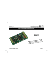
The central component of the BLIP device is a PIC16C765 manufactured by Microchip
Technology Inc. [1] The processor features a built in Universal Serial Bus (USB 1.1) along with
the standard simple behavior of the PIC Microchip microcontroller series. Through the USB,
BLIP can be interfaced with almost any modern computer. BLIP takes advantage of the Human
Interface Device (HID) class definitions for USB which allow it to be plugged into any USB port
and work without any need for previously installed drivers on Mac OS X or later and Windows
98 SE or later. The attached computer sees BLIP as a standard USB keyboard. This allows data
from BLIP to be acquired in any word processing or spread sheet software application, just as if
someone were typing the data on a standard USB keyboard.
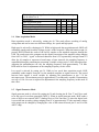
1.3 Functions
BLIP v. 1.1 has five primary functions: signal generator, frequency counter, period duration
timer, data acquisition, and event logger. The desired function is selected by configuring four
bits with the inputs on pins 37-40* (see Table 1). The bits can be changed at anytime. However,
the new settings will not take effect until BLIP is reset either cycling the power off and then on,
or by pressing the reset button connected to pin 1. BLIP must be plugged into a USB port in
order for any of the functions to work. Some of the modes have various functions within them
that rely on the jumper settings after the jumper that determines the mode, such as the signal
generator. These are explained in sections describing the individual modes.
Note that all pin number connections indicated in this user manual (except for those referring to
the jumper settings on pins 37-40 and when a specific chip is specified) will refer to the nine pin
receptacle on the BLIP PCB. See Table 4 in Section 2.1 of this manual for a reference of the
connections to the nine pin receptacle.
*
Bits are set to 1 (+5V) by removing the jumper and cleared to 0 (0V) by inserting the jumper.
3
Table 1: Jumper settings for mode selection ("-" indicates setting
can be either 0 or 1)
Pin Number
40
39
38
37
Data Acquisition Mode
1
Signal Generator Mode
0
1
Frequency Counter Mode
0
0
1
Event Logger Mode
0
0
0
1
Period Duration Timer
0
0
1
1
1.4 Data Acquisition Mode
Data acquisition mode is selected by setting pin 40. This mode allows recording of analog
voltage data and can be run at two different settings, low speed and high speed.
High speed is selected by clearing pin 39. While in high-speed data acquisition mode, BLIP will
continually sample and record the voltage on pin 6 of the receptacle. When the button on pin 6 is
pressed, BLIP offloads the result of the last 64 samples to the attached computer through the
USB. The results sent to the computer are the digital conversions of the sampled voltage ranging
from 0.00V to 5.00V, “typed” as decimal characters from 0-255 separated by carriage returns. To
allow the 64 samples to represent a broad range of time intervals, the sampling frequency is
controllable through a potentiometer presenting a variable voltage at pin 3 of the microprocessor.
Adjusting the potentiometer will vary the sampling frequency from approximately 7-50 kHz.
BLIP must be reset for adjustments to the sampling frequency to take effect.
Low speed is selected by setting pin 39. While in low speed data acquisition mode, BLIP
continually sends samples from pin 6 to the attached computer at regular intervals. The period
between each sample is made variable by adjusting the potentiometer at pin 3 of the
miccroprocessor. The maximum period is approximately 3 seconds and is capable of transmitting
at a rate of 6 Hz. No reset is required for adjustments to the sampling frequency in this mode to
take effect.
1.5 Signal Generator Mode
Signal generator mode is selected by setting pin 39 and clearing pin 40. Pins 37 and 38 are used
to set the type of waveform generated (Table 2). When in signal generator mode, BLIP sends a
series of bytes to an external AD557 (Analog Devices) D/A converter [2] where the digital code
is converted into an analog voltage ranging from 0V to approximately 4V (the maximum voltage
at the output can be changed by changing the value of the resistor between pin 15 and 16 of the
AD557 chip).
4
Table 2: Signal Generator waveform setting logic table.
Signal Type
Pin 38
Pin 37
Square Wave
0
0
Sine Wave
1
0
Triangle Wave
1
1
High-Speed Square Wave
0
1
The standard square wave, sine wave, and triangle wave, have a variable frequency between
approximately 460 Hz and 6.8 kHz. Adjusting the potentiometer varies that frequency. While in
one of these three modes, pressing the button connected to pin 6 sends the approximate
frequency (in Hz) of the signal being generated to the computer through the USB as four decimal
characters followed by a carriage return.
A fourth waveform setting, high-speed square-wave, provides a larger frequency range with a
much higher maximum frequency. In this setting, adjusting the potentiometer varies the
frequency between approximately 2 kHz and 80 kHz. Unlike in the other waveform settings,
BLIP is unable to report the frequency of the signal when in the high-speed square wave setting.
1.6 Frequency Counter Mode
Frequency Counter mode is selected by setting pin 38 and clearing pins 37, 39, and 40. While in
frequency counter mode, BLIP counts the number of rising edges seen on pin 8 of the receptacle
that occur in one second. In order for BLIP to see the signal on pin 8, the signal must be a square
wave oscillating between ground and +5V. Pressing the report button on pin 6 causes BLIP to
report the number of rising edges seen in the last second in a special decimal format representing
two bytes in a 16 bit binary number. The high byte (HB) is reported followed by a tab and then
the low byte (LB) is reported followed by a carriage return. The frequency (ω), between 0 and
65535, is then given by a simple algebraic equation (Equation 1).
" = 256( HB) + LB
(1)
The number rolls over at the decimal number 65536, and therefore, frequencies being measured
should be kept under 65 kHz to ensure accurate measurements.
!
1.7 Period Duration Timer Mode
Period Duration Counter mode is selected by setting pins 37-38 and clearing pins 39-40. The
duration timer can be used to measure the time between digital impulses on pin 9 of the
receptacle. For the duration timer to function, an external clock source must be provided on pin
8. The external clock source will continually increment a 16-bit timer register. The current state
of the 16-bit timer register is sent to the attached computer whenever a digital impulse occurs on
pin 9 (the state is captured on the rising edge and reported on the falling edge). The state of the
timer is reported in the same method as with the frequency counter, with a high byte and a low
5
byte. If the reported states are converted into decimal numbers, the measured duration then
becomes:
duration(t ) = x(t ) ! x(t ! 1)
Where x(t) is the acquired sample and x(t-1) is the previous sample. Since the 16-bit number will
role over to 0 after 65535, it is necessary to use a mod function to obtain continuously accurate
results. It also should be noted that the time between impulses cannot be more than 65535 times
the period of the clock input frequency. Currently the duration timer has only been tested with a
1.0 kHz clock input
1.8 Event Logger Mode
Event Logger mode is selected by setting pin 37 and clearing pins 38-40. The event logger
continuously monitors pins 33-36 for any change in digital state. A clock is needed on pin 4. On
each falling edge of pin 7, BLIP will transfer the current state of the monitored pins to the
attached computer in the form of 1’s and 0’s. BLIP reports the state of each pin starting with pin
2 of the receptacle and ending with pin 5 separated by tabs and followed by a carriage return.
Due to the time lag during which BLIP is transferring data to the computer, input frequencies
must be kept below 3 Hz for accurate monitoring.
2. Construction
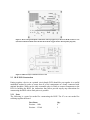
2.1 Pin-outs and Schematics
The following figures detail the Pin-outs of the actual BLIP processor, the schematics of the
BLIP system, and the printed layers of the PCB on which the BLIP is built.
Note the following about this particular implementation: The single 0.2 µF capacitor at pin 18 of
the microprocessor has been replaced by two 0.1 µF capacitors in parallel.
6
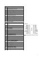
Table 3: PIC16C765 pin usages
Pin # Usage
1
Reset button/Power-on reset
2
Analog data input
3
Analog control input
4
Event Logger Clock Input
5
Unimplemented I/O pin
6
Report button
7
Unimplemented I/O pin
8
Unimplemented I/O pin
9
Unimplemented I/O pin
10
Unimplemented I/O pin
11
+5V
12
Ground
13
Crystal oscillator
14
Crystal oscillator
15
Duration Timer Clock/Frequency Counter
Input
17
Duration Timer Input
18
USB
19
D/A converter
20
D/A converter
21
D/A converter
22
D/A converter
23
USB
24
USB
25
Unimplemented I/O pin
26
Unimplemented I/O pin
27
D/A converter
28
D/A converter
29
D/A converter
30
D/A converter
31
Ground – internally connected
32
+5V – internally connected
33
Event Logger Input
34
Event Logger Input
35
Event Logger Input
36
Event Logger Input
37
Operating mode switches
38
Operating mode switches
39
Operating mode switches
40
Operating mode switches
Figure 1: Pin Diagram of PIC16C765 40-Pin
DIP [1]
7
Table 4: PCB/IC Pin-out Reference
BLIP PCB Pin-out
IC Pin-out
1
AD557 – 16
2
BLIP – 33
3
BLIP – 34
4
BLIP – 35
5
BLIP – 36
6
BLIP – 2
7
BLIP – 4
8
BLIP – 15
9
BLIP – 17
Usage
Signal Generator Output
Event Logger Input
Event Logger Input
Event Logger Input
Event Logger Input
Analog Data Input
Event Logger Clock Input
Duration Timer Clock/Frequency Counter Input
Duration Timer Input
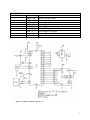
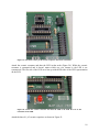
Figure 2: Complete schematic of BLIP v. 1.1
8
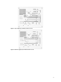
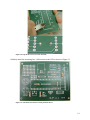
Figure 3: Top copper layer of PCB version 1.x rev2
Figure 4: Bottom copper layer of PCB version 1.x rev2
9
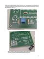
Figure 5: Power and ground plane connections with top copper layer shown for PCB version 1.x rev2
(note bad connection which causes the first bit in Event Logger mode to interrupt the program).
Figure 6: Silkscreen layer of PCB version 1.x rev2
2.2 BLIP PCB Construction
Putting together a device on a printed circuit board (PCB) should be put together in a careful
methodical method in order to ensure that all of the components are cleanly connected with
minimal headache. While not the only reasonable order in which to connect components to the
PCB for building the BLIP, the instructions that follow provide step-by-step instructions for
constructing the BLIP with as little pain as is possible.
2.2.1 Parts
The following is a parts list needed for constructing the BLIP. The ICs are not needed for
soldering together the board.
Part Name
Resistor – 1 kΩ
Resistor – 1.5 kΩ
Qty.
4
1
10
Single Turn Potentiometer – 100 kΩ
Ceramic Resonator – 6.00 MHz
Ceramic Disc Capacitor – 0.1 µF
Electrolytic Capacitor – 10 µF
LED – Red
PC Board Receptacle – 3 Position
PC Board Receptacle – 9 Position
IC Socket – 40 Pin DIP
IC Socket – 16 Pin DIP
IC Socket – 8 Pin DIP
Header Pins – 2 x 4
Header
Pushbutton Switch – NO
USB Receptical – B-type
1
1
3
2
1
1
1
1
1
1
1
4
2
1
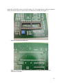
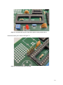
Figure 7: These are the parts listed above required to solder together the BLIP (PCB and
ICs not shown).
2.2.2 Printed Circuit Board
The PCB for the BLIP has a total of five printed layers. The front and back copper layers connect
the various pins of the components together. There are also two layers inside the PCB that act as
power and ground connections. Specific holes are connected to these planes to provide a ground
connection or +5V connection at those sites. The last printed layer is the white silkscreen layer
that has various annotations to label and outline where the various components go and their
orientation.
Over top of the front and back copper layers is a coating with a material called solder mask. This
insulates the traces and protects them from accidental contact with other conductors. The solder
pads around the holes are not coated with this material. Solder mask is usually green (as is the
case with the BLIP), but blue, red, and yellow are also sometimes used on PCBs.
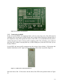
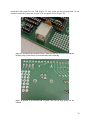
11
Figure 8: Front side of the BLIP PCB.
2.2.3 Constructing the BLIP
In the case of the BLIP, all component bodies will sit on the front side of the PCB and all
soldering will be on the back. So that all parts can be easily soldered into place with the body of
the component resting flush against the surface of the PCB, it is recommended that all parts be
soldered into place in order of lowest profile to highest profile. This will allow you to solder all
parts into place without worrying about any of them falling away from the PCB while you are
trying to solder it.
For the BLIP, the lowest profile components are the resistors. Start with the 1.5 kΩ resistor and
bend the leads down at a 90˚ angle as close to the body of the resistor as possible (Figure 9).
Figure 9: 1.5 kΩ resistor with leads bent down.
Insert the leads of the 1.5 kΩ resistor into the holes of the PCB in the position shown in Figure
10.
12
Figure 10: 1.5 kΩ resistor inserted into PCB.
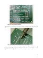
Turn the board over and resting it on the table, solder the two leads onto the solder pads (Figure
11).
Figure 11: Solder the two leads of the 1.5 kΩ resistor onto the solder pads.
After you have two good solder joints, clip the excess of the leads off to leave behind 1/16 to 1/8
inch above the PCB (Figure 12).
13
Figure 12: Clip off the excess wire from the leads.
Similarly attach the remaining four 1 kΩ resistors to the PCB as shown in Figure 13.
Figure 13: Attach the 1 kΩ resistors in the positions shown.
14
Attach the 100 kΩ potentiometer to the PCB (Figure 14). You might want to use something to
prop up the other side of the PCB while soldering so that the board lays flat against the bottom of
the potentiometer (Figure 15).
Figure 14: Attach the 100 kΩ potentiometer as shown.
Figure 15: Whenever possible, make sure that the component is flat against the PCB. You
may need to prop up one side of the PCB while soldering to allow for this.
15
Attach the 40 Pin DIP socket to the PCB (Figure 16). You might want to solder two opposite
corner pins first to secure it in place while you solder the rest of the pins (Figure 17).
Figure 16: Attach the 40 Pin DIP socket.
Figure 17: Soldering two opposite pins first helps hold a large component in place while you
solder the rest of the pins.
16
Attach the other two DIP sockets (Figure 18).
Figure 18: Attach the other two DIP sockets in the same manner as the 40 Pin DIP socket.
Attach the PC Board receptacles to their respective positions (Figure 19).
17
Figure 19: Attach the 3 and 9 pin PC board receptacles. Note their orientation.
Attach the ceramic resonator and then the LED in that order (Figure 20). While the ceramic
resonator is symmetrical and it doesn’t matter which way you connect it, the LED is not
symmetrical. The flat side of the LED must line up with the flat side of the LED representation
on the PCB.
Figure 20: Attach the ceramic resonator and then the LED to the PCB. Be ware of the
orientation of the LED.
Attach the three 0.1 µF ceramic capacitors as shown in Figure 21.
18
Figure 21: Attach the three 0.1 µF ceramic disk capacitors in the positions shown.
Attach the header pins as shown in Figure 22.
Figure 22: Attach the header pins to the PCB.
19
Attach the USB receptacle to the PCB (Figure 23). Only solder the four grouped leads. Do not
attempt to solder the prongs that are part of the receptacle chassis (Figure 24).
Figure 23: Attach the USB receptacle as shown. Make sure that it is flat against the PCB and
the large prongs on the side are secure in their holes before soldering.
Figure 24: Bottom of the attached USB receptacle. Note that the large prongs are not
soldered.
20
Attach the two 10 µF electrolytic capacitors (Figure 25). Make sure that the longer lead of the
capacitors go into the holes marked with a “+” symbol.
Figure 25: Attach the 10 µF capacitors to the PCB. Make sure you have their orientation
correct.
Attach the two pushbuttons (Figure 26). Be sure that the flat of the button is lined up with the flat
part of the button representation on the PCB.
Figure 26: Attach the two pushbuttons to the PCB. Make sure to have their orientation
correct.
21
Plug the headers into the header pins as shown in Figure 27.
Figure 27: Plug the headers into the header pins. Make sure they are oriented the same as in
the picture.
At this point the construction of the board is complete. The final step is to insert the ICs into their
sockets. The ICs pins will not fit perfectly into the sockets without some bending. A reliable way
to do this is to first rest one row of pins into their position in the socket without pushing them in.
Then push the chip towards those pins until the other row of pins will fit into their positions on
the socket. Make sure to note the orientation of the chips. The notch on the chip should line up
with the notch in the socket, which should also line up with the notch in the graphical socket
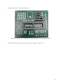
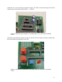
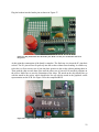
representation on the PCB. See Figure 28 for the completed BLIP.
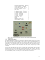
Figure 28: Completed BLIP with all components.
22
3. References
1. PIC16C745/765: 8-Bit CMOS Microcontrollers with USB. Microchip Technology Inc.,
2000.
2. AD557: Low Cost, Complete µP-Compatible 8-Bit DAC. Analog Devices, Inc., 2001.
23