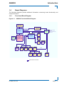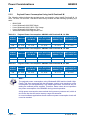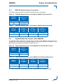
1
AM4002
Processor AMC Module based on
the Intel® Pentium® M Processor with
Doc. ID: 33204, Rev. 02
December 12, 2008
User Guide
PRELIMINARY
the Intel® E7320 Chipset
Preface
AM4002
Revision History
Publication Title:
AM4002: Processor AMC Module based on the Intel® Pentium® M
Processor with the Intel® E7320 Chipset
Doc. ID: 33204
PRELIMINARY
Rev.
Brief Description of Changes
Date of Issue
01
Initial issue
Jun 23, 2006
02
General update, Appendix A “AMIBIOS8” removed
Dec 12, 2008
Imprint
Kontron Modular Computers GmbH may be contacted via the following:
MAILING ADDRESS
TELEPHONE AND E-MAIL
Kontron Modular Computers GmbH
Sudetenstraße 7
D - 87600 Kaufbeuren Germany
+49 (0) 800-SALESKONTRON
[email protected]
For further information about other Kontron products, please visit our Internet web site:
www.kontron.com
Disclaimer
Copyright © 2008 Kontron AG. All rights reserved. All data is for information purposes only and
not guaranteed for legal purposes. Information has been carefully checked and is believed to
be accurate; however, no responsibility is assumed for inaccuracies. Kontron and the Kontron
logo and all other trademarks or registered trademarks are the property of their respective owners and are recognized. Specifications are subject to change without notice.
Page ii
ID 33204, Rev. 02
AM4002
Preface
Revision History .........................................................................................................ii
Imprint ........................................................................................................................ii
Disclaimer ..................................................................................................................ii
Table of Contents ...................................................................................................... iii
List of Tables ............................................................................................................ vii
List of Figures ...........................................................................................................ix
Proprietary Note ........................................................................................................xi
Trademarks ...............................................................................................................xi
Environmental Protection Statement .........................................................................xi
Explanation of Symbols ........................................................................................... xii
For Your Safety ....................................................................................................... xiii
High Voltage Safety Instructions ......................................................................... xiii
Special Handling and Unpacking Instructions .................................................... xiii
General Instructions on Usage ........................................................................... xiv
Two Year Warranty ...................................................................................................xv
1.
Introduction ............................................................................. 1 - 3
1.1 AdvancedTCA System Overview ............................................................ 1 - 3
1.2 Board Overview ....................................................................................... 1 - 4
1.2.1
Board Introduction .......................................................................... 1 - 4
1.2.2
Board-Specific Information ............................................................. 1 - 5
1.3 System Relevant Information .................................................................. 1 - 6
1.4 Board Diagrams ...................................................................................... 1 - 7
1.4.1
Functional Block Diagram ............................................................... 1 - 7
1.4.2
Front Panel ..................................................................................... 1 - 8
1.4.3
Board Layouts ................................................................................ 1 - 9
1.5 Technical Specification .......................................................................... 1 - 10
1.6 Kontron Software Support ..................................................................... 1 - 14
1.7 Applied Standards ................................................................................. 1 - 15
1.8 Related Publications ............................................................................. 1 - 16
2.1 CPU, Memory and Chipset ...................................................................... 2 - 3
2.1.1
CPU ................................................................................................ 2 - 3
2.1.2
Memory ........................................................................................... 2 - 4
2.1.3
Intel® E7320 Chipset Overview ...................................................... 2 - 5
ID 33204, Rev. 02
Page iii
PRELIMINARY
Table of Contents
Preface
AM4002
2.1.4
Memory Controller Hub E7320 ........................................................2 - 5
2.1.5
I/O Controller Hub 6300ESB ...........................................................2 - 5
PRELIMINARY
2.2 Peripherals ...............................................................................................2 - 6
2.2.1
Timer ...............................................................................................2 - 6
2.2.2
Watchdog Timer ..............................................................................2 - 6
2.2.3
Battery .............................................................................................2 - 6
2.2.4
Power Monitor and Reset Generation .............................................2 - 6
2.2.5
SMBus Devices ...............................................................................2 - 7
2.2.6
Serial EEPROM ..............................................................................2 - 7
2.2.7
FLASH Memory ...............................................................................2 - 7
2.2.7.1
BIOS FLASH (Firmware Hub) .................................................2 - 7
2.2.7.2
CompactFlash Controller ........................................................2 - 7
2.3 Board Interfaces ......................................................................................2 - 8
2.3.1
Front Panel LEDs ............................................................................2 - 8
2.3.2
General Purpose DIP Switch ........................................................2 - 10
2.3.3
Debug Interface .............................................................................2 - 10
2.3.4
USB Host Interface ....................................................................... 2 - 11
2.3.5
COM Port ......................................................................................2 - 12
2.3.6
Gigabit Ethernet ............................................................................2 - 13
2.4 AMC Interconnection .............................................................................2 - 14
2.4.1
Fabric Interface .............................................................................2 - 14
2.4.2
Synchronization Clock Interface ....................................................2 - 15
2.4.3
System Management Interface .....................................................2 - 16
2.4.4
JTAG Interface ..............................................................................2 - 16
2.4.5
Module Power Interface ................................................................2 - 16
2.4.6
Pinout of AMC Edge Connector J1 ...............................................2 - 16
2.5 Module Management .............................................................................2 - 20
2.5.1
Module Management Controller ....................................................2 - 20
2.5.1.1
MMC Signals Implemented on the AM4002 .........................2 - 21
3.1 Safety Requirements ...............................................................................3 - 3
3.2 AM4002 Hot Swap Insertion Procedures .................................................3 - 4
3.3 AM4002 Hot Swap Extraction Procedures ..............................................3 - 5
3.4 Installation of AM4002 Peripheral Devices ..............................................3 - 6
3.4.1
Page iv
Installation of USB Host Devices ....................................................3 - 6
ID 33204, Rev. 02
AM4002
Preface
3.5 Software Installation ................................................................................ 3 - 6
4.1 DIP Switch Configuration ........................................................................ 4 - 3
4.1.1
Module LED Configuration (POST Code) ....................................... 4 - 4
4.1.2
BIOS Firmware Hub Flash Configuration ....................................... 4 - 4
4.1.3
Boot Order Configuration ................................................................ 4 - 4
4.1.4
Clear BIOS CMOS Configuration ................................................... 4 - 4
4.2 Interrupts ................................................................................................. 4 - 5
4.3.1
Memory Map for the 1st Megabyte ................................................. 4 - 6
4.3.2
I/O Address Map ............................................................................. 4 - 7
4.4 AM4002-Specific Registers ..................................................................... 4 - 9
4.4.1
BIOS Boot Order Control Register .................................................. 4 - 9
4.4.2
Watchdog Timer Control Register ................................................ 4 - 10
4.4.3
AMC Geographic Addressing Register ......................................... 4 - 12
4.4.4
Hardware and Logic Revision Index Register ............................... 4 - 12
4.4.5
Reset Status Register ................................................................... 4 - 13
4.4.6
I/O Status Register ........................................................................ 4 - 14
4.4.7
I/O Configuration Register ............................................................ 4 - 15
4.4.8
Board ID Register ......................................................................... 4 - 16
4.4.9
Board Interrupt Configuration Register ......................................... 4 - 17
4.4.10 Hot Swap Status Register ............................................................. 4 - 17
4.4.11 Module LED Configuration Register 0 .......................................... 4 - 18
4.4.12 AMC LED Configuration Register 1 .............................................. 4 - 19
4.4.13 Module LED Control Register 0 .................................................... 4 - 20
4.4.14 AMC LED Control Register 1 ........................................................ 4 - 21
4.4.15 Delay Timer Control/Status Register ............................................ 4 - 22
4.5 MMC-Specific Registers ........................................................................ 4 - 23
4.5.1
MMC Configuration Register 0 ..................................................... 4 - 23
4.5.2
MMC Interrupt Configuration Register .......................................... 4 - 24
4.5.3
IPMI Keyboard Control Style Interface ......................................... 4 - 25
5.1 AM4002 Voltage Ranges ........................................................................ 5 - 3
5.2 Carrier Power Requirements ................................................................... 5 - 4
5.2.1
Payload Power ................................................................................ 5 - 4
5.2.2
Payload and MMC Voltage Ramp ................................................... 5 - 4
ID 33204, Rev. 02
Page v
PRELIMINARY
4.3 Memory Map ........................................................................................... 4 - 6
Preface
5.2.3
AM4002
Module Management Power Consumption .....................................5 - 4
5.3 Payload Power Consumption of the AM4002 ..........................................5 - 5
5.3.1
Payload Power Consumption Using Intel® Celeron® M .................5 - 5
5.3.2
Payload Power Consumption Using Intel® Pentium® M ................5 - 6
5.3.3
IPMI FRU Payload Power Consumption .........................................5 - 7
Payload Start-Up Current of the AM4002 ...............................................5 - 7
PRELIMINARY
5.4
Page vi
ID 33204, Rev. 02
AM4002
Preface
1-1
System Relevant Information ................................................................... 1 - 6
1-2
AM4002 Main Specifications .................................................................. 1 - 10
1-3
Applied Standards .................................................................................. 1 - 15
1-4
Related Publications .............................................................................. 1 - 16
2-1
Intel® Celeron® M Processor Supported on the AM4002 ....................... 2 - 3
2-2
Processor Maximum Power Dissipation (Intel® Celeron® M) ................. 2 - 3
2-3
Intel® Pentium® M Processors Supported on the AM4002 ..................... 2 - 4
2-4
Processor Maximum Power Dissipation (Intel® Pentium® M) ................. 2 - 4
2-5
SMBus Device Addresses ....................................................................... 2 - 7
2-6
EEPROM Address Map ........................................................................... 2 - 7
2-7
AMC LEDs Function ................................................................................ 2 - 8
2-9
POST Code Example ............................................................................... 2 - 9
2-10
MMC Control LEDs Description ............................................................... 2 - 9
2-8
Module LEDs Function ............................................................................. 2 - 9
2-11
DIP Switch Functions ............................................................................. 2 - 10
2-12
Mini USB Type A Connector J3 ............................................................. 2 - 11
2-13
Serial Port Con. J2 (COM1) Pinout ........................................................ 2 - 12
2-14
Reserved Pins on the AMC Edge Connector J1 .................................... 2 - 16
2-15
Pinout of AMC Edge Connector J1 ........................................................ 2 - 17
2-16
Processor and Chipset Supervision ....................................................... 2 - 21
2-17
AMC Signals .......................................................................................... 2 - 21
2-18
Onboard Power Supply Supervision ...................................................... 2 - 21
2-19
Temperature Signals .............................................................................. 2 - 22
4-1
DIP Switch Functions ............................................................................... 4 - 3
4-2
Module LED Configuration (POST Code) ................................................ 4 - 4
4-3
BIOS Firmware Hub Flash Configuration ................................................. 4 - 4
4-4
BIOS Boot Order Configuration ............................................................... 4 - 4
4-5
BIOS CMOS Configuration ...................................................................... 4 - 4
4-6
Interrupt Setting ....................................................................................... 4 - 5
4-7
Memory Map for the 1st Megabyte .......................................................... 4 - 6
4-8
I/O Address Map ...................................................................................... 4 - 7
4-9
BIOS Boot Order Control Register ........................................................... 4 - 9
ID 33204, Rev. 02
Page vii
PRELIMINARY
List of Tables
PRELIMINARY
Preface
AM4002
4-10
Watchdog Timer Control Register .......................................................... 4 - 11
4-11
Geographic Addressing Register ........................................................... 4 - 12
4-12
Hardware and Logic Index Revision Index Register .............................. 4 - 12
4-13
Reset Status Register ............................................................................. 4 - 13
4-14
I/O Status Register ................................................................................. 4 - 14
4-15
I/O Configuration Register ...................................................................... 4 - 15
4-16
Board ID Register ................................................................................... 4 - 16
4-17
Board Interrupt Configuration Register ................................................... 4 - 17
4-18
Hot Swap Status Register ...................................................................... 4 - 17
4-19
Module LED Configuration Register 0 .................................................... 4 - 18
4-20
AMC LED Configuration Register 1 ........................................................ 4 - 19
4-21
Module LED Control Register 0 .............................................................. 4 - 20
4-22
AMC LED Control Register 1 ................................................................. 4 - 21
4-23
Delay Timer Control/Status Register ..................................................... 4 - 22
4-24
MMC Configuration Register 0 ............................................................... 4 - 23
4-25
Firmware Update Functions ................................................................... 4 - 24
4-26
MMC Interrupt Configuration Register .................................................... 4 - 24
5-1
DC Operational Input Voltage Ranges ..................................................... 5 - 3
5-2
Payload Power Consumption: AM4002 with Celeron® M, 1.0 GHz ......... 5 - 5
5-3
Payload Power Consumption: AM4002 with Pentium® M, 1.4 GHz ........ 5 - 6
5-4
Payload Power Consumption: AM4002 with Pentium® M, 1.8 GHz ........ 5 - 6
5-5
Payload Power Consumption: AM4002 with Pentium® M, 2.0 GHz ........ 5 - 6
5-6
IPMI FRU Payload Power Consumption: AM4002 with Celeron® M ....... 5 - 7
5-7
IPMI FRU Payload Power Consumption: AM4002 with Pentium® M ....... 5 - 7
5-8
Payload Start-Up Current of the AM4002 with Celeron® M Processor .... 5 - 7
5-9
Payload Start-Up Current of the AM4002 with Pentium® M Processor ... 5 - 7
Page viii
ID 33204, Rev. 02
AM4002
Preface
1-1
AM4002 Functional Block Diagram .......................................................... 1 - 7
1-2
AM4002 Full-Height Front Panel and Lexan Label .................................. 1 - 8
1-3
AM4002 Board Layout (Top View) ........................................................... 1 - 9
1-4
AM4002 Board Layout (Bottom View) ...................................................... 1 - 9
2-1
Front Panel LEDs ..................................................................................... 2 - 8
2-2
Mini USB Type A Connector J3 ............................................................. 2 - 11
2-3
Adapter for Mini USB Type A Connector to USB Type A Connector ..... 2 - 11
2-4
Serial Port Connector J2 (COM1) .......................................................... 2 - 12
2-5
AM4002 Port Mapping ........................................................................... 2 - 15
2-6
AM4002 Temperature Sensor Placement .............................................. 2 - 22
2-7
Memory Module Temperature Sensor .................................................... 2 - 22
3-1
Adapter for Mini USB Type A Connector to USB Type A Connector ....... 3 - 6
4-1
DIP Switch ............................................................................................... 4 - 3
ID 33204, Rev. 02
Page ix
PRELIMINARY
List of Figures
PRELIMINARY
Preface
AM4002
This page has been intentionally left blank.
Page x
ID 33204, Rev. 02
AM4002
Preface
Proprietary Note
This document contains information proprietary to Kontron. It may not be copied or transmitted by any means, disclosed to others, or stored in any retrieval system or media without the
prior written consent of Kontron or one of its authorized agents.
The information contained in this document is, to the best of our knowledge, entirely correct.
However, Kontron cannot accept liability for any inaccuracies or the consequences thereof, or
for any liability arising from the use or application of any circuit, product, or example shown in
this document.
Trademarks
This document may include names, company logos and trademarks, which are registered
trademarks and, therefore, proprietary to their respective owners.
Environmental Protection Statement
This product has been manufactured to satisfy environmental protection requirements where
possible. Many of the components used (structural parts, printed circuit boards, connectors,
batteries, etc.) are capable of being recycled.
Final disposition of this product after its service life must be accomplished in accordance with
applicable country, state, or local laws or regulations.
ID 33204, Rev. 02
Page xi
PRELIMINARY
Kontron reserves the right to change, modify, or improve this document or the product
described herein, as seen fit by Kontron without further notice.
Preface
AM4002
Explanation of Symbols
Caution, Electric Shock!
This symbol and title warn of hazards due to electrical shocks (> 60V)
when touching products or parts of them. Failure to observe the precautions indicated and/or prescribed by the law may endanger your
life/health and/or result in damage to your material.
Please refer also to the section “High Voltage Safety Instructions” on
the following page.
Warning, ESD Sensitive Device!
PRELIMINARY
This symbol and title inform that electronic boards and their components are sensitive to static electricity. Therefore, care must be taken
during all handling operations and inspections of this product, in
order to ensure product integrity at all times.
Please read also the section “Special Handling and Unpacking
Instructions” on the following page.
Warning!
This symbol and title emphasize points which, if not fully understood
and taken into consideration by the reader, may endanger your health
and/or result in damage to your material.
Note ...
This symbol and title emphasize aspects the reader should read
through carefully for his or her own advantage.
Page xii
ID 33204, Rev. 02
AM4002
Preface
For Your Safety
Your new Kontron product was developed and tested carefully to provide all features necessary to ensure its compliance with electrical safety requirements. It was also designed for a
long fault-free life. However, the life expectancy of your product can be drastically reduced by
improper treatment during unpacking and installation. Therefore, in the interest of your own
safety and of the correct operation of your new Kontron product, you are requested to conform
with the following guidelines.
High Voltage Safety Instructions
All operations on this device must be carried out by sufficiently skilled
personnel only.
Caution, Electric Shock!
Before installing any piggybacks or carrying out maintenance operations always ensure that your mains power is switched off.
Serious electrical shock hazards can exist during all installation,
repair and maintenance operations with this product. Therefore,
always unplug the power cable and any other cables which provide
external voltages before performing work.
Special Handling and Unpacking Instructions
ESD Sensitive Device!
Electronic boards and their components are sensitive to static electricity. Therefore, care must be taken during all handling operations
and inspections of this product, in order to ensure product integrity at
all times.
Warning!
This product has gold conductive fingers which are susceptible to contamination. Take care not to touch the gold conductive fingers of the
AMC edge connector when handling the board.
Failure to comply with the instruction above may cause damage to the
board or result in improper system operation.
Do not handle this product out of its protective enclosure while it is not used for operational purposes unless it is otherwise protected.
Whenever possible, unpack or pack this product only at EOS/ESD safe work stations. Where
a safe work station is not guaranteed, it is important for the user to be electrically discharged
before touching the product with his/her hands or tools. This is most easily done by touching a
metal part of your system housing.
ID 33204, Rev. 02
Page xiii
PRELIMINARY
Warning!
Preface
AM4002
It is particularly important to observe standard anti-static precautions when changing piggybacks, ROM devices, jumper settings etc. If the product contains batteries for RTC or memory
backup, ensure that the board is not placed on conductive surfaces, including anti-static plastics or sponges. They can cause short circuits and damage the batteries or conductive circuits
on the board.
General Instructions on Usage
PRELIMINARY
In order to maintain Kontron’s product warranty, this product must not be altered or modified in
any way. Changes or modifications to the device, which are not explicitly approved by Kontron
and described in this manual or received from Kontron’s Technical Support as a special handling instruction, will void your warranty.
This device should only be installed in or connected to systems that fulfill all necessary technical and specific environmental requirements. This applies also to the operational temperature
range of the specific board version, which must not be exceeded. If batteries are present, their
temperature restrictions must be taken into account.
In performing all necessary installation and application operations, please follow only the instructions supplied by the present manual.
Keep all the original packaging material for future storage or warranty shipments. If it is necessary to store or ship the board, please re-pack it as nearly as possible in the manner in which
it was delivered.
Special care is necessary when handling or unpacking the product. Please consult the special
handling and unpacking instruction on the previous page of this manual.
Page xiv
ID 33204, Rev. 02
AM4002
Preface
Two Year Warranty
Kontron warrants their own products, excluding software, to be free from manufacturing and
material defects for a period of 24 consecutive months from the date of purchase. This warranty is not transferable nor extendible to cover any other users or long-term storage of the
product. It does not cover products which have been modified, altered or repaired by any
other party than Kontron or their authorized agents. Furthermore, any product which has
been, or is suspected of being damaged as a result of negligence, improper use, incorrect
handling, servicing or maintenance, or which has been damaged as a result of excessive current/voltage or temperature, or which has had its serial number(s), any other markings or
parts thereof altered, defaced or removed will also be excluded from this warranty.
If the customer’s eligibility for warranty has not been voided, in the event of any claim, he may
return the product at the earliest possible convenience to the original place of purchase,
together with a copy of the original document of purchase, a full description of the application
the product is used on and a description of the defect. Pack the product in such a way as to
ensure safe transportation (see our safety instructions).
Kontron provides for repair or replacement of any part, assembly or sub-assembly at their own
discretion, or to refund the original cost of purchase, if appropriate. In the event of repair,
refunding or replacement of any part, the ownership of the removed or replaced parts reverts
to Kontron, and the remaining part of the original guarantee, or any new guarantee to cover
the repaired or replaced items, will be transferred to cover the new or repaired items. Any
extensions to the original guarantee are considered gestures of goodwill, and will be defined
in the “Repair Report” issued by Kontron with the repaired or replaced item.
Kontron will not accept liability for any further claims resulting directly or indirectly from any
warranty claim, other than the above specified repair, replacement or refunding. In particular,
all claims for damage to any system or process in which the product was employed, or any
loss incurred as a result of the product not functioning at any given time, are excluded. The
extent of Kontron liability to the customer shall not exceed the original purchase price of the
item for which the claim exists.
Kontron issues no warranty or representation, either explicit or implicit, with respect to its
products’ reliability, fitness, quality, marketability or ability to fulfil any particular application or
purpose. As a result, the products are sold “as is,” and the responsibility to ensure their suitability for any given task remains that of the purchaser. In no event will Kontron be liable for
direct, indirect or consequential damages resulting from the use of our hardware or software
products, or documentation, even if Kontron were advised of the possibility of such claims
prior to the purchase of the product or during any period since the date of its purchase.
Please remember that no Kontron employee, dealer or agent is authorized to make any modification or addition to the above specified terms, either verbally or in any other form, written or
electronically transmitted, without the company’s consent.
ID 33204, Rev. 02
Page xv
PRELIMINARY
Kontron grants the original purchaser of Kontron’s products a TWO YEAR LIMITED HARDWARE
WARRANTY as described in the following. However, no other warranties that may be granted or
implied by anyone on behalf of Kontron are valid unless the consumer has the express written
consent of Kontron.
PRELIMINARY
Preface
AM4002
This page has been intentionally left blank.
Page xvi
ID 33204, Rev. 02
Introduction
Chapter
1
Introduction
ID 33204, Rev. 02
Page 1 - 1
PRELIMINARY
AM4002
PRELIMINARY
Introduction
AM4002
This page has been intentionally left blank.
Page 1 - 2
ID 33204, Rev. 02
AM4002
1.
Introduction
1.1
AdvancedTCA System Overview
Introduction
The Kontron AMC cards can be integrated not only on Kontron ATCA carrier boards, but also
on a variety of AMC-supporting ATCA and proprietary carrier boards providing them with superior processing power and maximum design options. To learn more about the outstanding
features and advantages of Kontron ATCA carrier boards, please contact Kontron or visit the
Kontron web site.
ID 33204, Rev. 02
Page 1 - 3
PRELIMINARY
The Advanced Mezzanine Card (AMC) described in this manual operates with the Advanced
Telecom Computing Architecture (AdvancedTCA® or ATCA) defined by the PCI Industrial
Computer Manufacturers Group (PICMG). The main advantages of AdvancedTCA include high
throughput, multi-protocol support, high-power capability, hot swappability, high scalability, and
integrated system management. For further information regarding the AdvancedTCA
standards and their use, please consult the complete AdvancedTCA specification or visit the
PICMG web site.
Introduction
1.2
Board Overview
1.2.1
Board Introduction
AM4002
The AM4002 is a highly integrated CPU board implemented as a single-width, full-height
processor Advanced Mezzanine Card (AMC) module. The design is based on the low-power,
high-performance Intel® Celeron® M and Pentium® M processors combined with the highperformance E7320 chipset and the 6300ESB I/O controller hub.
PRELIMINARY
The board supports Intel® Celeron® M and Pentium® M processor versions in 90 nm technology and 479 µFCBGA package with frequencies ranging from 1.0 GHz up to 2.0 GHz providing
front side bus speeds of 400 MHz and 533 MHz. The processor is soldered on the AM4002 and
cannot be exchanged.
The board includes a dedicated memory module for up to 4 GB registered Double Data Rate
(DDR2) memory with Error Checking and Correcting (ECC) running at 400 MHz. A dual Gigabit
Ethernet controller utilizing a x4 lane PCI Express interconnection to the E7320 chipset ensures maximum data throughput between processor and memory. The AM4002 further provides up to 2 GB Flash memory via an onboard CompactFlash controller.
The AM4002 has full hot swap capability, which enables the board to be replaced, monitored
and controlled without having to shut down the ATCA carrier board or the system. A dedicated
Module Management Controller (MMC) is used to manage the board and support a defined
subset of Intelligent Platform Management Interface (IPMI) commands and PICMG (ATCA/
AMC) command extensions, which enables operators to detect and eliminate faults faster at
module level. This includes monitoring several onboard temperature conditions, board voltages
and the power supply status, managing hot swap operations, rebooting the board, etc. All in all,
IPMI enhances the board’s availability and reliability while reducing the operating costs and the
mean-time-to-repair.
As a “headless” AMC design (no onboard graphics controller), the AM4002 supports one USB
2.0 host interface to the front, one standard D-Sub RS-232 COM port, and a variety of highspeed interconnect topologies to the system, such as Dual Gigabit SerDes connection and
Dual Serial ATA storage interface in the common options region of the AMC port mapping, and
x4 PCI Express in the fat pipes of the AMC port mapping.
Optimized for high-performance, packet-based telecom systems, the AM4002 is targeted towards, but not limited to the telecom market application such as radio network controllers, storage control, routing and switching. The AM4002 also fits into all applications situated in
industrial environments, including I/O intensive applications. The careful design and selection
of high temperature resistant components ensure a high product availability. This, together with
a high level of scalability, reliability, and stability, make this state-of-the-art product a perfect
core technology for long-life embedded applications.
The board is offered with the generic Linux Board Support Package which supports various
Linux distributions including the Carrier Grade Linux (CGL) operating system. Please contact
Kontron for further information concerning other operating systems.
Page 1 - 4
ID 33204, Rev. 02
AM4002
1.2.2
Introduction
Board-Specific Information
Due to the outstanding features of the AM4002, such as superior processing power and flexible
interconnect topologies, this AMC board provides a highly scalable solution not only for a wide
range of telecom and data network applications, but also for several highly integrated industrial
environment applications with solid mechanical interfacing.
• Intel® Celeron® M and Pentium® M microprocessors up to 2.0 GHz in a 479 µFCBGA
package
• Up to 2048 kB L2 cache on-die, running at CPU speed
• 400 MHz and 533 MHz processor system bus
• E7320 chipset with the 6300ESB I/O controller hub
• Dedicated memory module for up to 4 GB DDR2 SDRAM memory running at 400 MHz
(PC3200)
• AMC interconnection
• Dual Gigabit SerDes connection in the common options region of the AMC port mapping
• Dual SATA storage interface in the common options region of AMC port mapping
• x4 PCI Express in the fat pipes region of the AMC port mapping (operates only as a
root complex controller)
• Full hot swap support
• Dual Gigabit Ethernet controller (82571EB-style)
• CompactFlash controller for up to 2 GB NAND Flash memory
• One front Mini USB 2.0 host port
• One standard D-Sub RS-232 COM port
• Console redirection via D-Sub RS-232 COM port
• Two redundant onboard FWH Flash chips for BIOS (2x1MB)
• Dedicated IPMI Module Management Controller with redundant Firmware Flash (2x128kB)
• Thermal management
• Watchdog Timer
• JTAG interface for debugging and manufacturing
• Standard temperature range: -5°C to + 55°C
• Passive heat sink solution
• Single-width, full-height and extended full-height AMC module
• Designed to be compliant with the following specifications:
• PICMG AMC.0, Advanced Mezzanine Card Specification R1.0
• PICMG AMC.1, PCI Express and Advanced Switching R1.0
• PICMG AMC.2, Gigabit Ethernet R1.0 (draft version)
• PICMG AMC.3, Storage Interfaces R1.0
• AMI BIOS
ID 33204, Rev. 02
Page 1 - 5
PRELIMINARY
Some of the AM4002's outstanding features are:
Introduction
1.3
AM4002
System Relevant Information
The following system relevant information is general in nature but should still be considered
when developing applications using the AM4002.
Table 1-1:
System Relevant Information
PRELIMINARY
SUBJECT
INFORMATION
Hardware Requirements
The AM4002 can be installed on any AMC-supporting carrier board with the following AMC connector port mapping:
• Common options region port 0-1
• Two Gigabit Ethernet SerDes (1000BASE-BX) ports
• Common options region port 2-3
• Two Serial ATA 150 ports
• Fat pipes region port 4-7
• One x4 PCI Express interface
For further information on the AMC interconnection, refer to section 2.4, “AMC
Interconnection”.
PCI Express Configuration
The AM4002 only supports the PCI Express root complex configuration; the nontransparent bridge functionality is not supported.
Operating Systems
The AM4002 is offered with the generic Linux Board Support Package which supports various Linux distributions including the Carrier Grade Linux (CGL) operating
system. Please contact Kontron for further information concerning other operating
systems.
Page 1 - 6
ID 33204, Rev. 02
AM4002
1.4
Introduction
Board Diagrams
The following diagrams provide additional information concerning board functionality and
component layout.
1.4.1
Functional Block Diagram
Figure 1-1:
AM4002 Functional Block Diagram
DDR2 PC400
up to 4 GB
E7320
x4 PCI Express
HUB 266 MB/s
PATA
USB 2.0
JTAG
CON
Intel®
Celeron® M
and
Pentium® M
LPC
AMC
CON
2x SATA
CF
Contr.
6300ESB
Flash
up to
2 GB
RS232
COM1 converter
Mini
USB 2.0
CON
BIOS
FWH
1 MB
AMC Interconnect
- 2xGbE
- 1x PCI Express (x4)
- 2x SATA
BIOS
FWH
1 MB
FPGA
MMC
Flash
128kB
Flash
128kB
D-Sub
CON
(COM1)
IPMB-L
Temp.
Power &
Hot
Swap
Front Panel Connectors
ID 33204, Rev. 02
Page 1 - 7
PRELIMINARY
Dual GbE
82571EB
x4 PCI Express
Introduction
1.4.2
AM4002
Front Panel
Figure 1-2:
AM4002 Full-Height Front Panel and Lexan Label
LEGEND:
AMC LEDs
PRELIMINARY
• HS (blue):
The hot swap indicator provides
basic feedback to the user on the
hot swap state of the module. The
HS LED states are off, short blink,
long blink, and on.
• LED1 (red):
MMC control and debug LED
• WD/LED2 (green): Watchdog or General Purpose;
when lit during boot-up, it
indicates a PCI reset is active
• TH/LED3 (amber): Overtemperature Status or
General Purpose; when lit during
boot-up, it indicates a power
failure
Module LEDs
AM4002
• MLED3 (green):
• MLED2 (green):
• MLED1 (green):
• MLED0 (green):
Ethernet port 0 link signal status or
General Purpose / BIOS POST
code LED.
Ethernet port 1 link signal status or
General Purpose / BIOS POST
code LED.
SATA and CompactFlash activity
status or General Purpose / BIOS
POST code LED.
MMC Debug or General Purpose /
BIOS POST code LED.
For further information on the LEDs used on the AM4002,
refer to section 2.3.1, “Front Panel LEDs”.
Page 1 - 8
ID 33204, Rev. 02
AM4002
1.4.3
Introduction
Board Layouts
Figure 1-3:
AM4002 Board Layout (Top View)
1
J2
J3
E7320
MCH
6300ESB
ICH
Module
LEDs
J1
J7
1
85
AMC LEDs
Figure 1-4:
AM4002 Board Layout (Bottom View)
170
DIP Switch
J9
(optional)
J1
86
ID 33204, Rev. 02
Page 1 - 9
PRELIMINARY
CPU
Introduction
1.5
Technical Specification
Table 1-2:
AM4002 Main Specifications
Processor and Memory
AM4002
PRELIMINARY
AM4002
SPECIFICATIONS
CPU
The AM4002 supports the following microprocessors:
• Intel® Celeron® M processors (90 nm) with 400 MHz PSB (Processor
Side Bus) in 479 µFCPGA packaging
• Intel® Celeron® M 1.0 GHz with 512 kB L2 cache (ultra low voltage)
• Intel® Pentium® M processors (90 nm) with 400 MHz and 533 MHz PSB
(Processor Side Bus) and SpeedStep® technology in 479 µFCBGA
packaging
• Intel® Pentium® M 1.4 GHz, 400 MHz FSB, 2 MB L2 cache, µFCBGA
(low voltage)
• Intel® Pentium® M 1.8 GHz, 400 MHz FSB, 2 MB L2 cache, µFCBGA
• Intel® Pentium® M 2.0 GHz, 533 MHz FSB, 2 MB L2 cache, µFCBGA
Please contact Kontron for further information concerning the suitability of
other Intel processors for use with the AM4002.
Memory
Main Memory:
• Up to 4 GB registered DDR2 (PC3200) SDRAM memory with ECC on
dedicated memory module
Cache structure:
• 64 kB L1 on-die full speed processor cache
• 32 kB for instruction cache
• 32 kB for data cache
• Up to 2048 kB L2 on-die full speed processor cache
FLASH Memory:
• Two redundant Firmware Hub (FWH) Flash chips (2x1MB) controlled by
the MMC
Mass Storage Device:
• Up to 2 GB NAND Flash via an onboard CompactFlash controller (true
IDE mode)
Serial EEPROM with 64 kbit
Page 1 - 10
ID 33204, Rev. 02
AM4002
AM4002 Main Specifications (Continued)
AM4002
Intel® E7320
Intel® E7320 Memory Controller Hub:
• Support for a single Intel® Celeron® M or Pentium® M microprocessor
• 64-bit AGTL/AGTL+ based System Bus interface at 400 MHz and
533 MHz
• System Memory interface with optimized support for DDR2 SDRAM
memory at 400 MHz with ECC
• Two x4 PCI Express ports
• RASUM (Reliability, Availability, Serviceability, Usability, and Manageability) features:
• Memory error detection and reporting of 1- and 2-bit errors including
correction of 1-bit failures
• Integrated Memory Scrub Engine, which logs any uncorrectable
memory errors
• Support for automatic read retry on uncorrectable errors
• Memory sparing allows for one memory bank per channel to be held
in reserve and brought on-line if another memory bank in the channel becomes defective (only supported with 2 GB and 4 GB main
memory configuration)
Intel® 6300ESB
Intel® 6300ESB I/O Controller Hub:
• Dual Channel SATA 150 interface
• Integrated IDE controller Ultra ATA/100/66/33 (only the primary interface is used)
• USB 2.0 host interface with up to four USB ports available (only one
USB 2.0 port is used on the AM4002)
• Firmware Hub (FWH) interface support
• Low Pin Count (LPC) interface
• PCI-X Rev. 1.0 with support for 64-bit/66 MHz PCI-X operations (not
used on the AM4002)
• PCI Rev. 2.2 compliant with support for 32-bit/33 MHz PCI operations
(not used on the AM4002)
• Power management logic support
• Enhanced DMA controller, interrupt controller, and timer functions
• System Management Bus (SMBus) compatible with most I²C™ devices
Gigabit Ethernet
Intel® 82571EB Dual Gigabit Ethernet PCI Express bus controller with
advanced management features, such as IDE and serial redirection over LAN
Chipset
Onboard
Controllers
AMC Interconnection
SPECIFICATIONS
Serial
One 16550-compatible UART (RS-232 signaling) on a 9-pin D-Sub connector
with up to 115 kbit/s
Gigabit Ethernet
Common options region port 0-1
• Two Gigabit Ethernet SerDes (1000BASE-BX) ports
Serial ATA
Common options region port 2-3
• Two Serial ATA 150 ports
PCI Express
Fat pipes region port 4-7
• One x4 PCI Express interface operating only as a root complex controller
Clock Input
ID 33204, Rev. 02
• Optional clock input (CLK3)
Page 1 - 11
PRELIMINARY
Table 1-2:
Introduction
Introduction
Table 1-2:
AM4002
AM4002 Main Specifications (Continued)
AM4002
Front Panel
Connectors
The AMC edge connector is optimized for high-speed serial interconnects and
supports 170 pins. The AM4002 communicates with the carrier board via the
AMC edge connector, which supports a variety of fabric topologies divided into
five functional groups:
• Fabric interface
• Synchronization clock interface
• System management interface
• JTAG interface
• Module power interface
DIP Switch
DIP switch consisting of four switches for board configuration
Connectors
Switches
• One USB 2.0 port on 5-pin Mini USB type A connector
• One COM port on 9-pin D-Sub connector
AMC Edge Connector
AMC LEDs
• HS/LED0 (blue): The hot swap indicator provides basic feedback to the
•
•
LEDs
•
Module LEDs
user on the hot swap state of the module. The HS LED
states are off, short blink, long blink, and on.
LED1 (red):
MMC control and debug LED
WD/LED2 (green): Watchdog or General Purpose; when lit during bootup, it indicates a PCI reset is active
TH/LED3 (amber): Overtemperature Status or General Purpose; when lit
during boot-up, it indicates a power failure
• MLED3 (green): Ethernet port 0 link signal status or General Purpose /
BIOS POST code LED.
• MLED2 (green): Ethernet port 1 link signal status or General Purpose /
BIOS POST code LED.
• MLED1 (green): SATA and CompactFlash activity status or General
Purpose / BIOS POST code LED.
• MLED0 (green): MMC Debug or General Purpose / BIOS POST code
LED.
Watchdog Timer
• Software-configurable, two-stage Watchdog with programmable timeout
ranging from 125 ms to 256 s in 12 steps
• Serves for generating IRQ, NMI, or hardware reset
Timer
PRELIMINARY
SPECIFICATIONS
System Timer
• The 6300ESB contains three 8254-style counters which have fixed uses
• In addition to the three 8254-style counters, the 6300ESB includes three
•
Page 1 - 12
individual multimedia event timers that may be used by the operating
system. They are implemented as a single counter each with its own
comparator and value register.
Hardware delay timer for short reliable delay times
ID 33204, Rev. 02
AM4002
AM4002 Main Specifications (Continued)
AM4002
Module Management
Controller
SPECIFICATIONS
• Renesas H8 microcontroller with 4 kB RAM and redundant 128 kB Firmware Flash with automatic roll-back strategy
• The MMC carries out IPMI commands such as monitoring several on-
General
IPMI
•
board temperature conditions, board voltages and the power supply status, and managing hot swap operations
The MMC is accessible via a local IPMB (IPMB-L) and two host Keyboard Style Interfaces (KCS) interfaces
Hot Swap
The AM4002 has full hot swap capability.
Thermal Management
CPU and board overtemperature protection is provided by:
• Five temperature sensors for monitoring the board temperature
• Internal processor temperature control unit
• CPU shut down via hardware monitor
• Specially designed heat sinks
Mechanical
Single-width compliant form factor:
• Full-height versions
• Extended full-height versions (with large heat sink)
Power Consumption
For further information, refer to Chapter 5, “Power Considerations”.
Temperature Range
Operational:
-5°C to +55°C
Storage: -40°C to +85°C
Dimensions
181.5 mm x 73.5 mm
Board Weight
152 grams (without heat sink)
JTAG
The JTAG interface is routed to the onboard debug interface or the AMC edge
connector for debugging and manufacturing purposes.
ID 33204, Rev. 02
Page 1 - 13
PRELIMINARY
Table 1-2:
Introduction
Introduction
Table 1-2:
AM4002
AM4002 Main Specifications (Continued)
Software
PRELIMINARY
AM4002
SPECIFICATIONS
Software BIOS
AMI BIOS with 1 MB of Flash memory and having the following features:
• Serial console redirection via D-Sub RS-232 COM port or LAN
• QuickBoot
• QuietBoot
• BootBlock
• PXE boot capability for diskless systems
• Boot from USB floppy disk drive
• BIOS boot support for USB keyboards
• Plug and Play capability
• BIOS parameters are saved in the EEPROM
• Board serial number is saved within the EEPROM
• ACPI
Software IPMI
PICMG AMC.0 R1.0 compliant Module Management Controller Firmware with
the following features:
• The MMC is accessible via IPMB-L and two KCS interfaces with interrupt support
• The MMC Firmware can be updated in field through all supported interfaces using the Kontron FirmWare Upgrade Manager (FWUM)
• Two MMC Flash banks with automatic roll-back capability in case of an
upgrade Firmware failure
• Board supervision and control extensions such as board reset, power
and Firmware Hub Flash control, and boot order configuration
Operating System
The AM4002 is offered with the generic Linux Board Support Package which
supports various Linux distributions including the Carrier Grade Linux (CGL)
operating system. Please contact Kontron for further information concerning
other operating systems.
1.6
Kontron Software Support
Kontron is one of the few AdvancedTCA and CompactPCI vendors providing inhouse support
for most of the industry-proven real-time operating systems that are currently available. Due to
its close relationship with the software manufacturers, Kontron is able to produce and support
BSPs and drivers for the latest operating system revisions thereby taking advantage of the
changes in technology.
Page 1 - 14
ID 33204, Rev. 02
AM4002
1.7
Introduction
Applied Standards
The Kontron AMC boards comply with the requirements of the following standards.
Applied Standards
COMPLIANCE
CE
TYPE
STANDARD
TEST LEVEL
Emission
EN55022
EN61000-6-3
EN300386
--
Immission
EN55024
EN61000-6-2
EN300386
--
Electrical Safety
EN60950
--
Mechanical
Mechanical Dimensions IEEE 1101.10
--
Environmental and
Health Aspects
Vibration (sinusoidal)
IEC60068-2-6
5-150 [Hz] / 1 [g] / 1 [oct/min]
10 [cycles/axis]
3 [directions: x,y,z]
Vibration (sinusoidal,
transportation
IEC60068-2-6
2-50 [Hz] / 1 [g] / 0.1 [oct/min]
50-500 [Hz] / 3 [g] / 0.25 [oct/min]
10 [cycles/axis]
3 [directions: x,y,z]
Shock (operating)
IEC60068-2-27
4 [g]
22 [ms]
3 [shocks per direction]
5 [s] recovery time
6 [directions, ±x, ±y, ±z]
Climatic Humidity
IEC60068-2-78
93% RH at 40°C, non-condensing
WEEE
Directive 2002/96/EC
Waste electrical and electronic equipment
RoHS
Directive 2002/95/EC
Restriction of the use of certain
hazardous substances in electrical and
electronic equipment
ID 33204, Rev. 02
Page 1 - 15
PRELIMINARY
Table 1-3:
Introduction
1.8
AM4002
Related Publications
The following publications contain information relating to this product.
Table 1-4:
Related Publications
PRODUCT
PUBLICATION
ATCA
PICMG 3.0 R1.0 AdvancedTCA Base Specification, December 30, 2002
AMC
PICMG AMC.0, Advanced Mezzanine Card Specification R1.0
PICMG AMC.1, PCI Express and Advanced Switching R1.0
PICMG AMC.2, Gigabit Ethernet R1.0 (draft version)
PICMG AMC.3, Storage Interfaces R1.0
PRELIMINARY
IPMI
IPMI - Intelligent Platform Management Interface Specification, v1.5 Document
Revision 1.1, February 20, 2002
IPMI - Platform Management FRU Information Storage Definition, V1.0 Document
Revision 1.1, September 27, 1999
IPMI - Intelligent Platform Management Bus Communications Protocol Specification V1.0 Document Revision 1.0, November 15, 1999
PCI Express
PCI Express Base Specification Revision 1.0a
Serial ATA
Serial ATA 1.0a Specification
Page 1 - 16
ID 33204, Rev. 02
Functional Description
Chapter
21
Functional Description
ID 33204, Rev. 02
Page 2 - 1
PRELIMINARY
AM4002
PRELIMINARY
Functional Description
AM4002
This page has been intentionally left blank.
Page 2 - 2
ID 33204, Rev. 02
AM4002
Functional Description
2.
Functional Description
2.1
CPU, Memory and Chipset
2.1.1
CPU
The Intel® Pentium® M supports the latest Intel® SpeedStep® technology, which enables realtime dynamic switching of the voltage and frequency between several modes. This is achieved
by switching the bus ratios, core operating voltage, and core processor speeds without resetting the system. The frequency for the Intel® Pentium® M processor may also be selected in
the BIOS.
The following list sets out some of the key features of this processor:
•
•
•
•
•
•
•
•
Intel Architecture with Dynamic Execution
High-performance, low-power core
On-die, primary 32 kB instruction cache and 32 kB write-back data cache
On-die, second level cache with Advanced Transfer Cache Architecture
• Intel® Celeron® M with 512 kB L2 cache
• Intel® Pentium® M with 2048 kB L2 cache
Advanced Branch Prediction and Data Prefetch Logic
Streaming SIMD Extensions 2 (SSE2)
400 MHz and 533 MHz, processor system bus
Advanced Power Management features including Enhanced Intel® SpeedStep® Technology (only Intel® Pentium® M processors)
The following tables provide information on the Intel® Celeron® M processor supported on the
AM4002 and its maximum power dissipation.
Table 2-1:
Intel® Celeron® M Processor Supported on the AM4002
SPEED
1.0 GHz - ULV1)
L2 CACHE
512 kB
CORE VOLTAGE
0.940 V
PROCESSOR SIDE BUS
400 MHz
1) ULV:
Ultra Low Voltage
Table 2-2:
Processor Maximum Power Dissipation (Intel® Celeron® M)
FREQUENCY MODE
Maximum Power
1.0 GHz - ULV
5W
Note ...
The Intel® Celeron® M processor does not support the Intel® SpeedStep® feature. This processor always runs with a fixed frequency.
ID 33204, Rev. 02
Page 2 - 3
PRELIMINARY
The AM4002 supports the latest Intel® Celeron® M and Pentium® M processor family up to
speeds of 2.0 GHz. The Intel® Celeron® M and Pentium® M microprocessors offer exceptional
performance with low power consumption.
Functional Description
AM4002
The following tables indicate the Intel® Pentium® M processors supported on the AM4002,
their maximum power dissipation and their core voltage in the various frequency modes.
Table 2-3:
SPEED
1.4 GHz - LV2)
1.8 GHz
2.0 GHz
PACKAGE
µFCPGA
µFCPGA
µFCPGA
L2 CACHE
2048 kB
2048 kB
2048 kB
CORE VOLTAGE
0.988 - 1.116 V
0.988 - 1.276 V
0.988 - 1.276 V
PROCESSOR SIDE BUS
400 MHz
400 MHz
533 MHz
Table 2-4:
PRELIMINARY
Intel® Pentium® M Processors Supported on the AM4002
Processor Maximum Power Dissipation (Intel® Pentium® M)
FREQUENCY MODE
1.4 GHz - LV
1.8 GHz
2.0 GHz
Maximum Power HFM 3)
10 W
21 W
27 W
Maximum Power LFM 4)
7.5 W
7.5 W
10.8 W
2) LV:
Low Voltage
3) HFM:
4)
High Frequency Mode (maximum frequency of the CPU)
LFM: Low Frequency Mode (frequency is 600 MHz for 1.4 GHz and 1.8 GHz processors, and
800 MHz for 2.0 GHz processor)
For further information on the power consumption of the AM4002, refer to Chapter 5, “Power
Considerations”.
2.1.2
Memory
The AM4002 supports a single-channel (72-bit), registered Double Data Rate (DDR2) memory
with Error Checking and Correcting (ECC) running at 400 MHz (PC3200). It provides one 240pin, high-density connector for the memory module that supports up to 4 GB system memory.
The available memory module configuration can be either 1 GB, 2 GB, or 4 GB.
There are several Reliability, Availability, Serviceability, Usability, and Manageability (RASUM)
features available for the memory interface:
•
•
•
•
Memory error detection, reporting of 1- and 2-bit errors and correction of 1-bit failures
Integrated Memory Scrub Engine, the scrub engine logs any uncorrectable memory error
Support for automatic read retry on uncorrectable errors
Memory sparing allows for one memory bank per channel to be held in reserve and
brought on-line if another memory bank in the channel becomes defective (only supported with 2 GB and 4 GB main memory configuration).
Page 2 - 4
ID 33204, Rev. 02
AM4002
2.1.3
Functional Description
Intel® E7320 Chipset Overview
The Intel® E7320 chipset consists of the following devices:
• Intel® E7320 memory controller hub (MCH)
• Intel® 6300ESB I/O controller hub (ICH)
The MCH provides the processor interface for the Intel® Celeron® M and Pentium® M microprocessors and the memory bus. The ICH is a centralized controller for the boards’ I/O peripherals such as the USB 2.0 and the IDE port. The Firmware Hub Flash provides the non-volatile
storage for the BIOS.
Memory Controller Hub E7320
The E7320 Memory Controller Hub (MCH) is a highly integrated hub that provides the CPU interface, a dual-channel DDR2 SDRAM system memory interface (optimized for DDR400/
PC3200), two x4 PCI Express, and a high-speed hub link interface to the 6300ESB I/O controller hub. The AM4002 uses single-channel DDR2 memory configuration.
2.1.5
I/O Controller Hub 6300ESB
The 6300ESB is a highly integrated multifunctional I/O controller hub that provides the interface
to the PCI and PCI-X Bus, and integrates many of the functions needed in today's PC platforms, such as Ultra DMA 100/66/33 controller, SATA 150, USB host controller supporting USB
2.0, LPC interface and FWH Flash BIOS interface controller. The 6300ESB communicates with
the host controller over a dedicated hub interface.
The I/O controller hub feature set comprises:
• Dual channel SATA 150 interface
• Integrated IDE controller Ultra ATA/100/66/33 (only the primary interface is used)
• USB 2.0 host interface with up to four USB ports available (only one USB 2.0 port is
used on the AM4002)
• Firmware Hub interface support
• Low pin count interface
• PCI-X Rev. 1.0 with support for 64-bit/66 MHz PCI-X operations (not used on the
AM4002)
• PCI Rev. 2.2 compliant with support for 32-bit/33 MHz PCI operations (not used on the
AM4002)
• Power management logic support
• Enhanced DMA controller, interrupt controller, and timer functions
• System Management Bus (SMBus) compatible with most I²C™ devices
• Hub interface for the E7320 MCH
• RTC controller
ID 33204, Rev. 02
Page 2 - 5
PRELIMINARY
2.1.4
Functional Description
2.2
AM4002
Peripherals
The following standard peripherals are available on the AM4002 board:
2.2.1
Timer
PRELIMINARY
The AM4002 is equipped with the following timers:
• Real-Time Clock
The 6300ESB integrates a MC146818A compatible real-time clock with 256 Byte CMOS
RAM. The AM4002 does not include a dedicated 3V lithium battery power source for RTC
backup. Alternatively, the RTC can be powered from the management power. But, if the
power is switched off, the RTC will lose its data. All CMOS RAM data remain stored in an
additional EEPROM device to prevent data loss.
• Counter/Timer
Three 8254-style counter/timers are included on the AM4002 as defined for the PC/AT.
• In addition to the three 8254-style counters, the 6300ESB includes three individual multimedia event timers that may be used by the operating system. They are implemented
as a single counter each with its own comparator and value register.
• Hardware delay timer for short reliable delay times
2.2.2
Watchdog Timer
The AM4002 provides a Watchdog Timer that is programmable for a timeout period ranging
from 125 ms to 256 s in 12 steps. Failure to trigger the Watchdog Timer in time results in a system reset, an interrupt, or NMI. In the dual-stage mode, a combination of both NMI, and reset
is generated if the Watchdog is not serviced. A hardware status flag will be provided to determine if the Watchdog Timer generated the reset.
2.2.3
Battery
The AM4002 does not provide a battery. All CMOS RAM data remain stored in an additional
EEPROM device to prevent data loss.
2.2.4
Power Monitor and Reset Generation
All onboard voltages on the AM4002 are supervised, which guarantees controlled power-up of
the board. This is done by activating a stable power-up reset signals after the threshold voltages have been passed.
Page 2 - 6
ID 33204, Rev. 02
AM4002
2.2.5
Functional Description
SMBus Devices
The AM4002 provides a System Management Bus (SMBus) for access to six onboard devices.
The SMBus consists of a two-wire I²C bus interface. The following table indicates the function
and address of every onboard SMBus device.
SMBus Device Addresses
DEVICE
SMBus ADDRESS
EEPROM
1010101xb
Clock generator
1101001xb
PCI Express clock buffer
1101110xb
DDR2 SPD
1010011xb
6300ESB slave
1000100xb
E7320
0110000xb
2.2.6
Serial EEPROM
A serial EEPROM with 64 kbit is provided for storing CMOS data and saving the board serial
number. The EEPROM is connected to the 6300ESB SMBus interface.
Table 2-6:
EEPROM Address Map
ADDRESS
FUNCTION
0x000 - 0x0FF
CMOS backup
0x100 - 0x1FF
Production data
0x200 - 0x3FF
OS Bootparameter
0x400 - 0x7FF
User
2.2.7
FLASH Memory
There are two Flash devices available as described below, one for the BIOS and one for the
CompactFlash controller.
2.2.7.1
BIOS FLASH (Firmware Hub)
The AM4002 provides two redundant Firmware Hub Flash chips (2x1MB). The fail-over
mechanism for the BIOS recovery can be controlled via the MMC controller or the DIP switch.
If one Firmware Hub Flash is corrupted, the MMC can enable the second Firmware Hub Flash
and boot the system again.
2.2.7.2
CompactFlash Controller
The AM4002 supports up to 2 GB of soldered IDE Flash, i.e. NAND Flash in combination with
a dedicated IDE Flash controller is connected to the primary IDE port of the 6300ESB I/O
controller hub. The controller supports true IDE mode.
ID 33204, Rev. 02
Page 2 - 7
PRELIMINARY
Table 2-5:
Functional Description
2.3
Board Interfaces
2.3.1
Front Panel LEDs
AM4002
The AM4002 is equipped with four AMC LEDs and four module LEDs, which can be configured
via two onboard registers. For further information on configuring the LEDs, refer to section 4.4.11,
“Module LED Configuration Register 0”, and section 4.4.12, “AMC LED Configuration Register 1”.
Front Panel LEDs
PRELIMINARY
Figure 2-1:
AM4002
Table 2-7:
AMC LEDs Function
AMC LED
FUNCTION DURING BOOT-UP
DEFAULT FUNCTION AFTER BOOT-UP
HS (blue)
--
The hot swap indicator provides basic feedback to
the user on the hot swap state of the module. The
HS LED states are off, short blink, long blink, and on.
LED1 (red)
If this LED does not turn off, the
MMC does not operate.
MMC Control LED
WD/LED2 (green)
When lit during boot-up, it indicates
a PCI reset is active.
Watchdog or General Purpose
TH/LED3 (amber)
When lit during boot-up, it indicates
a power failure.
Overtemperature Status or General Purpose
Page 2 - 8
ID 33204, Rev. 02
AM4002
Module LEDs Function
MODULE LED
FUNCTION
DURING BOOT-UP
FUNCTION DURING BIOS POST DEFAULT FUNCTION
(if POST code config. is enabled)
AFTER BOOT-UP
MLED3 (green)
When lit up during boot-up, it
indicates a CPU power failure
BIOS POST bit 3 and bit 7
Ethernet port 0 link signal status or General
Purpose
MLED2 (green)
When lit up during boot-up, it
indicates a clock power failure
BIOS POST bit 2 and bit 6
Ethernet port 1 link signal status or General
Purpose
MLED1(green)
When lit up during boot-up, it indi- BIOS POST bit 1 and bit 5
cates a dramatic system failure
(no access to the FHW Flash)
SATA and CompactFlash activity status or
General Purpose
MLED0 (green)
When lit up during boot-up, it
indicates a FWH Flash failure
MMC Control or General
Purpose
BIOS POST bit 0 and bit 4
How to Read the 8-Bit POST Code
Due to the fact that only 4 bits are available and 8 bits must be displayed, the module LEDs are
multiplexed.
The following is an example of the module LEDs’ operation if BIOS POST configuration is enabled (see also Table 2-8, “Module LEDs Function”).
Table 2-9:
POST Code Example
STATE
MODULE LEDs
0
All module LEDs are OFF; start of POST sequence
1
High nibble
2
Low nibble; state 2 is followed by state 0
The following table shows the description of the MMC Control LEDs.
Table 2-10: MMC Control LEDs Description
MMC CONTROL
ERROR
DEFAULT
BLINKING SPEED
LED
CONDITION
LED1(red)
MLED0 (green)
ID 33204, Rev. 02
Slow blinking
OFF
ON
--
SIGNIFICATION
Slow: 250 ms ON
3 s OFF
The management controller is running
normally; it is a heart beat
Fast: 8x 150 ms ON
8x 50 ms OFF
Send/receive data through the IPMB-L
bus
Slow: 100 ms ON
1.4 s OFF
Management controller request attention to SMS / SMM (this may occur when
there is a message waiting for the SMS)
Fast: 8x 150 ms ON
8x 50 ms OFF
Send / receive data through the KCS
interface
Page 2 - 9
PRELIMINARY
Table 2-8:
Functional Description
Functional Description
AM4002
Note ...
Under normal operating conditions, the LEDs should not remain lit during bootup. They are intended to be used only for debug purposes. If the AM4002 is correctly inserted and operating properly, only the LED1 and the MLED0 are blinking (MMC heart beat).
In the event that an LED lights up during boot-up and the AM4002 does not
boot, please contact the Kontron’s Technical Support.
Note ...
PRELIMINARY
If the overtemperature LED flashes on and off at regular intervals, it indicates
that the processor junction temperature has reached a level beyond which permanent silicon damage may occur. Upon assertion of Thermtrip, the processor
will shut off its internal clocks (thus halting program execution) in an attempt to
reduce the processor junction temperature.
Once activated, Thermtrip remains latched until a cold restart of the AM4002 is
undertaken (all power off and then on again).
2.3.2
General Purpose DIP Switch
The AM4002 is equipped with a general purpose 4-bit DIP switch which enables the user to
configure the AM4002 according to his individual needs.
The following table indicates the functions of the four switches integrated in the DIP switch.
Table 2-11: DIP Switch Functions
SWITCH
FUNCTION
1
General purpose LED or POST code display during boot-up
2
BIOS Firmware Hub configuration
3
Boot order configuration
4
Clearing BIOS CMOS parameters
For further information on the DIP switch configuration, refer to section 4.1, “DIP Switch Configuration”.
2.3.3
Debug Interface
The AM4002 provides several onboard options for hardware and software debugging, such as:
•
•
•
•
Two debug LEDs indicating a system reset and a power failure
Four debug LEDs for POST code
JTAG interface J7 for logic update
An optional ITP700 (processor JTAG) connector J9 is included to facilitate debug and
BIOS software development.
Page 2 - 10
ID 33204, Rev. 02
AM4002
2.3.4
Functional Description
USB Host Interface
The AM4002 supports one high-speed, full-speed, and low-speed capable USB 2.0 host port
via the 5-pin Mini USB type A connector on the front panel. This port allows connecting standard USB peripheral devices to the AM4002 via an adapter for Mini USB type A connector to
USB type A connector.
The following figure illustrates the Mini USB type A connector J3.
Mini USB Type A Connector J3
1
5
The following table indicates the pinout of the Mini USB type A connector J3.
Table 2-12: Mini USB Type A Connector J3
PIN
SIGNAL
FUNCTION
I/O
1
VCC
VCC signal
--
2
UV0-
Differential USB-
I/O
3
UV0+
Differential USB+
I/O
4
NC
Not Connected
--
5
GND
GND signal
--
Note ...
The AM4002 USB host interface can be used with maximum 500 mA continuous load current as specified in the Universal Serial Bus Specification, Revision 2.0. Short circuit protection is provided. All the signal lines are EMI
filtered.
The following figure illustrates the adapter required for connecting standard USB devices to the
AM4002. For further technical or ordering information on this adapter, please contact Kontron’s
Technical Support.
Figure 2-3:
Adapter for Mini USB Type A Connector to USB Type A Connector
ID 33204, Rev. 02
Page 2 - 11
PRELIMINARY
Figure 2-2:
Functional Description
2.3.5
AM4002
COM Port
The AM4002 provides one COM port, COM1, available on the front panel as a 9-pin, D-Sub,
PC-compatible connector. COM1 is fully compatible with the 16550 controller and includes a
complete set of handshaking and modem control signals, maskable interrupt generation and
data transfer of up to 115 kbit/s.The COM interface is configured as RS-232 port.
The following figure and table provide pinout information for the serial port connector J2, which
depends on the interface configuration.
PRELIMINARY
Figure 2-4:
Serial Port Con. J2 (COM1)
5
9
1
6
Table 2-13: Serial Port Con. J2 (COM1) Pinout
PIN
RS-232
(STANDARD PC)
1
DCD
Data carrier detect
I
2
RXD
Receive data
I
3
TXD
Transmit data
O
4
DTR
Data terminal ready
O
5
GND
Signal ground
--
6
DSR
Data send ready
I
7
RTS
Request to send
O
8
CTS
Clear to send
I
9
RIN
Ring indicator
I
Page 2 - 12
FUNCTION
I/O
ID 33204, Rev. 02
AM4002
2.3.6
Functional Description
Gigabit Ethernet
The AM4002 board includes two redundant 1000BASE-BX, SerDes Ethernet ports based on
the Intel® PCI Express 82571EB controller.
The Intel® 82571EB Dual Gigabit Ethernet Controller architecture is optimized to deliver highperformance data throughput with the lowest power consumption. The controller's architecture
includes a large packet buffer (48 kB per port) which maintains superior performance.
Additionally, the controller provides several advanced management features, such as IDE and
serial-over-LAN redirection via the PCI Express interface. In the IDE configuration, the
82571EB explicitly looks like a regular IDE controller. The operating system identifies the
82571EB as a virtual hard disk or floppy disk. In the serial-over-LAN redirection, the 82571EB
looks like a regular COM controller and the BIOS can send all serial packets to the remote console over LAN.
ID 33204, Rev. 02
Page 2 - 13
PRELIMINARY
The Ethernet controller is directly connected to the E7320 chipset using x4 PCI Express lanes.
The two 1000BASE-BX, SerDes Ethernet ports are connected to the common options region
of the AMC edge connector. 1000BASE-BX (SerDes) is the AMC electrical specification for
transmission of 1 Gb/s Ethernet over a single AMC port.
Functional Description
2.4
AM4002
AMC Interconnection
The AM4002 communicates with the carrier board via the AMC edge connector, which is a
serial interface optimized for high-speed interconnects. The AMC edge connector supports a
variety of fabric topologies divided into five functional groups:
• Fabric interface
• Synchronization clock interface
• System management interface
• JTAG interface
• Module power interface
PRELIMINARY
These interfaces are compliant with the following specifications:
•
•
•
•
PICMG AMC.0, Advanced Mezzanine Card Specification R1.0
PICMG AMC.1, PCI Express and Advanced Switching R1.0
PICMG AMC.2, Gigabit Ethernet R1.0
PICMG AMC.3, Storage Interfaces R1.0
The following sections provide detailed information on these interfaces.
2.4.1
Fabric Interface
The Fabric interface is the real communication path and comprises 21 high-speed ports providing point-to-point connectivity for module-to-carrier and module-to-module implementations.
The high-speed ports are separated in three logical regions as follows:
• Common options region
• Fat pipes region
• Extended options region
In the common options region, the AM4002 supports two redundant Gigabit Ethernet ports and
a dual SATA interface. In the fat pipes region, the AM4002 provides a x4 PCI Express interface,
which operates as a root-complex only and does not support non-transparent PCI bridge functionality. On the AM4002, the extended options region is used optionally.
The AM4002 port mapping is represented below:
• Port 0-1: Two redundant Gigabit SerDes (1000Base-BX) ports, common options region
(according to PICMG AMC.2, Gigabit Ethernet R1.0)
• Port 2-3: dual SATA storage interface, common options region (according to PICMG
AMC.3, Storage Interfaces R1.0)
• Port 4-7: PCI Express, fat pipes region (according to PICMG AMC.1, PCI Express and
Advanced Switching R1.0)
The PICMG AMC.0, Advanced Mezzanine Card Specification R1.0 is the base specification for
the fabric interface.
The following figure illustrates the port mapping of the AM4002.
Page 2 - 14
ID 33204, Rev. 02
AM4002
AM4002 Port Mapping
Port No.
CLK1
CLK2
CLK3
0
1
2
3
4
5
6
7
8
9
10
11
12
13
14
15
16
17
18
19
20
2.4.2
AMC
Standard Port Mapping
AM4002
Port Mapping
AM4002
Interface Mapping
not used
not used
Clocks
Common Options
Region
PCI Express Reference Clock PCI Express Reference Clock
GbE-1 port from 82571EB controller
GbE-1
GbE-2 port from 82571EB controller
GbE-2
SATA-2 port from 6300ESB ICH
SATA-1
SATA-1 port from 6300ESB ICH
SATA-2
Fat Pipes Region
x4 PCI Express
x4 PCI Express port A1
from E7320 MCH
Fat Pipes Region
not used
not used
not used
not used
optional POST Debug
not used
serialized POST Code
not used
Extended Options
Region
Synchronization Clock Interface
Many telecommunications applications using the AdvancedTCA and Advanced Mezzanine
Card architectures need to interface to external networks that require strict timing relationships
between multiple interfaces and the external network, such as PDH and SONET/SDH networks. Such interfaces typically require the AMC module to receive frame and bit rate clocks
from the carrier, and to transmit a bit rate clock to the carrier.
Two reference clock configurations are supported on the AM4002 in accordance with the PCI
Express Base Specification Revision 1.0a. One configuration uses two separate 100 MHz reference clocks, one on the AM4002 and one on the carrier. The other configuration uses one
common clock source for both the AM4002 and the carrier. If the common clock source is used,
the AM4002 uses the AMC clock interface CLK3 (see Figure 2-5, “AM4002 Port Mapping”). In
this event, the carrier must provide the common reference clock (100 MHz) on the CLK3 pins.
Note ...
The clock spectrum modulation can be enabled in the BIOS setup. If clock
spectrum modulation is enabled or the deviation between the two reference
clocks is greater than ± 300 ppm, a common clock configuration is mandatory.
ID 33204, Rev. 02
Page 2 - 15
PRELIMINARY
Figure 2-5:
Functional Description
Functional Description
2.4.3
AM4002
System Management Interface
The system management interface is a port from the module to the carrier via the Local Intelligent Platform Management Bus (IPMB-L). The Module Management Controller uses this port
for the communication with the carrier Intelligent Platform Management Controller (IPMC). The
IPMB-L is a multi-master I²C bus.
2.4.4
JTAG Interface
JTAG support is provided on the AMC edge connector. The JTAG interface is supported for
vendor product test and logic update.
On the AM4002, the FPGA JTAG port can be connected to the AMC JTAG port.
PRELIMINARY
2.4.5
Module Power Interface
The module power interface provides the management power (MP) and payload power (PWR).
These two supply voltages must have power-good indicators so that the system management
can detect boot sequence events and nominal operating conditions.
The AM4002 operates with payload power in the range of 10.8 V to 13.2 V, and with management power of 3.3 V ± 5%.
The board supports removal and insertion in a powered slot as required by AMC.0.
2.4.6
Pinout of AMC Edge Connector J1
The AMC edge connector is a high-speed serial interface and supports 170 pins. The following
table lists the reserved pins, which must not be connected to external circuitry.
Table 2-14: Reserved Pins on the AMC Edge Connector J1
AMC PIN
AMC PORT
FUNCTION
I/O
SIGNALING VOLTAGE
6
--
Optional PCI Express reset output
O
3.3V TTL level
8
--
Reserved input for general purpose
I
3.3V TTL level
153
19
Reserved input for general purpose
I
3.3V TTL level
154
19
Reserved input for general purpose
I
3.3V TTL level
156
19
Serial POST code output
O
3.3V TTL level
157
19
Serial POST code output
O
3.3V TTL level
Warning!
The reserved pins listed above are reserved for optional use and must not be
connected to external circuitry.
Failure to comply with the instruction above may cause damage to the board
or result in improper system operation.
The following table provides the pinout of the AMC edge connector J1. The shaded table cells
indicate signals that are not used on the AM4002.
Note ...
Pins 165, 166, 167, 168, 169 (AMC JTAG interface) are connected to the
onboard FPGA logic and can be used to update the onboard logic. For further
information, contact Kontron’s Technical Support.
Page 2 - 16
ID 33204, Rev. 02
AM4002
Functional Description
Table 2-15: Pinout of AMC Edge Connector J1
PIN
SIGNAL
FUNCTION
1
GND
Logic Ground
2
PWR
Payload Power
3
PS1#
Presence 1
4
MP
5
EXTENDED SIDE (COMPONENT SIDE 2)
DRIVEN
PIN
BY
SIGNAL
DRIVEN
BY
FUNCTION
-
170
GND
Logic Ground
Carrier
169
TDI
JTAG Test Data Input
AMC
168
TDO
JTAG Test Data Output
AMC
Management Power
Carrier
167
TRST#
JTAG Test Reset Input
Carrier
GA0
Geographic Address 0
Carrier
166
TMS
JTAG Test Mode Select In Carrier
6
RSV
Reserved
-
165
TCK
JTAG Test Clock Input
7
GND
Logic Ground
-
164
GND
Logic Ground
8
RSV
Reserved
-
163
Tx20+
Port 20 Transmitter +
AMC
9
PWR
Payload Power
Carrier
162
Tx20-
Port 20 Transmitter -
AMC
10
GND
Logic Ground
-
161
GND
Logic Ground
11
Tx0+
Port 0 Transmitter +
AMC
160
Rx20+
Port 20 Receiver +
Carrier
12
Tx0-
Port 0 Transmitter -
AMC
159
Rx20-
Port 20 Receiver -
Carrier
13
GND
Logic Ground
-
158
GND
Logic Ground
14
Rx0+
Port 0 Receiver +
Carrier
157
Tx19+
Port 19 Transmitter +
AMC
15
Rx0-
Port 0 Receiver
Carrier
156
Tx19-
Port 19 Transmitter -
AMC
16
GND
Logic Ground
-
155
GND
Logic Ground
17
GA1
Geographic Address 1
Carrier
154
Rx19+
Port 19 Receiver +
Carrier
18
PWR
Payload Power
Carrier
153
Rx19-
Port 19 Receiver -
Carrier
19
GND
Logic Ground
-
152
GND
Logic Ground
20
Tx1+
Port 1 Transmitter +
AMC
151
Tx18+
Port 18 Transmitter +
AMC
21
Tx1-
Port 1 Transmitter -
AMC
150
Tx18-
Port 18 Transmitter -
AMC
22
GND
Logic Ground
-
149
GND
Logic Ground
23
Rx1+
Port 1 Receiver +
Carrier
148
Rx18+
Port 18 Receiver +
Carrier
24
Rx1-
Port 1 Receiver -
Carrier
147
Rx18-
Port 18 Receiver -
Carrier
25
GND
Logic Ground
-
146
GND
Logic Ground
26
GA2
Geographic Address 2
Carrier
145
Tx17+
Port 17 Transmitter +
AMC
27
PWR
Payload Power
Carrier
144
Tx17-
Port 17 Transmitter -
AMC
28
GND
Logic Ground
-
143
GND
Logic Ground
29
Tx2+
Port 2 Transmitter +
AMC
142
Rx17+
Port 17 Receiver +
Carrier
30
Tx2-
Port 2 Transmitter -
AMC
141
Rx17-
Port 17 Receiver -
Carrier
31
GND
Logic Ground
-
140
GND
Logic Ground
32
Rx2+
Port 2 Receiver +
Carrier
139
Tx16+
Port 16 Transmitter +
ID 33204, Rev. 02
Carrier
Carrier
-
-
-
-
-
-
-
-
AMC
Page 2 - 17
PRELIMINARY
BASIC SIDE (COMPONENT SIDE 1)
Functional Description
AM4002
Table 2-15: Pinout of AMC Edge Connector J1 (Continued)
BASIC SIDE (COMPONENT SIDE 1)
PRELIMINARY
PIN
SIGNAL
FUNCTION
33
Rx2-
Port 2 Receiver -
34
GND
Logic Ground
35
Tx3+
36
EXTENDED SIDE (COMPONENT SIDE 2)
DRIVEN
PIN
BY
SIGNAL
FUNCTION
DRIVEN
BY
Carrier
138
Tx16-
Port 16 Transmitter -
-
137
GND
Logic Ground
Port 3 Transmitter +
AMC
136
Rx16+
Port 16 Receiver +
Carrier
Tx3-
Port 3 Transmitter -
AMC
135
Rx16-
Port 16 Receiver -
Carrier
37
GND
Logic Ground
-
134
GND
Logic Ground
38
Rx3+
Port 3 Receiver +
Carrier
133
Tx15+
Port 15 Transmitter +
AMC
39
Rx3-
Port 3 Receiver -
Carrier
132
Tx15-
Port 15 Transmitter -
AMC
40
GND
Logic Ground
-
131
GND
Logic Ground
41
ENABLE#
AMC Enable
Carrier
130
Rx15+
Port 15 Receiver +
Carrier
42
PWR
Payload Power
Carrier
129
Rx15-
Port 15 Receiver -
Carrier
43
GND
Logic Ground
-
128
GND
Logic Ground
44
Tx4+
Port 4 Transmitter +
AMC
127
Tx14+
Port 14 Transmitter +
AMC
45
Tx4-
Port 4 Transmitter -
AMC
126
Tx14-
Port 14 Transmitter -
AMC
46
GND
Logic Ground
-
125
GND
Logic Ground
47
Rx4+
Port 4 Receiver +
Carrier
124
Rx14+
Port 14 Receiver +
Carrier
48
Rx4-
Port 4 Receiver -
Carrier
123
Rx14-
Port 14 Receiver -
Carrier
49
GND
Logic Ground
-
122
GND
Logic Ground
50
Tx5+
Port 5 Transmitter +
AMC
121
Tx13+
Port 13 Transmitter +
AMC
51
Tx5-
Port 5 Transmitter -
AMC
120
Tx13-
Port 13 Transmitter -
AMC
52
GND
Logic Ground
-
119
GND
Logic Ground
53
Rx5+
Port 5 Receiver +
Carrier
118
Rx13+
Port 13 Receiver +
Carrier
54
Rx5-
Port 5 Receiver -
Carrier
117
Rx13-
Port 13 Receiver -
Carrier
55
GND
Logic Ground
-
116
GND
Logic Ground
56
SCL_L
IPMB-L Clock
IPMI
Agent
115
Tx12+
Port 12 Transmitter +
AMC
57
PWR
Payload Power
Carrier
114
Tx12-
Port 12 Transmitter -
AMC
58
GND
Logic Ground
-
113
GND
Logic Ground
59
Tx6+
Port 6 Transmitter +
AMC
112
Rx12+
Port 12 Receiver +
Carrier
60
Tx6-
Port 6 Transmitter -
AMC
111
Rx12-
Port 12 Receiver -
Carrier
61
GND
Logic Ground
-
110
GND
Logic Ground
62
Rx6+
Port 6 Receiver +
Carrier
109
Tx11+
Port 11 Transmitter +
AMC
63
Rx6-
Port 6 Receiver -
Carrier
108
Tx11-
Port 11 Transmitter -
AMC
Page 2 - 18
AMC
-
-
-
-
-
-
-
-
-
-
ID 33204, Rev. 02
AM4002
Functional Description
Table 2-15: Pinout of AMC Edge Connector J1 (Continued)
PIN
SIGNAL
FUNCTION
64
GND
Logic Ground
65
Tx7+
66
EXTENDED SIDE (COMPONENT SIDE 2)
DRIVEN
PIN
BY
SIGNAL
FUNCTION
DRIVEN
BY
-
107
GND
Logic Ground
-
Port 7 Transmitter +
AMC
106
Rx11+
Port 11 Receiver +
Carrier
Tx7-
Port 7 Transmitter -
AMC
105
Rx11-
Port 11 Receiver -
Carrier
67
GND
Logic Ground
-
104
GND
Logic Ground
68
Rx7+
Port 7 Receiver +
Carrier
103
Tx10+
Port 10 Transmitter +
AMC
69
Rx7-
Port 7 Receiver -
Carrier
102
Tx10-
Port 10 Transmitter -
AMC
70
GND
Logic Ground
-
101
GND
Logic Ground
71
SDA_L
IPMB-L Data
IPMI
Agent
100
Rx10+
Port 10 Receiver +
Carrier
72
PWR
Payload Power
Carrier
99
Rx10-
Port 10 Receiver -
Carrier
73
GND
Logic Ground
-
98
GND
Logic Ground
74
CLK1+
Synchronization Clock 1+
CLK1
driver
97
Tx9+
Port 9 Transmitter +
AMC
75
CLK1-
Synchronization Clock 1-
CLK1
driver
96
Tx9-
Port 9 Transmitter -
AMC
76
GND
Logic Ground
-
95
GND
Logic Ground
77
CLK2+
Synchronization Clock 2+
CLK2
driver
94
Rx9+
Port 9 Receiver +
Carrier
78
CLK2-
Synchronization Clock 2-
CLK2
driver
93
Rx9-
Port 9 Receiver -
Carrier
79
GND
Logic Ground
-
92
GND
Logic Ground
80
CLK3+
PCI Express Reference
Clock 3+
Carrier
91
Tx8+
Port 8 Transmitter +
AMC
81
CLK3-
PCI Express Reference
Clock 3-
Carrier
90
Tx8-
Port 8 Transmitter -
AMC
82
GND
Logic Ground
-
89
GND
Logic Ground
83
PS0#
Presence 0
Carrier
88
Rx8+
Port 8 Receiver +
Carrier
84
PWR
Payload Power
Carrier
87
Rx8-
Port 8 Receiver -
Carrier
85
GND
Logic Ground
-
86
GND
Logic Ground
-
-
-
-
-
-
-
Warning!
When handling the board, take care not to touch the gold conductive fingers of
the AMC Edge connector.
Failure to comply with the instruction above may cause damage to the board
or result in improper system operation.
ID 33204, Rev. 02
Page 2 - 19
PRELIMINARY
BASIC SIDE (COMPONENT SIDE 1)
Functional Description
2.5
AM4002
Module Management
A dedicated Module Management Controller (MMC) on the AM4002 manages the module and
supports a defined subset of IPMI commands and sensors. For information regarding IPMI, refer to the AM4002-IPMI, MMC User Manual software manual provided with the software and
documentation CD.
2.5.1
Module Management Controller
PRELIMINARY
The Module Management Controller is based on the 16-bit H8 microcontroller with two redundant 128 kB Flash blocks and 4 kB RAM. The two redundant 128 kB Flash blocks provide an
automatic roll-back strategy to the backup copy, for example, if a Firmware upgrade is interrupted or corrupted. In addition to the code Flash, the field replacement unit (FRU) inventory
information is stored in the nonvolatile memory on the EEPROM. It is possible to store up to
4 KB within the FRU inventory information.
The Intel® Pentium® M processor communicates with the MMC using the Keyboard Controller
Style (KCS) interface. The base address of the LPC KCS interface is 0xCA2 - 0xCA3 and
0xCA4 - 0xCA5. Furthermore, the MMC is able to communicate directly with the FPGA via the
I²C interface. This can be used to read the POST codes and configure the BIOS default boot
parameters.
The MMC provides four independent I²C bus interfaces. One interface is used for the IPMB-L
bus connection to the carrier, one for LAN connections, one for onboard temperature sensors
and FPGA host interface, and one for local EEPROM storage.
The MMC is used to manage the AM4002, for example, it monitors several onboard temperature conditions, board voltages and the power supply status, manages hot swap LEDs and operations, reboots the board, etc. Additionally, the MMC can intervene in the operating status of
the system by reading temperature values, shutting down systems, generating alarm signals if
fault conditions occur. These fault conditions are simultaneously logged in nonvolatile memory
for analysis and for fault recovery.
To provide a reliable system, the AM4002 includes four temperature sensors distributed over
the complete board to measure onboard temperature values and regulate the board’s power
consumption. The AM4002 uses the following temperature sensors:
•
•
•
•
Intel® Pentium® M processor die temperature
E7320 chipset die temperature
Board temperature near DC/DC converter
Memory module temperature near DDR2 chips
The MMC also includes an integrated Watchdog to protect against CPU lockups. This enhances the board’s characteristics and improves the system’s reliability.
The MMC Firmware is designed and specially made for AMC environments, and is compliant
with the PICMG 3.0 and IPMI v1.5 rev 1.1 specifications.
Page 2 - 20
ID 33204, Rev. 02
AM4002
2.5.1.1
Functional Description
MMC Signals Implemented on the AM4002
The MMC implements several signals to monitor and control the different board functions. The
following tables indicate the signals implemented on the AM4002.
Table 2-16: Processor and Chipset Supervision
DESCRIPTION
MMC FUNCTION
PCI reset
Status of PCI reset signal
Monitor reset status
Board reset
Reset the complete board
Control reset circuit
S3 Sleep state
Status of chipset sleep state
Monitor sleep state
Processor NMI
Status of processor NMI
Monitor NMI
Processor SMI
Status of processor SMI
Monitor SMI
FWH Flash control
FWH Flash fail-over control
Control FWHs
Post Code
BIOS POST code information from port x80
Monitor BIOS port x80
Boot order
Configure BIOS boot order
Configure boot
Table 2-17: AMC Signals
SIGNAL
DESCRIPTION
MMC FUNCTION
GA[0:2]
Geographic address
Monitor and control
Hot swap LED
Hot swap LED
Control LED
Hot swap switch
Status of hot swap switch
Monitor switch
Module LED
Basic feedback about failures
Control module LED
Debug LED
MMC Debug LED
Debug LED
Gigabit Ethernet 1
Gigabit Ethernet link1 status
Monitor link status
Gigabit Ethernet 2
Gigabit Ethernet link2 status
Monitor link status
Table 2-18: Onboard Power Supply Supervision
SIGNAL
DESCRIPTION
MMC FUNCTION
AMC power enable
Control AMC board supply
Control power supply
Onboard power supply
Status of various onboard supply voltages
Monitor power good signals
Processor power supply
Status of processor supply voltage
Monitor power good
Voltage 0.9 V
DDR termination supply (1%)
Monitor voltage
Voltage 1.5 V
Board 1.5 V supply (1%)
Monitor voltage
Voltage 1.8 V
Board 1.8 V supply (1%)
Monitor voltage
Voltage 3.3 V
Board 3.3 V supply (1%
Monitor voltage
Voltage 5 V
Board 5 V supply (1%)
Monitor voltage
Voltage AMC 3.3 V
AMC management power 3.3 V (1%)
Monitor voltage
Voltage AMC 12 V
AMC payload power 12 V (1%)
Monitor voltage
ID 33204, Rev. 02
Page 2 - 21
PRELIMINARY
SIGNAL
Functional Description
AM4002
Table 2-19: Temperature Signals
PRELIMINARY
SIGNAL
DESCRIPTION
MMC FUNCTION
Processor temperature
Processor die temperature
Monitor temperature
E7320 MCH temperature
E7320 MCH die temperature
Monitor temperature
Board temperature
Board temperature
Monitor temperature
Memory module temperature
Memory module temperature
Monitor temperature
Processor throttling
Thermal over heat indication, processor throt- Monitor processor thermtrip signal
tling in action
Processor over temperature
Indicates a catastrophic cooling failure processor temperature > 125°C
Monitor processor overtemperature signal
Processor internal thermal
monitor
Status of internal thermal monitor
Monitor processor hot signal
Figure 2-6:
AM4002 Temperature Sensor Placement
board
temperature
CPU
E7320 MCH
6300ESB
ICH
processor
die temperature
Figure 2-7:
E7320 MCH
die temperature
memory module
Memory Module Temperature Sensor
memory module
temperature
sensor
Page 2 - 22
ID 33204, Rev. 02
Installation
Chapter
31
Installation
ID 33204, Rev. 02
Page 3 - 1
PRELIMINARY
AM4002
PRELIMINARY
Installation
AM4002
This page has been intentionally left blank.
Page 3 - 2
ID 33204, Rev. 02
AM4002
3.
Installation
Installation
The AM4002 has been designed for easy installation. However, the following standard precautions, installation procedures, and general information must be observed to ensure proper installation and to preclude damage to the board, other system components, or injury to
personnel.
3.1
Safety Requirements
The following safety precautions must be observed when installing or operating the AM4002.
Kontron assumes no responsibility for any damage resulting from failure to comply with these
requirements.
Due care should be exercised when handling the board due to the fact that the
heat sink can get very hot. Do not touch the heat sink when installing or
removing the board.
In addition, the board should not be placed on any surface or in any form of
storage container until such time as the board and heat sink have cooled down
to room temperature.
ESD Equipment!
This AMC board contains electrostatically sensitive devices. Please observe
the necessary precautions to avoid damage to your board:
• Discharge your clothing before touching the assembly. Tools must be discharged before use.
• Do not touch components, connector-pins or traces.
• If working at an anti-static workbench with professional discharging
equipment, please do not omit to use it.
Warning!
This product has gold conductive fingers which are susceptible to contamination. Take care not to touch the gold conductive fingers of the AMC edge connector when handling the board.
Failure to comply with the instruction above may cause damage to the board
or result in improper system operation.
ID 33204, Rev. 02
Page 3 - 3
PRELIMINARY
Warning!
Installation
3.2
AM4002
AM4002 Hot Swap Insertion Procedures
The AM4002 is designed for hot swap operation. Hot swapping allows the coordinated insertion
and extraction of modules without disrupting other operational elements within the system. This
allows for identified faulty elements to be removed and replaced without taking the carrier card
out of service that will typically be hosting others modules.
The following procedures are applicable when inserting the AM4002 in a running system.
1. Ensure that the safety requirements indicated section 3.1 are observed.
Warning!
PRELIMINARY
Failure to comply with the instruction above may cause damage to the
board or result in improper system operation.
2. Ensure that the board is properly configured for operation in accordance with the application requirements before installation. For information regarding the configuration of the
AM4002 refer to Chapter 4. For the installation of AM4002-specific peripheral devices devices refer to the appropriate sections in this chapter.
Warning!
Care must be taken when applying the procedures below to ensure that
neither the AM4002 nor other carrier boards are physically damaged by
the application of these procedures.
3. To install the AM4002 perform the following:
1. Carefully insert the board into the slot designated by the application requirements for
the board until it makes contact with the AMC connector located on the carrier.
2. Connect all external interfacing cables to the board as required.
3. Using the handle on the front panel, engage the board with the carrier. When the handle is locked, the board is engaged and the following steps occur:
1. The BLUE LED turns on.
If the carrier recognizes that the module is fully seated, the carrier then enables
the management power for the module and the BLUE LED turns on.
2. Long blinks of the BLUE LED
If the carrier detects the module, it sends a command to the module to perform
long blinks of the BLUE LED.
3. The BLUE LED turns off.
The Intelligent Platform Management Controller on the carrier reads the Module
Current Requirements record and AMC Point-to-Point Connectivity record. If the
Module FRU information is valid and if the carrier can provide the necessary
payload power, the BLUE LED will be turned off. If the module FRU information
is invalid or if the carrier cannot provide the necessary payload power, the insertion process is stopped and the BLUE LED keeps blinking. Should this problem
occur, please contact Kontron’s Technical Support.
4. Short blinks of the AMC LEDs and module LEDs
The carrier enables the payload power for the module and the AMC LEDs and
module LEDs emit a short blink.
4. Ensure that the board and all required interfacing cables are properly secured.
4. The AM4002 is now ready for operation. For operation of the AM4002, refer to appropriate AM4002-specific software, application, and system documentation.
Page 3 - 4
ID 33204, Rev. 02
AM4002
3.3
Installation
AM4002 Hot Swap Extraction Procedures
1. Ensure that the safety requirements indicated in section 3.1 are observed. Particular attention must be paid to the warning regarding the heat sink!
2. Pull the handle on the module’s front panel initiating deactivation. This changes the
state of the handle to open. Now, the following steps occur.
1. Short blinks of the BLUE LED
• When the carrier receives the handle opened event, the carrier sends a
command to the MMC in the module with a request to perform short blinks of
the BLUE LED. This indicates to the operator that the module is waiting to
be deactivated.
• Now the module waits for a permission from higher level management (Shelf
Manager or System Manager) to proceed with the module's deactivation.
• Once the module receives the permission to continue the deactivation, all
used ports are disabled.
• The Intelligent Platform Management Controller on the Carrier disables the
module's Payload Power.
2. The BLUE LED turns on
Now the module is ready to be safely extracted.
3. Disconnect any interfacing cables that may be connected to the board.
4. Pull the module out of the slot. Now the carrier disables the management power for the
module.
Warning!
Due care should be exercised when handling the board due to the fact that
the heat sink can get very hot. Do not touch the heat sink when changing
the board.
ID 33204, Rev. 02
Page 3 - 5
PRELIMINARY
To extract the board proceed as follows:
Installation
3.4
AM4002
Installation of AM4002 Peripheral Devices
The AM4002 is designed to accommodate several peripheral devices whose installation varies
considerably. The following section provides information regarding installation aspects and not
detailed procedures.
3.4.1
Installation of USB Host Devices
The AM4002 supports the installation of standard USB peripheral devices via an adapter for
Mini USB type A to USB type A connectors as shown in the following figure:
PRELIMINARY
Figure 3-1:
Adapter for Mini USB Type A Connector to USB Type A Connector
Note ...
All USB devices may be connected or removed while the host or other
peripherals are powered up.
3.5
Software Installation
The installation of the Ethernet and all other onboard peripheral drivers is described in detail in
the relevant Driver Kit files.
Installation of an operating system is a function of the OS software and is not addressed in this
manual. Refer to the appropriate OS software documentation for installation.
Note ...
Users working with pre-configured operating system installation images for
Plug and Play compliant operating systems must take into consideration that
the stepping and revision ID of the chipset and/or other onboard PCI devices
may change. Thus, a re-configuration of the operating system installation image deployed for a previous chipset stepping or revision ID is in most cases required. The corresponding operating system will detect new devices according
to the Plug and Play configuration rules.
Page 3 - 6
ID 33204, Rev. 02
Configuration
Chapter
41
Configuration
ID 33204, Rev. 02
Page 4 - 1
PRELIMINARY
AM4002
PRELIMINARY
Configuration
AM4002
This page has been intentionally left blank.
Page 4 - 2
ID 33204, Rev. 02
AM4002
Configuration
4.
Configuration
4.1
DIP Switch Configuration
The DIP switch consists of four switches for board configuration: switch 1 for general purpose
LED or POST code display during boot-up, switch 2 for BIOS Firmware Hub Flash configuration, switch 3 for boot order configuration, and switch 4 for clearing the BIOS CMOS parameters.
The following table indicates the functions of the four switches integrated in the DIP switch.
Table 4-1:
DIP Switch Functions
SWITCH
FUNCTION
1
General purpose LED or POST code display during boot-up
2
BIOS Firmware Hub configuration
3
Boot order configuration
4
Clearing BIOS CMOS parameters
ID 33204, Rev. 02
Page 4 - 3
PRELIMINARY
Figure 4-1: DIP Switch
Configuration
4.1.1
AM4002
Module LED Configuration (POST Code)
The module LEDs are available for either general application use or indicating the POST code
during boot-up. When POST code is selected, the general purpose LEDs indicate POST code
during BIOS boot-up.
Table 4-2:
Module LED Configuration (POST Code)
SWITCH 1
DESCRIPTION
OFF
Enable POST Code during boot-up
ON
Disable POST Code during boot-up
The default setting is indicated by using italic bold.
PRELIMINARY
4.1.2
BIOS Firmware Hub Flash Configuration
BIOS Firmware Hub Flash configuration means that there are two chips for the BIOS on the
AM4002 board. One chip is intended to provide a backup in the event that the other gets corrupted. If the primary BIOS is corrupted due to physical damage or a faulty Flash upgrade, either the Module Management Controller or the DIP switch can select the 2nd Flash, and the
system can boot from it.
Table 4-3:
BIOS Firmware Hub Flash Configuration
SWITCH 2
DESCRIPTION
OFF
Normal boot from the primary BIOS FWH Flash
ON
Boot from the secondary BIOS FWH Flash
The default setting is indicated by using italic bold.
4.1.3
Boot Order Configuration
Switch 3 enables the user to set the BIOS boot order. For further information on the boot order
configuration, refer to section 4.4.1, “BIOS Boot Order Control Register”.
Table 4-4:
BIOS Boot Order Configuration
SWITCH 3
DESCRIPTION
OFF
Boot order configured by the MMC
ON
Normal BIOS boot order configuration
The default setting is indicated by using italic bold.
4.1.4
Clear BIOS CMOS Configuration
Switch 4 enables the user to clear the BIOS CMOS parameters.
Table 4-5:
BIOS CMOS Configuration
SWITCH 4
DESCRIPTION
OFF
Standard BIOS CMOS parameters
ON
Clear BIOS CMOS parameters
The default setting is indicated by using italic bold.
Page 4 - 4
ID 33204, Rev. 02
AM4002
4.2
Configuration
Interrupts
The AM4002 board uses the standard AT IRQ routing (8259 controller). This interrupt routing
is the default configurations, but it can be modified via the BIOS settings.
Table 4-6:
Interrupt Setting
IRQ
PRIORITY
IRQ0
1
System Timer
IRQ1
2
Free (Keyboard Controller)
IRQ2
--
Input of the second IRQ controller (IRQ8-IRQ15)
IRQ3
11
COM2
IRQ4
12
COM1
IRQ5
13
Watchdog
IRQ6
14
Free (Floppy Disk Controller)
IRQ7
15
Module Management Controller
IRQ8
3
System Real Time Clock
IRQ9
4
ACPI
IRQ10
5
Gigabit Ethernet
IRQ11
6
Gigabit Ethernet
IRQ12
7
Free
IRQ13
8
Coprocessor error
IRQ14
9
CompactFlash
IRQ15
10
Free
ID 33204, Rev. 02
PRELIMINARY
NMI
STANDARD FUNCTION
Watchdog
Page 4 - 5
Configuration
4.3
AM4002
Memory Map
The AM4002 board uses the standard AT ISA memory map.
Memory Map for the 1st Megabyte
4.3.1
The following table sets out the memory map for the first megabyte.
Table 4-7:
Memory Map for the 1st Megabyte
MEMORY RANGE
SIZE
0xE0000 – 0xFFFFF
128 k
FUNCTION
BIOS implemented in Firmware Hub Flash
PRELIMINARY
Reset vector 0xFFFF0
0xD0000 – 0xDFFFF
64 k
Free
0xCC000 – 0xCFFFF
16 k
Free
0xC0000 – 0xCBFFF
48 k
Optional BIOS of the VGA card.
0xA0000 – 0xBFFFF
128 k
Normally used as video RAM as follows:
CGA video:
0xB8000-0xBFFFF
Monochrome video: 0xB0000-0xB7FFF
EGA/VGA video:
0x000000 – 0x9FFFF
Page 4 - 6
640 k
0xA0000-0xAFFFF
DOS reserved memory space
ID 33204, Rev. 02
AM4002
4.3.2
Configuration
I/O Address Map
The following table sets out the memory map for the I/O memory. The gray shaded table cells
indicate AM4002-specific registers. The blue shaded table cells indicate MMC-specific
registers.
I/O Address Map
ADDRESS
DEVICE
0x000 - 0x00F
DMA controller #1
0x020 - 0x021
Interrupt controller #1
0x022 - 0x02F
Reserved
0x040 - 0x043
Timer
0x060 - 0x063
Keyboard interface
0x070 - 0x071
RTC port
0x080
BIOS POST
0x081 - 0x08F
DMA page register
0x0A0 - 0x0B0
Interrupt controller #2
0x0C0 - 0x0DF
DMA controller #2
0x0E0 - 0x0EF
Reserved
0x0F0 - 0x0FF
Math coprocessor
0x170 - 0x17F
Hard disk secondary
0x1F0 - 0x1FF
Hard disk primary
0x19C
MMC configuration register 0
0x19F
MMC interrupt configuration register
0x278 - 0x27F
Parallel port LPT2
0x280
BIOS boot order control register
0x281
Reserved
0x282
Watchdog Timer control
0x283
AMC geographic addressing register
0x284
Hardware and logic index register
0x285
Reset status register
0x286
I/O status register
0x287
I/O configuration register
0x288
Board ID register
0x289
Board interrupt configuration register
0x28A
Hot swap status register
0x28B
Module LED configuration register 0
0x28C
AMC LED configuration register 1
0x28D
Module LED control register 0
0x28E
AMC LED control register 1
ID 33204, Rev. 02
PRELIMINARY
Table 4-8:
Page 4 - 7
Configuration
Table 4-8:
I/O Address Map (Continued)
ADDRESS
0x28F
PRELIMINARY
AM4002
DEVICE
Delay timer control/status register
0x2E8 - 0x2EF
Serial port COM4
0x2F8 - 0x2FF
Serial port COM2
0x378 - 0x37F
Parallel printer port LPT1
0x3BC - 0x3BF
Parallel printer port LPT3
0x3E8 - 0x3EF
Serial port COM3
0x3F0 - 0x3F7
Floppy Disk
0x3F8 - 0x3FF
Serial port COM1
0xCA2 - 0xCA3
IPMI SMS KCS interface
0xCA4 - 0xCA5
IPMI MSM KCS interface
Page 4 - 8
ID 33204, Rev. 02
AM4002
4.4
Configuration
AM4002-Specific Registers
The following registers are special registers which the AM4002 uses to watch the onboard
hardware special features and the AMC control signals.
Normally, only the system BIOS uses these registers, but they are documented here for
application use as required.
Note ...
Take care when modifying the contents of these registers as the system BIOS
may be relying on the state of the bits under its control.
BIOS Boot Order Control Register
The BIOS boot order control register is used to set the BIOS boot order. This register is read
only and can be configured only by the MMC.
BIOS Boot Order Control Register
BIOS BOOT ORDER CONTROL REGISTER
SIZE
ADDRESS
0x280
8 bits
BIT POSITION
MSB
REGISTER NAME
7
6
5
4
3
2
1
0
LSB
Table 4-9:
CONTENT
Res.
Res.
Res.
Res.
BOOT3
BOOT2
BOOT1
BOOT0
DEFAULT
0
0
0
0
0
0
0
0
ACCESS
R
R
R
R
R
R
R
R
BIT
NAME
7-4
Res.
3-0
DESCRIPTION / FUNCTION
Reserved
BOOT[3:0] BIOS boot order settings:
0000 Default BIOS configuration (see note below)
0001 Ethernet boot
0010 CompactFlash
0011 External SATA device
Note ...
The BIOS boot order control register is set to the default values by power-on
reset, not by PCI reset. The BIOS boot order can also be set in the BIOS.
If the DIP switch 3 is OFF, the boot order is configured to the default value configured in the BIOS.
ID 33204, Rev. 02
Page 4 - 9
PRELIMINARY
4.4.1
Configuration
4.4.2
AM4002
Watchdog Timer Control Register
The AM4002 has one Watchdog Timer provided with a programmable timeout ranging from 125
ms to 256 s. Failure to strobe the Watchdog Timer within a set time period results in a system
reset, NMI or an interrupt. The NMI and interrupt mode can be configured via the board
interrupt configuration register (0x289).
There are four possible modes of operation involving the Watchdog Timer:
PRELIMINARY
•
•
•
•
Timer only mode
Reset mode
Interrupt mode
Dual stage mode
At power on the Watchdog is not enabled. If not required, it is not necessary to enable it. If required, the bits of the Watchdog Timer Control Register (0x282) must be set according to the
application requirements. To operate the Watchdog, the mode and time period required must
first be set and then the Watchdog enabled. Once enabled, the Watchdog can only be disabled
or the mode changed by powering down and then up again. To prevent a Watchdog timeout,
the Watchdog must be retriggered before timing out. This is done by writing a ’1’ to the WTR
bit. In the event a Watchdog timeout does occur, the WTE bit is set to ’1’. What transpires after
this depends on the mode selected.
The four operational Watchdog Timer modes can be configured by the WMD[1:0] bits, and are
described as follows:
Timer only mode - In this mode the Watchdog is enabled using the required timeout period.
Normally, the Watchdog is retriggered by writing a ’1’ to the WTR bit. In the event a timeout
occurs, the WTE bit is set to ’1’. This bit can then be polled by the application and handled accordingly. To continue using the Watchdog, write a ’1’ to the WTE bit, and then retrigger the
Watchdog using WTR. The WTE bit retains its setting as long as no power down-up is done.
Therefore, this bit may be used to verify the status of the Watchdog.
Reset mode - This mode is used to force a hard reset in the event of a Watchdog timeout. To
be effective, the hard reset must not be masked or otherwise negated. In addition, the WTE bit
is not reset by the hard reset, which makes it available if necessary to determine the status of
the Watchdog prior to the reset.
Interrupt mode - This mode causes the generation of an interrupt in the event of a Watchdog
timeout. The interrupt handling is a function of the application. If required, the WTE bit can be
used to determine if a Watchdog timeout has occurred.
Dual stage mode - This is a complex mode where in the event of a timeout two things occur: 1)
an interrupt is generated, and 2) the Watchdog is retriggered automatically. In the event a second timeout occurs immediately following the first timeout, a hard reset will be generated. If the
Watchdog is retriggered normally, operation continues. The interrupt generated at the first timeout is available to the application to handle the first timeout if required. As with all of the other
modes, the WTE bit is available for application use.
Page 4 - 10
ID 33204, Rev. 02
AM4002
Configuration
Table 4-10: Watchdog Timer Control Register
WATCHDOG TIMER CONTROL REGISTER
SIZE
ADDRESS
0x282
8 bits
7
6
5
4
3
2
1
0
LSB
BIT POSITION
MSB
REGISTER NAME
CONTENT
WTE
WMD1
WMD0
WEN/WTR
WTM3
WTM2
WTM1
WTM0
DEFAULT
0
0
0
0
0
0
0
0
ACCESS
R/W
R/W
R/W
R/W
R/W
R/W
R/W
R/W
BIT
NAME
7
WTE
DESCRIPTION / FUNCTION
Watchdog Timer expired status bit:
0 Watchdog Timer has not expired
Watchdog Timer has expired.
Writing a ’1’ to this bit resets it to 0.
6-5
WMD[1:0]
Watchdog mode settings:
WMD1 WMD0
4
Mode
0
0
Timer only
0
1
Reset
1
0
Interrupt
1
1
Dual Stage
WEN/WTR Watchdog enable / Watchdog trigger control bit:
0 Watchdog Timer has not been enabled
Prior to the Watchdog being enabled, this bit is known as WEN. After the Watchdog is
enabled, it is known as WTR. Once the Watchdog Timer has been enabled, this bit cannot be reset to 0. As long as the Watchdog Timer is enabled, it will indicate a ’1’.
1 Watchdog Timer is enabled
Writing a ’1’ to this bit causes the Watchdog to be retriggered to the timer value indicated by bits WTM[3:0].
3-0
WTM[3:0]
ID 33204, Rev. 02
Watchdog timeout time settings:
WTM3 WTM2 WTM1 WTM0 Value
0
0
0
0
125 ms
0
0
0
1
250 ms
0
0
1
0
500 ms
0
0
1
1
1 s
0
1
0
0
2 s
0
1
0
1
4 s
0
1
1
0
8 s
0
1
1
1
16 s
1
0
0
0
32 s
1
0
0
1
64 s
1
0
1
0
128 s
1
0
1
1
256 s
1
1
0
0
reserved
1
1
0
1
reserved
1
1
1
0
reserved
1
1
1
1
reserved
The nominal timeout period is 5% longer than the above-stated values.
Page 4 - 11
PRELIMINARY
1
Configuration
4.4.3
AM4002
AMC Geographic Addressing Register
This register holds the AMC geographic address (site number) used to assign the Intelligent
Platform Management Bus (IPMB) address to the AM4002.
Table 4-11: Geographic Addressing Register
GEOGRAPHIC ADDRESSING REGISTER
SIZE
ADDRESS
0x283
8 bits
6
5
4
3
2
1
0
LSB
7
CONTENT
Res.
Res.
Res.
Res.
GA3
GA2
GA1
GA0
DEFAULT
0
0
0
0
0
0
0
0
ACCESS
R
R
R
R
R
R
R
R
BIT
NAME
7-4
Res.
3-0
GA[3:0]
DESCRIPTION / FUNCTION
Reserved
Geographic address
Note ...
The AMC geographic addressing register is set to the default values by poweron reset, not by PCI reset.
4.4.4
Hardware and Logic Revision Index Register
The hardware and logic revision index register signals to the software when differences in the
hardware require different handling by the software. It starts with the value 0x00 for the initial
board prototypes and will be incremented with each change in hardware as development
continues.
REGISTER NAME
HARDWARE AND LOGIC REVISION INDEX REGISTER
SIZE
ADDRESS
0x284
8 bits
BIT POSITION
7
6
5
4
3
2
1
LSB
Table 4-12: Hardware and Logic Index Revision Index Register
MSB
PRELIMINARY
BIT POSITION
MSB
REGISTER NAME
0
CONTENT
HWRI3
HWRI2
HWRI1
HWRI0
LRI3
LRI2
LRI1
LRI0
DEFAULT
0
0
0
0
0
0
0
0
ACCESS
R
R
R
R
R
R
R
R
BIT
NAME
7-4
HWRI[3:0]
DESCRIPTION / FUNCTION
Hardware revision ID:
0000 Index 0000
3-0
LRI[3:0]
Logic revision ID:
0000 Index 0000
Page 4 - 12
ID 33204, Rev. 02
AM4002
4.4.5
Configuration
Reset Status Register
The reset status register is used to determine the reset source.
Table 4-13: Reset Status Register
RESET STATUS REGISTER
SIZE
ADDRESS
0x285
8 bits
7
6
5
4
3
2
1
0
LSB
CONTENT
Res.
Res.
Res.
Res.
MRST
Res.
Res.
WRST
DEFAULT
0
0
0
0
0
0
0
0
ACCESS
R
R
R
R
R/WC*
R/WC*
R
R/WC*
BIT
NAME
7-4
Res.
3
MRST
DESCRIPTION / FUNCTION
Reserved
0 System reset generated by power-on reset
1 System reset generated by MMC
2-1
Res.
0
WRST
Reserved
0 System reset generated by power-on reset
1 System reset generated by Watchdog
*
Read/Write Clear. Writing a ’1’ to this bit clears the bit.
Note ...
The reset status register is set to the default values by power-on reset, not by
PCI reset.
ID 33204, Rev. 02
Page 4 - 13
PRELIMINARY
BIT POSITION
MSB
REGISTER NAME
Configuration
4.4.6
AM4002
I/O Status Register
This register describes the onboard and AMC control signals.
Table 4-14: I/O Status Register
SIZE
ADDRESS
0x286
8 bits
PRELIMINARY
BIT POSITION
7
6
5
4
3
2
1
0
LSB
I/O STATUS REGISTER
MSB
REGISTER NAME
CONTENT
Res.
Res.
FSTA1
FSTA0
Res.
Res.
Res.
PEXC
DEFAULT
0
0
0
0
0
0
0
0
ACCESS
R
R
R
R
R
R
R
R
BIT
NAME
7-6
Res.
5-4
FSTA[1:0]
DESCRIPTION / FUNCTION
Reserved
These bits indicate the active BIOS Firmware Hub Flash status:
00 BIOS boot from FWH0
01 BIOS boot from FWH1
10 BIOS boot from external Firmware Flash on I/O extension connector
3-1
Res.
Reserved
PCI Express reference clock configuration:
0
Page 4 - 14
PEXC
1
Reference clock from AMC connector (CLK3)
0
Local reference clock
ID 33204, Rev. 02
AM4002
4.4.7
Configuration
I/O Configuration Register
The I/O configuration register holds a series of bits defining the onboard configuration.
Table 4-15: I/O Configuration Register
SIZE
ADDRESS
0x287
8 bits
7
6
5
4
3
2
1
0
LSB
BIT POSITION
CONTENT
THA
PLED
FSEL
Res.
EKC
Res.
Res.
Res.
DEFAULT
0
0
0
0
0
0
0
0
ACCESS
R/W
R/W
R/W
R
R/W
R
R
R
BIT
NAME
DESCRIPTION / FUNCTION
7
THA
This bit is used to enable/disable the thermal throttling of the processor in case of overtemperature:
0 Disabled
1 Enabled
6
PLED
Module LED configuration after booting:
0 Enabled (POST code information is displayed via the module LEDs)
1 Disabled (no POST code information is displayed)
5
FSEL
With this bit, the active Firmware Hub Flash can be selected:
0 FWH0 is active
1 FWH1 is active
In addition, the MMC and the DIP switch can also change the selection of the Firmware Hub Flash.
4
Res.
Reserved
3
EKC
Port 60/64 emulation:
0 Disable keyboard controller emulation
1 Enable keyboard controller emulation
2-0
Res.
ID 33204, Rev. 02
Reserved
Page 4 - 15
PRELIMINARY
I/O CONFIGURATION REGISTER
MSB
REGISTER NAME
Configuration
4.4.8
AM4002
Board ID Register
This register describes the hardware and the board index. The content of this register is unique
for each Kontron AMC board.
Table 4-16: Board ID Register
SIZE
ADDRESS
0x288
8 bits
PRELIMINARY
BIT POSITION
7
6
5
4
3
2
1
0
LSB
BOARD ID REGISTER
MSB
REGISTER NAME
CONTENT
BID7
BID6
BID5
BID4
BID3
BID2
BID1
BID0
DEFAULT
1
0
1
0
0
0
0
0
ACCESS
R
R
R
R
R
R
R
R
BIT
NAME
7-0
BID[7:0]
DESCRIPTION / FUNCTION
Board ID:
0xA1 AM4002
Page 4 - 16
ID 33204, Rev. 02
AM4002
4.4.9
Configuration
Board Interrupt Configuration Register
The board interrupt configuration register holds a series of bits defining the interrupt routing for
the Watchdog. If the Watchdog Timer fails, it can generate two independent hardware events:
NMI and IRQ5 interrupt.
Table 4-17: Board Interrupt Configuration Register
SIZE
ADDRESS
0x289
8 bits
7
6
5
4
3
2
1
0
LSB
BIT POSITION
CONTENT
Res.
Res.
Res.
Res.
Res.
Res.
WIRQ1
WIRQ0
DEFAULT
0
0
0
0
0
0
0
0
ACCESS
R
R
R
R
R
R
R/W
R/W
BIT
NAME
7-2
Res.
1-0
DESCRIPTION / FUNCTION
Reserved
WIRQ[1:0] Watchdog interrupt routing:
11 NMI
10 Reserved
01 IRQ5
00 Disabled
4.4.10
Hot Swap Status Register
The hot swap status register describes the AMC hot swap handle status.
Table 4-18: Hot Swap Status Register
HOT SWAP STATUS REGISTER
SIZE
ADDRESS
0x28A
8 bits
7
6
5
4
3
2
1
0
LSB
BIT POSITION
MSB
REGISTER NAME
CONTENT
Res.
HSH
Res.
Res.
Res.
Res.
Res.
Res.
DEFAULT
0
0
0
0
0
0
0
0
ACCESS
R
R
R
R
R
R
R
R
BIT
NAME
7
Res.
6
HSH
DESCRIPTION / FUNCTION
Reserved
0 AMC hot swap handle in closed position
1 AMC hot swap handle in open position
5-0
Res.
ID 33204, Rev. 02
Reserved
Page 4 - 17
PRELIMINARY
BOARD INTERRUPT CONFIGURATION REGISTER
MSB
REGISTER NAME
Configuration
4.4.11
AM4002
Module LED Configuration Register 0
The module LED configuration register 0 holds a series of bits defining the onboard
configuration for the front panel module LEDs.
Table 4-19: Module LED Configuration Register 0
MODULE LED CONFIGURATION REGISTER 0
SIZE
ADDRESS
0x28B
8 bits
PRELIMINARY
7
6
5
4
3
2
1
0
LSB
BIT POSITION
MSB
REGISTER NAME
CONTENT
Res.
Res.
Res.
Res.
CMLED3
CMLED2
CMLED1
CMLED0
DEFAULT
0
0
0
0
0
0
0
0
ACCESS
R
R
R
R
R/W
R/W
R/W
R/W
BIT
NAME
7-4
Res.
3
CMLED3
DESCRIPTION / FUNCTION
Reserved
Module LED3 configuration:
0 Ethernet port 0 link signal
1 General purpose LED
2
CMLED2
Module LED2 configuration:
0 Ethernet port 1 link signal
1 General purpose LED
1
CMLED1
Module LED1 configuration:
0 SATA and CompactFlash activity
1 General purpose LED
0
CMLED0
Module LED0 configuration:
0 MMC debug LED
1 General purpose LED
Page 4 - 18
ID 33204, Rev. 02
AM4002
4.4.12
Configuration
AMC LED Configuration Register 1
The AMC LED configuration register 1 holds a series of bits defining the onboard configuration
for the front panel AMC LEDs.
Table 4-20: AMC LED Configuration Register 1
AMC LED CONFIGURATION REGISTER 1
SIZE
ADDRESS
0x28C
8 bits
7
6
5
4
3
2
1
0
LSB
BIT POSITION
MSB
REGISTER NAME
CONTENT
Res.
Res.
Res.
Res.
CALED3
CALED2
Res.
Res.
DEFAULT
0
0
0
0
0
0
0
0
ACCESS
R
R
R
R
R/W
R/W
R
R
NAME
7-4
Res.
3
CALED3
DESCRIPTION / FUNCTION
PRELIMINARY
BIT
Reserved
AMC LED3 configuration:
0 Overtemperature
1 General purpose LED
2
CALED2
AMC LED2 configuration:
0 Watchdog
1 General purpose LED
1-0
Res.
ID 33204, Rev. 02
Reserved
Page 4 - 19
Configuration
4.4.13
AM4002
Module LED Control Register 0
The module LED control register 0 enables the user to switch on and off the front panel module
LEDs.
Table 4-21: Module LED Control Register 0
MODULE LED CONTROL REGISTER 0
SIZE
ADDRESS
0x28D
8 bits
PRELIMINARY
7
6
5
4
3
2
1
0
LSB
BIT POSITION
MSB
REGISTER NAME
CONTENT
Res.
Res.
Res.
Res.
MLED3
MLED2
MLED1
MLED0
DEFAULT
0
0
0
0
0
0
0
0
ACCESS
R
R
R
R
R/W
R/W
R/W
R/W
BIT
NAME
7-4
Res.
3
MLED3
DESCRIPTION / FUNCTION
Reserved
Module LED3 control settings:
0 LED off
1 LED on
2
MLED2
Module LED2 control settings:
0 LED off
1 LED on
1
MLED1
Module LED1 control settings:
0 LED off
1 LED on
0
MLED0
Module LED0 control settings:
0 LED off
1 LED on
Note ...
This register can only be used if the Module LEDs indicated in the “Module LED
Configuration Register 0” (Table 4-19) are configured as General Purpose
LEDs.
Page 4 - 20
ID 33204, Rev. 02
AM4002
4.4.14
Configuration
AMC LED Control Register 1
The AMC LED control register 1 enables the user to switch on and off the AMC LED2 (amber)
and AMC LED3 (green) on the front panel.
Table 4-22: AMC LED Control Register 1
AMC LED CONTROL REGISTER 1
SIZE
ADDRESS
0x28E
8 bits
7
6
5
4
3
2
1
0
LSB
CONTENT
Res.
Res.
Res.
Res.
ALED3
ALED2
Res.
Res.
DEFAULT
0
0
0
0
0
0
0
0
ACCESS
R
R
R
R
R/W
R/W
R
R
BIT
NAME
7-4
Res.
3
ALED3
DESCRIPTION / FUNCTION
Reserved
AMC LED3 control settings:
0 LED off
1 LED on
2
ALED2
AMC LED2 control settings:
0 LED off
1 LED on
0-1
Res.
Reserved
Note ...
This register can only be used if the AMC LEDs indicated in the “AMC LED
Configuration Register 1” (Table 4-20) are configured as General Purpose
LEDs.
ID 33204, Rev. 02
Page 4 - 21
PRELIMINARY
BIT POSITION
MSB
REGISTER NAME
Configuration
4.4.15
AM4002
Delay Timer Control/Status Register
The delay timer enables the user to realize short, reliable delay times. It runs by default and
does not start again on its own. It can be restarted at anytime by writing anything else then a
’0’ to the delay timer control/status register. The hardware delay timer provides a set of outputs
for defined elapsed time periods. The timer outputs reflected in the delay timer control/status
register are set consecutively and remain set until the next restart is triggered again.
Table 4-23: Delay Timer Control/Status Register
SIZE
ADDRESS
0x28F
8 bits
PRELIMINARY
BIT POSITION
7
6
5
4
3
2
1
0
LSB
DELAY TIMER CONTROL / STATUS REGISTER
MSB
REGISTER NAME
CONTENT
DTC7
DTC6
DTC5
DTC4
DTC3
DTC2
DTC1
DTC0
DEFAULT
0
0
0
0
0
0
0
0
ACCESS
R/W
R/W
R/W
R/W
R/W
R/W
R/W
R/W
BIT
NAME
DESCRIPTION / FUNCTION
7-0
DTC[7:0]
The hardware delay timer is operated via one simple 8-bit control/status register. During
normal operation, each of the 8 bits reflects a timer output which means defined elapsed
time period after the last restart according to the following bit mapping:
DTC[7:0]
Value
Accuracy
Bit 0:
1 µs
< + 40%
Bit 1:
5 µs
< + 8%
Bit 2:
10 µs
< + 4%
Bit 3:
50 µs
< + 0.8%
Bit 4:
100 µs
< + 0.4%
Bit 5:
250 µs
< + 0.16%
Bit 6:
0.5 ms
< + 0.08%
Bit 7:
1 ms
< + 0.04%
Since the timer width and thus the availability of outputs varies over different implementations,
it is necessary to be able to determine the timer capability. Therefore, writing a ’0’ to the delay
timer control/status register followed by reading indicates the timer capability (not the timer outputs). For example, writing 0x00 and then reading 0xFF results in a 8-bit wide timer register.
This status register mode can be switched off to normal timer operation by writing anything else
then a ’0’ to this register.
Page 4 - 22
ID 33204, Rev. 02
AM4002
4.5
Configuration
MMC-Specific Registers
The following registers are special registers which the AM4002 uses to monitor and configure
the Module Management Controller.
4.5.1
MMC Configuration Register 0
The MMC configuration register 0 holds a series of bits defining the serial port routing and MMC
configuration.
Table 4-24: MMC Configuration Register 0
SIZE
ADDRESS
0x19C
8 bits
7
6
5
4
3
2
1
0
LSB
BIT POSITION
CONTENT
MFUC
Res.
Res.
Res.
MTCOM
MCOM
MRST
MFUM
DEFAULT
0
0
0
0
1
0
0
0
ACCESS
R/W
R
R
R
R
R/W
R/W
R/W
BIT
NAME
7
MFUC
DESCRIPTION / FUNCTION
MMC Firmware update configuration:
0 No MMC Firmware update
1 MMC Firmware updates the internal Flash from the external Flash
6-4
Res.
3
MTCOM
Reserved
MMC COM port configuration for debugging:
0 MMC COM port is connected to the D-Sub RS-232 COM port
1 MMC COM port is isolated
2
MCOM
MMC COM port configuration for Firmware update (this bit is ignored if the MTCOM signal is 0):
0 6300ESB COM2 port is disabled
1 6300ESB COM2 port is connected to MMC
1
MRST
MMC reset function:
0 MMC controller is running
1 Reset MMC controller
0
MFUM
MMC Firmware update mode:
0 Set normal operating mode
1 Set MMC controller in Firmware update mode
To allow updating the Firmware of the MMC controller, the software must set MRST and
MFUM, and clear MRST after 10 ms. Now, the microcontroller boots from COM2. After programming is completed, MRST must be set and MFUM must be cleared. After 10 ms, MRST
must be cleared again. The microcontroller now boots from its own Flash. To allow updating
the Firmware of the MMC controller during regular Firmware operation, the software may use
the appropriate FirmWare Upgrade Manager (FWUM) commands. FWUM API is the Kontron
extension to the IPMI commands set and is available via both the KCS and IPMB-L interfaces.
ID 33204, Rev. 02
Page 4 - 23
PRELIMINARY
MMC CONFIGURATION REGISTER 0
MSB
REGISTER NAME
Configuration
AM4002
The following table indicates the Firmware update functions.
Table 4-25: Firmware Update Functions
MFUM
MCOM
MTCOM
MMC COM PORT
6300ESB COM2 PORT
0
0
1
Disabled
Disabled
0
1
1
6300ESB COM2
MMC
0
--
0
D-Sub RS-232 COM port
Disabled
1
--
--
6300ESB COM2
MMC
Note ...
4.5.2
MMC Interrupt Configuration Register
The MMC interrupt configuration register holds a series of bits defining the interrupt routing for
the MMC controller.
Table 4-26: MMC Interrupt Configuration Register
REGISTER NAME
MMC INTERRUPT CONFIGURATION REGISTER
SIZE
ADDRESS
0x19F
8 bits
7
6
5
4
3
2
1
0
LSB
BIT POSITION
MSB
PRELIMINARY
Setting MFUM inhibits the functionality of MCOM and MTCOM.
CONTENT
Res.
Res.
Res.
Res.
Res.
MMC7
Res.
MMCS
DEFAULT
0
0
0
0
0
0
0
0
ACCESS
R
R
R
R
R
R/W
R
R/W
BIT
NAME
7-3
Res.
2
MMC7
DESCRIPTION / FUNCTION
Reserved
MMC ISA-style IRQ routing:
0 Disable IRQ7
1 Enable IRQ7
1
Res.
0
MMCS
Reserved
MMC SMI routing:
0 Disable SMI
1 Enable SMI
Page 4 - 24
ID 33204, Rev. 02
AM4002
4.5.3
Configuration
IPMI Keyboard Control Style Interface
The host processor communicates with the MMC using two Keyboard Control Style interfaces,
which are defined in the IPMI specification. One interface is for the System Management Software (SMS) used within an operating system, and one for the System Management Mode
(SMM) used only by the BIOS.
The KCS interface for the system management software is on the I/O location 0xCA2 and
0xCA3, and configured as regular ISA interrupt.
PRELIMINARY
The KCS interface for the system management mode is on the I/O location 0xCA4 and 0XCA5,
and configured as SMI interrupt.
ID 33204, Rev. 02
Page 4 - 25
PRELIMINARY
Configuration
AM4002
This page has been intentionally left blank.
Page 4 - 26
ID 33204, Rev. 02
Power Considerations
Chapter
51
Power Considerations
ID 33204, Rev. 02
Page 5 - 1
PRELIMINARY
AM4002
PRELIMINARY
Power Considerations
AM4002
This page has been intentionally left blank.
Page 5 - 2
ID 33204, Rev. 02
AM4002
Power Considerations
5.
Power Considerations
5.1
AM4002 Voltage Ranges
The AM4002 board itself has been designed for optimal power input and distribution. Still it is
necessary to observe certain criteria essential for application stability and reliability.
The AM4002 requires two power sources, the module management power for the MMC (nominal: 3.3V DC), and a single payload power (nominal: 12V DC) for the module components. The
payload power can be converted on the module to any voltage required.
Table 5-1:
DC Operational Input Voltage Ranges
INPUT SUPPLY
VOLTAGE
ABSOLUTE RANGE
OPERATING RANGE
Payload Power
10.0 V min. to 14.0 V max.
10.8 V min. to 13.2 V max.
2.97 V min. to 3.63 V. max. (±10%)
3.135 V min. to 3.465 V max. (±5%)
(nominal: 12V DC)
Module Management Power
(nominal: 3.3V DC)
Warning!
The AM4002 must not be operated beyond the absolute range indicated in the
table above. Failure to comply with the above may result in damage to your
board.
ID 33204, Rev. 02
Page 5 - 3
PRELIMINARY
The following table specifies the ranges for the different input power voltages within which the
board is functional. The AM4002 is not guaranteed to function if the board is not operated within
the operating range.
Power Considerations
5.2
Carrier Power Requirements
5.2.1
Payload Power
AM4002
PRELIMINARY
Payload power is the power provided to the module from the carrier for the main function of the
module. It is recommended that payload power voltage be designed at the higher end of the
specified voltage range under no load conditions so that under high load conditions the current
will be as low as possible. The continuous current limit value is based on the power limit of 60 W
per module at the minimum supply value. The maximum current value for the payload power
is derived from a 25% derating of the connector pins, which allow a total of 6.0 A (0.75 A per
pin; 8 pins).
The payload power voltage shall be at least 10.8 V and not more than 13.2 V at the module
contacts during normal conditions under all loads (see Table 5-1, “DC Operational Input Voltage
Ranges”). The bandwidth-limited periodic noise due to switching power supplies or any other
source shall not exceed 200 mV peak to peak.
5.2.2
Payload and MMC Voltage Ramp
Power supplies must comply with the following guidelines, in order to be used with the AM4002:
• Beginning at 10% of the nominal output voltage, the voltage must rise within
> 0.1 ms to < 20 ms to the specified regulation range of the voltage. Typically:
> 5 ms to < 15 ms.
• There must be a smooth and continuous ramp of each DC output voltage from
10% to 90% of the regulation band.
The slope of the turn-on waveform shall be a positive, almost linear voltage increase and have
a value from 0 V to nominal Vout.
5.2.3
Module Management Power Consumption
The module management power is only used for the MMC, which has a very low power consumption. The management power voltage measured on the AMC at the connector shall be
3.3 V ± 5% and the maximum current is 100 mA (see Table 5-1, “DC Operational Input Voltage
Ranges”).
Page 5 - 4
ID 33204, Rev. 02
AM4002
5.3
Power Considerations
Payload Power Consumption of the AM4002
The goal of this description is to provide a method to calculate the payload power consumption
for the AM4002 board with different configurations and applications. The Intel® Celeron® M
and Pentium® M processors and the memory dissipate the majority of the thermal power.
5.3.1
Payload Power Consumption Using Intel® Celeron® M
The following table indicates the payload power consumption using Intel® Celeron® M 1.0 GHz
with 1 GB and 2 GB memory module and the following operating systems:
•
•
•
•
•
BIOS/DOS
Linux/Windows® 2000 IDLE Mode
Linux/Windows® 2000 100% CPU Usage
Linux/Windows® 2000 Memory Test
Windows® 2000 Intel® High-Power Tool
Table 5-2:
Payload Power Consumption: AM4002 with Celeron® M, 1.0 GHz
MEMORY
LINUX/WIN® 2000 LINUX / WIN® 2000 LINUX/WIN® 2000 WIN® 2000 INTEL®
BIOS /DOS
MODULE
IDLE MODE
100% CPU USAGE MEMORY TEST HIGH-POWER TOOL
1 GB
18 - 19 W
17 - 18 W
18 - 20 W
20 - 23 W
21 - 22 W
2 GB
20 - 21 W
20 - 21 W
20 - 22 W
25 - 28 W
22 - 23 W
Note ...
The payload power consumption using Windows® 2000 and the Intel® HighPower Tool was measured with the processor running at a maximum power
consumption (no real application). The Intel® High-Power Tool serves only for
testing the onboard power supplies. Therefore, these values do not represent
the power consumption of the AM4002 during normal operation.
A high power consumption was reached during memory tests as well, which is
due to the fact the entire memory range was stressed.
In normal software applications these maximum power consumption levels will
never be reached.
ID 33204, Rev. 02
Page 5 - 5
PRELIMINARY
The payload power consumption tables below list the voltage and power specifications for the
AM4002 board using Intel® Celeron® M and Pentium® M processors. The values were measured using an AMC carrier with two power supplies: one for the AM4002 module, and the other
for the hard disk and the peripheral devices. The operating systems used were BIOS/DOS and
Linux/Windows® 2000. All measurements were conducted at a temperature of 25°C with a
nominal payload power of 12 V. The module management power is below 0.3 W and, therefore,
it was not considered for these measurements. The measured values varied, because the power consumption was dependent on processor and memory module activity.
Power Considerations
5.3.2
AM4002
Payload Power Consumption Using Intel® Pentium® M
The following tables indicate the payload power consumption using Intel® Pentium® M 1.4
GHz, 1.8 GHz, 2.0 GHz with 1 GB and 2 GB memory module and the following operating systems:
•
•
•
•
•
BIOS/DOS
Linux/Windows® 2000 IDLE Mode
Linux/Windows® 2000 100% CPU Usage
Linux/Windows® 2000 Memory Test
Windows® 2000 Intel® High-Power Tool
Table 5-3:
Payload Power Consumption: AM4002 with Pentium® M, 1.4 GHz
PRELIMINARY
MEMORY
LINUX/WIN® 2000 LINUX / WIN® 2000 LINUX/WIN® 2000 WIN® 2000 INTEL®
BIOS /DOS
MODULE
IDLE MODE
100% CPU USAGE MEMORY TEST HIGH-POWER TOOL
1 GB
22 - 23 W
18 - 19 W
22 - 24 W
25 - 28 W
25 - 27 W
2 GB
24 - 25 W
20 - 21 W
24 - 26 W
29 - 32 W
27 - 29 W
Table 5-4:
Payload Power Consumption: AM4002 with Pentium® M, 1.8 GHz
MEMORY
LINUX/WIN® 2000 LINUX / WIN® 2000 LINUX/WIN® 2000 WIN® 2000 INTEL®
BIOS /DOS
MODULE
IDLE MODE
100% CPU USAGE MEMORY TEST HIGH-POWER TOOL
1 GB
29 - 30 W
22 - 23 W
30 - 32 W
33 - 36 W
35 - 37 W
2 GB
31 - 32 W
24 - 25 W
32 - 34 W
36 - 39 W
36 - 40 W
Table 5-5:
Payload Power Consumption: AM4002 with Pentium® M, 2.0 GHz
MEMORY
LINUX/WIN® 2000 LINUX / WIN® 2000 LINUX/WIN® 2000 WIN® 2000 INTEL®
BIOS /DOS
MODULE
IDLE MODE
100% CPU USAGE MEMORY TEST HIGH-POWER TOOL
1 GB
32 - 33 W
24 - 25 W
34 - 36 W
38 - 41 W
40 - 43 W
2 GB
34 - 35 W
25 - 27 W
36 - 38 W
41 - 45 W
42 - 46 W
Note ...
The payload power consumption using Windows® 2000 and the Intel® HighPower Tool was measured with the processor running at a maximum power
consumption (no real application). The Intel® High-Power Tool serves only for
testing the onboard power supplies. Therefore, these values do not represent
the power consumption of the AM4002 during normal operation.
A high power consumption was reached during memory tests as well, which is
due to the fact that the entire memory range was stressed.
In normal software applications these maximum power consumption levels will
never be reached.
Page 5 - 6
ID 33204, Rev. 02
AM4002
5.3.3
Power Considerations
IPMI FRU Payload Power Consumption
The following tables indicate the IPMI FRU payload power consumption.
IPMI FRU Payload Power Consumption: AM4002 with Celeron® M
MEMORY
MODULE
INTEL®
CELERON® M
1.0 GHz
1 GB
2.2 A (26.4 W)
2 GB
2.2 A (26.4 W)
Table 5-7:
IPMI FRU Payload Power Consumption: AM4002 with Pentium® M
MEMORY
MODULE
INTEL®
PENTIUM® M
1.4 GHz
INTEL®
PENTIUM® M
1.8 GHz
INTEL®
PENTIUM® M
2.0 GHz
1 GB
2.4 A (28.8 W)
3.3 A (39.6 W)
3.8 A (45.6 W)
2 GB
2.4 A (28.8 W)
3.3 A (39.6 W)
3.8 A (45.6 W)
5.4
Payload Start-Up Current of the AM4002
The following tables indicate the payload start-up current of the AM4002 during the first 2-3
seconds after the payload power has been applied. The payload power consumption of the
AM4002 during operation is indicated in Tables 5-2 to 5-5.
Table 5-8:
Payload Start-Up Current of the AM4002 with Celeron® M Processor
MEMORY
MODULE
INTEL®
CELERON® M
1.0 GHz
1 GB
1.6 A
2 GB
1.7 A
Table 5-9:
Payload Start-Up Current of the AM4002 with Pentium® M Processor
MEMORY
MODULE
INTEL®
PENTIUM® M
1.4 GHz
INTEL®
PENTIUM® M
1.8 GHz
INTEL®
PENTIUM® M
2.0 GHz
1 GB
1.6 A
1.6 A
1.7 A
2 GB
1.7 A
1.8 A
1.9 A
For further information on the start-up current, contact Kontron’s Technical Support.
ID 33204, Rev. 02
Page 5 - 7
PRELIMINARY
Table 5-6:
PRELIMINARY
Power Considerations
AM4002
This page has been intentionally left blank.
Page 5 - 8
ID 33204, Rev. 02