1
Memory controller
RM0305
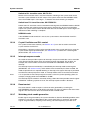
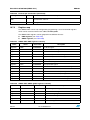
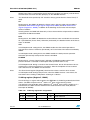
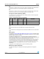
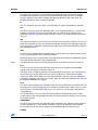
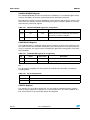
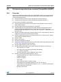
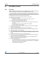
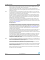
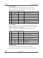
1.
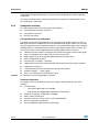
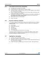
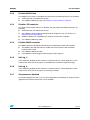
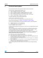
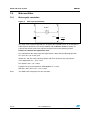
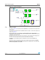
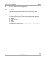
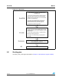
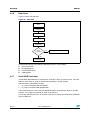
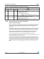
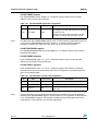
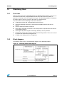
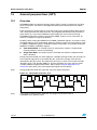
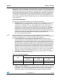
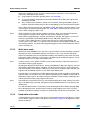
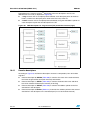
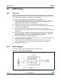
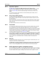
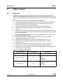
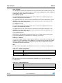
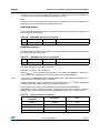
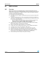
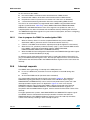
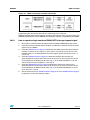
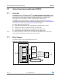
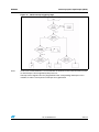
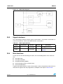
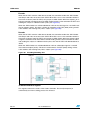
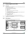
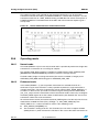
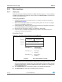
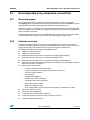
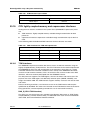
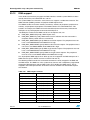
Clear the rst_n signal by driving it to ‘b0. All programmable registers will be cleared.
2.
Set the rst_n signal synchronously with the memory controller clock by driving the
signal to ’b1.
3.
Issue write register commands to configure the DRAM protocols and the settings for
the DCC. Keep the start parameter de-asserted during this initialization step.
4.
Assert the start parameter. This triggers the memory controller to execute the
initialization sequence using the parameters written into the registers.
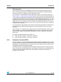
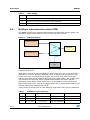
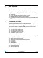
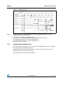
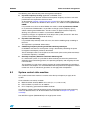
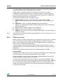
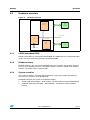
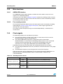
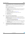
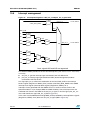
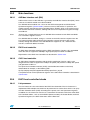
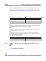
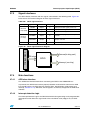
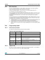
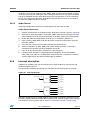
The memory controller will automatically initialize the DRAM memory devices and lock the
internal DCC. The DLL will process and send a signal to the initialization block when it has
locked.
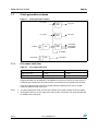
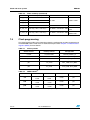
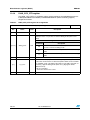
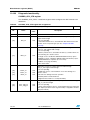
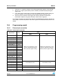
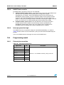
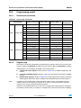
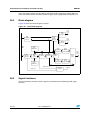
16.4
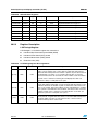
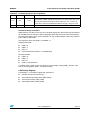
Programming model
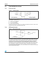
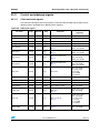
16.4.1
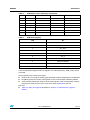
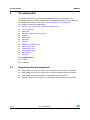
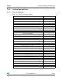
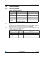
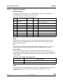
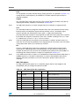
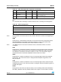
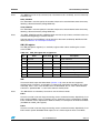
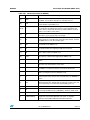
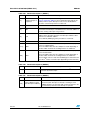
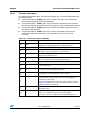
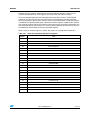
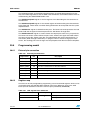
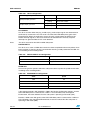
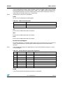
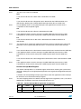
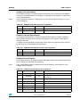
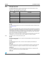
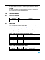
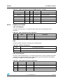
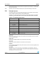
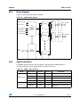
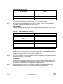
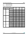
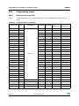
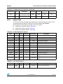
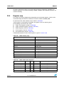
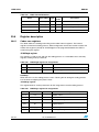
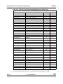
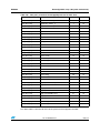
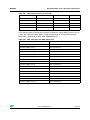
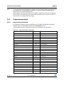
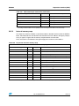
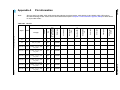
External pin connection
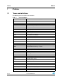
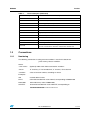
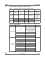
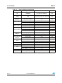
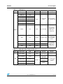
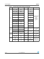
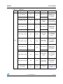
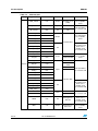
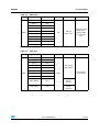
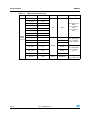
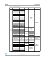
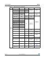
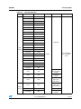
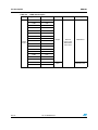
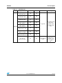
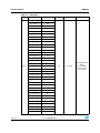
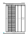
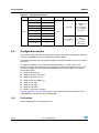
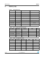
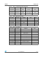
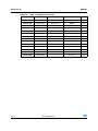
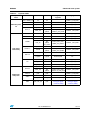
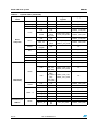
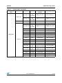
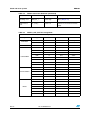
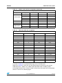
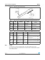
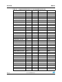
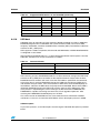
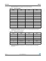
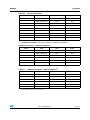
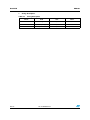
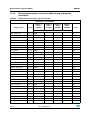
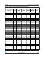
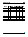
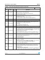
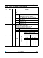
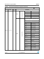
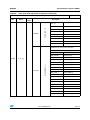
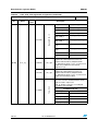
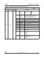
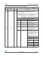
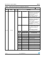
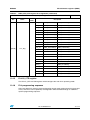
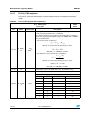
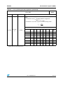
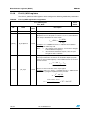
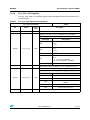
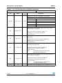
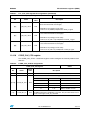
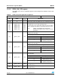
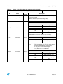
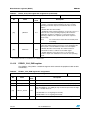
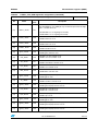
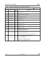
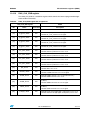
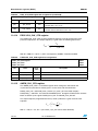
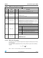
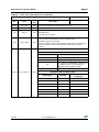
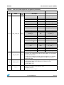
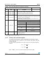
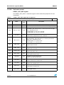
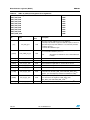
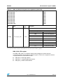
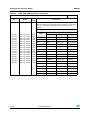
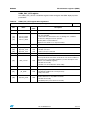
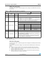
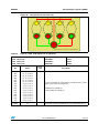
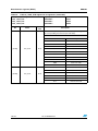
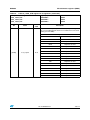
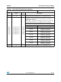
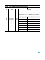
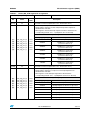
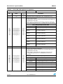
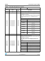
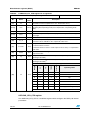
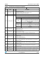
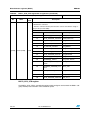
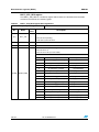
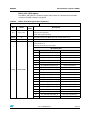
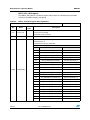
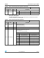
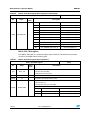
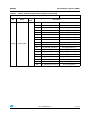
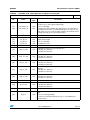
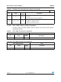
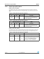
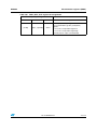
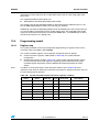
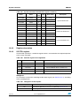
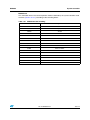
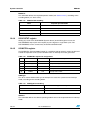
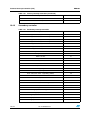
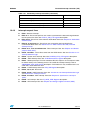
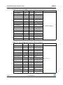
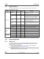
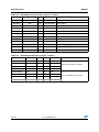
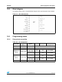
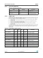
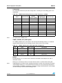
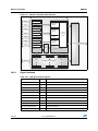
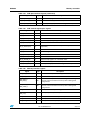
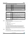
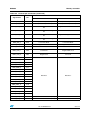
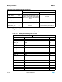
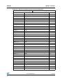
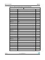
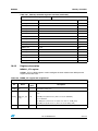
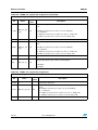
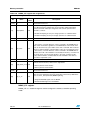
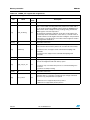
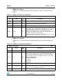
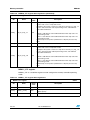
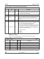
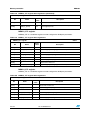
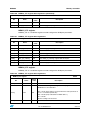
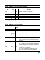
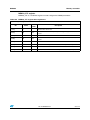
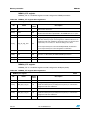
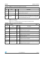
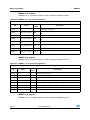
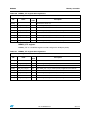
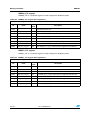
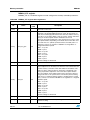
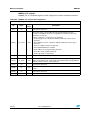
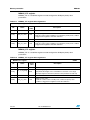
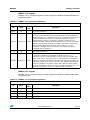
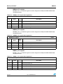
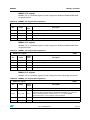
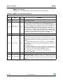
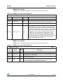
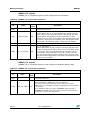
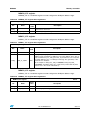
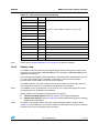
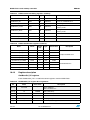
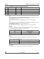
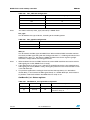
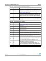
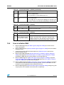
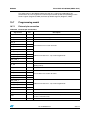
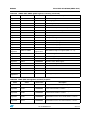
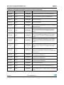
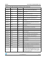
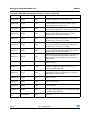
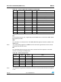
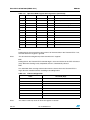
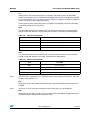
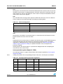
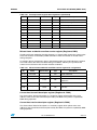
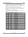
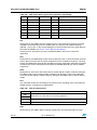
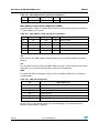
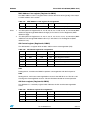
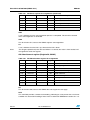
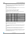
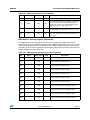
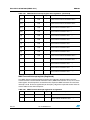
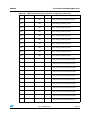
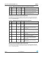
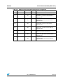
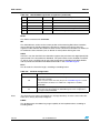
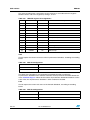
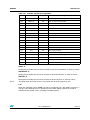
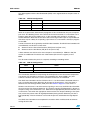
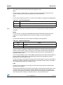
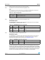
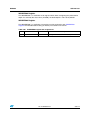
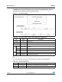
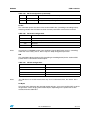
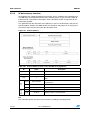
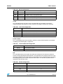
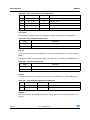
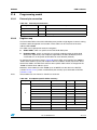
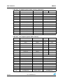
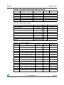
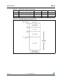
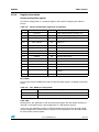
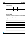
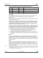
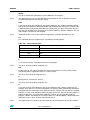
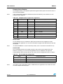
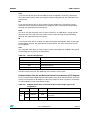
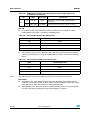
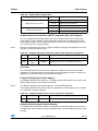
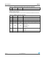
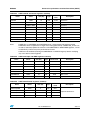
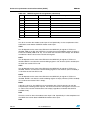
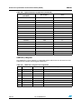
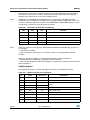
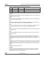
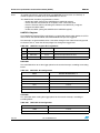
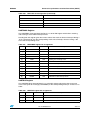
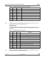
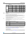
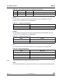
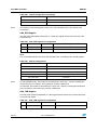
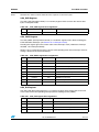
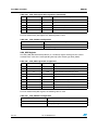
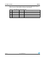
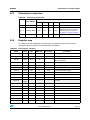
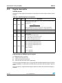
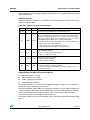
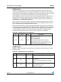
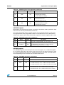
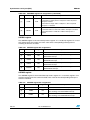
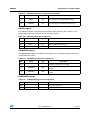
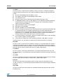
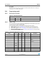
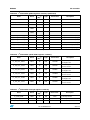
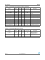
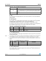
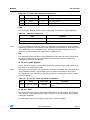
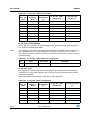
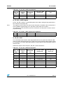
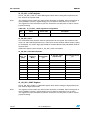
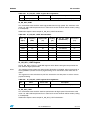
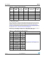
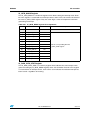
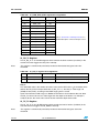
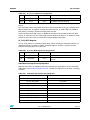
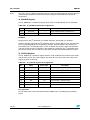
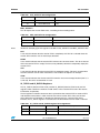
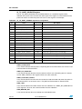
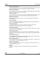
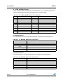
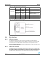
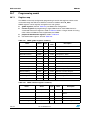
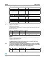
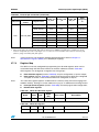
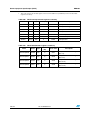
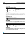
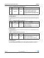
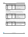
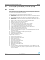
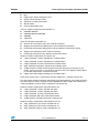
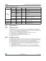
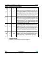
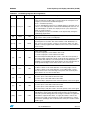
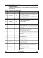
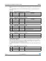
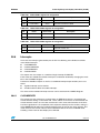
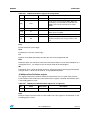
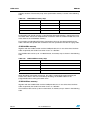
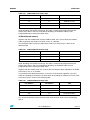
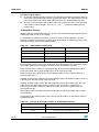
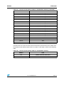
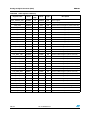
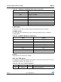
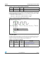
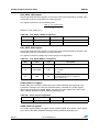
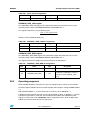
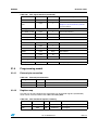
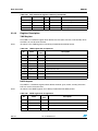
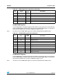
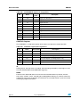
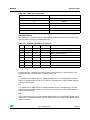
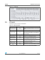
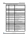
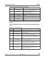
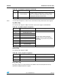
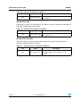
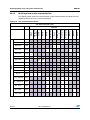
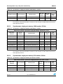
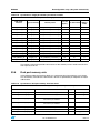
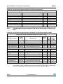
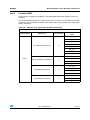
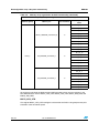
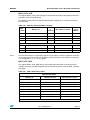
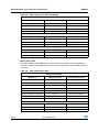
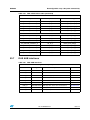
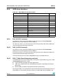
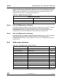
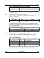
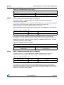
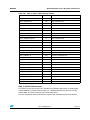
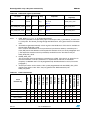
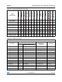
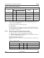
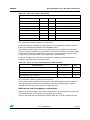
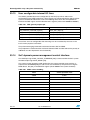
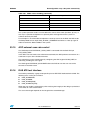
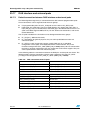
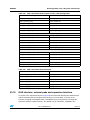
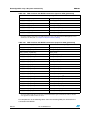
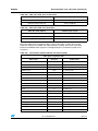
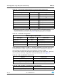
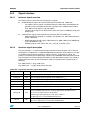
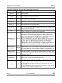
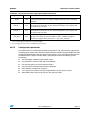
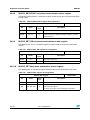
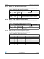
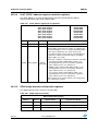
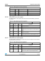
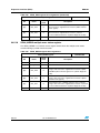
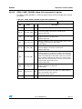
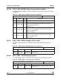
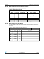
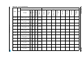
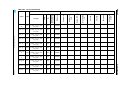
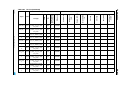
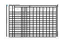
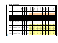
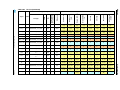
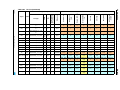
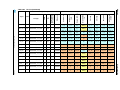
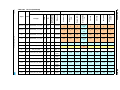
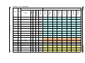
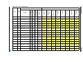
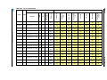
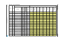
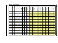
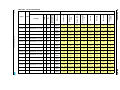
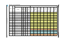
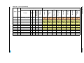
Table 164. External pin connection
Notes
Signal name
Pin
DDR2
DDR1
Address lines during the normal
operation. Data lines during the
Memory Modes register setting.
Address lines during the normal
operation. Data lines during the
Memory Modes register setting.
Bank addresses lines
Bank addresses lines
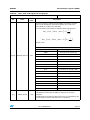
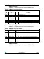
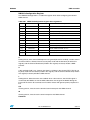
DDR_ADD_0
AB3
DDR_ADD_1
AB4
DDR_ADD_2
AA4
DDR_ADD_3
Y4
DDR_ADD_4
W4
DDR_ADD_5
W5
DDR_ADD_6
Y5
DDR_ADD_7
AA5
DDR_ADD_8
AB5
DDR_ADD_9
AB6
DDR_ADD_10
AA6
DDR_ADD_11
Y6
DDR_ADD_12
W6
DDR_ADD_13
W7
DDR_ADD_14
Y7
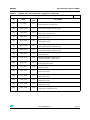
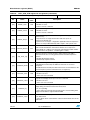
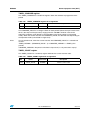
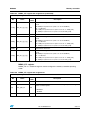
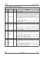
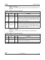
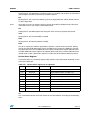
DDR_BA_0
Y9
DDR_BA_1
W9
DDR_BA_2
W10
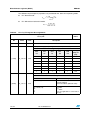
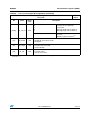
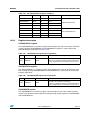
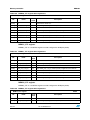
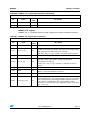
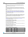
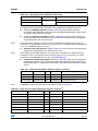
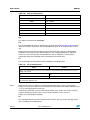
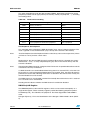
DDR_RAS
AB7
Row Address Strobe (active low)
Row Address Strobe (active low)
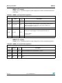
DDR_CAS
AA7
Column Address Strobe (active low)
Column Address Strobe (active low)
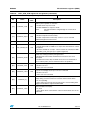
DDR_MEM_WE
AA8
Write Enable (active low)
Write Enable (active low)
236/712
Doc ID 022038 Rev 1