1
XC161-32 Derivatives
System Units (Vol. 1 of 2)
Memory Organization
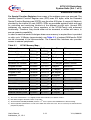
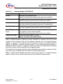
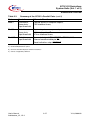
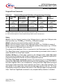
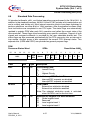
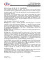
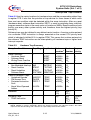
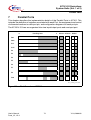
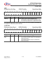
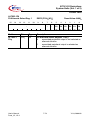
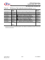
Field
Bits
Type
Description
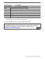
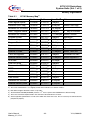
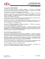
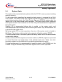
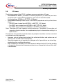
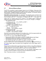
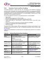
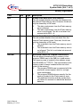
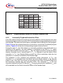
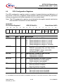
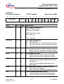
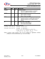
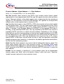
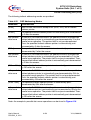
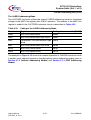
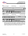
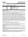
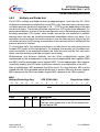
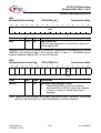
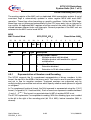
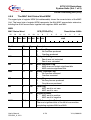
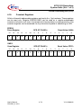
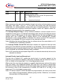
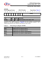
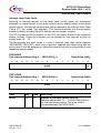
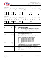
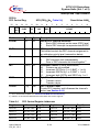
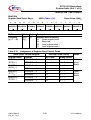
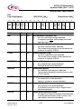
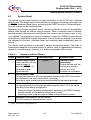
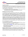
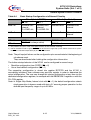
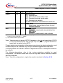
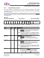
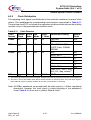
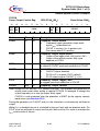
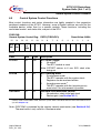
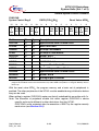
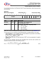
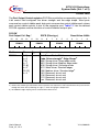
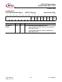
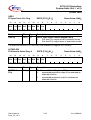
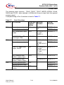
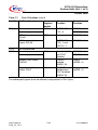
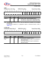
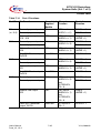
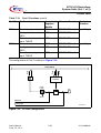
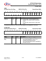
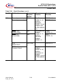
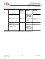
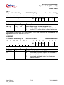
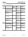
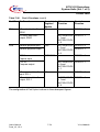
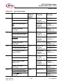
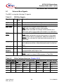
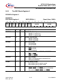
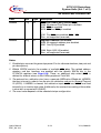
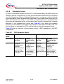
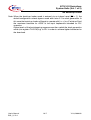
WSFLASH
[1:0]
rw
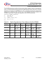
Wait States for the Flash Memory
This bitfield defines the number of additional wait
states, which are added for a read access from the
Flash memory area, which is located in the address
range from C0’0000H to DF’FFFFH.
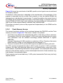
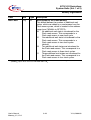
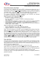
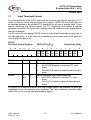
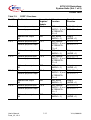
00
No additional wait state is introduced for the
Flash read access. This corresponds to a
Flash read access in one clock cycle.
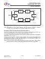
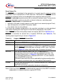
01
One additional wait state is introduced for the
Flash read access. This corresponds to a
Flash read access in two clock cycles.
(default)
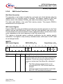
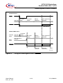
10
Two additional wait states are introduced for
the Flash read access. This corresponds to a
Flash read access in three clock cycles.
11
Three additional wait states are introduced for
the Flash read access. This corresponds to a
Flash read access in four clock cycles.
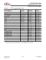
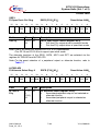
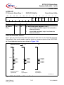
1) WSRAM selects the access timing for the standard PSRAM area. The access timing for the EPSRAM area
(F8’0000H) equals Flash accesses with WSFLASH = 00B.
User’s Manual
Memory_X1, V2.2
3-43
V1.0, 2004-02