1
Embedded Solutions
20P511-00 E1 – 2009-06-16
P511 – Dual Fast Ethernet
PMC
Configuration example
User Manual
®
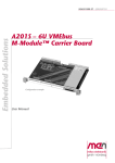
P511 - Dual Fast Ethernet PMC
P511 - Dual Fast Ethernet PMC
The P511 is a 32bit/33MHz PMC with dual Ethernet functionality. The two
channels can be accessed via two RJ45 connectors which are led to the front via an
adapter cable from a SCSI connector. They support half duplex and full duplex
operation.
The PMC offers the possibility to buffer all receive and transmit Ethernet frames
either in a local or in an external data buffer. This makes it possible to provide a
Worst Case Execution Time analysis which makes it particularly well suited for
safety-critical applications.
Up to 6 GPIO lines can be used on the module for additional functionality.
The P511 is based on the USM™ concept. USM™ Universal Submodules make
PMC modules more flexible than ever. The Ethernet functionality is realized via an
IP core implemented inside its on-board FPGA. This function can be changed at any
time through implementation of different IP cores. The corresponding line drivers
are realized on the USM™ which is simply plugged on the P511. One alternative
function is the combination of an Ethernet core with a fieldbus interface to build
gateways.
The module is suitable for any PMC compliant host carrier board in any type of bus
system, i.e. CPCI, VME or on any type of stand-alone SBC in telecommunication,
industrial, medical, transportation or aerospace applications. It offers long-term
availability for at least 10 years and is qualified for operation in the extended
temperature range.
MEN Mikro Elektronik GmbH
20P511-00 E1 – 2009-06-16
2
Technical Data
Technical Data
Ethernet Interface
• Two 10/100Base-T Ethernet channels
• Accessible on two RJ45 connectors via adapter cable
• Half duplex/full duplex support
Memory
• 32MB SDRAM memory
- Soldered
- DDR2
- 132MHz memory bus frequency
- FPGA-controlled
• 2MB non-volatile Flash
- For FPGA data and Nios® firmware
- FPGA-controlled
GPIO
• Up to six lines controlled via software
FPGA
• Standard factory FPGA configuration:
- Main bus interface
- Interrupt controller, SMBus controller
- 16Z087_ETH – Ethernet MAC IP core (2 IP cores for the 2 channels)
- 16Z043_SDRAM – SDRAM controller
- 16Z045_FLASH – Flash interface
- 16Z034_GPIO – GPIO controller
- The FPGA offers the possibility to add customized I/O functionality. See FPGA.
PMC Characteristics (PCI)
• Compliant with PCI Specification 2.2
• 32-bit/33-MHz, 3.3V V(I/O)
• Target and initiator
Peripheral Connections
• Via front panel on a shielded 50-pin HP D-Sub SCSI 2 receptacle connector
• Adapter cable to two RJ45 connectors included in the delivery
Electrical Specifications
• Isolation voltage:
- 1500 VAC
• Supply voltage/power consumption:
- +5V (-3%/+5%), 0.2W
- +3.3V (-5%/+5%), 0.46W
MEN Mikro Elektronik GmbH
20P511-00 E1 – 2009-06-16
3
Technical Data
Mechanical Specifications
• Dimensions: conforming to IEEE 1386.1
• Weight: 78g
Environmental Specifications
• Temperature range (operation):
- -40..+85°C (qualified components)
- Airflow: min. 1.0m/s
• Temperature range (storage): -40..+85°C
• Relative humidity (operation): max. 95% non-condensing
• Relative humidity (storage): max. 95% non-condensing
• Altitude: -300m to + 3,000m
• Shock: 15g/11ms
• Bump: 10g/16ms
• Vibration (sinusoidal): 1g/10..150Hz
• Conformal coating on request
MTBF
• tbd @ 40°C according to IEC/TR 62380 (RDF 2000)
Safety
• PCB manufactured with a flammability rating of 94V-0 by UL recognized manufacturers
EMC
• Conforming to EN 55022 (radio disturbance), IEC1000-4-2 (ESD) and
IEC1000-4-4 (burst)
Software Support
• Windows® (in preparation)
• Linux
• For more information on supported operating system versions and drivers see
online data sheet.
MEN Mikro Elektronik GmbH
20P511-00 E1 – 2009-06-16
4
Block Diagram
Block Diagram
Adapter cable to
two RJ45
Connectors
FPGA
Ethernet PHY
Transceivers
Ethernet MAC
Layer
GPIO Lines
GPIO Controller
50-pin front
connector
Memory
Controller
PCI
Interface
32-bit /
33-MHz
DDR2
SDRAM
32 MB
MEN Mikro Elektronik GmbH
20P511-00 E1 – 2009-06-16
5
Configuration Options
Configuration Options
CPU
• Nios® soft core implementation possible (e.g. for real-time Ethernet)
Rear I/O
• Via Pn4 rear I/O connector
Cooling
• Conduction Cooling
Please note that some of these options may only be available for large volumes.
Please ask our sales staff for more information.
For available standard configurations see online data sheet.
MEN Mikro Elektronik GmbH
20P511-00 E1 – 2009-06-16
6
FPGA
FPGA
Flexible Configuration
• This MEN board offers the possibility to add customized I/O functionality in
FPGA.
• It depends on the board type, pin counts and number of logic elements which IP
cores make sense and/or can be implemented. Please contact MEN for information on feasibility.
• You can find more information on our web page "User I/O in FPGA"
FPGA Capabilities
• FPGA Altera® Cyclone™ II EP2C35
- 33,216 logic elements
- 483,840 total RAM bits
- Supports Nios® II soft processor
• Connection
- Functions can be linked to Wishbone or Avalon® bus
- Available pin count: 46 pins (FPGA to USM™)
- Functions available via USM™ at front I/O connector
• MEN offers a USM™ development kit and an FPGA Development Package as
well as Flash update tools for different operating systems.
MEN Mikro Elektronik GmbH
20P511-00 E1 – 2009-06-16
7
Product Safety
Product Safety
!
Electrostatic Discharge (ESD)
Computer boards and components contain electrostatic sensitive devices.
Electrostatic discharge (ESD) can damage components. To protect the board and
other components against damage from static electricity, you should follow some
precautions whenever you work on your computer.
• Power down and unplug your computer system when working on the inside.
• Hold components by the edges and try not to touch the IC chips, leads, or circuitry.
• Use a grounded wrist strap before handling computer components.
• Place components on a grounded antistatic pad or on the bag that came with the
component whenever the components are separated from the system.
• Store the board only in its original ESD-protected packaging. Retain the original
packaging in case you need to return the board to MEN for repair.
MEN Mikro Elektronik GmbH
20P511-00 E1 – 2009-06-16
8
About this Document
About this Document
This user manual describes the hardware functions of the board, connection of
peripheral devices and integration into a system. It also provides additional
information for special applications and configurations of the board.
The manual does not include detailed information on individual components (data
sheets etc.). A list of literature is given in the appendix.
History
Issue
E1
Comments
First issue
Date of Issue
2009-06-16
Conventions
!
italics
bold
monospace
hyperlink
This sign marks important notes or warnings concerning proper functionality of the
product described in this document. You should read them in any case.
Folder, file and function names are printed in italics.
Bold type is used for emphasis.
A monospaced font type is used for hexadecimal numbers, listings, C function
descriptions or wherever appropriate. Hexadecimal numbers are preceded by "0x".
Hyperlinks are printed in blue color.
The globe will show you where hyperlinks lead directly to the Internet, so you can
look for the latest information online.
IRQ#
/IRQ
Signal names followed by "#" or preceded by a slash ("/") indicate that this signal is
either active low or that it becomes active at a falling edge.
in/out
Signal directions in signal mnemonics tables generally refer to the corresponding
board or component, "in" meaning "to the board or component", "out" meaning
"coming from it".
MEN Mikro Elektronik GmbH
20P511-00 E1 – 2009-06-16
9
About this Document
Legal Information
MEN Mikro Elektronik reserves the right to make changes without further notice to any products herein. MEN makes no
warranty, representation or guarantee regarding the suitability of its products for any particular purpose, nor does MEN assume
any liability arising out of the application or use of any product or circuit, and specifically disclaims any and all liability,
including without limitation consequential or incidental damages.
"Typical" parameters can and do vary in different applications. All operating parameters, including "Typicals" must be
validated for each customer application by customer's technical experts.
MEN does not convey any license under its patent rights nor the rights of others.
Unless agreed otherwise, MEN products are not designed, intended, or authorized for use as components in systems intended
for surgical implant into the body, or other applications intended to support or sustain life, or for any other application in which
the failure of the MEN product could create a situation where personal injury or death may occur. Should Buyer purchase or
use MEN products for any such unintended or unauthorized application, Buyer shall indemnify and hold MEN and its officers,
employees, subsidiaries, affiliates, and distributors harmless against all claims, costs, damages, and expenses, and reasonable
attorney fees arising out of, directly or indirectly, any claim of personal injury or death associated with such unintended or
unauthorized use, even if such claim alleges that MEN was negligent regarding the design or manufacture of the part.
Unless agreed otherwise, the products of MEN Mikro Elektronik are not suited for use in nuclear reactors or for application in
medical appliances used for therapeutical purposes. Application of MEN products in such plants is only possible after the user
has precisely specified the operation environment and after MEN Mikro Elektronik has consequently adapted and released the
product.
ESM™, ESMini™, MDIS™, MDIS4™, MENMON™, M-Module™, M-Modules™, SA-Adapter™, SA-Adapters™,
UBox™, USM™ and the MBIOS logo are trademarks of MEN Mikro Elektronik GmbH. PC-MIP® is a registered trademark
of MEN Micro, Inc. and SBS Technologies, Inc. MEN Mikro Elektronik®, ESMexpress® and the MEN logo are registered
trademarks of MEN Mikro Elektronik GmbH.
COM Express™ is a trademark of PCI Industrial Computer Manufacturers Group. CompactPCI® is a registered trademark of
PCI Industrial Computer Manufacturers Group. Microsoft® and Windows® are registered trademarks of Microsoft Corp.
Windows® Vista™ is a trademark of Microsoft Corp. PXI™ is a trademark of National Instruments Corp. QNX® is a
registered trademark of QNX Ltd. Tornado® and VxWorks® are registered trademarks of Wind River Systems, Inc.
All other products or services mentioned in this publication are identified by the trademarks, service marks, or product names
as designated by the companies who market those products. The trademarks and registered trademarks are held by the
companies producing them. Inquiries concerning such trademarks should be made directly to those companies. All other brand
or product names are trademarks or registered trademarks of their respective holders.
Information in this document has been carefully checked and is believed to be accurate as of the date of publication; however,
no responsibility is assumed for inaccuracies. MEN Mikro Elektronik accepts no liability for consequential or incidental
damages arising from the use of its products and reserves the right to make changes on the products herein without notice to
improve reliability, function or design. MEN Mikro Elektronik does not assume any liability arising out of the application or
use of the products described in this document.
Copyright © 2009 MEN Mikro Elektronik GmbH. All rights reserved.
Please recycle
Germany
MEN Mikro Elektronik GmbH
Neuwieder Straße 5-7
90411 Nuremberg
Phone +49-911-99 33 5-0
Fax +49-911-99 33 5-901
E-mail [email protected]
www.men.de
MEN Mikro Elektronik GmbH
20P511-00 E1 – 2009-06-16
France
MEN Mikro Elektronik SA
18, rue René Cassin
ZA de la Châtelaine
74240 Gaillard
Phone +33 (0) 450-955-312
Fax +33 (0) 450-955-211
E-mail [email protected]
www.men-france.fr
USA
MEN Micro, Inc.
24 North Main Street
Ambler, PA 19002
Phone (215) 542-9575
Fax (215) 542-9577
E-mail [email protected]
www.menmicro.com
10
Contents
Contents
1 Getting Started . . . . . . . . . . . . . . . . . . . . . . . . . . . . . . . . . . . . . . . . . . . . . . . .
1.1 Map of the Board. . . . . . . . . . . . . . . . . . . . . . . . . . . . . . . . . . . . . . . . .
1.2 Integrating the Board into a System . . . . . . . . . . . . . . . . . . . . . . . . . .
1.3 Installing Driver Software . . . . . . . . . . . . . . . . . . . . . . . . . . . . . . . . . .
14
14
15
15
2 Connecting the PMC Module . . . . . . . . . . . . . . . . . . . . . . . . . . . . . . . . . . . .
2.1 Peripheral Interfaces . . . . . . . . . . . . . . . . . . . . . . . . . . . . . . . . . . . . . .
2.1.1
Standard Version . . . . . . . . . . . . . . . . . . . . . . . . . . . . . . . . . .
2.1.2
Conduction Cooled Version (Optional). . . . . . . . . . . . . . . . .
2.2 Host PCI Interface . . . . . . . . . . . . . . . . . . . . . . . . . . . . . . . . . . . . . . . .
16
16
16
17
19
3 Functional Description . . . . . . . . . . . . . . . . . . . . . . . . . . . . . . . . . . . . . . . . . .
3.1 Power Supply. . . . . . . . . . . . . . . . . . . . . . . . . . . . . . . . . . . . . . . . . . . .
3.2 Memory . . . . . . . . . . . . . . . . . . . . . . . . . . . . . . . . . . . . . . . . . . . . . . . .
3.2.1
DRAM System Memory . . . . . . . . . . . . . . . . . . . . . . . . . . . .
3.2.2
Flash . . . . . . . . . . . . . . . . . . . . . . . . . . . . . . . . . . . . . . . . . . .
3.3 Ethernet Interfaces. . . . . . . . . . . . . . . . . . . . . . . . . . . . . . . . . . . . . . . .
3.3.1
Ethernet MAC Addresses . . . . . . . . . . . . . . . . . . . . . . . . . . .
3.3.2
Ethernet Status LEDs . . . . . . . . . . . . . . . . . . . . . . . . . . . . . .
3.3.3
Connection . . . . . . . . . . . . . . . . . . . . . . . . . . . . . . . . . . . . . .
3.3.4
General . . . . . . . . . . . . . . . . . . . . . . . . . . . . . . . . . . . . . . . . .
3.3.5
10Base-T . . . . . . . . . . . . . . . . . . . . . . . . . . . . . . . . . . . . . . . .
3.3.6
100Base-T . . . . . . . . . . . . . . . . . . . . . . . . . . . . . . . . . . . . . . .
3.4 GPIO . . . . . . . . . . . . . . . . . . . . . . . . . . . . . . . . . . . . . . . . . . . . . . . . . .
21
21
21
21
21
21
22
22
24
25
25
25
26
4 FPGA . . . . . . . . . . . . . . . . . . . . . . . . . . . . . . . . . . . . . . . . . . . . . . . . . . . . . . . . 27
4.1 FPGA Configuration Table . . . . . . . . . . . . . . . . . . . . . . . . . . . . . . . . . 28
5 Appendix . . . . . . . . . . . . . . . . . . . . . . . . . . . . . . . . . . . . . . . . . . . . . . . . . . . . .
5.1 PCI Configuration . . . . . . . . . . . . . . . . . . . . . . . . . . . . . . . . . . . . . . . .
5.2 Literature and Web Resources . . . . . . . . . . . . . . . . . . . . . . . . . . . . . . .
5.3 Finding out the Board’s Article Number, Revision and
Serial Number . . . . . . . . . . . . . . . . . . . . . . . . . . . . . . . . . . . . . . . . . . .
MEN Mikro Elektronik GmbH
20P511-00 E1 – 2009-06-16
29
29
29
29
11
Figures
Figure 1.
Figure 2.
Figure 3.
Figure 4.
Figure 5.
MEN Mikro Elektronik GmbH
20P511-00 E1 – 2009-06-16
Map of the board – bottom view (standard version) . . . . . . . . . . . . . . 14
Map of the board – bottom view (optional conduction cooled version) 14
Position of Ethernet status LEDs . . . . . . . . . . . . . . . . . . . . . . . . . . . . . 23
Block Diagram . . . . . . . . . . . . . . . . . . . . . . . . . . . . . . . . . . . . . . . . . . . 28
Labels giving the board’s article number, revision and serial number. 29
12
Tables
Table 1.
Table 2.
Table 3.
Table 4.
Table 5.
Table 6.
Table 7.
Table 8.
Table 9.
MEN Mikro Elektronik GmbH
20P511-00 E1 – 2009-06-16
Pin assignment of 50-pin HP D-Sub front connector . . . . . . . . . . . . . .
Pin assignment of 64-pin plug connector Pn4 . . . . . . . . . . . . . . . . . . .
Signal mnemonics. . . . . . . . . . . . . . . . . . . . . . . . . . . . . . . . . . . . . . . . .
Pin assignment of 64-pin board-to-board connector Pn1 . . . . . . . . . . .
Pin assignment of 64-pin board-to-board connector Pn2 . . . . . . . . . . .
Ethernet status LEDs . . . . . . . . . . . . . . . . . . . . . . . . . . . . . . . . . . . . . .
Pin assignment of the 8-pin RJ45 Ethernet 10Base-T/100Base-T
connectors. . . . . . . . . . . . . . . . . . . . . . . . . . . . . . . . . . . . . . . . . . . . . . .
Signal mnemonics for Ethernet 10Base-T/100Base-TX interface . . . .
FPGA – Factory standard configuration table for P511 (preliminary).
16
17
18
19
20
22
24
24
28
13
Getting Started
1
Getting Started
This chapter gives an overview of the board and some hints for first installation in a
system.
1.1
Map of the Board
Figure 1. Map of the board – bottom view (standard version)
6 5 4
LEDs for Ethernet
interface 2
50-pin
HP D-Sub
SCSI 2
connector
PCI bus
connectors
Pn1
Pn2
3 2 1
LEDs for Ethernet
interface 1
FPGA
Components marked in gray are located on the top of the board
Figure 2. Map of the board – bottom view (optional conduction cooled version)
Secondary therm al interface
3 2 1
LEDs for Ethernet
interface 1
Primary thermal interface
Primary thermal interface
Pn1
6 5
4
LEDs for Ethernet
interface 2
Pn2
PCI bus
connectors
FPGA
Pn4
Secondary therm al interface
Com ponents m arked in gray are located on the top of the board
MEN Mikro Elektronik GmbH
20P511-00 E1 – 2009-06-16
14
Getting Started
1.2
Integrating the Board into a System
You can use the following "check list" to install the PMC on a carrier board for the
first time and to test proper functioning of the board.
; Power-down the system and remove the PMC carrier board.
; Install the PMC in a suitable front-panel slot of the carrier board as described in
the carrier board’s user manual.
; Insert the carrier board into the system again.
; Power-up the system.
; If there is a system crash or other abnormal behavior at start-up, check if the
PMC is plugged properly.
; You can now install driver software for the P511.
1.3
Installing Driver Software
For a detailed description on how to install driver software please refer to the
respective documentation.
You can find any driver software available for download on MEN’s website.
MEN Mikro Elektronik GmbH
20P511-00 E1 – 2009-06-16
15
Connecting the PMC Module
2
Connecting the PMC Module
2.1
Peripheral Interfaces
2.1.1
Standard Version
Peripherals can only be connected via the 50-pin half-pitch D-Sub connector.
Connector types:
• 50-pin half-pitch D-Sub receptacle with latch block, 1.27 mm pitch
• Mating connector:
50-pin half-pitch D-Sub plug with latch, 1.27 mm pitch
Table 1. Pin assignment of 50-pin HP D-Sub front connector
1
25
MEN Mikro Elektronik GmbH
20P511-00 E1 – 2009-06-16
26
50
1
-
26
-
2
-
27
-
3
-
28
RX2-
4
-
29
RX2+
5
-
30
TX2-
6
-
31
TX2+
7
-
32
-
8
-
33
-
9
-
34
-
10
GPIO1
35
-
11
GPIO2
36
-
12
GPIO3
37
-
13
GPIO4
38
-
14
GPIO5
39
-
15
GPIO6
40
-
16
-
41
-
17
-
42
-
18
-
43
-
19
-
44
RX1-
20
-
45
RX1+
21
-
46
TX1-
22
-
47
TX1+
23
-
48
-
24
-
49
-
25
-
50
-
16
Connecting the PMC Module
2.1.2
Conduction Cooled Version (Optional)
Peripherals can only be connected via the 64-pin Pn4 rear I/O on-board connector.
Connector types:
• 64-pin SMT plug connector according to IEEE P1386
• Mating connector:
64-pin SMT receptacle connector according to IEEE P1386
Table 2. Pin assignment of 64-pin plug connector Pn4
1
GND
2
GND
3
GND
4
GND
5
6
7
8
9
10
RX2-
11
12
RX2+
13
14
TX2-
15
16
TX2+
18
GND
17
2
64
1
63
19
20
21
22
23
24
25
GPIO1
26
27
GPIO2
28
29
GPIO3
30
31
GND
32
33
GPIO4
34
35
GPIO5
36
37
GPIO6
38
39
40
41
42
43
44
45
MEN Mikro Elektronik GmbH
20P511-00 E1 – 2009-06-16
GND
GND
GND
46
GND
47
48
RX1-
49
50
RX1+
51
52
TX1-
53
54
TX1+
55
56
57
58
59
60
61
GND
62
GND
63
GND
64
GND
17
Connecting the PMC Module
Table 3. Signal mnemonics
Signal
Function
GND
-
Ground
GPIO[6:1]
in/out
General purpose input/output lines 1..6
RX1+/-
in
Differential pair of receive data lines, channel 1
TX1+/-
out
Differential pair of transmit data lines,
channel 1
RX2+/-
in
Differential pair of receive data lines, channel 2
TX2+/-
out
Differential pair of transmit data lines,
channel 2
MEN Mikro Elektronik GmbH
20P511-00 E1 – 2009-06-16
Direction
18
Connecting the PMC Module
2.2
Host PCI Interface
The P511 PMC supports the following signals of the 64-pin carrier board interface
connectors:
Table 4. Pin assignment of 64-pin board-to-board connector Pn1
2
64
MEN Mikro Elektronik GmbH
20P511-00 E1 – 2009-06-16
1
63
1
-
2
-
3
GND
4
INTA#
5
INTB#
6
INTC#
7
-
8
+5V
9
INTD#
10
-
11
GND
12
-
13
PCI-CLK
14
GND
15
GND
16
GNT[0]#
17
REQ[0]#
18
+5V
19
-
20
AD[31]
21
AD[28]
22
AD[27]
23
AD[25]
24
GND
25
GND
26
C/BE[3]#
27
AD[22]
28
AD[21]
29
AD[19]
30
+5V
31
-
32
AD[17]
33
FRAME#
34
GND
35
GND
36
IRDY#
37
DEVSEL#
38
+5V
39
GND
40
-
41
-
42
-
43
PAR
44
GND
45
-
46
AD[15]
47
AD[12]
48
AD[11]
49
AD[9]
50
+5V
51
GND
52
C/BE[0]#
53
AD[6]
54
AD[5]
55
AD[4]
56
GND
57
-
58
AD[3]
59
AD[2]
60
AD[1]
61
AD[0]
62
+5V
63
GND
64
-
19
Connecting the PMC Module
Table 5. Pin assignment of 64-pin board-to-board connector Pn2
2
64
1
63
1
-
2
-
3
-
4
-
5
-
6
GND
7
GND
8
-
9
-
10
-
11
-
12
+3.3V
13
RST#
14
-
15
+3.3V
16
-
17
-
18
GND
19
AD[30]
20
AD[29]
21
GND
22
AD[26]
23
AD[24]
24
+3.3V
25
IDSEL[0]
26
AD[23]
27
+3.3V
28
AD[20]
29
AD[18]
30
GND
31
AD[16]
32
C/BE[2]#
33
GND
34
-
35
TRDY#
36
+3.3V
37
GND
38
STOP#
39
PERR#
40
GND
41
+3.3V
42
SERR#
43
C/BE[1]#
44
GND
45
AD[14]
46
AD[13]
47
M66EN
48
AD[10]
49
AD[8]
50
+3.3V
51
AD[7]
52
-
53
+3.3V
54
-
55
-
56
GND
57
-
58
-
59
GND
60
-
61
-
62
+3.3V
63
GND
64
-
Connector types of Pn1 and Pn2:
• 64-pin SMT plug connector according to IEEE P1386
• Mating connector:
64-pin SMT receptacle connector according to IEEE P1386
MEN Mikro Elektronik GmbH
20P511-00 E1 – 2009-06-16
20
Functional Description
3
Functional Description
3.1
Power Supply
Power supply to the logic part is done via the carrier board (connectors Pn1/Pn2).
The necessary voltages are +5V and +3.3V.
3.2
Memory
3.2.1
DRAM System Memory
The board is equipped with 32 MB soldered DDR2 SDRAM memory, which is
controlled by the FPGA. The memory bus frequency is 132 MHz.
3.2.2
Flash
The board is equipped with 2 MB non-volatile Flash controlled by the FPGA.
3.3
Ethernet Interfaces
The P511 provides two Fast Ethernet interfaces which are controlled via two MEN
standard IP cores in the FPGA which are called 16Z087_ETH (see Chapter 4 FPGA
on page 27). They support full duplex operation and speed autonegotiation.
The Ethernet controllers can be configured in such a way that they can buffer all
receive and transmit Ethernet frames in the host memory (i.e. by transmitting the
frames via bus master DMA over PCI) or in the PMC local SDRAM memory.
The buffer memory (host memory or PMC local SDRAM memory) selection
depends on the highest address bit of the Wishbone Bus. This bit can be set in the
Transmit Buffer Location Register (TXBD_LOC) and the Receive Buffer Location
Register (RXBD_LOC) of the 16Z087_ETH IP core. You can find a detailed
description of these and the other registers in the IP core’s Reference Manual.
When the highest address bit of these registers are set to 1, the frames are stored in
the DDR2 memory. When the highest address bits are 0, the frames are stored in the
host memory.
MEN offers software which can control this function. See MEN’s website.
MEN Mikro Elektronik GmbH
20P511-00 E1 – 2009-06-16
21
Functional Description
3.3.1
!
Ethernet MAC Addresses
The MAC addresses of the Ethernet interfaces are stored in an onboard EEPROM.
The unique MAC addresses are set at the factory and should not be changed. Any
attempt to change these addresses may create node or bus contention and thereby
render the board inoperable. The MAC addresses on the P511 are:
00:C0:3A:9C:Cx:xx
• LAN1:
• LAN2:
00:C0:3A:9C:Dx:xx
where "00 C0 3A" is the MEN vendor code and "9C" is the MEN product code. The
last four digits depend on the interface and the serial number of the product.
The serial number is added to the offset, for example for LAN1:
• Serial number 0042: 0x xx xx = 0xC000 + 0x002A = 0x C0 2A
(See also Chapter 5.3 Finding out the Board’s Article Number, Revision and Serial
Number on page 29).
3.3.2
Ethernet Status LEDs
There are three status LEDs for each Ethernet channel which show the connection
speed, whether a link is established and whether there is transmit or receive activity.
See Table 6, Ethernet status LEDs on page 22 for the functionality of the LEDs.
See Figure 3, Position of Ethernet status LEDs on page 23 for their position.
Table 6. Ethernet status LEDs
LED
1
Connection speed of Ethernet interface 1
2
Link status of Ethernet interface 1
3
Receive/transmit activity of Ethernet interface 1
4
Connection speed of Ethernet interface 2
5
Link status of Ethernet interface 2
6
Receive/transmit activity of Ethernet interface 2
MEN Mikro Elektronik GmbH
20P511-00 E1 – 2009-06-16
Function
22
Functional Description
Figure 3. Position of Ethernet status LEDs
50-pin
HP D-Sub
SCSI 2
connector
6 5 4
LEDs for Ethernet
interface 2
3 2 1
LEDs for Ethernet
interface 1
FP
MEN Mikro Elektronik GmbH
20P511-00 E1 – 2009-06-16
23
Functional Description
3.3.3
Connection
The two Ethernet interfaces which are accessible at the 50-pin front connector can
be led to two RJ45 connectors via an adapter cable which is provided by MEN.
See MEN’s website for ordering information.
Connector types:
• Modular 8/8-pin mounting jack according to FCC68
• Mating connector:
Modular 8/8-pin plug according to FCC68
Table 7. Pin assignment of the 8-pin RJ45 Ethernet 10Base-T/100Base-T
connectors
1
1
TX+
2
TX-
3
RX+
4
-
5
-
6
RX-
7
-
8
-
8
Table 8. Signal mnemonics for Ethernet 10Base-T/100Base-TX interface
Signal
Function
RX+/-
in
Differential pair of receive data lines
TX+/-
out
Differential pair of transmit data lines
MEN Mikro Elektronik GmbH
20P511-00 E1 – 2009-06-16
Direction
24
Functional Description
3.3.4
General
Ethernet is a local-area network (LAN) protocol that uses a bus or star topology and
supports data transfer rates of 100 Mbits/s and more. The Ethernet specification
served as the basis for the IEEE 802.3 standard, which specifies the physical and
lower software layers. Ethernet is one of the most widely implemented LAN
standards.
Ethernet networks provide high-speed data exchange in areas that require
economical connection to a local communication medium carrying bursty traffic at
high-peak data rates.
A classic Ethernet system consists of a backbone cable and connecting hardware
(e.g. transceivers), which links the controllers of the individual stations via
transceiver (transmitter-receiver) cables to this backbone cable and thus permits
communication between the stations.
3.3.5
10Base-T
10Base-T is one of several adaptations of the Ethernet (IEEE 802.3) standard for
Local Area Networks (LANs). The 10Base-T standard (also called Twisted Pair
Ethernet) uses a twisted-pair cable with maximum lengths of 100 meters. The cable
is thinner and more flexible than the coaxial cable used for the 10Base-2 or
10Base-5 standards. Since it is also cheaper, it is the preferable solution for costsensitive applications.
Cables in the 10Base-T system connect with RJ45 connectors. A star topology is
common with 12 or more computers connected directly to a hub or concentrator.
The 10Base-T system operates at 10 Mbits/s and uses baseband transmission methods.
3.3.6
100Base-T
The 100Base-T networking standard supports data transfer rates up to 100 Mbits/s.
100Base-T is actually based on the older Ethernet standard. Because it is 10 times
faster than Ethernet, it is often referred to as Fast Ethernet. Officially, the 100Base-T
standard is IEEE 802.3u.
There are several different cabling schemes that can be used with 100Base-T, e.g.
100Base-TX, with two pairs of high-quality twisted-pair wires.
MEN Mikro Elektronik GmbH
20P511-00 E1 – 2009-06-16
25
Functional Description
3.4
GPIO
The P511 provides six GPIO lines which can be used as debug outputs, e.g. for
timing measurement in real-time Ethernet applications. The lines are controlled via
the 16Z034_GPIO IP core in the FPGA. See Chapter 4 FPGA on page 27.
The direction and state of each GPIO can be controlled and read by software.
MEN Mikro Elektronik GmbH
20P511-00 E1 – 2009-06-16
26
FPGA
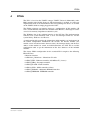
4
FPGA
The P511 is based on the USM™ concept. USM™ Universal Submodules make
PMC modules more flexible than ever. The functionality is realized via an IP core
implemented inside its on-board FPGA. The corresponding line drivers are realized
on the USM™ which is simply plugged on the P511.
The FPGA represents an interface between a configuration of I/O modules (IP
cores) and the PCI bus. The PCI core included in the FPGA is a PCI target. It can be
accessed via memory single/burst read/write cycles.
The Wishbone bus is the uniform interface to the PCI bus. The implementation
contains basic system functions such as reset and interrupt control etc. and the
system library, which are also IP cores.
A configuration table provides the information which modules are implemented in
the current configuration. Furthermore the revision, the instance number (one
module can be instantiated more than one time), the interrupt routing and the base
address of the module are stored. At initialization time, the CPU has to read the
configuration table to get the information of the base addresses of the included
modules.
The factory FPGA configuration for the standard P511 comprises the following
FPGA IP cores:
•
•
•
•
•
•
•
•
Main bus interface
16Z024-01_Chameleon – Chameleon V2 table
16Z087_ETH – Ethernet controller (10/100Base-T) (2 cores)
16Z052_GIRQ – Interrupt controller
16Z045_FLASH – Flash controller
16Z034_GPIO – GPIO controller (6 lines)
16Z043_SDRAM – Additional SDRAM controller
16Z084_IDEPROM - EEPROM controller
MEN Mikro Elektronik GmbH
20P511-00 E1 – 2009-06-16
27
FPGA
Figure 4. Block Diagram
FPGA
Wishbone Bus
16Z052_GIRQ
Interrupt controller
16Z043_DDR2
SDRAM controller
GPIO
16Z034_GPIO
GPIO controller 0
16Z084_IDEPROM
ID EEPROM
Controller
PCI bus
16Z014_PCI
PCI-to-Wishbone
16Z001_SMB
SMBus controller
Configuration
CPLD
Chameleon table
V2
16Z087_ETH
Ethernet Controller
Ethernet PHY
Flash
16Z045_FLASH
Flash interface
16Z087_ETH
Ethernet Controller
Ethernet PHY
1 LED is used to
indicate correct FPGA
configuration
4.1
DDR2 SDRAM
EEPROM
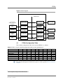
FPGA Configuration Table
The resulting configuration table of the standard FPGA is as follows:
Table 9. FPGA – Factory standard configuration table for P511 (preliminary1)
IP Core
Chameleon Table
16Z045_FLASH
16Z001_SMB
16Z034_GPIO
16Z084_IDEPROM
16Z052_GIRQ
16Z043_SDRAM
16Z087_ETH
16Z087_ETH
Device Variant Revision Interrupt Group Instance
24
1
11
3F
0
0
45
1
4
3F
0
0
1
0
8
0
0
0
34
0
10
1
0
0
84
0
2
3F
0
0
52
0
6
3F
0
0
43
1
9
3F
0
0
87
0
6
2
0
0
87
0
6
3
0
1
BAR
0
0
0
0
0
0
1
2
3
Offset
0
100
200
300
400
500
0
0
0
Size
100
100
100
100
100
100
2E+06
1000
1000
For a detailed description of the IP Cores please see the respective IP Core reference
manuals.
1
There might be changes in the table in the future
MEN Mikro Elektronik GmbH
20P511-00 E1 – 2009-06-16
28
Appendix
5
Appendix
5.1
PCI Configuration
The P511 has the following IDs on the PCI bus:
•
•
•
•
PCI Device ID: 0x4D45
PCI Vendor ID: 0x1172
Subsystem Device ID: 0x5A14
Subsystem Vendor ID: 0x006F
5.2
Literature and Web Resources
• P511 data sheet with up-to-date information and documentation:
www.men.de/products/15P511-.html
5.3
Finding out the Board’s Article Number, Revision and
Serial Number
MEN user documentation may describe several different models and/or hardware
revisions of the P511. You can find information on the article number, the board
revision and the serial number on two labels attached to the board.
• Article number: Gives the board’s family and model. This is also MEN’s ordering number. To be complete it must have 9 characters.
• Revision number: Gives the hardware revision of the board.
• Serial number: Unique identification assigned during production.
If you need support, you should communicate these numbers to MEN.
Figure 5. Labels giving the board’s article number, revision and serial number
Complete article number
15P511-00
00.00.00
Revision number
Serial number
MEN Mikro Elektronik GmbH
20P511-00 E1 – 2009-06-16
29
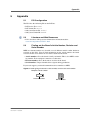
You can request the circuit diagrams for the current revision of the product described in this manual by
completely filling out and signing the following non-disclosure agreement.
Please send the agreement to MEN by mail. We will send you the circuit diagrams along with a copy of
the completely signed agreement by return mail.
®
MEN reserves the right to refuse sending of confidential information for any reason that MEN may consider substantial.
Non-Disclosure Agreement
for Circuit Diagrams provided by MEN Mikro Elektronik GmbH
between
MEN Mikro Elektronik GmbH
Neuwieder Straße 5-7
D-90411 Nürnberg
(”MEN”)
and
____________________
____________________
____________________
____________________
(”Recipient”)
We confirm the following Agreement:
MEN
Recipient
Date:
______________________
Date:
______________________
Name:
______________________
Name:
______________________
Function:
______________________
Function:
______________________
Signature:
Signature:
____________________________________
____________________________________
MEN Mikro Elektronik GmbH
Neuwieder Straße 5-7
90411 Nürnberg
Deutschland
The following Agreement is valid as of the date of the MEN signature.
Tel. +49-911-99 33 5-0
Fax +49-911-99 33 5-901
Non-Disclosure Agreement for Circuit Diagrams page 1 of 2
E-Mail [email protected]
www.men.de
1
Subject
The subject of this Agreement is to protect all information contained in the circuit diagrams of the following product:
®
Article Number: __________________ [filled out by recipient]
MEN provides the recipient with the circuit diagrams requested through this Agreement only for information.
2
Responsibilities of MEN
Information in the circuit diagrams has been carefully checked and is believed to be accurate as of the
date of release; however, no responsibility is assumed for inaccuracies. MEN will not be liable for any
consequential or incidental damages arising from reliance on the accuracy of the circuit diagrams. The
information contained therein is subject to change without notice.
3
Responsibilities of Recipient
The recipient, obtaining confidential information from MEN because of this Agreement, is obliged to protect this information.
The recipient will not pass on the circuit diagrams or parts thereof to third parties, neither to individuals
nor to companies or other organizations, without the written permission by MEN. The circuit diagrams
may only be passed to employees who need to know their content. The recipient protects the confidential information obtained through the circuit diagrams in the same way as he protects his own confidential information of the same kind.
4
Violation of Agreement
The recipient is liable for any damage arising from violation of one or several sections of this Agreement.
MEN has a right to claim damages amounting to the damage caused, at least to €100,000.
5
Other Agreements
MEN reserves the right to pass on its circuit diagrams to other business relations to the extent permitted
by the Agreement.
Neither MEN nor the recipient acquire licenses for the right of lectual possession of the other party
because of this Agreement.
This Agreement does not result in any obligation of the parties to purchase services or products from the
other party.
6
Validity of Agreement
The period after which MEN agrees not to assert claims against the recipient with respect to the confidential information disclosed under this Agreement shall be _______ months [filled out by MEN]. (Not
less than twenty-four (24) nor more than sixty (60) months.)
7
General
If any provision of this Agreement is held to be invalid, such decision shall not affect the validity of the
remaining provisions and such provision shall be reformed to and only to the extent necessary to make
it effective and legal.
This Agreement is only effective if signed by both parties.
Amendments to this Agreement can be adopted only in writing. There are no supplementary oral agreements.
This Agreement shall be governed by German Law.
MEN Mikro Elektronik GmbH
The court of jurisdiction shall be Nuremberg.
Neuwieder Straße 5-7
90411 Nürnberg
Deutschland
Tel. +49-911-99 33 5-0
Fax +49-911-99 33 5-901
Non-Disclosure Agreement for Circuit Diagrams page 2 of 2
E-Mail [email protected]
www.men.de