1
Marcos Augusto Menezes Vieira
Orientador: Diógenes Cecílio da Silva
BEAN: Uma Plataforma Computacional
para Rede de Sensores Sem Fio
Dissertação apresentada ao Curso de Pósgraduação em Ciência da Computação da
Universidade Federal de Minas Gerais, como
requisito parcial para a obtenção do grau de
Mestre em Ciência da Computação.
Belo Horizonte
15 de Abril de 2004
UNIVERSIDADE FEDERAL DE MINAS GERAIS
FOLHA DE APROVAÇÃO
Plataforma Computacional para Rede de Sensores Sem Fio
MARCOS AUGUSTO MENEZES VIEIRA
Dissertação defendida e aprovada pela banca examinadora constituída pelos Senhores:
P
E
CR - Orientador
EE - UFMG
P
E
JREIRO
;ão - UFMG
P
E
:ão - UFMG
Prof. Claudionor José Nunes Coelho Júnior
Departamento de Ciência da Computação - UFMG
Profa ]
Bea^ys Ruiz
Departamento de Informática - PUC - PR
Belo Horizonte, 15 de abril de 2004.
Resumo
Redes de Sensores Sem Fio (RSSFs) são redes corri gránde número de micro-sensores compactos com
capacidade de comunicação sem fio, chamados de nós sensores. Uma RSSF tem o potencial para um
grande numero de aplicações, que varia desde coletar dados do meio-ambiente até aplicações militares. O objetivo deste trabalho é projetar uma plataforma computacional, chamada BEAN {Brazilian
Energy-Efficient Architectural Node), que inclui componentes de hardware e software, e servirá de
protótipo para uma RSSF. Desafios na arquitetura como poder computacional, consumo de energia,
fontes de energia, canais de comunicação e capacidade de sensoriar são impostos aos projetistas. Em
nosso conhecimento, BEAN é o primeiro nó sensor que permite medir o consumo de energia de cada
componente e também o primeiro protótipo projetado no Brasil.
Abstract
Wireless sensor networks are networks of large quantities of compact micro-sensors with wireless
communication capability, called sensor nodes. Emerging applications of data gathering range from
the environmental to the military. The objective of this work is to project a computer platform, called
BEAN (Brazilian Energy-Efficient Architectural Node), that includes software and hardware components, which will be a prototype device for wireless sensor networks.Architectural challenges are
posed for designers such as computational power, energy consumption, energy sources, communication channels and sensing capabilities. In our knowledge, BEAN is the first sensor node that allow
measuring the power consumption of each component and it is the first sensor node prototype designed in Brazil.
Agradecimentos
É muito difícil mencionar aqui todas as pessoas que têm me apoiado durante este tempo.
Aos meus pais, Heloísa Beatriz e José Augusto, pelo esforço para que me proporcionassem uma
boa formação e educação. Aos meus irmãos Alessandra e Luiz Filipe, que sempre estiveram por
perto.
Ao Prof. Diógenes por todo apoio que me deu, pela amizade, pela paciência, pelas idéias e pelos
ensinamentos que sempre me passou.
Ao Prof. Antonio Otávio, pelo apoio desde o início, quando eu ainda era aluno de graduação, pela
amizade e consideração.
Aos professores e funcionários do DCC, em especial aos professores A. Alfredo, Claudionor,
Linnyer, Newton, Mário, pelos ensinamentos e sugestões que contribuíram para a minha formação.
Aos meus amigos de graduação da Turma 98, membros da Pov^^ertec®, amigos do Laboratório
Engetron e LECOM, especialmente Gustavo (gms), Alex, Cadu, Romeo, Daniela, Breno Vitorino,
Vinícius (Makish), Otaviano, Ajmendes, Valdeci, Felipe, Maia, pela amizade.
A equipe de desenvolvimento César e Rangel.
s j
A vitoriosa equipe ACM pelo esforço e dedicação.
Aos membros do OSV e Bier e organizadores do álbum de figurinhas, pelos momentos de lazer.
A todos os outros amigos, como o Nacif, Ana, Tom, Rafael, Bruno, Márcia, Lidia.
Ao PNM (Programa Nacional de Microeletrônica) (processo 13.3555/2002-0), pela bolsa de estudos, à Texas Instruments do Brasil pelo kit de desenvolvimento e amostras e ao projeto Sensomet
(55 2111/02-3) pelo apoio financeiro parcial.
Finalmente, à Ciência e ao glorioso Clube Atlético Mineiro.
i
Contents
List of Figures
^
List of Tables
vm
Breve Resumo da Dissertação em Português
1
Introduction
^
1.1
WSN Architecture
2
1.2
Embedded System
2
1.3
Objective and Motivation
3
1.4
Text Organization
4
2
Related Work
3
Sensor Node Architecture
4
g
3.1
WSN Components
14
3.2
Sensor node functional components
15
3.2.1
Processing Block
16
3.2.2
Sensing Block
16
3.3
Characteristics and Requirements
17
3.4
Challenges
Ig
BEAN Hardware Components
20
4.1
Processing Unit
20
4.1.1
21
Programmable Logic
ii
CONTENTS
—
4.2
4.1.2
Microcontrollers
22
4.1.3
Texas Instruments MSP430
25
Power
4.2.1
4.3
4.4
4.5
4.6
4.7
5
ni
22
Batteries
22
Communication
24
4.3.1
Laser communication
34
4.3.2
Infrared
25
4.3.3
Radio-frequency (RP)
25
Sensing Unit
^2
4.4.1
^2
Sensor Bus
Other components
4.5.1
Extended memory
44
4.5.2
Debugging
4.7
4.5.3
Serial Number
4^
4.5.4
Real Time Clock
4g
4.5.5
Measuring Energy
4ç
Interfacing CC1000 and MSP430
50
4.6.1
CC 1000 Application Circuit
50
4.6.2
Interfacing Radio and the Microcontroller
50
4.6.3
CCIOOOPP
55
4.6.4
Radio Connector
57
Project Decisions
57
BEAN^PI
gQ
5.1
gj
Drivers
5.1.1
SPI Driver
^2
5.1.2
1-Wire Driver
^4
5.1.3
LED Driver
5.1.4
Queue Driver
5.1.5
Memory Driver
5.1.6
Radio Driver
gy
CONTENTS
5.1.7
5.2
6
7
Case Study
*70
Development Tools
70
Energy issues
«74
6.1
Background
74
6.1.1
Battery behavior
76
6.1.2
Radio Energy Model
76
6.2
CMOS technology
7g
6.3
Energy Management Techniques
79
6.4
Low Power X Energy-Efficiency
gO
6.5
Memory
6.6
Power Budget
Final Considerations
gg
7.1
Conclusion
g6
7.2
Future Work
gg
7.2.1
Sensor boards
gg
7.2.2
Radio
gg
7.2.3
BEANJSJ>I
gg
7.2.4
New Platforms
90
References
A Schematic
B
gj
92
]^q2
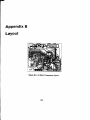
Layout
C API
107
C.l
Clock
207
C.2
LED
JQ7
C.3
Memory
^07
C.4
1-Wire
108
C.5
Radio
109
CONTENTS
C.6
SPI
109
C.7
Queue
1^0
D Radio Board
E Bill of Materials
F
V
Glossary
List of Figures
1
Rede de Sensores Sem Fio
2
Diagrama de Blocos do Protótipo do Nó Sensor
3
API
1.1
Wireless sensor network
2.1
EYES
^2
2.2
Medusa2
j2
2.3
Mica
12
2.4
Mica2 and Mica2-dot
j2
2.5
PushPin
12
2.6
WecMote
22
2.7
Telos
22
2.8
yuamp
22
2.9
WINS
23
All
xiv
2
2.10 BTnode
23
2.11 Nymph
23
2.12 ESB
23
2.13 Spec
22
3.1
Block Diagram of Sensor Node Prototype
15
3.2
System architecture and challenges of a sensor node
19
4.1
Typical Current Consumption vs. Operation Modes [93]
25
4.2
Register Overview [44]
26
VI
LISTOFnGURES
Vll
4.3
Low-Power CPU [44]
26
4.4
Functional block diagram of MSP430xx 16x [44]
27
4.5
Frequency versus Supply Voltage [44]
28
4.6
Pin Designation [45]
29
4.7
Different modulation for RF [48]
35
4.8
I/Q phases of 0-QPSK [18]
37
4.9
Ratio of receiver packet per distance for TRIOOO and CCIOOO components [47]. ...
38
4.10 Rayleigh fading [47]
4.11 M25P40[60]
4^
4.12 DS2417 [27]
4.13 A new methodology to evaluate on-the-fly the power consumption of WSN algorithms. 49
4.14 CCIOOO Application Circuit [16]
5q
4.15 CCIOOO-MCU Hardware Interface [96]
4.16 SPI Configuration Interface [96]
52
4.17 SPI data Interface [96].
53
4.18 Connection MCU USART Modules to other BEAN Components
54
4.19 Different encoding strategies [16]
55
4.20 Programmable output power allows changing radio range
56
4.21 CC1000PP[17]
5.1
BEAN_API
gj
5.2
MSP430 USART as Master, External Device With SPI as Slave [93]
63
5.3
MSP430 USART as Slave in Three-Pin or Four-Pin Configuration [93]
64
5.4
1-Wire waveforms [24]
65
5.5
Queue
5.6
Read Data Bytes (READ) Instruction Sequence and Data-Out Sequence [60]
5.7
Radio driver using SPI
5.8
Radio Driver using State Machine [19]
70
6.1
Current per unit time of a set of tasks
75
6.2
Radio Model
jj
6.3
Memory Current Consumption at Standby and Down Mode
82
69
LIST OF FIGURES
6.4
BEAN Savings
7.1
BEANboai'd
A.l
BEAN Schematic .
B. 1
All BEAN Components Layout
B.2
BEAN Bottom Layout
B.3
BEAN Top Layout
B.4
BEAN Components Layout
D. 1
Radio Board Bottom Layout
.
D.2 Radio Board Top Layout
D.3
Radio Board Schematic Layout
List of Tables
1
Orçamento energético do BEAN
2
Orçamento Energético do BEAN e do Mica2
3
Consumo em mA-hora
4
Capacidade da bateria em meses
5
Economia de BEAN
2.1
Sensor Node Platforms
jj
4.1
Microcontroller Comparison
24
4.2
MCU Port Mapping
29
4.2
MCU Port Mapping
3q
4.2
MCU Port Mapping
32
4.2
MCU Port Mapping
32
4.3
Comparison of energetic sources
33
4.4
Battery technology Comparison
33
4.5
Radio components
42
4.6
Sensor types specifications
43
4.7
Sensor bus comparison
45
4.8
Memory Comparison
4^
4.9
Memory Pin Description
45
W
xxi
'**•••
vví
••«••...
XXI
4.10 JTAG interface pin
4^
4.11 DS2417 Pin Description [27]
49
4.12 CClOOOPins
5j
4.13 Output power settings and typical current consumption at 868 Mhz
56
ix
LIST OF TABLES
4.14 Pin description of Radio Connector.
X
57
4.15 BEAN Overview
5.1
1-Wire Operations
5.2
Memory Instruction Set
gg
5.3
Development Tools
73
6.1
BEAN Power Budget
g2
6.2
Mica2 Power Budget
gg
6.3
Power budget of BEAN and Mica2
g4
6.4
Computed mA-hr
g^
6.5
Months per battery Capacity
g5
7.1
Sensor Node Prices
gg
7.2
MSP430F161X
90
E.l
Radio Board Components
E.2
Bean Components
Breve Resumo da Dissertação em
Português
1 Introdução
Redes de Sensores Sem Fio (RSSFs) são redes com grande número de micro-sensores compactos com
capacidade de comunicação sem fio, chamados de nós sensores. O objetivo destas redes é coletaidados. A disponibilidade de dispositivos sensores de baixo consumo, processadores embutidos e
circuitos integrados de comunicação está pernütindo o projeto de nós sensores. Figura 1 ilustra uma
RSSF. Cada ponto representa um nó sensor. Cada dispositivo sensoria o meio-ambiente, processa e
transmite os dados para um observador externo chamado de estação base.
Rede de Sensores Sem Fio tem o potencial para várias aplicações e algumas já são realidade,
por exemplo, em uma metrópole para monitorar tráfego e condições das ruas; em engenharia para
momtorar pontes e estruturas de prédios, em florestas para detecção de fogo [81]; na agricultura de
precisão, em serviços de recuperação de desastres;em serviços de manutenção como usinas nucleares
e na biomedicina [83].
O objetivo deste trabalho é projetar uma plataforma computacional, que inclui componentes de
hardware e software, que servirá de protótipo para rede de sensores sem fio. Este protótipo de nó
sensor será chamado Brazilian Energy-Efficient Architectural Node (BEAN).
Neste documento, as considerações de projeto e escolha de componentes para o protótipo de RSSF
serão discutidas. Um estudo dos nós sensores atuais é apresentado, investigando e analisando alguns
dos desafios de arquitetura impostos a estes dispositivos, incluindo uma pesquisa das plataformas
dos nós sensores e técnicas de gerência de energia. RSSF pode ser vista como um caso especial
de sistema embutido e se beneficiar do grande conhecimento já existente. Um estudo comparativo
xi
Breve Resumo da Dissertação em
Português
1 Introdução
Redes de Sensores Sem Fio (RSSFs) são redes com grande número de micro-sensores compactos com
capacidade de comunicação sem fio, chamados de nós sensores. O objetivo destas redes é coletaidados. A disponibilidade de dispositivos sensores de baixo consumo, processadores embutidos e
circuitos integrados de comunicação está permitindo o projeto de nós sensores. Figura 1 ilustra uma
RSSF. Cada ponto representa um nó sensor. Cada dispositivo sensoria o meio-ambiente, processa e
transmite os dados para um observador externo chamado de estação base.
Rede de Sensores Sem Fio tem o potencial para várias aplicações e algumas já são realidade,
por exemplo, em uma metrópole para monitorar tráfego e condições das ruas; em engenharia pai"a
monitorar pontes e estruturas de prédios, em florestas para detecção de fogo [81]; na agricultura de
precisão, em serviços de recuperação de desastres;em serviços de manutenção como usinas nucleares
e na biomedicina [83].
O objetivo deste trabalho é projetar uma plataforma computacional, que inclui componentes de
hardware e software, que servirá de protótipo para rede de sensores sem fio. Este protótipo de nó
sensor será chamado Brazilian Energy-Efficient Architectural Node (BEAN).
Neste documento, as considerações de projeto e escolha de componentes para o protótipo de RSSF
serão discutidas. Um estudo dos nós sensores atuais é apresentado, investigando e analisando alguns
dos desafios de arquitetura impostos a estes dispositivos, incluindo uma pesquisa das plataformas
dos nós sensores e técnicas de gerência de energia. RSSF pode ser vista como um caso especial
de sistema embutido e se beneficiar do grande conhecimento já existente. Um estudo comparativo
xi
Breve Resumo em Português
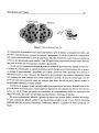
xii
Figura 1: Rede de Sensores Sem Fio.
de componentes de prateleira como microcontroladores, tipos de bateria, componentes de rádio, que
são muito importantes para o projeto do sistema, é apresentado. O foco do projeto é em componentes
individuais e não em detalhes a m'vel de subsistemas. Escolha do hardware, assim como as soluções de
software, são apresentadas neste trabalho. Uma API application programming interface bem definida,
que pode ser usada em outros projetos também é apresentada.
Um nó sensor é composto de unidade de potência, unidade de processamento, unidade de sensores,
e unidade de comunicação. A unidade de potência provê energia para o funcionamento do nó sensor.
A unidade de processamento é responsável por coletar e processar sinais capturados dos sensores e
tiansmiti-los para a rede. Sensores são dispositivos que produzem uma resposta mensurável dado
uma mudança em uma condição física como temperatura e pressão. O canal de comunicação sem fio
provê um meio para transmitir sinais dos sensores para dentro da rede ou para o mundo exterior e
também para estabelecer e manter a RSSF.
O consumo de energia é e será a primeira métrica no projeto de um nó sensor. Enquanto que existe
a Lei de Moore que prediz que a complexidade de dispositivos microeletrônicos dobra a cada dezoito
meses, e a Lei de Gilder, que prediz um crescimento de comportamento similar ao exponencial na
largura de banda, não existe uma predição equivalente para a tecnologia de baterias.
No nosso conhecimento, BEAN é o primeiro nó sensor que permite medir o consumo de energia
de cada componente. BEAN também é um dos primeiros projetos a usar o novo microcontrolador
MSP430F169 [93] da Texas Instruments. Finalmente, BEAN é o primeiro nó sensor projetado no
Brasil.
Breve Resumo em Português
xiii
As motivações principais para este trabalho são a necessidade de um protótipo de nó sensor paia
o projeto Sensomet [85] e também não existe uma plataforma computacional para RSSF no mercado
nacional brasileiro pois este é um tópico recente. Finalmente, é muito importante o desenvolvimento
da tecnologia, tendo conhecimento completo desde o hardware até o software. Como especificado no
documento do NSF [66], RSSF é uma das grande áreas de pesquisa atualmente.
2 Arquitetura do Nó Sensor
2.1 Características e Requisitos
Nesta seção, serão discutidas algumas características e requisitos do protótipo do nó sensor. Este
projeto não tem a intenção de projetar um dispositivo que será comparável a um nó sensor real.
Enquanto que um produto real tamanho e custo são requisitos essenciais, o foco deste projeto é em
um sistema fácil de expandir com um grande número de sensores, robusto e fácil de programar.
A seguir são apresentados as considerações de projeto, características e requisitos do projeto do
BEAN:
• Eficiência de energia - Nós sensores devem ser eficientes quanto a energia. Nós sensores têm
uma quantidade limitada de energia que determina o tempo de vida destes dispositivos. Como
é inviável recarregar milhares de nós, cada nó sensor deve ser o mais eficiente possível quanto
ao consumo de energia. Portanto, energia é restrição principal, sendo a métrica principal para
análise.
• Baixo custo - Nós sensores devem ser baratos. Como uma RSSF pode conter centenas a milhares de nós sensores, estes dispositivos devem ser baratos.
• Comunicação Sem Fio - O nó sensor precisa ser sem fio. Em várias aplicações, o ambiente que está senso monitorado não terá uma infra-estrutura de comunicação instalada.
A
instalação de cabos pode ser muito difícil ou caro. Portanto, os nós sensores deve ter um canal
de comunicação sem fio.
• Fácil de Programar - Como este componente será um protótipo, ele será constantemente reprogramável para o desenvolvimento de protocolos de comunicação e aplicações em RSSF.
Portanto, a programação deve ser fácil.
Breve Resumo em Português
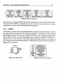
xiv
^NV
Ml I I '
'
,
Depuração
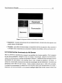
Processador
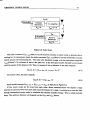
Sensores
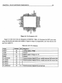
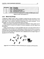
Figura 2; Diagrama de Blocos do Protótipo do Nó Sensor.
• Expansível - O projeto de hardware deve ser expansível pois o nó sensor deve dar suporte a um
grande número de aplicações.
• Tamanho - para efeito de demonstração, os dispositivos devem ser pequenos. Mas, tamanho é
a restrição menos importante pois este projeto é apenas um protótipo e não um nó sensor real.
2.2 Componentes funcionais do Nó Sensor
Figura 2 apresenta a arquitetura de sistema de um protótipo de nó sensor genérico. Ele é composto
de seis blocos principais: unidade de fonte de energia, comunicação, unidade de processamento,
unidade de armazenamento, interface de depuração e sensores. A unidade de fonte de energia consiste
normalmente de uma bateria e um conversor dc-dc e tem a função de alimentar o nó sensor. A
unidade de comunicação consiste de um canal de comunicação sem fio bidirecional. A maioria das
plataformas usam rádio de curto alcance. Outras soluções incluem laser e mídia infra-vermelho.
A unidade de processamento é composta de uma memória interna para armazenamento de dados e
programas, um microcontrolador e um conversor analógico-digital para receber sinais do bloco dos
Breve Resumo em Português
XV
sensores. A unidade de armazenamento é uma memória externa que serve como memória secundária,
por exemplo, manter um "log" de dados. A interface de depuração é usada para programar e testar os
nós sensores. Este bloco pode ser omitido no produto final de nó sensor. A unidade de processamento
é um bloco que liga um nó sensor ao mundo físico e tem um grupo de sensores e atuadores que
dependem da aplicação da RSSF.
3 Componentes de Hardware
Nesta seção serão discutidos as escolhas dos componentes de hardware.
3.1 Unidade de Processamento
o microcontrolador usado neste projeto é o MSP430F169, fabricado pela Texas Instruments. Ele
tem baixíssimo consumo de energia, CPU de 16 bits e desempenho de 8 MIPS. Ele tem óOKbytes de
memória de programa e 2Kbytes de memória de dados. Ele possui uma interface de depuração padrão
JTAG, e também possui um grande número de ferramentas de desenvolvimento.
O MSP430 consome menos que 400 mA no modo ativo, operando em 1 MHz com 3V e pode
acordar de um estado de repouso em menos de 6 /is. Ele é ideal para permitir o nó sensor dormir e
acordar apenas quando necessário para processar alguma coisa.
O processador inclui um rico conjunto de periféricos como conversor analógico-digital, comunicação
serial, comparadores e temporizadores.
3.2 Memória Externa
Muitos algoritmos e aplicações requerem um grande número de dados para serem armazenados. A
quantidade de RAM no microcontrolador é limitada. A solução é adicionar uma memória externa que
funcionará como memória secundária.
O M25P40 [60] da ST é uma memória serial flash de 4 Mbit que é rápida e pode mudar para o
modo de operação de baixo consumo quando não for utilizada. Ela gasta 1,5ms para escrever a página
(256 bytes) e no modo de baixo consumo gasta 10/iW.
Breve Resumo em Português
xvi
3.3 Comunicação
A função de comunicação entre os nós sensores é realizada pelo CClOOO [16] fabricado pela Chipcon.
O CClOOO é um transceptor de baixo consumo, CMOS, qualificado para transmissão de dados de até
76,8 Kbit/s. No modo de baixo consumo, a corrente do CClOOO é 0,2 /xA. O CClOOO é projetado para
modulação FSK na banda ISM. BEAN é configurado para trabalhar na faixa de 915 MHz. É possível
controlar a potência do sinal de saída e portanto especificar qual o alcance do rádio, economizando
energia e diminuindo interferência. O transceptor também pode medir a intensidade do sinal de
recepção (RSSI), fornecendo uma idéia de quão distantes os nós sensores estão entre si.
Para permitir o estudo e desenvolvimento de outros rádios, foi definido um barramento de rádio
para o BEAN, no qual contem dez pinos. Usando o barramento de rádio, é possível modificar o
projeto do canal de rádio sem alterai* BEAN.
3.4 Barramento de Sensores
E desejável que o protótipo do nó sensor seja fácil de expandir para permitir uma variedade de
aplicações. A solução encontrada é definir um barramento de sensores. O barramento de expansão
provê uma interface de usuário para placa de sensores adicionais. Portanto, para servir em uma
aplicação específica, basta construir uma placa de sensores específica e conectá-la ao bai-ramento de
sensores do BEAN. Por exemplo, para uma estação metereológica, uma placa com os sensores de
temperatura, luz e humidade.
3.5 Depuração
Para depurar, quatro LEDS são adicionados ao projeto do protótipo. O consumo de corrente dos
LEDS pode ser maior que o do rádio, e portanto é aconselhável usá-los apenas para depuração. A
interface JTAG (lEEEl 149.1) é usada para programar e depurar o microcontrolador servindo também
para programar a memória flash.
3.6 Fonte de Energia
Como o projeto visa a construção de um protótipo, a opção foi usar uma fonte de alimentação pai'a
alimentá-lo.
Breve Resumo em Português
xvii
Um diferencial do projeto do BEAN é a possibilidade de medir o consumo de energia de cada
componente em particular (rádio, microcontrolador, barramento de sensores, memória externa e todos). Foi adicionado um resistor "shunt" na fonte de alimentação de cada componente, permitindo
medir o consumo de energia. Para o nosso conhecimento, este é o primeiro protótipo de nó sensor
com esta vantagem.
Outra opção interessante é conectar o barramento de sensores do BEAN com os pontos de medição
de outro BEAN. Isto levará a uma nova metodologia para avaliar dinamicamente o consumo de energia de algoritmos de RSSF e como a ação de medir será feita por outro BEAN, a medida será independente e não distorcida pelo ato de medir.
3.7 Outros componentes
E desejável saber quando um evento ocorre, como por exemplo, ao gravar a leitura do sinal de um
sensor. Adicionando um relógio de tempo real permite o nó sensor medir o tempo ou criar um livro
de "log". Também é possível criar um relógio de tempo real com o microcontrolador, mas também
é desejável colocar o microcontrolador em baixo consumo de energia para economizar energia. Esta
solução também faria o software mais complexo. A abordagem mais simples é adicionai- um componente de hardware.
É desejável que cada nó sensor tenha um identificador único como um número. Uma solução em
software é escrever um número no componente de memória na fase de programação. Embora isto
seja uma solução, uma solução via hardware é mais elegante.
O componente DS2417 [27] oferece uma solução simples para armazenamento e recuperação da
informação de tempo com um hardware mínimo. Este componente contem uma identificador único e
um relógio de tempo real implementado como um contador binário. Ele usa o protocolo 1-Wire onde
apenas um pino é necessário para alimentar e comunicar com este dispositivo.
4 Componentes de Software
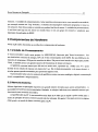
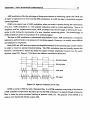
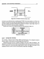
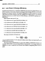
o projeto do BEAN também inclui o desenvolvimento de componentes de software. BEANj\PI é
composto de uma API (application programming interface) e os componentes que a implementam. A
API é um conjunto de funcionalidades para controlar, configurar e prover serviços dos componentes
Breve Resumo em Português
xviii
API
ADC
Driver
Timer
Driver
MCU
Config
Radio Driver
Memory
Led
Driver CClOOO Queue
Confíg
Driver
Digital
Clock
Power
I/O Sensor
Analog/Digital Timer
1-Wire
Software
SPIConfiguration
MCU
L
E
D
Memory
Radio
RTC
Serial
ID
Hardware
Figura 3: API.
do hardware através de uma interface bem definida.
A Figura 3 mostra a BEAN_API. Ela é composta de drivers que controlam o hardware e provê um
conjunto de funcionalidades para a camada acima. Embora temporizadores, conversores analógicodigital (ADC), pinos de entrada e saída sejam unidades periféricas do microcontrolador, eles estão
separados na figura para melhor explicar a integração hardware/software. Embora todos os componentes de software atuem dentro do MCU, a figura tenta explicar qual driver de software controla os
componentes de hardware. O hardware do relógio e o número serial comunicam com o MCU através
do protocolo de software 1-Wire. A memória externa e o rádio comunicam com o MCU através do
módulo SPI. Temporizadores são configurados usando o Digital Clock e Timer Driver. Para medir o
consumo de energia e os sinais dos sensores, é necessário usar o ADC, que é controlado pelo ADC
Driver.
A API comunica com a camada de cima que é um sistema operacional sendo desenvolvido pai-a o
BEAN. Alguns componentes de software são:
• MCU Config - O bloco de configuração do MCU permite mudar o modo de operação do MCU.
O MCU tem seis diferentes modos de operação e são capazes de tratar eventos de inteiTupção
• ADC Driver - A funcionalidade do ADC driver é configurar e manipular o módulo de hardware
ADC. O driver é usado para medir entradas analógicas e providas pelos sensores ou nível de
tensão.
• l-Wire - O módulo 1-Wire implementa o protocolo 1-Wire. Ele é usado para comunicar com o
componente DS2417.
Breve Resumo em Português
xix
• Digital Clock - Este módulo configura o relógio do MCU, provendo uma maneira de configurar
o relógio interno como múltiplos do relógio básico de 32 KHz.
• SPI Driver - O módulo de SPI configura o hardware SPI. Este protocolo é usado pela memória
externa e rádio.
• Memory Driver - O driver de memória controla a memória externa M25P40.
• Radio Driver - Este driver configura as propriedades do rádio como potência de saída, freqüência,
e também controla a transmissão e recepção de pacotes. Este driver define duas filas, uma para
o buffer de transmissão e uma para o buffer de recepção.
5 Questões Energéticas
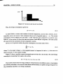
Nesta seção, um modelo de energia para nó sensores é apresentado. Valores são baseados em datasheets dos fabricantes. BEAN normalmente estará em um dos estados a seguir:
• Modo Down - tudo está desligado e o MCU está no modo de operação LPM3. A corrente é
10,5/iA e a potência é 31,5/iW.
• Modo de Recepção - o MCU está no modo ativo, o rádio no modo de recepção e o resto está
desligado. A corrente é de lOmA e a potência é de 30mW.
• Modo de Transmissão - o MCU está no modo ativo, o rádio está no modo de transmissão e o
resto está desligado. A corrente é 16,9mA e a potência é 51mW.
• Lendo a memória - o MCU está no modo ativo, a memória no modo de leitura e o resto
desligado. A corrente é 4,4mA e a potência é 13,2mW.
• Escrita na memória - o MCU está no modo ativo, a memória está no modo de escrita e o resto
está desligado. A corrente máxima é 15,4mA e a potência é 46,2mW.
• Modo de Sensoriar - o MCU está no modo ativo, o sensor específico está ligado e o resto
desligado. Este modo é dependente de qual placa de sensores está sendo usada.
Breve Resumo em Português
Microcontrolador (1,8-3,6) V
Down:0,l/^A
Atoa: 1,3 fj,A
Rádio (2.1- 3,6) V
Down:0,2uA Transmitir: 16,5mA
Memória (2,7-3,6)V
Down:10^A
Standby :50^
Relógio de Tempo Real (2,5-5,5)V
0,20Q/^A
Ativo: 400;üA
Receber:9,6mA
Ler:4mA
Escrever: 15mA
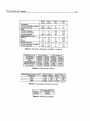
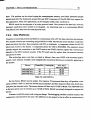
Tabela 1: Orçamento energético do BEAN.
Tabela 1 mostra o consumo de corrente e tensão da maioria dos componentes do BEAN.
Apenas para comparação, o BTnode [52] gasta 50mW no modo down e 450mW no modo de
comunicação. Claramente, BEAN é mais econômico.
Para comparar a plataforma, duas aplicações serão definidas. No primeiro cenário, o nó sensor
irá coletar e transmitir dados dos sensores e repassar dados recebidos. Este cenário opera em 1% do
tempo (MCU está no modo ativo). Neste período, lê a entrada do sensor, tenta receber pacotes | do
período e transmite em | do período. Ele nunca usa memória externa.
Para o segundo cenário, o nó sensor atua como repetidor, mantendo um log de eventos. Ele opera
em 1% do tempo. Neste período, recebe pacotes em | do período e transmite em l do período.
Escreve na memória externa usando | do período e também lê a memória externa | do tempo para
armazenar os pacotes recebidos e manter consistência dos dados. Os sensores não são utilizados.
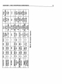
Tabela 2 mostra o consumo de corrente das plataformas BEAN e Mica2 e os ciclos do cenários.
Assume-se o mesmo consumo de corrente na placa de sensores para as duas plataformas.
Tabela 3 mostra os consumos de energia por componentes em mA-hora calculado para os dois
cenários para cada plataforma. O processador BEAN é mais econômico que o processador Mica2.
Tabela 4 mostra o tempo de vida (em número de meses) para cada cenário e plataforma, dependendo do tipo de capacidade da bateria. No cenário 1, usando uma bateria de 300mA-hr, BEAN pode
coletar dados por quase 26 meses.
Tabela 5 mostra quantitativamente a economia de BEAN comparado com Mica2 nos dois cenários.
BEAN pode consumir quase que 50% a menos que Mica2. A economia principal é do processador e
memória externa do BEAN.
Breve Resumo em Português
xxi
Processador
corrente (operação completa)
corrente dormindo
Rádio
corrente recebendo
corrente transmitindo
corrente dormindo
Logger Memória (max)
Escrever
Ler
Dormir
Placa de Sensores
con-ente (operação completa)
corrente dormindo
BEAN
(mA)
Mica2
(mA)
Cenário 1
(%)
Cenário 2
(%)
0,4
0,0013
8
0,008
1
99
1
99
8
12
0,002
8
12
0,002
0,75
0,25
99
0,75
0,25
99
15
4
0,01
35
10
0,02
0
0
100
0,25
0,25
99,5
5
0,005
5
0,005
1
99
0
100
Tabela 2: Orçamento Energético do BEAN e do Mica2.
Calculado mA-hr
Plataforma
Processador
Rádio
Logger Memória
Placa de Sensores
Total (mA-hr)
Ciclo Cenário 1
BEAN
Mica2
0,00529 0,08792
0,09198 0,09198
0,01
0,02
0,05495 0,05495
0,16222 0,25485
Ciclo Cenário 2
BEAN
Mica2
0,00529 0,08792
0,09198 0,09198
0,05745 0,1324
0,005
0,005
0,15972 0,3173
Tabela 3: Consumo em mA-hora.
Capacidade da bateria (mA-hr)
Plataforma
250
1000
3000
Ciclo Cenário 1
BEAN Mica2
2,14
1,36
8,56
5,45
25,69
16,35
Ciclo Cenário 2
BEAN Mica2
2,17
1,09
8,7
4,38
26,09
13,13
Tabela 4: Capacidade da bateria em meses.
I
Cenário 1
Cenário 2
Economia de BEAN
36,35%
49,66%
Tabela 5; Economia de BEAN.
Breve Resumo em Português
xxii
6 Conclusão
Uma plataforma computacional foi projetada, chamada BEAN, que inclui componentes de software
e hardware, usada como protótipo de um nó sensor. Ele permite testar e demonstrar algoritmos para
RSSF. Este sistema embutido é capaz de realizar todas as tarefas que um nó sensor real deve realizaie também tem as mesmas características como restrições de energia, memória e processamento.
BEAN pode consumir quase que 50% menos que o atual estado-da-arte Mica2 Mote. BEAN é
eficiente na questão de energia porque a MCU do BEAN é um dos microcontroladores mais eficientes
em termos de energia que existe atualmente, gastando cerca de 0,361 nJ por instrução. Além de
energia, outras vantagens do BEAN são preço e a não necessidade de um dispositivo dedicado.
BEAN é genérico porque ele possui um barramento bem definido, sendo capaz de um grande
número de aplicações. É necessário apenas uma placa de sensores específica para a aplicação. BEAN
também suporta o estudo de outros tipos de rádio porque BEAN tem um barramento de rádio bem
definido.
Este projeto também inclui o desenvolvimento de componentes de software, a BEAN_API. Um
modelo básico de energia para nó sensor e o orçamento energético do BEAN também são discutidos.
Chapter 1
Introduction
[The Universe] is written in mathematical language.
Galileo Galilei
Wireless sensor network (WSN) is composed of hundreds or thousands of autonomous and compact devices called sensor nodes. The objective of this network is to collect data. The availability of
integrated low-power sensing devices, embedded processors, wireless communication kits, and power
equipment are enabling the design of sensor nodes. Figure 1.1 illustrates a WSN. Each dot represents
a sensor node. Each device senses the environment, processes and usually transmits the data to an
external observer called base station.
Wireless Sensor Network has the potential for many applications and some already exists, for example in a large metropolis to monitor traffic density and road conditions; in engineering to monitor
bridges [50] and buildings structures; in a forest for fire detection [81] , in other environments like
oceans and air resources, in precision agriculture; in disaster recovery service; in condition based
maintenance devices like powerplants; in biomedicine [83]; in a smart kindergarten to create a development problem-saving environment for early childhood education [55]. Other applications include
managing complex physical systems like airplane wings and complex ecosystems.
A sensor node is composed of a power unit, processing unit, sensing unit, and communication
unit. The power unit has the purpose to power the node. The processing unit is responsible to collect
and process signals captured from sensors and transmit them to the network. Sensors devices are
devices that produce a measurable response to a change in a physical condition like temperature and
pressure. The wireless communication channel provides a medium to transfer signals from sensors to
1
CHAPTER 1. INTRODUCTION
2
Figure 1.1; Wireless sensor network.
exterior world or.a computer network, and also an internal mechanism of communication to establish
and maintain of WSN.
Power consumption is and will be the primary metric to design a sensor node. While there is the
Moore's Law that predicts doubling the complexity of microelectronic chips every 18-month [68],
and Gilder's Law [68], which theorizes a similar exponential growth in communication bandwidth,
there is no equivalent forecast for battery technology.
1.1
WSN Architecture
This section gives an overview of the WSN architecture. WSNs are networks composed of a large
number of sensor nodes. The objective of these networks is to collect data. Sensor nodes are usually deployed over a desire area, then they wake-up, self-test and establish dynamic communications
among them, composing a network [80].
WSNs usually do not have an infrastructure, like cellular phone or local wireless networks. WSN
is considered as a special type of ad hoc network, since its topology is dynamic, due to the fact
that sensor nodes can wake-up joining the network, or go to sleep, leaving the WSN. An important
characteristic is that the flow of data is typically unidirectional. The information flows from source
nodes to one or more access points.
Sensor nodes do generic tasks such as computing, transmitting data and monitoring using specific
sensors.
CHAPTER 1. INTRODUCTION
3
The key resource of a WSN is the stored energy. Each sensor node is composed of a small battery,
with a limit capacity. It is almost infeasible to recharge all battery since WSN can be composed
of thousands of sensor nodes. Therefore, the WSN project focus, from hardware design to network
protocols, is saving energy. Other sensor node restrictions include memory and processing power.
A WSN tends to be application-dependent, in other words, the hardware and software requirements and the operation modes vary according to the application.
1.2
Embedded System
Embedded system, as defined in [7], is a combination of computer hardware and software, and perhaps additional mechanical or other parts, designed to perform a specific function. They are present in
equipmeni^i-such as electric coffee machines, cameras and cellular phones. Opposite to personal computers that are capable of executing innumerous tasks, they are designed for specific functionalities,
such as controlling the sparks in a car engine or controlling a microwave oven. Using microcontrollers
and microprocessors for these tasks allows automation of manual tasks. Many microcontrollers have
been developed for specific applications in a way to aggregate a set of small functionalities. For example, advanced mathematical functions do not need to be present in a coffee machine microcontroller.
The small cost of these devices allows their uses at a great number of equipments.
Embedded systems compromise cost with functionalities. In this way, a minimal hardware and
software should be utilized to attend system requirements and minimize cost.
Sensor nodes can be seen as a special case of embedded systems and benefit from the large body
of knowledge already present.
1.3
Objective and Motivation
The objective of this work is to design an embedded system, that includes software and hardware
components, which will be a testbed prototype device for wireless sensor networks. This sensor node
prototype is called Brazilian Energy-Efficient Architectural Node (BEAN).
In this document, the design considerations and component choices for a testbed prototype device
for WSN will be discussed. We present the state-of-the-art for sensor node architectures, investigating
and analyzing some of the architectural challenges posed by these devices, including a survey of
CHAPTER 1. INTRODUCTION
4
sensor node platforms and energy management techniques. WSN can be seen as a special case of
embedded system and benefit from the large body of knowledge already present. A comparative
study of component-off-the-shelf (COTS) such as microcontrollers, battery types, and radio devices,
which are very important for system design, is presented. The design focus on individual components
and not in subsystem level details. Hardware choices will be discussed, as well as software solutions.
Software components that act as "device drivers" are presented in this work. We also define and
present an application programming interface (API) that can be used in other projects.
To our knowledge, BEAN is the first sensor node that allows measuring the power consumption of
each component. BEAN is also one of the most recent design that uses the newest Texas Instruments
MSP430F169 microcontroller. Finally, BEAN is the first sensor node prototype designed in Brazil.
The major motivations for this work are the necessity of a sensor node prototype for the SENSORi^T project [85] and also that there is no computational platform for wireless sensor network
in the Brazilian national market since it is a recent research topic. Finally, it is very important the
development of this technology, having the complete knowledge from the hardware to the software.
As stated by NSF [66] WSN is one of the greatest networking research challenges present nowadays.
1.4
Text Organization
"^This work is organized in seven chapters. Chapter 2 discusses related work for sensor node platforms
depicting platforms, components, operating systems and their contributions.
Chapter 3 presents the system architecture of a generic sensor node prototype pointing to BEAN
architecture.
Chapter 4 comments about hardware components used by BEAN. A comparative study of COTS
such as microcontrollers, battery types, and radio devices for system design, is presented. This chapter
also discuss the project decisions for BEAN.
Chapter 5 discusses the software components, called BEAN_API. It includes a set of "device
drivers" to control and configure the hardware components.
Chapter 6 discusses energy issues, presenting a basic version of an energy model for a sensor node.
We discuss the difference between power and energy, between low-power and energy efficiency, and
two power saving schemes. We also discuss the minimum required time for the memory device to go
to the power down mode saving energy. Finally, the power budget of BEAN is presented.
CHAPTER 1. INTRODUCTION
Chapter 7 presents the conclusions and new ideas for future works.
Chapter 2
Related Work
Intellectuals solve problems, geniuses prevent them.
Albert Einstein
This section surveys the current state-of-the-art for sensor node platforms depicting platforms,
components, and operating systems (Table 2.1 [99]). The majority of the components will be analyzed
in this work. Most of the related work uses battery as power supply unless otherwise specified.
At Berkeley, the Smart Dust project [49] aims at developing sensor nodes of millimetric size.
Their focus is on miniaturization of sensor nodes so that it has the size of a dust particle. Since this is
a long term project, the first step was the development of the Mote's family. WeC Mote (Figure 2.6)
and CCR mote were the first two types of sensor node developed in this project. CCR mote used
laser as communication media and WeC Mote used radio. The laser communication presented some
problems that will be discussed in section 4.3. Berkeley project opted to use radio devices. Then, they
developed Rene, Mica Mote (Figure 2.3) and finally to Mica2 Mote (Figure 2.4). The designer claims
that the advantage of the latter is its more robust radio. Another advantage is that it does not need
a co-processor to reprogram the sensor node since Mica microcontroller needs an extra processor
to help reprogram its memory. Mote family uses TinyOS [37], a compact, and simple event-based
operating system. Mica2Mote is one of the most commercialized sensor nodes [22].
One of the Mica2Mote advantage is the expansion bus that allows the connection of devices called
sensor boards. Separating the sensor boards from the radio and microcontroller allows the Mica2Mote
to be generic and capable of a variety of applications. The Mica Weather Board, stacked to the processor board via the 51 pin extension connector, includes temperature, photoresistor, barometer, humidity
6
CHAPTER 2. RELATED WORK
7
and thermopile sensors. Other advantage of Mote's family is that it uses a hardware component to
generate an unique identifier number.
Mica2Dot (Figure 2.4) is a small version of Mica2 with all Mica2 capabilities except for the
voltage regulator and the expansion board, which has only 18 pins. Many sensor boards are available
such as magnetometer board, battery adapter, sounder ranging board and ultrasound ranging board.
Telos [92] (Figure 2.7) is the next-generation Mote platform. It will use a different microcontroller
and Zigbee radio channel, which is an IEEE 802.15.4 radio, providing only 50 meter range. The radio
has an internal FIFO, allowing the ndcrocontroller to sleep while receiving a packet. A more complete
discussion on the radio device is presented at section 4.3. Telos has an optional external memory and
uses an USB component to connect to a PC.
For the gateway, the Mica's family has the MIB600CA, an Ethernet Interface Boai'd [22]. The
MIB600CA provides Ethernet (10/100 Base-T) connectivity to the MICA2 family of motes for communication and in-system programming. The MIB600CA allows remote access to sensor network
data via TCP/IP.
Berkeley project also constructed Spec Mode (Figure 2.13), a general-purpose sensor node that is
customized for miniaturization, achieving reduced size [38].
The PicoRadio project [73] at Berkeley Wireless Research Center is another project at Berkeley.
The objective is to develop a low-cost and low-power sensor node. Its focus is on the radio hardware,
link and network layer stack.
Medusa Mk-2 [14] (Figure 2.2) and iBadge [55] are sensor nodes from UCLA. These sensor
nodes use more than one processor and iBagde also include a Bluetooth chip. Mk-2 is also equipped
with a set of ultrasound transceivers that are used to perform high accuracy distance measurements
between adjacent nodes. iBadge includes a speech processing unit, a microphone, a localization unit,
an environment sensing unit with humidity, light, pressure, temperature sensors, and a orientation unit
composed of accelerometer and magnetic sensors. iBadge was used in a smart Kindergarten to create
a development problem-saving environment for early childhood education.
Generalized Network Of Miniature Environmental Sensor (GNOMES) is a project from Rice
University [105]. Its MCU is the MSP430F149 Texas Instruments. It has an accelerometer expansion
for structural analysis and GPS for coordinating sensors with location. It álso has a sensor bus that
allows for additional application specific sensor boards. The RS232 interface is used to communicate
with a computer. It can use Ethernet via its HOBBIT board. A communications header allows for
CHAPTER 2. RELATED WORK
7
and thermopile sensors. Other advantage of Mote's family is that it uses a hardware component to
generate an unique identifier number.
Mica2Dot (Figure 2.4) is a small version of Mica2 with all Mica2 capabilities except for the
voltage regulator and the expansion board, which has only 18 pins. Many sensor boards are available
such as magnetometer board, battery adapter, sounder ranging board and ultrasound ranging board.
Telos [92] (Figure 2.7) is the next-generation Mote platform. It will use a different microcontroller
and Zigbee radio channel, which is an IEEE 802.15.4 radio, providing only 50 meter range. The radio
has an internal FIFO, allowing the microcontroller to sleep while receiving a packet. A more complete
discussion on the radio device is presented at section 4.3. Telos has an optional external memory and
uses an USB component to connect to a PC.
For the gateway, the Mica's family has the MIB600CA, an Ethernet Interface Boai'd [22]. The
MIB600CA provides Ethernet (10/100 Base-T) connectivity to the MICA2 family of motes for communication and in-system programming. The MIB600CA allows remote access to sensor network
data via TCP/IP.
Berkeley project also constructed Spec Mode (Figure 2.13), a general-purpose sensor node that is
customized for miniaturization, achieving reduced size [38].
The PicoRadio project [73] at Berkeley Wireless Research Center is another project at Berkeley.
The objective is to develop a low-cost and low-power sensor node. Its focus is on the radio hardware,
link and network layer stack.
Medusa Mk-2 [14] (Figure 2.2) and iBadge [55] are sensor nodes from UCLA. These sensor
nodes use more than one processor and iBagde also include a Bluetooth chip. Mk-2 is also equipped
with a set of ultrasound transceivers that are used to perform high accuracy distance measurements
between adjacent nodes. iBadge includes a speech processing unit, a microphone, a localization unit,
an environment sensing unit with humidity, light, pressure, temperature sensors, and a orientation unit
composed of accelerometer and magnetic sensors. iBadge was used in a smart Kindergarten to create
a development problem-saving environment for early childhood education.
Generalized Network Of Miniature Environmental Sensor (GNOMES) is a project from Rice
University [105]. Its MCU is the MSP430F149 Texas Instruments. It has an accelerometer expansion
for structural analysis and GPS for coordinating sensors with location. It álso has a sensor bus that
allows for additional application specific sensor boards. The RS232 interface is used to communicate
with a computer. It can use Ethernet via its HOBBIT board. A communications header allows for
CHAPTER 2. RELATED WORK
8
variable communications boards and an expansion port for connection with additional boards. The
communication uses Bluetooth or 900 MHz radio. GNOMES are designed to be battery powered with
an alternative power source for recharging the batteries (750mAH NiMH cell) such as solar panels. It
also has an external Real Time Clock.
PushPin [12] (Figure 2.5) is a sensor node that is part of an MIT project. Pushpin's requirements
also meet the wireless sensor network needs. It uses a different approach for communication, using
an infrared link. Its operational system Bertha [53] is an interesting work since it fits in the 8051
microcontroller and its purpose is for distributed system. The power supply is via power bus.
Some sensor nodes have already been developed with GPS interface. Multimodal Networks of Insitu Sensors (MANTIS) sensor node, called Nymphs [67] (Figure 2.11), is claimed by their authors
to be the first sensor node that supports GPS [1]. Mantis is a project from the University of Colorado
that uses ATMEGA as the microcontroller. They are üeveloping their own operating system, called
MantisOS, which is a multi-threaded OS. They have a clear, well-defined and documented API.
BTnode (Figure 2.10) is a sensor node from the Smart-its project [52]. It uses a Bluetooth radio
and a bluetooth stack component for TinyOS have being developed for this project. Martin [52] shows
that the Bluetooth device is suggested for applications that are active over a limited time period, with
few unpredictable bursts of very heavy network traffic (taking advantage of the high throughput).
The European Research group, EYES [28], developed a prototype for low-end sensor node (Figure 2.1). The processor used in this prototype is the MSP430F149, produced by Texas Instruments.
The sensor node is also equipped with an auxiliary serial EEPROM memory of 8 Megabits used for
application and data storage. They are also developing an operating system for wireless sensor network, called Preemptive EYES Real Time Operating System (PeerOS) [65]. The project has also
the idea to connect specific sensor board to the sensor node, but their expansion bus is not available.
Since the radio do not have a great range, it has to add to the design an external amplifier. The sensor
node is progranunable using a RS232 interface.
The Embedded Sensor Board (ESB) (Figure 2.12) is the sensor node for the Scatterweb project [82].
It uses the MSP430 processor and the RFM TRIOOI [76] radio component. The sensor is also embedded in the board, thus, it is not possible to change the application. It has many sensors that includes
microphone, tilt/vibration, luminosity, temperature and infrared movement sensor. The actuators are
LEDs and a beeper. Besides the transceiver, it also has infrared sender and receiver, hence, ESB can
receive IR commands from standard remote controls. ESBs communicate via the serial port with a
CHAPTER 2. RELATED WORK
9
standard computer for application development. ESBs communicate with mobile phones via the serial
port to connect to a wide-area mobile phone networks. This enables remote configuration of ESBs
via short messages (SMS) as well as reception of sensor data on arbitrary mobile phones world-wide.
ESB has a battery compartment for three AAA batteries. It also has a voltage controller to stabilize
the input voltage to 3 V and an additional connector for a solar panel.
/iAMPS (micro-Adaptive Multi-Domain Power-Aware Sensors) project [63] (Figure 2.8) and
WINS [106] (Figure 2.9) from Rockwell Science Center chose low power StrongARM (SA-1100)
microprocessor for computation, uses an energy management technique. /zAMPS can program to
change dynamically the voltage supply and clock frequency of the SA-i 100 from 74 to 206 MHz and
i
0.85 to 1.44 V, respectively.
I
WINS enables data rates of 100 kbits per second over ranges in excess of 100 meters. At the
j
link layer, a Time Division Multiple Access (TDN5A) protocol has been implemented. The processor
runs at 133MHz with 150 MIPS. The processor consumes 300 mW, the radio consumes 600 mW in
transmit mode and 300 mW in receive mode, and the sensor transducers consumes 100 mW. The type
of sensors are seismic, acoustic, magnetometer and accelerometer.
The Jet Propuision Laboratory (JPL) [2] from California Institute of Technology is developing
a project called SensorWeb, supported by National Aeronautics and Space Administration (NASA).
The Sensor Web is an independent network of wireless, intra-communicating sensor nodes (called
sensor pods), deployed to monitor and explore a limitless range of environments.The engineering
objective is to test the Sensor Web in harsh environments, as for instance Antarctica [33].
PODS [8] is a research project in University of Hawaii that built WSN to investigate why endangered species of plants will grow in one area but not in neighboring areas. They deployed camouflaged
Í
sensors node, called Pods, in Hawaii Volcanos National Park. The Pods, consist of a computer, radio
•
transceiver and environmental sensors sometimes including a high resolution digital camera, relay
I
sensor data via wireless link back to the Internet. Bluetooth and IEEE 802. lib are chosen as channels
^
and data are delivered in IP packets. Two types of sensor data are collected, weather data and image
;
data.
i
Some commercial sensor nodes are already available. Millennial Net [61] builds heterogeneous
I
WSNs, dividing the networks in sensor nodes (endpoints), routers, and gateways. Its sensor node is
Í
called i-Bean, its typical range is 30m and data rate up to 250 kbps.
.
i
Ember [31] is another commercial solution. Its sensor node uses the Atmega 64L processor and
CHAPTER 2. RELATED WORK
10
CC1020 radio. It also has a temperature sensor and 2-Axis accelerometer.
MicroStrain [86] has launched one of the newest sensor node. It has a 8-bit microcontroller, Flash
EEPROM for sensor data logging, ADC of 16-bit resolution and a radio transceiver. But, the major
contribution is an energy-harvester. MicroStrain is developing an energy-harvesting scheme based
on storing cyclic strain energy by rectifying piezoelectric fiber output into a capacitor bank. When
the capacitor voltage reaches a preset threshold, power is transferred to an integrated wireless sensor
node [77].
The IEEE 802.15.4 [42] specification is a cost effective low data rate (< 250 kbps), 2.4 GHz and
868/928 MHz wireless technology designed for short range and personal area networking. Target
markets for the IEEE 802.15.4 Standard include industrial control and networking, home automation
and control, inventory management, human interface devices, as well as wireless sensor networks.
The IEEE 802.15.4 Standard is the bas?s of an application and network layer protocol known as
ZigBee [3]. The ZigBee Alliance is an association of companies working together to create software
inter-operability certification and testing for IEEE 802.15.4 systems.
The IEEE 802.15.4 Standard details the Physical Layer (PHY) and Medium Access Control
(MAC) specifications, and offers the building blocks for different types of networking. Key benefits of the IEEE 802.15.4 and ZigBee standards include extended battery life over current wireless
standards, mesh and star network topologies, and cost effectiveness.
Range for ZigBee products is expected to be 30 meters in typical homes, compared to iO meters
for Bluetooth products (without additional power amplifier) [3].
CHAPTER 2. RELATED WORK
11
Sensor Node
Radio
Processor
Operating system
Memory
BTNode
Ericsson ROK
ATmegal28L
TinyOS
64KB
StrongARM
RedHat
512KB
SA-1100
and eCos
Flash
Connexant
StrongARM
AtC/OS-II
4MB
RDSSS9M
SA-1100
PicoNode
Proprietary
DW8051
N/A
N/A
PushPin
IrDA
■ Cygnal
Bertha
N/A
transceiver
C8051F016
MSP430F149
N/A
32KB
101007
/xAMPS
LMX3162
WINS
Flash
83F8851
GNOMES
Bluetooth or
900 MHz radio
Eyes
TOlOOl
MSP430F149
PeerOS
8 Mbit
WeC Mote
TRIOOO
AT90LS8535
N/A
32KB
Mica Mote
TRIOOO
ATMEGA 103L
TinyOS
512KB Rash
Mica2 Mote
CCIOOO
ATMEGA128L
TinyOS
4 Mbit Flash
Telos
CC2420
MSP430F149
TinyOS
4 Mbit Flash
Nymphs
CCIOOO
ATMEGA128L
MantisOS
64kB EEPROM
ESB
TRIOOI
MSP430F149
N/A
8kB EEPROM
Medusa
TRIOOO
ATMEGA128L
N/A
1 MB Flash
N/A
N/A
MK-2
AT91FR4081
ARM THUMB
IBadge
TRIOOO
AtMEGA 103L
Bluetooth
TMS320VC5416
ROK101007
'BEAN
'
CCIOOO ^
:
MSi^0F16^:|
YATOS[97}
Table 2.1: Sensor Node Platforms.
V
4Mbit
CHAPTER 2. RELATED WORK
Figure 2.3: Mica.
Figure 2.7: Telos.
12
Figure 2.4: Mica2 and Mica2-dot.
CHAPTER 2. RELATED WORK
13
N "■
. 'li a
Figure 2.9: WINS
Figure 2.10: BTnode.
7,
_»m «c:
'f '
■ - .n(iiii:iMr:;! f - .^'i
f-. .1' ^
>.
Figure 2.11: Nymph.
Figure 2.12: ESB.
Figure 2.13: Spec.
'V
Chapter 3
Sensor Node Architecture
Hardware is the part of a computer system that can be kicked and
software is the part that can only be screamed at.
-Unknown
In this section we discuss WSN components, some characteristics and requirements of a sensor
node prototype and present the system architecture of a generic sensor node prototype.
3.1
WSN Components
WSNs can be classified according to its organization as hierarchical (sensor nodes self-organized in
clusters) or flat; to its composition as homogeneous (the same type of sensor node) or heterogeneous
(different types); and to its mobility as static (immobile) or mobile [79].
In a WSN, the information flows from source nodes to one or more access points. An access
point can be a sensor node with the same or more hardware capability. The access point purpose is to
collect data fi-om the network and send to an external observer, called base station [54].
The project of a more computational powerful access point is outside the scope of this work. Our
project also does not include any mobile feature.
The task that sensor nodes must be able to do includes monitor their physical environmental,
process their measurement data and forward other sensor nodes readings.
14
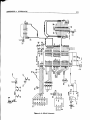
CHAPTER 3. SENSOR NODE ARCHITECTURE
15
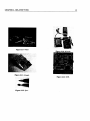
Debug
Processor
Sensors
Figure 3.1: Block Diagram of Sensor Node Prototype.
3.2
Sensor node functional components
Figure 3.1 presents the system architecture of a generic sensor node prototype. It is composed of
six major blocks: power supply, communication, processing unit, storage, debugging interface and
sensors. The power supply block has the purpose to power the node and usually consists of a battery
and a dc-dc converter. The communication block consists of a bi-directional wireless communication
channel. Most of the platforms use a short-range radio. Other solutions include laser and infrared
media. The processing unit is composed of internal memory to store data and applications programs,
a microcontroller to process data and an Analog-to-Digital Converter to receive signal from the sensing block. The storage unit is an external memory device that works as a secondary memory, keeping
a data log. The debugging interface is used to program and test the sensor node, for example, programming interface, LEDs, serial interface, JTAG (lEEEl 149.1). This block can be omitted in a final
sensor node product. The sensing unit block links the sensor node to the physical world and has a
group of sensors and actuators that depends on the application of the wireless sensor network.
CHAPTER 3. SENSOR NODE ARCHITECTURE
3.2.1
16
Processing Block
A very interesting questions is: should there be a dedicated processing element for each I/O device
or should the processing of the I/O devices be centralized? For example, besides the single CPU unit,
other approach is to use two general purpose processors: one handling the communication block and
one handling the other devices.
Sensor nodes may act as a router, forwarding packets meant for other nodes. Srivastava [75]
suggested the use of an intelligent radio hardware, with a dedicated CPU, that enables packets that
need to be forwarded to be identified and redirected from the communication block itself, allowing
the computing block to remain in Sleep mode, saving energy.
Since there is no such intelligent radio hardware COTS yet, it would need a processor in the
communication block to determine to forward or not the received packet. Thus, it would not save
a processor energy. This approach may be interesting if the main unit consumes much more energy
than the communication processor block.
BEAN approach is a single CPU handling multiple I/O devices. It is simpler and less expensive.
The communication block does not need a processor because BEAN has already the processing unit
to process the radio packets. This approach may change if the communication channel increases to a
very high rate and BEAN is overloaded and incapable of processing all the radio packets.
The processing unit may have other approaches such as finding the high-energy pieces of software
and move them to dedicated hardware. Lach [51] shows that implementing a JPEG compression
algorithm for WSN saves energy. This approach is interesting for a more robust or specific-application
sensor node, that is not BEAN purpose.
3.2.2
Sensing Blocic
Sensors can produce analog or digital signals. Analog sensors need an Analog-to-Digital Converter
(ADC). In general, microcontrollers have additional peripherals that include ADCs. Hence, initially,
sensor boards do not need dedicated ADCs. ADCs have a limited rate to converter signals, for example, the MSP430 family [44] is capable of 200.000 samples per seconds (ksps) divided in eight
channels. For complex sensor boards that need higher sample rates or larger channel number, a different approach is to embedded ADCs directly on the sensor boards.
Depending on the sensor type, it can change completely the sensor node design. For example.
CHAPTERS. SENSOR NODE ARCHITECTURE
17
an image sensor would need a very high bandwidth, which would require a communication block
redesign.
3.3
Characteristics and Requirements
This project does not intent to design a device that will be comparable to real-life wireless sensor
node. While in a real product size and cost are essential requirements, our design focus in a system
ease to expand with a number of sensors, robust and easy to reprogram.
Following is the design considerations, characteristics and requirements when designing BEAN:
• Energy-efficiency - Sensor nodes must be energy efficient. Sensor nodes have a limited amount
of energy that determines their lifetime. Since it is unfeasible to recharge thousands of nodes,
each node should be as energy efficient as possible. Hence, energy is the key resource, being
the primary metric for analysis. BEAN project focus on energy-efficient COTS.
• Power-Aware - The hardware should be able to estimate what energy is left, so algorithms can
adapt to the available power. BEAN is capable of measuring its own overall power consumption.
• Low-cost - It is desirable that sensor nodes be cheap since WSN may have hundreds or thousands of sensor nodes. For this purpose, BEAN uses only the necessary devices.
• Distributed sensing - Using a wireless sensor network, many more data can be collected compared to just one sensor. Even deploying a sensor with a large range, it could have obstructions.
Thus, distributed sensing provides robustness to environmental obstacles [32].
• Wireless communication - The sensor node needs to be wireless. In many applications, the environment being monitored does not have installed infrastructure for communications. Laying
wires may be too difficult or expensive, thus, sensor nodes should use wireless communication
channels. The data rate in WSN is low, thus, a short range transceiver in a license free band is
sufficient.
• Multi-hop - A sensor node may not reach the base station. The solution is to communicate
through multiple hops. Another advantage is that radio signal power is proportional to r^,
CHAPTER 3. SENSOR NODE ARCHITECTURE
18
where r is the distance of communication. Depending on radio parameters as shown in [56],
it can be more energy efficient to transmit many short-distance messages than one-long distance message. Thus, the sensor node should receive and transmit, needing a bi-directional
communication channel.
• Distributed processing - Each sensor node should be able to process local data, using filtering
and data fusion algorithms to collect data from environment and aggregate this data, transforming it to information. BEAN has a microcontroller for this purpose.
• Programmability - Since this component will be a test prototyping, it will be often reprogrammed for development of communication protocols and applications for WSN. Hence, the
progranmiing should be easy. BEAN chooses a microcontroller with embedded debug.
• Expandability - The hardware design must expandable with a number of sensors to support
a variety of applications. BEAN project defined a generic sensor bus and radio bus for future
expansion.
• Size - For demonstration purposes the devices should be reasonable small. But size is of less
important in our project since it does not need to be as small as a real-life wireless sensor nodes.
3.4
Challenges
Figure 3.2 illustrates some challenges for WSNs. Each block has its unique challenge. The storage
block was included in the processing unit and the debugging interface is not needed in a real-life
sensor node. A power management layer is required to control the main resource of a sensor node,
its energy level. The power management layer could use the knowledge of battery's voltage slope to
adapt dynamically the system performance [69]. Another advantage is that other energy source can
be added and the power management can make the best use of the energy resources. New network
protocols are necessary, including link, network, transport, and application layers to solve problems
like routing, addressing, clustering, synchronization and they have to be energy-efficient. A microkernel for sensor node is necessary. Many operating systems exist for small device (like handheld
and PDAs), but not so small as a sensor node and not aggressive on power management for long
CHAPTERS. SENSOR NODE ARCHITECTURE
19
Figure 3.2: System architecture and challenges of a sensor node.
life and wireless communication as well. Algorithms for filtering and data fusion are also necessary. Many other challenges exist, including localization of sensor nodes and security issues, such as
cryptography.
Although WSN is a recent research topic, many interesting works already exist such as microkernels [25], middlewares [102], scheduling algorithms [101], routing protocols [100], [46], deployment
algorithms [98] and architecture management scheme algorithms [80] for WSN.
Chapter 4
BEAN Hardware Components
But what.. is it good for?
Engineer at the Advanced Computing Systems
Division of IBM, 1968, commenting on the microchip
Make everything as simple as possible, but not simpler.
Albert Einstein
In this chapter, we will discuss the component choices for the hardware design of BEAN. A comparative study of COTS for the major sensor node prototype architectural block (processing, power,
communication, sensing, storage and debugging interface units) is presented. Then, we comment
about interfacing the radio with the MCU. Finally, we summarize the major BEAN hardware project
decisions.
4.1
Processing Unit
Since the sensor node is expected to communicate, process and gather sensor data, sensor nodes must
have processing units. The central processing unit of a sensor node determines to a large degree both
the energy consumption as well as the computational capabilities of a sensor node. Many different
types of CPUs can be integrated into a sensor node and they are discussed in this work. There are a
large number of commercially available microcontrollers, microprocessors and field-programmable
gate arrays (FPGAs), which allows a big flexibility for CPU implementations.
20
CHAPTER 4. BEAN HARDWARE COMPONENTS
4.1.1
21
Programmabie Logic
Many types of programmable logic are available. Complex Programmable Logic Devices (CPLDs)
consist of multiple PAL-like (Programmable Array Logic) logic blocks interconnected together via
a programmable switch matrix [6]. CPLDs are used for high-performance control-logic or complex
finite state machines but limited to the size of a few thousand gates. Although there is low-power
CPLDs, such as CoolRunner-H [107], that consumes as low as 14/xA standby current, their consumption is not as low as a sensor node should be. For example, CoolRunner-II operating at 1.8V and
20MHz, needs a current supply of 17.22 mA. WSNs are dependable on the application scenario. The
architecture of CPLD is not very flexible, being applicable for small application and is not capable of
implementing a CPU. For a specific application which needs a complex controller, CPLD may be an
option.
An Field Programmable Gate Array (FPGA) consists of an array of logic blocks, surrounded by
programmable I/O blocks, and connected with programmable interconnect [6]. FPGAs offer narrower
logic resources than CPLDs but offer a higher ratio of flip-flops [11]. Because of all the extra flipflops, reaching millions of gates, the architecture of an FPGA is much more flexible than that of a
CPLD [11]. Nowadays, FPGA presents some major disadvantages. First, their consumption is not
as low as a sensor node should be. Another disadvantage is that today is not possible to turn off
separate blocks of FPGAs. In addition to consuming more power, the FPGAs are not compatible with
traditional programming methodologies (i.e., no C compiler). It does not mean that FPGAs are not a
good solution for the near future. Maybe with the development of ultra-low power FPGAs, FPGAs
will be a good solution for sensor node monitoring a planet, since they have the advantage of being
reprogrammable and reconflgurable, eliminating the deployment cost in space applications.
In terms of energy, microcontrollers are a better solution than FPGAs. Microcontrollers may be
designed to be optimal and it is possible to turn their functional blocks off. In addition, FPGAs are
not capable of tuming off separate blocks. Even with this feature, turning off a FPGA block does not
mean turn off a functional block because it will depend on the partitioning algorithm. Finally, since
a FPGA block must be generic to implement any logical module, it will not be power optimized as a
microcontroller.
CHAPTER 4. BEAN HARDWARE COMPONENTS
4.1.2
22
Microcontrollers
A microcontroller is very similar to a microprocessor. The main difference is that a microcontroller
is designed specifically for use in embedded systems [7]. In general, microcontrollers are microprocessor with additional peripheral or support devices [5]. Microcontroller includes not only memory
and processor, but also non-volatile memory and interfaces such as ADCs, UART, SPI, counters and
timers. In this way, it can iterate with sensors and communication devices such as short-range radio
to compose a sensor node.
Some of the advantages of the microcontroller's higher level of integration as stated in [5] are:
• Lower cost - one part replaces many parts.
• More reliable - fewer packages, fewer interconnections.
• Faster - signals can stay on the chip.
Nowadays, there are many types of microcontrollers, ranging from 4 to 32 bits, varying the number
of timers, bits of ADC, power consumption, size of memory, etc. A discussion of these devices is
presented below.
Table 4.1 shows comparison of actual microcontrollers. Microcontroller Control Units (MCUs)
have many attributes like number of bits, flash memory, size of memory, number of ADC and timers,
operating voltage, current consumption and power modes. An important feature is the start-up time,
Since the MCU will usually go to idle mode, but It is not very often divulged.
The EM6603 [30], which is 4-bit, is ultra-low-power MCU but its computational power is also
very limited. It is used for Radio Frequency Identification (RFID) applications. The advantages
of Motorola DragonBall MC9328MX1 are that it is 16-bit and has a Bluetooth Accelerator radio
interface. It also has a Time Processing Unit (TPU), a co-processor unit that seems to be able to
perform various real-time control tasks (like sampling a pin). The shortcomings are performance
(only 2.7 MIPS), no integrated memory or flash, relatively large footprint (100 or 144 pins), not
ultra-low-power.
The ARM family has floating-point computational capabilities, being a possibility for devices
demanding more computational power, such as a gateway or a robust sensor node, which can be
the head of hierarchical wireless sensor network cluster. One common example is the processor
module Intel StrongArm SAllOO embedded controller. The SAllOO is a general-purpose, 32-bit
CHAPTERS BEAN HARDWARE COMPONENTS
23
RISC microprocessor based on the ARM architecture that is rated as the most efficient processor (in
MIPSAVátt). The processor offers a 16KB instruction cache, a 8KB data cache, serial I/O and JTAG
interface all combined in a single chip. Program and data storage are provided by 1MB SRAM and
4MB of bootable flash memory. Connection with the sensor modules is easily achieved using a 4-wire
SPI interface. The processor has three states: normal, idle and sleep that can be controlled to reduce
power consumption.
The choice of MCU depends on application scenario. The ideal choice of microcontroller is the
one that matches its performance level with application's need. Other factors that affects the selection
of the proper microcontroller besides energy level include word size, peripherals, memory, speed,
physical size, price, availability, personal experience, and vendor support.
CHAPTER 4. BEAN HARDWARE COMPONENTS
u
1
I
n
<
.a i
t
V
24
a
s|
I ^ OS
(S
60 u
M
I J
è
m
>
cn
^ ffi (§)
® 5
<
3.
®
cs
8
^ u
(£
i
iS <
3. E
«o VO
1i
JS
d
1
cn
VO
>
«n
«o
5
>
VOI
CS
rí
£
u
B
P
! S
^ :2
®
>
r~ «n
c4 «n
o
>
VO
cíI
CO
I
so
a
(S
i
••
X)
o o
m
I
PQ CQ
cs
«
2
i
o
£
oo 3
£
00
VO
i
i
<
Z
iS
03
oo 00
00
VO cs
cn
00
VO
u
• rt
«o
00
«D ri
00
cd
00
o
"S
CO
o
X
00
u
t
V)
o
U
X
00
VO
U
m •a a
§ s
^ fO
<§ S
CHAPTER 4. BEAN HARDWARE COMPONENTS
25
340
Opamtlng Mod**
Figure 4.1: Typical Current Consumption vs. Operation Modes [93J.
4.1.3
Texas Instruments MSP430
The microcontroller used in our project is the MSP430F169, produced by Texas Instruments. It is a
good option for sensor nodes since it is a 16-bit, 8 MIPS, providing more computational power than
8 bit microcontrollers, and also ultra-low power. It has 60kbytes of program memory and 2kbytcs
of data memory. It is equipped with a full set of analog and digital processors. It has embedded
debugging and in-system flash programming through a standard JTAG interface, and is supported by
a wide range of development tools including gcc [62] and lAR Embedded Workbench [41 ].
The MSP430 family has six different operating modes and is fully supported during interrupt
event handling. There are the active mode (AM) and five Low-Power Modes (LPMO, LPM1, LPM2,
LPM3 and LPMO, LPM4). An interrupt event awakes the system from each of the various operating
modes and returns, using the RETT instruction, to the mode that was selected before the interrupt
event occurred. The current consumption of each operation mode is shown in Figure 4.1. The microcontroller can be configured to consume only the energy necessary to its works through the selected
operation mode. More information can be found at [93].
The MSP430 is a RISC microcontroller that employs a von-Neumann architecture, therefore, all
programs and data share a single address space. The CPU has sixteen registers that provide reduced
instruction execution time. This reduces the register-to-register operation execution time to one cycle
of the processor frequency. Four of the registers are reserved for special use as program counter,
stack pointer, status register, and constant generator (Figure 4.2) [44]. The remaining registers arc
available as general-purpose registers. Peripherals are connected to the CPU using a data address and
control bus, using specific registers for control and data transfers sharing the memory space, and can
be handled with all memory manipulation instructions.
The MSP430 consumes less than 400 mA in active mode operating at 1 MHz in a typical 3V
CHAPTER 4. BEAN HARDWARE COMPONENTS
Figure 4.2: Register Overview [44J.
26
Figure 4.3; Low-Power CPU [44J.
system and can wake up from a 2mA standby mode to fully synchronized operation in less than 6 ^s.
These exceptionally low current requirements, combined with the fast wake-up time (6us), enable a
developer to build a system with minimum current consumption and maximum battery life.Figure 4.3
shows the current consumption of an application that switches between active and stand-by modes.
MSP430 family has a rich peripheral set. It has an abundant mix of peripherals and memory sizes
enabling true system-on-a-chip designs as illustrated in Figure 4.4 [44]. The peripherals include a
12-bit Analog-to-Digital converter, multiple timers (some with capture/compare registers and PWM
output capability), integrated precision comparator, on-chip clock generation, hardware multiplier,
CHAPTER 4. BEAN HARDWARE COMPONENTS
27
Figure 4.4: Functional block diagram of MSP430xxl6x [44].
USART(s), Watchdog Timer, General Port Input/Output, and multiple Input/Output with extensive
interrupt capability and others.
The Basic Clock Module of MSP430 is design for low power consumption applications. Applications should use low clock frequency for energy conservation and time keeping but it also should
use high clock frequency for fast reaction to events and fast burst processing.The faster it finishes the
processing, the more time at low-power mode it has.
The Basic Clock Module addresses the above conflicting requirements by allowing the designer
to select from the three available clock signals:
• ACLK (Auxiliary clock) - For optimal low-power performance, the ACLK can be configured
to oscillate with a low 32,786-Hz watch-crystal fi^uency, providing a stable time base for
the system and low power stand-by operation. ACLK is software selectable for individual
peripheral modules.
• MCLK(Main clock) - MCLK is used by the CPU and system. The MCLK can be configured
to operate from the on-chip digitally controlled oscillator (DCO) which is only activated when
requested by events.
• SMCLK (Sub-main clock) - The SMCLK can be configured to operate from either the watch-
CHAPTER 4. BEAN HAMDWARE COMPONENTS
28
Figure 4.5: Frequency versus Supply Voltage [44].
crystal or the DCO, depending on peripheral requirements. SMCLK is software selectable for
individual peripheral modules.
The clock distribution and divider system is provided to fine tune the individual clock requirements. All basic clock-module configurations are under software control.
The Basic Clock Module includes two or three clock sources:
• LFXTICLK - low-frequency/high-frequency clock source. One oscillator that can be used
with low-frequency watch crystals, standard crystals, resonators, or external clock sources.
• XT2CLK - high-frequency clock source. This optional high-frequency oscillator can also use
standard crystals, resonators, or external clock sources in the 450-kHz to 8-MHz range.
• DCOCLK clock source - The digitally controlled oscillator (DCO) is an integrated RC-type
oscillator in the Basic Clock Module. The DCO frequency can be tuned by software.
Using the DCO, it is possible to control the operating frequency. The operating frequency depends
on the supply voltage as show in Figure 4.5 [44]. The MCU operates between 1.8 and 3.6 V. To
program the MCU, the supply voltage should be above 2.7 V. We can model the graph using the line
equation. Let's y be the frequency (MHz) and x the supply voltage (V):
^(^) = ^*(a:-1.8)-K4.15
(4.1)
To operate at 3.3 V, the frequency should be 7.358Mhz. BEAN was designed to use the LFXTICLK
with a 32,768-Hz watch crystal and the DCO at 7.358Mhz.
CHAPTER 4. BEAN HARDWARE COMPONENTS
29
8113
ilSit
fCUUUULJLJUUUUUUUUUU
PM « tl «1 « M tt 17 M •f •4tt«IIN4t
DVcc J1
p«.yA3
n.vM i!
Pe.8/AS
P6.8/A6/CMC0 i:
Pe.7/A7/0AC1/8V8JN
Vrv* i;
XM )•
XOUT/TOK )•
V||EF-/Vinp. 1"
P1.(Vti^CU( tt
P1.1/W0 11
PI .«mi u
pi.anMDii
P1.4/8MCU( J i«17 » Ji IP t1 IttSMIiMrMMMSIV
Figure 4.6; Pin Designation [45],
Figure 4.6 [45] shows the pin designation of MSP430. Table 4.2 illustrates the MCU port mapping, showing the port name, port number, if input or output or programable, and what function the
port was mapped to.
Table 4.2: MCU Port Mapping.
Name
Number
AVCC
64
Analog supply voltage
AVSS
62
Ground
DVCC
1
DVSS
63
Pl.O/TACLK
12
I
General-purpose digital I/O pin- enable interrupt IntO sensor bus
Pl.l/TAO
13
I
General-purpose digital I/O pin- enable interrupt Intl sensor bus
P1.2/rAl
14
P1.3/TA2
15
P1.4/SMCLK
16
0
General-purpose digital I/O pin Red Led
I/O
Mapped to
Digital supply voltage (3.3 V)
Ground
CHAPTER 4. BEAN HARDWARE COMPONENTS
30
Table 4.2: MCU Port Mapping.
Name
Number
I/O
P1.5AA0
17
0
General-purpose digital I/O pin Orange Led
P1.6/TA1
18
0
General-purpose digital I/O pin- Green Led
P1.7/TA2
19
0
General-purpose digital I/O pin- Yellow Led
P2.0/ACLK
20
P2.1/TAINCLK
21
I
General-purpose digital I/O pin RTC JNT- RealTimeClock
P2.2/CAOUT/TAO
22
I
General-purpose digital I/O pin PWMO
P2.3/CA0/TA1
23
I
General-purpose digital I/O pin PWMl
P2.4/CA1/TA2
24
I
General-purpose digital I/O pin- 1-Wire (Real Time Clock)
P2.5/ROSC
25
P2.6/ADC12CLK/
26
Mapped to
General-purpose digital I/O pin Dclk (Radio)
General-purpose digital I/O pin External Memory Hold
DMAEO
P2.7/TA0
27
General-purpose digital I/O pin - External Memory Write
P3.0/STE0
28
General-purpose digital I/O pin External Memory Chip Select
P3.1/SIMOO/SDA
29
SPI Mode External Memory
P3.2/SOMIO
30
SPI Mode External Memory
P3.3/UCLK0/SCL
31
SPI Mode External Memory
P3.4/UTXD0
32
o
UART mode (sensor bus)
P3.5/URXD0
33
I
UART mode (sensor bus)
P3.6/UTXD1
34
P3.7/URXD1
35
I/O
P4.0/TB0
36
I
General-purpose digital I/O pin (sensor bus)
P4.1/TB1
37
I
General-purpose digital I/O pin (sensor bus)
P4.2/TB2
38
I
General-purpose digital I/O pin (sensor bus)
P4.3/TB3
39
I
General-purpose digital I/O pin (sensor bus)
P4.4/rB4
40
I
General-purpose digital I/O pin (sensor bus)
P4.5/TB5
41
I
General-purpose digital I/O pin (sensor bus)
P4.6/TB6
42
I
General-purpose digital I/O pin (sensor bus)
General-purpose digital I/O pin -I2C (sensor bus)
General-purpose digital I/O pin -I2C (sensor bus)
CHAPTER 4. BEAN HARDWARE COMPONENTS
Table 4^: MCU Port Mapping.
Number
I/O
P4.7/TBCLK
43
I
General-purpose digital I/O pin (sensor bus)
P5.0/STE1
44
I
General-purpose digital I/O pin Chp.out (Radio)
P5.1/SIM01
45
0
SPI mode Dio (Radio)
P5.2/SOMI1
46
I
SPI mode Dio (Radio)
P5.3/UCLK1
47
o
SPI mode Dclk (Radio)
P5.4/MCLK
48
I/O
P5.5/SMCLK
49
General-purpose digital I/O pin Pclk (Radio)
P5.6/ACLK
50
General-purpose digital I/O pin Pdata (Radio)
P5.7/TBoutH/
51
Name
Mapped to
General-purpose digital I/O pin Pale (Radio)
SVSOUT
P6.0/A0
59
I
12-bit ADC - RSSI (Radio)
P6.1/A1
60
I
12-bit ADC - Sensor Bus
P6.2/A2
61
I
12-bit ADC - Sensor Bus
P6.3/A3
2
I
12-bit ADC - Sensor Bus
P6.4/A4
3
I
12-bit ADC - Sensor Bus
P6.5/A5
4
I
12-bit ADC - Sensor Bus
P6.6/A6/DAC0
5
I
12-bit ADC - Sensor Bus
P6.7/A7/DAC1/
6
I
12-bit ADC - Sensor Bus
RST/NMI
58
I
Reset input - jtag connector
TCK
57
I
Test clock - jtag connector
TDI
55
I
Test data input - jtag connector
TDO/TDI
54
I/O
TMS
56
I
VeREF
10
I/p
VREF
7
0
VREF-A^eREF-
11
0
SVSIN
Test data output port - jtag connector
Test mode select - jtag connector
31
CHAPTER 4. BEAN HARDWARE COMPONENTS
32
Table 4.2; MCU Port Mapping.
Name
Number
I/O
XIN
8
I
XOUT/TCLK
9
I/O
XT2IN
53
I
Input port for crystal oscillator XT2.
XT20UT
52
O
Output terminal of crystal oscillator XT2
4.2
Mapped to
Input port for crystal oscillator XT I.
Output terminal of crystal oscillator XTl
Power
The power supply block usually consists of a battery and a dc-dc converter and has the purpose to
power the node, since the sensor node needs energy to monitor the environment.
Since we are constructing a prototype, we opted to use an external power supply. A voltage
regulator could be added, whose purpose is to maintain the output voltage at a fixed value. Below, we
discuss some idea that can be used in future works.
It might be possible to extend lifetime of a sensor node by extracting energy from the environment,
for example light, vibration and RF. Amirtharajah et al. have demonstrated a MEMS system that
extracts electric energy from vibrations [4]. Nowadays, CMOS transistors and solar cell's arrays can
be co-fabricated. The Icarus process [40] combines solar cells, high voltage CMOS, and SOI (Siliconon-insulator)-MEMS structures on the same die. With the addition of isolation trenches, devices and
MEMS structures can be electrically isolated, and solar cells can be stacked to yield high voltages.
Table 4.3 [74] shows a comparison of energy sources based on a combination of published studies,
theory, and experiments.
Continuum Control Corp. [21] has launched the iPower enei^y harvesters. These devices, extract
electric energy from mechanical vibrations, motion, or impact, and store it for use by wireless sensors
or other electronic devices.
4.2.1
Batteries
Batteries supply energy to the sensor node. It is important to choose the battery type since it can
affect the design of a sensor node. Battery Protection Circuit to avoid the overcharge/overdischarge
CHAPTER 4. BEAN HARDWARE COMPONENTS
Energetic source
Solar (outdoors)
Solar (indoors)
Vibrations
Acoustic noise
Passive human-powered systems
Nuclear reaction
33
Power Density
15mW/cm^(direct sun)
0.15mW/cm^(cloudy day)
0.006mW/cm^(standard office desk)
0.57mW/cm^(< 60W desk lamp)
0,01-0,lmWW
3E-6mW/cm^a75dB
9,6-4mW/cm^ a lOOdB
l,8mW(shoe inserts)
SOmW/cm^ lE6mWh/cm^
Table 4.3: Comparison of energetic sources.
Battery
Alkaline-Mn02 (AA)
Silver Oxide
Li/Mn02
Zinc Air
Sealed Lead Acid
NiCd
NiMH
Li-ion
Li-Polymer
Rechargeable
No
No
No
No
Yes
Yes
Yes
Yes
Yes
Volumetric density(Wh/l)
347
500
550
1150
90
80-105
175
200
300-415
Environmental concerns
Yes
Yes
No
Yes
Table 4.4; Battery technology Comparison,
problem, power voltage regulator and other components may be added to the sensor nodes.
There are many types of batteries being available. Batteries can be divide into primary (nonrechargeable), and secondary (rechargeable). They can also be classified according to electrochemical
material used for electrode such as NiCd, NiZn, AgZn, NiMh, and Lithium-Ion.
Table 4.4, based on [68] and [34], compares most common batteries's types. NiMh and LithiumIon are the most commercialized rechaigeable batteries.
The battery type will depend on the application. If there is not a harvest energy source, nonrechargeable battery is a good choice since they have higher energy density. Among the rechargeable
batteries, Li-based batteries appear to be the best choice. However, there are a number of other considerations and the proper choice of battery technology is not obvious without a detailed examination
of the application operational profile. For instance, in a pulse-discharge scenario, a Li battery would
CHAPTER 4. BEAN HARDWARE COMPONENTS
34
perform poorly while a NiCd would perform well due to the lai:ge differences in the internal resistance
of these battery types. Furthermore, Li-based battery cost is higher.
Among the rechargeable battery types. Nickel Metal Hydride (NiMH) is the only environmentally
friend product. Its energy density is second only to Li-battery types and it can be recharged at any
time without experiencing voltage depression (memory effect). The disadvantage is that it needs
overcharge/overdischarge protection.
4.3
Communication
Sensor nodes must communication among them and also to a base station using a wireless communication channel. We explore three possibilities, laser, infrared and radio frequency (RF) channels.
4.3.1
Laser communication
The advantages of laser communications are:
• Spend less energy than radio over larger range.
• Security, since there is no broadcast and if a channel is intercepted it would interrupt the signal
• No need for antenna.
The disadvantages are:
• Needs line of sight ("LOS"), since the laser beam of the transmitting device must be lined up
to the receiver. It involves not only a temporal step but also a spatial acquisition step
• Sensible to atmospheric conditions.
• The communication is directional and due to the fact that sensor nodes will be deployed randomly, this is not an attractive solution.
The transmitting device uses a laser beam to send information and the receiver device uses a
photodiode or CCD array. Optical communication can be classified into two types, passive and active
communication. In active optical communication, the transmitting device generates its own laser
signal whereas in passive communication the laser signal is generated through a secondary source.
CHAPTER 4. BEAN HARDWARE COMPONENTS
35
Hollar [39] reports that the active laser consumes 50 mA. at 3V and could established communication
with distances up to 21.4 km. The passive cost of transmission is limited to the energy required to
deflect one of the mirrors, which in the case of the MEMS comer-cube-reflectors (CCRs) used in
COTS Dust amounts to 100 pJ/bit [39].
4.3.2
Infrared
Infrared communication is usually directional. Since sensor nodes will be deployed randomly, a good
solution adopted by PushPin project [12] is to use a diffiiscr made of siindblasted polycarbonate tubing
to create a more omni-directional communication range within a plane. But, the node still needs to be
aligning within a plane. PushPin project adopted the IrDA transceiver 83F8851 [91]. Its disadvantage
is a short-range of about Im. Its maximum current consumption in transmission mode is 10mA and
in receive mode is 25 mA. The advantage of infrared is no need for antenna.
4.3.3
Radio-frequency (RF)
RF communication is based on electromagnetic waves. One of the most important challenges in RF
communications devices is the antenna size. To optimize transmission and reception, an antenna
should be at least A/4, where A is the wavelength of the carrier frequency. Assuming a sensor node
with a quarter wavelength of 1 mm, the RF carrier frequency is 75 GHz, which is out of the range of
modem low power RF electronics. It is also necessary to reduce energy consumption with modulation,
filtering, demodulation, etc. RF communication advantages are its ease of use, integrality, and well
established in the commercial marketplace, which make it an ideal testing platform for sensor node.
Several aspects affect the power consumption of a radio including the type of modulation, data
rate, and transmission power. In general, radios can operate in three distinct modes of operation:
transmit, receive, idle. Most radios operating on idle mode results in high power consumption, almost
equal to receive mode, thus, it is important to shutdown the radio.
4.3.3.1
Modulation
Here, we discuss some popular modulation schemes, On/Off key (OOK), Amplitude Shift Key (ASK),
Frequency Shift Key (FSK), Gaussian Frequency Shift Key (GFSK) and Offset-Quadrature Phase
Shift Keying (0-QPSK).
CHAPTER 4. BEAN HARDWARE COMPONENTS
36
ASK modulation offers the advantage of being more immune to interfering signals than OOK and
is easier to implement at a lower cost that FSK modulation. In ASK, the data is transmitted using the
carrier amplitude.
OOK is the special case of ASK modulation where no carrier is present during the transmission
of a zero. OOK modulation is a very popular modulation used in control applications. Due to its
simplicity and low implementation costs, OOK modulation has the advantage of allowing the transmitter to idle during the transmission of a zero, therefore conserving power. The disadvantage of
OOK modulation arises in the presence of an undesired signal.
The data at FSK modulation is transmitted using different tones. FSK modulation is commonly
believed to perform better in the presence of interfering signals. However, it is usually more difficult
and expensive to implement.
Both OOK and ASK receivers require an adaptable threshold or an automatic gain control (AGC)
in order to ensure an optimal threshold setting. The FSK modulation docs not usually require this
because it incorporates a hmiter that keeps the signal envelope amplitude constant over the useful
dynamic range [48]. Figure 4.7 [48] shows the different modulations discussed.
Figure 4.7: Different modulation for RF [48].
GFSK is similar to FSK but uses a Gaussian filter. In a GFSK modulator everything is the same as
a FSK modulator except before the pulses go into the FSK modulator, it is passed through a Gaussian
filter to make the pulse smoother, limiting its spectral width [15]. The purpose of the GFSK is to
make a more bandwidth efficient system [20].
CHAPTER 4. BEAN HARDWARE COMPONENTS
37
l-phase
Q-phase
2T.
Figure 4.8: UQ phases of 0-QPSK [18],
The modulation format 0-QPSK is shaped as a half-sine, transmitted alternately in the I and Q
channels with one half chip period offset. This modulation format is used in the IEEE 802.15.4 standard. This is illustrated in Figure 4.8 [18]. The data at phase modulation is transmitted systematically
shifting the carrier wave in uniformly degree at spaced intervals.
For more information, see Stallings [89]. Mathematical models of the modulations schemes discussed above are presented.
4.3.3.2
Off-the-shelf radio components
RFM TR1000 is a hybrid radio transceiver [76] that is very well suited for wireless sensor network
application: it has low power consumption and small size. The TRIOOO supports RF data transmission
rates up to 115.2 kbps, and operates at 3 V. In the 115.2 kbps ASK, the power consumption for the
receiver is almost 14.4 mW, for the transnütter is 36 mW, and in sleep mode 15 mW. The disadvantage
is that the transmitter output power maximal value is 0.75 mW. It is necessary to amplify the signal,
spending more energy.
The MICA platform, constructed using RFM Monoliths TRIOOO, was not capable to handle a
great number of sensor nodes since the lost packet ratio increased with the distance between the
sensor nodes, as stated in [47]. Figure 4.9 [47] illustrates this fact.
Chipcon's CCIOOO is a very low power CMOS RF tiransceiver qualified for data rates up to 76.8
kbit/s. It has an internal bit synchronizer that simplifies the design of a high-speed radio link with the
microcontroller. The signal interface can also be configured for a UART serial interface taking benefit
of the hardware UART in a microcontroller. In power-down mode, the CCIOOO current consumption
is 0.2 /xA. The CCIOOO is designed primarily for FSK systems in tiie ISM/SRD bands at 315, 433,
868 and 915 MHz. One advantage over TRIOOO is that it can easily be programmed for operation at
CHAPTER 4. BEAN HARDWARE COMPONENTS
38
% 100.0%
S.
■a
.>
<0
£
o
o
're
^
80.0% 60.0% 40.0% -
TR1000
CC1000
20.0%
0.0%
0
200
400
600
800
1000
1200
1400
Distance (ft)
Figure 4.9: Ratio of receiver packet per distance for TRIOOO and CCIOOO components [47].
Other frequencies between 300 MHz and 1000 MHz. Another great advantage is that it is possible to
control the output power, thus, specifing the desired range of the radio, saving energy and decreasing
interference problems. It is also possible to measure the received signal power with the Receive Signal
Strength Indicator (RSSI), hence, it is possible to have an idea how distance the sensor nodes are from
each other.
The Mica2 and Mica2-Dot platforms use this radio component. Figure 4.9 [47] illustrates their
study, showing the ratio of received packet per distance of the CCIOOO radio component. Their study
was very important since it illustrates the difference between these radio components.
Looking at the range test results in Figure 4.9, the graphs consistently had dips at 300 and 900
ft. Once the sender moves farther from that distance, the receiver received the packets from the
sender again. This happened because radio signal is propagated through waves. Radio waves from
the sender take different paths while they travel and their phase can change when they reflect on some
obstacles. Waves of opposite phase cancel each other and the resulting signal becomes weaker than
the sensitivity of the receiving node, thus packets cannot be detected. This phenomenon is called
Rayleigh fading and illustrated in Figure 4.10 [47].
More complex devices, like CDMA cellular phone, use multiple antenna of different phase to
avoid this problem, but CCIOOO cannot use this method because it has only a antenna. However,
using multi-hop solves this problem.
The radio component depends on the frequency band of the application. If a higher frequency
band is desired, the LMX3162 [84] radio is an option. LMX3162 is a monolithic integrated radio
CHAPTER 4. BEAN HARDWARE COMPONENTS
39
Some obstacle (e.g. buMdIng)
Receiver
Sender
+
Figure 4.10: Rayleigh fading [47}.
transceiver optimized for use in ISM 2.45 GHz band wireless systems.
Bluetooth is a standard that specifies a small-form factors, low-cost, short-range radio links [9].
The Bluetooth standard specifies the radio link, baseband link, and the link manager protocol. Bluetooth devices are classified into 3 power classes. The first power class is designed for long range
(100m), with maximum output of 20 dBm and lOOmW. The second class is for ordinary range devices (10m), with 4dBm and 2.5 mW. The third power class is for short-range devices (lOcm), with
OdBm and ImW [10].
Table 4.5 compares Bluetooth device (Philstar PH2401) with components already discussed.
Bluetooth throughput is high for a sensor node, since it increases the sensor node complexity to
receive data at this high speed, thus not being a good solution. Bluetooth can be a good solution
for gateways or sensor nodes that need to transmit at high data rate such as a video application.
Martin [52] shows that the Bluetooth device, may consume five more times than CCIOOO and it is
suggested for applications that are active over a limited time period, with few unpredictable bursts of
very heavy network traffic (taking advantage of the high throughput).
Chipcon has also released a new device, the CC1020. It has fast data rate of 153.6 kbit/s. The
modulation format supported are FSK, ASK and GFSK. An interesting work is to develop an extended
finite state machine modulation scheme that changes the modulation type due to channel characteristics. The major drawback is the power consumption, 17.3 mA to receive and 13.7 mA to transmit.
Realize that the receiving consumption is bigger than the transmitting consumption. This is an opportunity for new WSN protocols.
TRF6900 is a Texas Instruments transceiver that operates in 850 to 950 MHz band. Its main
advantage is a high data rate of 200 kbps. It also has the possibility to measure RSSI. Its main
disadvantage is the high energy consumption to transmit (40mA).
CHAPTER 4. BEAN HARDWARE COMPONENTS
40
Micrel MICRF receiver family comprises 418 to 433 MHz and 900 MHz band devices. Its advantage is that the architecture eliminates the need for manual tuning of each unit. You can set the
receiver to periodically wake up and check for incoming signals.
Another option is to use a radio module by Conexant Systems, Inc. The RDSSS9M Digital Cordless Telephone (DCT) chipset uses a 900 MHz spread spectrum RF communications link. The chipset
has an embedded 65C02 microcontroller that performs all control and monitoring functions required
for direct sequence spread-spectrum communication (12 chips/bit) as well as data exchange with the
processor module. The radio operates on one of 40 channels in the ISM frequency band, selectable by
the controller. The RF portion of the radio is capable of operating at multiple transmit power levels
between 1 and 100 mW enabling the use of power-optimized communication algorithms.
CC2420 is the newest Chipcon product. The CC2420 is a single-chip 2.4 GHz IEEE 802.15.4
compliant RF transceiver designed for low power and low-voltage wireless applications. Its antenna
is of only 2.9 cm. It has many advantages that facilitate the channel design. It has a true SPI bus
to interface the microcontroller, an internal FIFO, is the slave of the communication but can also
generate interrupt signals, the RSSI (Receive Signal Strength Indicator) is digital and a packet sniffer
software to debug already exists. Although the power consumption in receive mode is higher than
CCIOOO, it is necessary a study to determine what device spend less energy per bit since CC2420 has
an internal FIFO, which allows the MCU to sleep more time, and the data rate is 250kbps, speding
less energy per bit transmitted. The modulation is 0-QPSK, having a different physical layer, thus, it
is not compatible with CCIOOO. The disadvantages are that it has a small range (less than 50m), and
being IEEE 802.15.4 compliant does not allow the study of new algorithms at data link layer (MAC
and LLC) since they are ab^ady defined.
Table 4.5 summarizes this discussion, presenting the characteristics of the radio COTS devices.
The dBm is a relative power unit defined as the ratio of the power in Watts to one milliwatt as in
Equation 4.2. For example, 0 dBm is equal to ImW of power.
Power{dBm) = 10 * log{Power in W^aíís/0.001 Watt).
(4.2)
The receiver sensitivity and transmitter power are important to determine the range. Range is
usually estimated with statistics [19]. The radio link budget tells how much loss exits between the
CHAPTER 4. BEAN HARDWARE COMPONENTS
41
transmitter and the receiver, and is given by [19]:
Plb — TX Troxismitter Power -\-TX antenna Gain + RX antenna Gain — RX sensitivity
(4.3)
In this budget model, the antenna is taken explicitly into account. The antenna gain has as great
influence to the transmitter power and sensitivity. Based on the radio link budget, it is possible to
estimate the range.
TRIOOO
CCIOOO
OOK/
FSK
LMX
3162
Modulation
Type
Carrier
Voltage
Current
GFSK
ASK
916,5 MHz
Frequency
Operating
N/A
Philstar TRF6901
PH2401
300 to
2.45GHz 2.4 GHz
1000 MH2
3V
2.1 V to
3.0 to
3V
3.6 V
5.5 V
12mA
16.5niA
50mA
Transmit
mode
MICRF
CC2420
103/003
FSKy
OOK/
OOK
ASK
0-QPSK
868 to
800 to
2.4GHz
928 MHz 1000 MHz
1.8 V
<20mA
1.8 to
4.75 V to
1.6 to
3.6V
5.5 V
3.6
32mA
27.5mA®
17.4mA
@868MHz
915MHz
OdBm
Current
3.8 mA@
9.6 mA@
Receive
Mode
llS.2kbps
1.8 mA@
868MHz
27mA
<20mA
18 mA
4mA @
19.7mA
868MHz
2.4kbps
Throughput
OOK
up to
30 kbps
76.8 kbit/s
IMbit/s
Up to
20kbps
250kbps
-95dBm
-94dBm
-3 dBm
-24 to
200 kbps
ASK
llS.2kbps
Receiver
Sensitivity
Transmitter
Power
-97dBm@
-110 dBm -93dBm -84dBm -99dBm
115.2 kbps @ 2.4 kBaud
OdBm
-20 to
-7.5dBm •«■2dBm
10 dBm
Table 4^: Radio components.
9dBm
OdBm
CHAPTER 4. BEAN HARDWARE COMPONENTS
4.3.3.3
42
Wake up Radio Challenge
An important challenge for the communication block unit is the design of a wakeup radio, a low-power
radio that can receive very simple communication and in particular detects whether a communication
with its own node is desired. In this case, it can power up the main radio that will then receive the
actual communication. In PCs, external events such as keyboard presses or arrival of network packet
result in the entire system waking up. However, in sensor nodes, this approach is not valid since it
is highly desirable to tum off the radio because it is usually more power consumer than the other
components. Turning off the radio, unfortunately, means that a neighboring node that detected an
interesting event cannot wake a node up. This can lead to missed events and packets, increasing
latency and wasting energy. Hence, a radio technological challenge is to have an ultra low-power
communication channel to wake up neighboring nodes on demand. Currently, such wakeup radios
are still an area of active research in chip design and communications research.
4.4
Sensing Unit
The sensing unit is composed of a group of sensors, which are devices that produce electrical signals to a change in a physical condition. Sensors can be classified as either analog or digital devices
depending on the type of output they produce. Many types of sensor exist, as for example magnetometer, accelerometer, light, temperature, pressure, humidity,seismic sensor, gas sensor for HaS, O2,
sonar rangers, array sensors for images. Given the diversity of sensors, there is no typical power consumption, as illustrated at Table 4.6. The type of sensors being used in a sensor node will depend on
the application purpose. The sensor type can also affect the radio design since it could need a higher
throughput like image sensors.
Magnetometers are sensors that measure magnetic fields. They can measure 60 Hz fluctuations
from power lines or the Earth's naturally occurring magnetic field. Accelerometers use capacity
sensing to measure distance between a reference mass and a proof mass. The word accelerometer is a
bit of a misnomer since force is the unit being measure. Accelerometers can measure the magnitude
and direction of Earth's gravity.
An orientation unit can be design combining three components between accelerometer and magnetometers. Each sensor should be mutually perpendicular. Rotating the orient unit, each sensor detects the Earth's magnetic field and detects the new orientation. An application that uses this scheme
CHAPTER 4. BEAN HARDWARE COMPONENTS
43
lypeof
sensor
Magnetometer
Current
Consumption
650uA
Voltage
range
2.7-5.25 V
Min/Max
range
-/+0.5Gauss
Accuracy
Accuracy
2mGauss
Accelerometer
600uA
3-5.25V
-/+2g
25mg
Light
sensor
Temperature
sensor
Pressure
sensor
Humidity
sensor
200uA
2.7-5,5V
0 to26mW/m2
6mW/m2
600uA
2.7-5.5V
-20°ai00°C
0.25°C
650uA
2.7-5.5
2.4mPSI
200uA
4-9V
0.6 gauge
@14,4PSI
0-100% relative
humidity
+/-2% RH
Product
AA002-02
NVE
ADXL202
analog
H53371
ESSD
AD7418
Analog
SM5310SMI
HIH-3605
Hy-Cal
Table 4.6: Sensor types specifications.
is [39].
Sensors have a startup time, in other words, minimum time after turned on to correct sample data.
It is desirable that the startup time be as small as possible because it is required to turn off the sensors
to reduce energy when they are not being used.
In the deployment on Great Duck Island Project [71], some issues about sensors were learned.
Some of the readings from the Mica Weather Board were out of range. The solutions were to use
all digital calibrated sensors, increase sensor accuracy and reduce startup time. It has also have to
decouple the entire circuit from the power lines.
4.4.1
Sensor Bus
It was desirable to construct a sensor node prototype that is easily expandable to support a variety of
applications. The solution is to define a sensor bus. The expansion connector (sensor bus) provides
a user interface for additional sensor boards. Hence, to fit an application, it is only necessary to
construct a specific sensor board and connect it to the expansion connector of BEAN. For example, for
the localization application a sensor board with ultrasound; for a weather station a sensor board with
temperature, light, and humidity sensors; to collect vibration data, a sensor board with accelerometers.
The BEAN sensor bus should be small but also complete and generic. The sensor bus signals can
CHAPTER 4. BEAN HARDWARE COMPONENTS
44
be classified in the following types;
• power - power type that includes digital and analog power and ground;
• interrupt - interrupt signals are capable of generating interrupt at the MCU;
• UART/USART interface - include the Rx and Tx signals and also the clock signal for the
USART interface;
• PW - digital I/O that control power of peripheral sensors;
• ADC - analog inputs for reading analog sensor outputs;
• SPI - serial SPI interface (SIMO,MISO,CLK);
• I^C- serial I^C interface (SDA,SCLK);
• PWM - signals for reading digital sensor outputs at pulse width format;
• Reset - signal capable of resetting the sensor node.
After classifying the sensor bus signals, the BEAN sensor bus was defined. Table 4.7 shows the
assigned sensor bus pin signals. BEAN sensor bus has 31 pins. It has at least a signal for each sensor
signal type previously defined. Although the MCU has eight ADC pins, since one pin was necessary
for the radio connector, seven ADC pins were left for the sensor bus. The BEAN PW signals arc
digital lines that may have other purposes than power control, like reading digital sensors. Table 4.7
also depicts the Mica2 (51 pins) and Mica2-Dot (1 Spins) sensor bus.
4.5
Other components
Here we present the other components that compose BEAN.
4.5.1
Extended memory
Many algorithms and applications required a large number of data to be stored. The amount of RAM
in the microcontroller is limited. The solution to this problem is to add an external memory device
that will work as secondary storage like a harddisk in a Personal Computer.
CHAPTER 4. BEAN HARDWARE COMPONENTS
lype/Platform
Power
Interrupt
Uart/Usart
PW
ADC
SPI
I2C
PWM
Reset
Other
45
BEAN(31pins)
Mica2Dot (1 Spins)
GND(2),VCC,AVCC
0,1
Rx,Tx
0-7
0-6
Simo,somi,clk
Sda,sclk
0-1
Reset
GND,VCC
0,1
Rx, Tx
0,1
2/jul
Clk
Pwmlb
Resetn
Mica(51pins)
VCC,VSNRS,GND(2)
0-3
Rx(2),Tx(2),cIk
0-7
0-7
ProgJSimo,Prog_mosi,clk
Clk,data
0.1A,1B
Rstn
Rd,Wr.Ale
ThermPWr,Bat_Mon
AC+,AC-,Ledl-3
Thrul-3(no connection)
Table 4.7: Sensor bus comparison.
Many types of memory devices are available for use in embedded systems. We will discuss two
types of programmable non-volatile memory devices, EEPROM and Flash.
EEPROM means Electrically-Erasable-Programmable ROM. They are internally similar to EPROMs
(erasable-and-programmable), but the erase operation is accomplished electrically, rather than by exposure to ultraviolet light. Any byte in the EEPROM can be erased or rewritten. Once written, the
new data will remain in the device until is electrically erased.
Flash memory is the most recent advancement in memory technology. It combines all the best
features of the memory devices. Flash memory devices are high density, low cost, nonvolatile, fast
to read, and electrically reprogrammable. Flash and EEPROM memory devices are very similar to a
software viewpoint. The major difference is that Flash devices can erase only one sector at a time, not
a single byte level. EEPROM is relative more expensive than Flash.
The Scatterweb project [82] chose the memory component 24L64. The advantages of this device
are that there is already a software driver by Texas Instruments for the MSP430 MCU [59] and it is
low power. But this component conmiunicates through I2C, thus it is slower than SPI devices. For
instance, to write 32 bytes, it spends 5ms. The Mica2 mote uses the AT45DB041 memory device. It
is a SPI bus but it can consume too much energy. The M24M01 consumes only 2mA on write mode.
The disadvantage is that it uses I2C to communicate, so it is also slow. M24M01 will spend 20 ms to
write 256 bytes, thus, 40 ms*mA per 256 written bytes. The M25P40 [60] will spend 22.5mA*ms per
CHAPTER 4. BEAN HARDWARE COMPONENTS
Component
Type
Bus
Write current
Write time
24L64
EEPROM
I2C
3mA
5ms (32 bytes)
AT45DB041
Flash
SPI
15-35mA
7-14ms
46
M24M01
Flash
I2C
2mA
10ms (128 bytes)
M25P40
Flash
SPI
15mA
1.5-5ms(256 bytes)
Table 4.8; Memory Comparison.
256 written bytes. Although M24M01 has the lower write current, it is not the lower power device.
We choose the ST M25P40, a serial flash memory that is fast and can be switched to a low power
mode when it is not used. Table 4.8 illustrates the above discussion.
4.5.1.1
M25P40
The M25P40 is a 4 Mbit (S12K x 8) Serial Flash Memory, with write protection mechanisms, accessed
by a high speed SPI-compatible bus. The memory can programm 1 to 256 bytes at a time, using the
Page Program instruction. The memory is organized as 8 sectors, each containing 256 pages. Each
page is 256 bytes wide. Thus, the whole memory can be viewed as consisting of 2048 pages, or
524,288 bytes. The whole memory can be erased using the Bulk Erase instruction, or a sector at a
time, using the Sector Erase instruction. Figure 4.11 [60] shows the memory schematic and Table 4.9
explains the pin assignment.
M25P40
sdl
QI 2
WI3
abvcc
7 3 HOLD
6 10
vssHi
AI040giB
Figure 4.11: M25P40 [60].
C
D
Q
S
W
HOLD
VCC
VSS
Serial Clock
Serial Data Input
Serial Data Output
Chip Select
Write Protect
Hold
Supply Voltage
Ground
Table 4.9: Memory Pin Description.
CHAPTER 4. BEAN HARDWARE COMPONENTS
Pin
TCLK
TMS
TDI
TDO
TRST
47
Description
A clock input that synchronizes the JTAG port logical operations
A test mode select input that is sampled on the rising edge of the
TCK to sequence the internal state machine controller (TAP Controller).
The input test data stream that is sampled on the rising edge of the TCK
The output test data stream that is sampled on the falling edge of the TCK
An active low asynchronous reset
Table 4.10; JTAG interface pin.
4.5.2
Debugging
For debugging, four LEDS are added to the prototype design. Thus, the sensor node can map sixteen
states to be debugged. The current consumption of the LEDS can be as high as the radio channel, so
it is advised to use them only for debug purpose.
A JTAG (Joint Test Action Group IEEE1149.1) interface is used to program and debug the microprocessor. JTAG was designed to supplement the board tester by connecting all the testpoint in
the board to individual bits of a long shift register. JTAG is an open standard. However, the JTAG
standard only defines the communications protocol to use in the processor. How the JTAG connects
the core elements and extension are specific of a particular manufacturer.
Because the JTAG implementation is a serial protocol, it requires few microprocessor I/O pins.
Table 4.10 describes the pin for the IEEE 1149.1 JTAG interface.
A RS-232 interface could be added to the design, but since we already have the JTAG interface, it
was not really necessary.
4.5.3
Serial Number
It is desired that each sensor node have a unique identification, such as a number. A software solution
is to write a number in the memory device at the programming phase. Although this is an option, a
hardware solution is more elegant. Dallas Semiconductor devices, such as DS2401, offer a unique
ROM code that contains a 64-bit number. We opted for a hardware solution, using the DS2417 [27],
which contains the same unique serial number feature.
The 64-bit number, where the first eight bits are a l-Wire family code, the next 48 bits are a
unique serial number and the last eight bits are a Cyclic Redundancy Check (CRC) of the first 56 bits.
CHAPTER 4. BEAN HARDWARE COMPONENTS
48
6-PIN TSOC PACKAGE
1
2 q
3
6
5
4
TOP VIEW
Figure 4.12: DS24174.12.
is uniquely produced by Dallas Semiconductor. This number assures absolute traceability because no
two parts are alike, facilitating device management.
This serial number does not necessarily have to be the identification number for a WSN protocol.
A 48-bit number is usually too large to be sent in a sensor node packet. A solution is to use a bitmask but this solution does not guarantee uniqueness. Other approach is to use smaller identification
number and the WSN management could keep a conversion table between the identification protocol
number and the 48-bit serial number.
4.5.4
Real Time Clock
It is desired to know the time when an event happens, like keeping record when a sensor signal was
read. Adding a real-time clock allows the sensor node to time and date stamp, or create a logbook.
It is also possible to create a real-time clock with the microcontroller, but it is also desired to put the
microcontroller in the low-power mode to save energy. This solution would make the software very
complex. A more simple approach is to add a real-time clock.
The DS2417 time chip [27] offers a simple solution for storing and retrieving vital time information with minimal hardware. It contains a unique serial number, and real-time clock/calendar
implemented as a binary counter. It uses the l-Wire protocol, thus, only one pin is required for
communication with the device.
The DS2417 has clock accuracy -•~2 minutes per month at 25°C and uses a binary time/date
representation with Isecond resolution. Figure 4.12 shows the DS2417 package and Table 4.11 the
pin description.
CHAPTER 4. BEAN HARDWARE COMPONENTS
Pin Number
1
2
3
4
5,6
49
Name
GND
1-Wire
Description
Ground Pin
Data input/output Open drain.
/INT
VDD
XI, X2
Interrupt pin Open drain.
Power input pin. 2.5V to 5.5V.
Crystal pins. Connections for a standard 32.768kHz quartz crystal
Table 4.11: DS2417 Pin Description 4.12.
4.5.5
Measuring Energy
A differential in BEAN's project is that it is possible to measure the power consumption of each
component (radio, MCU, sensor bus, external memory and overall). We add a shunt resistor in the
power supply of each component, allowing the measurement of the power consumption. To our
knowledge, this is the first sensor node prototype which such feature.
BEAN is also capable of measuring it own overall power consumption. Using a jumper, the user
can configure BEAN to measure at port number 6.5 its power consumption or the ADC signal 5 from
the sensor bus.
Another interesting option is to connect the BEAN sensor bus to the energy measure points of
another BEAN. This would lead to a new methodology to evaluate on-the-fly the power consumption
of Wireless Sensor Network algorithms and since the action of measuring the power consumption will
be done by the another BEAN, the measurement will be independent and not corrupted. Figure 4.13
illustrates this new methodology.
BEANmeasuring
energy
^
:
BEANexecuiing
algorithms
Í
Base station
:
:
Figure 4.13: A new methodology to evaluate on-the-fty the power consumption of WSN algorithms.
CHAPTER 4. BEAN HARDWARE COMPONENTS
4.6
4.6.1
50
Interfacing CC1000 and MSP430
CC1000 Application Circuit
Few components are required for CCIOOO to implement a radio channel. A typical application
circuit is shown at Figure 4.14. We identify five blocks. The first block is an optional filter. The
second part is used to mach the transmitter and receiver to 50 Ohms antenna impedance. The third
block is composed of voltage supply de-coupling capacitors. These capacitors should be placed as
close as possible to the voltage supply pins of CCIOOO. Block number four is an inductor to determine
the operating range. The voltage controlled oscillator (VCO) is completely integrated except for this
inductor. Finally, the last block is the crystal oscillator circuit.
4.6.2
interfacing Radio and tlie l\Aicrocontrolier
This section discusses how the CCIOOO can be interfaced to the MCU. The only requirement is that
the MCU to have enough free I/O pins. To configure the CCIOOO, three I/O pins are required (one
bidirectional and two output pins). The pins connected to PDATA (Programming Data) and PLCK
(Programming Clock) can be shared with other circuitry, providing these circuits are not active when
the configuration interface is active. The PALE (Programming Address Latch Enabled) signal must
CHAPTER 4. BEAN HARDWARE COMPONENTS
êciotú
FDATA
PGÍ/K'PÀtE
DIO
DOLK
CHP OüT
(LÚÕC)
RSSIAF
51
MicrocontroUtr
(Optionil)
(Optional)
ADC
Figure 4.15: CClOOO-MCU Hardware Irtíerface [96],
bc driven by a pin dedicated only to interfacing the CCIOOO. For the data interface, two I/O pins are
required, one bidirectional for DIO (Data Input/Output) and one input for DCLK (Data Clock). The
pin used to interface with DCLK should be able to generate an interrupt on signal edges. Figure 4.15
shows the CCIOOO-MCU hardware interface configuration.
In power-down mode, the CCIOOO pins assume the states described in Tkble 4.12.
Pin
PDATA
PCLK
PALE
DIO
DCLK
Description
Input
Input
Input with internal pull-up resistor
Input
High-impedance output
Table 4.12: CCIOOO Pins.
4.6.2.1
Configuration Interface
The CCIOOO is configured using the PCLK, PDATA and PALE signals. The configuration registers
arc also readable, so that the user can verify settings and read status bits.
Using general-purpose I/O pins to handle an interface in this way is called "bit banging". This
approach is very flexible, as the user is free to use any I/O pins on the microcontroller, but the software
is more complex and it is also slower than using a hardware solution. The biggest advantage of using
a hardware interface module is that the conrununication is faster than "bit banging".
CHAPTER 4. BEAN HARDWARE COMPONENTS
52
CC1000
MCU
PALE
General I/O
POLK <
SCK
PDATA ^
MOSI
^ MISO
Figure 4.16: SPI Configuration Interface [96].
The alternative is to use a synchronous serial interface to interface with the CCIOOO. An SPI master interface or some types of USART (Universal Synchronous/Asynchronous Receiver/Transmitter)
are suitable. When interfacing with an SPI master, the MISO (master in, slave out) and MOSI (master
out, slave in) pins should be connected together. The MOSI pin should be configured as an input
when reading from the CCIOOO. A free general I/O pin can be used to interface with the PALE pin
of the CCIOOO as show in Figure 4.16. The other SPI signals are SCK (Serial Clock) and SS (Slave
select). SS is not used when interfacing the CCIOOO with an SPI interface.
The software driver must be careful to avoid short-circuit since the MISO and MOSI are connected
together. If both port are configured as output and emit different signals at the same time, it may
damage the circuit.
Chipcon recommends resetting the CCIOOO (by clearing the RESET_N bit in the MAIN register)
when the chip is first powered up. All registers that need to be configured should then be programmed.
Registers can be programmed freely in any order. The CCIOOO should then be calibrated in both RX
and TX mode. After this is complete, the CCIOOO is ready for use.
4.6.2.2
Data Interface
The data interface can be interfaced using general-purpose I/O pins. The DCLK pin on the CCIOOO
should be connected to an input pin that can generate an interrupt to the MCU. DIO should be connected to a bi-directional I/O pin.
CHAPTER 4. BEAN HARDWARE COMPONENTS
53
CC1000
MCU
DIO
MOSI
T
DCLK
MISO
SCK
Figure 4.17: SPI data Interface [96J.
In TX mode, the interrupt should be triggered on the falling edge of DCLK. When the interrupt
occurs, write the next bit to be transmitted to the I/O pin. In RX mode, the interrupt should be
triggered on the rising edge of DCLK. When the interrupt occurs, read the data from the I/O pin.
Note that data transferred to/from the MCU is always NRZ coded, regardless of whether Synchronous NRZ or Synchronous Manchester mode is selected. The mode setting only affects the signal
modulated onto the RF carrier. The Manchester encoding/decoding is performed by the CCIOOO.
The data interface can also be connected to a synchronous serial interface in the same way as the
configuration interface. In this case, since the CCIOOO provides the DCLK signal, the microcontroller
must act as a slave. If an SPI interface is used, the MISO signal pin must be set as an input when
reading data from the CCIOOO, as illustrated in Figure 4.17. When receiving, the microcontroller
software must handle byte synchronization. This involves detecting a start-of-frame (SOP) unique
identifier, which is sent after the preamble. When this word is detected, the serial interface is enabled,
and from there on out, the receiver is byte-synchronized with the transmitter.
The MSP430F169 has two USART Modules. Each module can be configured exclusively to work
as SPI module or UART module. One module (USARTO) was connected to the external memory and
sensor connector. Thus, only one SPI module was available for the radio interface. We chose to use
the SPI module to connect the radio data interface. The radio configuration interface is connected
using general I/O, in other words, the communication process will be done using "bit banging". For
debugging purpose, it is also possible to communicate to the radio data interface using "bit banging".
An additional connection to an interrupt enable port (port2.0) was connected to the radio device.
CHAPTER 4. BEAN HARDWARE COMPONENTS
54
Figure 4.18: Connection MCU USARTModules to other BEAN Components.
These connection are illustrated in Figure 4.18.
The memory device uses the USARTO in the mode SPI and the sensor bus as UART, thus, it is not
possible to use both simultaneously. The MSP430F16xx family also has an I2C interface embedded
at the USARTO Module but it is not being used.
If projecting a MCU, it would be interesting to construct three SPI module, one UART module
and one I2C module, so the radio could connect to using SPI modules, the external memory using the
other SPI, and the sensor bus using the I2C and UART modules.
4.6.2.3
Other features
The CCIOOO supports two encoding strategies, NRZ (non-return to zero) and Manchester, as illustrated in Figure 4.19. The NRZ map the data value 1 onto the high signal and the data value 0 onto
low signal. The Manchester encoding merges the clock with the data signal by using the exclusive-or
(XOR) function. The Manchester code usually result in less transmission error but it only uses half of
bit rate. The CCIOOO includes a Manchester violation bit available at the CHP.OUT pin if the LOCK
register is correctly configured.
CCIOOO allows programming the operating fiiequency. The operation frequency is set by programming the frequency word in the configuration registers. There are two frequency words registers,
termed A and B, which can be programmed to two different frequencies. One of the frequency words
can be used for RX (local oscillator frequency) and other for TX (transmitting frequency) in order to
be able to switch very fast between RX mode and TX mode. They can also be used for RX (or TX)
at two different channels. Frequency word A or B is selected by the F JIEG bit in the MAIN register.
CHAPTER 4. BEAN HARDWARE COMPONENTS
55
: i
,
ioil
* « •liDiOiOilil
1 ; i : t ; ; 1
ill
Jimla
—h-
m
lilM
Figure 4.19: Different encoding strategies [16].
The FSK frequency separation is programmed at FSEP(1:0) registers.
The RSSI/IF pin is optional pin to interface to MCU. An analogue RSSI signal is available at this
pin. The RSSI should be turned off when not in use, as the RSSI circuitry consumes around 0.3mA in
receive mode. The RSSI is connected to an ADC, which is a microcontroller built-in peripheral. The
RSSI output ranges between 1,2 and 0 V.
The RF output power is programmable and controlled by the PAJPOW register. Controlling transmit power and measuring the RSSI has many advantages. The output power can be programmed to
reduce the energy that is used to conununicate to relatively close neighbors. It allows a sensor node
to adjust the number of neighbors. It minimizes interference and also can be used to determine the
relative position of the sensor node. Figure 4.20 illustrates the programmable output power capability.
The signal Table 4.13 shows some values for output powers and the typical current consumption.
The minimum output power is -20dBm and the current consumption is 8.6mA. At 0 dBm, the current
consumption is 16.8 mA. The maximum output power is 5dBm and the current consumption is 25.4
mA.
4.6.3
CC1000PP
Chipcon has designed the CCIOOOPP plug-and-play module (Figure 4.21), which is available in the
CCIOOO Development Kit, to serve as a reference design and enable very quick prototyping of an RF
system.
The CCIOOOPP module (28x20 mm) contains all RF components required for proper operation.
CHAPTER 4. BEAN HARDWARE COMPONENTS
56
Figure 4.20: Programmable output power allows changing radio range.
Output Power (dBm)
-20
-15
-10
-5
0
5
Current Consumption (mA)
8.6
9.3
10.1
13.8
16.8
25.4
Table 4.13: Output power settings and typical current consumption at 868 Mhz.
Figure 4.21: CCIOOOPP [17J.
CHAPTER 4. BEAN HARDWARE COMPONENTS
Pin
1
3
5
7
9
Description
VCC
PALE
PCLK
DIO
GND
57
Pin
2
4
6
8
10
Description
VCC
Pdata
Chip_out
Dclk
RSSI
Table 4.14: Pin description of Radio Connector.
This includes the CCIOOO, as well as a reference crystal and a LC output filter. In a ready-built form,
the CCIOOOPP is ideal for quick prototyping. The module may be connected to a prototyping board or
PCB containing the rest of the system. The CCIOOO can, in this way, be tested in a complete system
without having to create a custom RF PCB layout.
4.6.4
Radio Connector
To allow the development of other radio boards, BEAN defines a radio connector as illustrated in
Table 4.14. The pin description names are the radio signals from CCIOOO. Using a radio connector,
it is possible to modify the radio design without changing BEAN. For instance, using an adapter it is
possible to use the CCIOOOPP module.
The radio channel implemented was designed as an under-graduate term project at the Electrical
Engineering course at UFMG [23]. The radio board used the CCIOOOPP design as a guideline and its
interface matches BEAN radio bus. The schematic and layout are presented in Appendix D, and were
performed by the student César Almeida Khouri.
4.7
Project Decisions
In this section, we discuss the major project decisions taken during the design of BEAN project.
BEAN major requirement is to be energy-efficient, thus, BEAN project focus on energy-efficient
COTS.
BEAN MCU needs to be energy-efficient, with different operating modes, and fast wake-up time.
It does not need to have extremely power computability as a 32-bit microcontroller. The MCU should
has an embedded JTAG interface to facilitate the programming and debugging phases. BEAN MCU
choice is the MSP430F169 since it has a 16-bit CPU and is ultra-low power. It has six different
CHAPTER 4. BEAN HARDWARE COMPONENTS
58
operating modes that are fully supported during interrupt event handling. The MSP430 consumes
less than 400 mA in active mode operating at 1 MHz in a typical 3V system and can wake up from a
2-mA standby mode to fully synchronized operation in less than 6 /xs.
BEAN communication channel needs to be bi-directional to support different operating modes,
to be energy-efficient, allows setting the output power, and have relatively slow date rate. The range
should be between 1 to 250 meters. BEAN Radio choice is the Chipcon CCIOOO. CCIOOO is a
very low power CMOS RF transceiver qualified for data rates up to 76.8 kbit/s. It has an internal
bit synchronizer that simplifies the design of a high-speed radio link with the microcontroller. In
power-down mode, the CCIOOO current consumption is 0.2 /uA. Another great advantage is that it is
possible to control the output power, thus, specifying the desired range of the radio, saving energy
and decreasing interference problems. It is also possible to measure the received signal power with
the RSSI signal, hence, it is possible to have an idea how distance the sensor nodes are from each
other.
At the sensor unit, BEAN is generic since it has a well-defined expansion bus, being capable of a
large number of applications. For the near future, BEAN will use the temperature sensor TMP37 [26],
to develop an application very similar to the Sensomet project experiment.
BEAN external memory should be energy-efficient, not too slow and operate on low-power mode.
BEAN uses as an external memory the ST M25P40, a serial flash memory that is fast and can be
switched to a low power mode when it is not used.
BEAN has an unique serial number and a Real-time Clock that allows the microcontroller to go
to the low-power mode without loosing time-control. The Dallas Semiconductor DS2417 is used.
BEAN has shunt resistors in the power supply track for each component to measure the power
consiraiption (radio, MCU, sensor bus, external memory and overall).
bean was designed to use the MCU clock module LFXTICLK with a 32,768-Hz crystal and the
DCO at 7.358Mhz. The operating voltage is 3.3 V.
Table 4.15 summarizes BEAN major components.
The schematic and layout are presented in Appendix A and B and were performed by the undergraduate student Rangel Flávio Resende Leite under a Sensomet Project grant.
CHAPTER 4. BEAN HARDWARE COMPONENTS
BEAN
Microcontroller
Type
MSP430F169
Program Memory
60 KB
Data Memory
2KB
Storage
Chip
M25P40
Communication Type SPI
Size
4Mbit
Communication
Radio
CCIOOO
Speed
Up to 76.8Kbps
Modulation Type
FSK
Extra
RTC
DS2417
ID
DS2417
Table 4.15: BEAN Overview.
Chapter 5
BEAN_API
Computer science is no more about computers than astronomy is about
telescopes.
E. W Dijkstra
The BEAN project also includes the development of software components. BEAN J^PI is composed of an application programming interface (API) and the components that implement it. The
API is a set of functionalities to control, configure and provide services of the hardware components
through a well define interface. Appendix C details the API parameters.
Figure 5.1 shows the BEAN_API. It is composed of drivers that control the hardware and provides
a set of functionalities to the upper layer. Although timers, ADCs, I/O pins are peripheral units of the
microcontroller, they were separated in the figure to better explain the hardware/software iteration.
Although all software runs inside the MCU, the figure try to explain which software driver controls
each hardware component. The RTC and Serial Number hardware components communicates to the
MCU through the l-\^^^e software protocol. The external memory and radio communicates to the
MCU through the SPI module. Tuners are configured using the Digital Clock and Timer Driver. To
measure the power consumption and the sensor signals, it is necessary to use the ADC, which is
controlled by the ADC Driver.
The Figure 5.1 also explains the iteration between software modules. Memory and Radio software
components need the SPI driver. The radio also needs to be configured and uses the Queue module.
The API communicates to an upper layer that is an operating system being concurrently developed
for BEAN, called Yet Another Operating System (WTJ^S) [97]. It is a low power operating system de-
60
chapters. BEAN-API
61
sign to attend the requirement of WSN, such as memory and energy constrains. It is event-driven, has
a scheduler with priority mechanism, and uses the BEAN^I. Hence, the developer has acesses to
important hardware functionalities implemented in BEAN^I such as changing the microcontroller
operating mode.
API
Radio Driver
ADC
Driver
Timer
Driver
MCU
ConHg
Led
Driver
Digital
Clock
Power
UO Sensor
Timer
Analog/Digital
Memory
Driver CCIOOO Queue
Config
1-Wire
Software
SPIConfiguration
MCU
L
E
D
Memory
Radio
RTC
Serial
ID
Hardware
Figure 5.1: BEAN API
5.1
Drivers
The major software components are:
• MCU Conlig - The MCU configuration block allows changing the MCU operating mode. The
MCU has six different operating modes and is fully supported during interrupt event handling.
There are the active mode (AM) and five low-power modes (LPMO, LPMl, LPM2, LPM3 and
LPMO, LPM4). We actually only need to use two operating modes, the active mode and the
LPM3 since this is the most economical operating mode that does not completely turn off all
clocks.
• ADC Driver - The ADC driver functionality is used to configure and manipulate the ADC
hardware module. This driver is used to measure the analog input signals provided by sensors
or the supply voltage level.
CHAPTERS. BEAN_API
62
• 1-Wire - 1-Wire module implements the 1-Wire serial protocol. It is used to communicate with
DS2417 [27] component.
• Digital Clock - This module configures the MCU clock providing a way to set the internal
clock as a multiple of the basic clock, the 32 KHz oscillator.
• Timer Driver - The MCU has a set of timers, which can be configured and set using this driver
• LED Driver - The LED driver is a set of functions to control the state(on/of¥) of four LEDs.
• SPI Driver - A SPI module configures the SPI hardware. This serial protocol is used by the
external memory and radio.
• Queue - A Queue module implements a circular queue abstract data type. The radio driver uses
this module. The queue module is independent of the radio driver and may be used by other
software components.
• Memory Driver - The memory driver module controls the external memory M25P40.
• Radio Driver - The radio driver configures the radio properties like output power, frequency,
and physical layer configuration and also it controls the transmission and reception of packets.
The radio driver defines two queues, one for the transmit buffer and one for the receive buffer.
5.1.1
SPI Driver
Serial Peripheral Interface (SPI) is a 4-wire full-duplex synchronous serial data link that defines the
following signals:
• SCLK (Serial Clock) - synchronizes master and slave
• MOSI (Master Out Slave In) - Data from master to slave
• MISO (Master In Slave Out) - Data from slave to master
• SS (Slave Select) - enable/disable communication to slave
CHAPTERS. BEANJ\PI
63
MASTER
RwdvaBuffirURXBUF
7K
SIMO
IVmmk Buflar UTXBUF
P*ji ■
8TE-
Rw*tv* Shift R«gl(t*r -■
MSB
LSB
SOMI
TraiwnH SNn RtgMar
MSP430USART
UCLK-
SIMO
SLAVE
sn Rm*<v« BuNw
7%
8TE
55
Podx
SOMI
DMa8hmR*glitw(DSR)
MSB
LSB
SCLK
COMMON SPI
Figure 5.2: MSP430 USART as Master, External Device With SPI as Slave [93J.
SPI was originally developed by Motorola and is used for interconnecting peripherals to microprocessors. The data is serially transmitted to other SPI devices. There is only one master active at
a time. The speed transfers depends on the system clock. Actually, this is a "3 + n"wire interface
where n is the number of devices at the bus.
MSP430 has a USART peripheral module that connects to the CPU as a byte-oriented peripheral
module. It connects the MSP430 to the external system environment with three or four external pins.
This module can work as USART, UART or SPI.
The USART peripheral module is a serial channel that shifts a serial bit stream of 7 or 8 bits in
and out of the MSP430. Bit SYNC in control register UCTL selects the required mode:
• SYNC = 0: UART-asynchronous mode selected
• SYNC = 1: SPI-synchronous mode selected
This module supports three-pin and four-pin SPI operations via SOMI, SIMO, UCLK, and STE
ports. We configured to operate on three-pin SPI mode. The MCU can be the slave or master. Figure 5.2 illustrates the MSP430 as the master of the communication. This configuration is used to
communicate to the external memory. Figure 5.3 illustrates the MSP430 as the slave of the communication. This configuration is used to communicate with the radio. The USART peripheral module
has separate shift registers for receive (URXBUF) and transmit (UTXBUF).
CHAPTERS. BEAN_API
MASTER
SPI Rccalv* Bultar
7^
64
SIMO
SLAVE
SIMO
TnramllBultarUTXBUF
Pxj( STE-
DaU Shift Rcgltttr OSR SOMI
MSB
LSB
SCLK
COMMON SPI
— STE
_55
Port*
Rtoatv* Bultor URXSUF
7^
SOMI
T>*<«fflN Shm RagMw
Raoalv* SMft Rcglinr
MSB
LSB
MSB
LSB
UCLK
MSP430 USART
Figure 53: MSP430 USART as Slave in Three-Pin or Four-Pin Configuration [93 J.
5.1.2
1-Wire Driver
l-Wire' is an interface protocol that supplies control, data, and power over a single-wire connection.
It was projected to simplify designs. Although only a single wire is used, a 1-wire device may have a
variety of built-in functions such as identification, sensor, control, or memory.
The 1-Wire protocol was implemented via software. The system requirements for proper operation
of the software solution are:
• The communication port is bidirectional, its output is open-drain, and there is a weak pull-up
on the line. This is a requirement of any 1-Wire bus.
• The system is capable of generating an accurate and repeatable l^s delay.
• The communication operations must not be interrupted while being generated.
The four basic operations of a 1-Wire bus are Reset, Write 1 bit. Write 0 bit, and Read bit. The
time it takes to perform one bit of communication is called a time slot. Byte functions can then be
derived from multiple calls to the bit operations. See Tkble 5.1 [24] below for a brief description of
each operation and a list of the steps necessary to generate it. Figure 5.4 [24] illustrates the waveforms
graphically.
The 1-Wire Driver is also the driver component for the RTC. The protocol for accessing the
DS2417 via the 1-Wire port is as follows:
• Initialization
' l-Wire is a registered trademark of Dallas Semiconductor.
CHAPTERS. BEAN^I
65
Wrttal
Wavtfomn Legend
Write 0
Matter
Raslitor pull-up
■ ' ■ Slav*
\
Read
Sampta
O
U-6Mr>'
RMOvwy Inw batwMn
llmaiMi(Mi)
Raaat
1
f*Wk-
480Ma
SSOm*
Sampt*
-M
Figure 5.4: 1-Wire wavtforms [24J.
Operation
Write 1 bit
Write 0 bit
Read bit
Reset
Description
Send a 1 bit to the 1-Wire slaves
(Write 1 time slot)
send a 0 bit to the 1-Wire slaves
(Write 0 time slot)
Read a bit from the 1-Wire slaves
(Read time slot)
Reset the l-Wire bus slave devices
and ready them for a conmiand
Implementation
Drive bus low, delay 6/xs
Release bus, delay 64^s
Drive bus low, delay 60/iS
Release bus, delay 10/xs
Drive bus low, delay 6/iiS
Release bus, delay 9/iis
Sample bus to read bit from slave
Delay 55/iS
Drive bus low, delay 480/iS
Release bus, delay 70/iS
Sample bus, 0 = device(s) present.
1 = no device present
Delay 410/iis
Table 5.1: l-Wire Operations.
CHAPTERS. BEAN^I
66
• ROM Function Command
• Clock Function Command
The transactions on the 1-Wirc bus begin with an initialization sequence. The initialization sequence consists of a reset pulse transmitted by the master followed by presence pulse transmitted by
the slave (DS2417). The presence pulse lets the master (microcontroller) know that the DS2417 is on
the bus and is ready to operate.
After the master has detected the presence of a device, it can issue one of the ROM function
conmiands that the DS2417 supports. All ROM function commands are eight bits long. The ROM
functions implemented in the driver are [27]:
• Read ROM: This conmiand allows the bus master to read the DS2417 8-bit family code, unique
48-bit serial number and 8-bit CRC.
• Skip ROM: This command can save time in a single-drop bus system by allowing the bus master
to access the clock functions without providing the 64-bit ROM code.
• Match ROM: The match ROM conmiand, followed by a 64-bit ROM sequence, allows the bus
master to address a specific DS2417 on a multidrop bus. Only the DS2417 that exactly matches
the 64-bit ROM sequence will respond to the following clock function command.
After the ROM functions, the master issue one of the Clock Function Commands. The Clock
functions implemented in the driver are:
• READ CLOCK: The read clock command is used to read the device control byte and the contents of the real-time clock counter.
• WRITE CLOCK: The write clock conunand is used to set the real-time clock counter and to
write the device control byte.
5.1.3
LED Driver
The led driver functionality is to turn on, turn off or change the LED states. BEAN can signal sixteen
states via four LEDs (red, green, orange, yellow). Users should use them only for debugging purpose
since it consumes energy.
67
CHAPTERS. BEAN-API
▼ potaur
■I
Figure 5.5: Queue.
5.1.4
Queue Driver
The queue driver implements a circular queue abstract data type. The radio driver uses this module.
Figure S.S illustrates the circular queue abstract data type. It is basically composed of two pointers,
the initial and final data pointers. Using the modulus operator turn this queue into a circular queue.
The major advantage of our implementation is that it is possible to define the size of the queue at
execution time. The queue module is independent of the radio driver and may be used by other
software components.
5.1.5
Memory Driver
The memory driver uses the SPI driver. Its purpose is to communicate and control the M25P40
device [60], which is the slave on the communication channel. All instructions, addresses and data
are shifted in and out of the device, most significant bit first. Serial Data Input (D) is sampled on the
first rising edge of Serial Clock (C) after Chip Select (S) is driven Low. Then, the one-byte instruction
code must be shifted in to the device, most significant bit first, on Serial Data Input (D), each bit being
latched on the rising edges of Serial Clock (C).
The instruction set is listed in Table 5.2 [60], Every instruction sequence starts with a one-byte
instruction code. Depending on the instruction, this might be followed by address bytes, or by data
bytes, or by both or none. Chip Select (S) must be driven high after the last bit of the instruction
sequence has been shifted in.
In the case of a Read Data Bytes (READ), Read Data Bytes at Higher Speed (Fast Jlead), Read
Status Register (RDSR) or Release from Deep Power-down, and Read Electronic Signature (RES)
instruction, the shifted-in instruction sequence is followed by a data-out sequence. Chip Select (S)
can be driven high after any bit of the data-out sequence is being shifted out.
CHAPTERS. BEAN_API
68
Instruction
Description
WREN
WRDI
RDSR
WRSR
READ
FAST
READ
PP
SE
BE
DP
RES
Write Enable
Write Disable
Read Status Register
Write Status Register
Read Data Bytes
Read Data Bytes
at Higher Speed
Page Program
Sector Erase
Bulk Erase
Deep Power-down
Release from Deep
Power-down
Read Electronic
Signature
RES
One-byte Instruction Code
0000 0110
0000 0100
0000 0101
0000 0001
0000 0011
0000 1011
06h
04h
05h
Olh
03h
OBh
Address
bytes
0
0
0
0
3
3
0000 0010
1101 1000
11000111
1011 1001
10101011
1010 1011
1010 1011
02h
D8h
C7h
B9h
ABh
3
3
0
0
0
0
0
0
0
3
1 to 256
0
0
0
1 to oo
ABh
0
3
1 to oo
Dummy
bytes
0
0
0
0
0
1
Data
bytes
0
0
1 to CO
1
1 to oo
1 to CX5
Table 5.2: Memory Instruction Set.
In the case of a Page Program (PP), Sector Erase (SE). Bulk Erase (BE). Write Status Register
(WRSR), Write Enable (WREN), Write Disable (WRDI) or Deep Power-down (DP) instruction, Chip
Select (S) must be driven High exactly at the byte boundary, otherwise the instruction is rejected, and
is not executed. That is, Chip Select (S) must driven High when the number of clock pulses after Chip
Select (S) being driven Low is an exact multiple of eight.
To exemplify the instruction set, we describe the Read Data Bytes (READ) instruction. The device
is first selected by driving Chip Select (S) Low. The instruction code for the Read Data Bytes (READ)
instruction is followed by a 3-byte address (A23-A0), each bit being latched-in during the rising edge
of Serial Clock (C). Then the memory contents, at that address, is shifted out on Serial Data Output
(Q), each bit being shifted out, at a maximum frequency fR, during the falling edge of Serial Clock
(C).
The instruction sequence is shown in Figure 5.6 [60].The first byte addressed can be at any location. The address is automatically incremented to the next higher address after each byte of data
is shifted out. The whole memory can, therefore, be read with a single Read Data Bytes (READ)
instruction. When the highest address is reached, the address counter rolls over to OOOOOOh, allowing
the read sequence to be continued indefinitely. The Read Data Bytes (READ) instruction is terminated
CHAPTERS. BEAN-API
69
5 ^
2in90S1ttl334aiM37M)|
iinnjuuuijuinn. juuuumnnnmui
24^Ad*«m ~ >11
■
nign mpKMnov
omm
1
OiliOiitl
I
■^)0GXDQ©(D(s[:
Figure 5.6: Read Data Bytes (READ) Instruction Sequence and Data-Out Sequence [60}.
Figure 5.7; Radio driver using SPI.
by driving Chip Select (S) High. Chip Select (S) can be driven High at any time during data output.
Any Read Data Bytes (READ) instruction, while an Erase, Program or Write cycle is in progress, is
rejected without having any effects on the cycle that is in progress.
5.1.6
Radio Driver
The radio driver configures the radio properties like output power, frequency, and physical layer
configuration and it also controls the transmission and reception of packets. The radio driver defines
two queues, one for the transmit buffer and one for the receive buffer.
The hardware supports two options to communicate to the radio using "bit banging" or SPI.
The advantage of SPI is that it is faster and allows the microcontroller to do other tasks. The
transmission is at byte level, as illustrated in figure 5.7. For example, if transmitting at 76Kbps, the
bit banging mechanism uses the microcontroller every 13/iS while in the SPI mode it is about 105 /xs.
The drawback is that it needs a more complex initial configuration. For now, the radio is using
"bit banging" with a state machine (Figure 5.8) as suggested in [19]. However, for the near future, an
SPI module will be used.
CHAPTERS. BEAN_API
70
Figure 5.8: Radio Driver using State Machine [19].
5.1.7
Case Study
Here, we present an application example of BEAN-AJPI using the LED, Queue and Radio Drivers.
First, the example illustrates how to turn on and off the red LED and how to display a binary number
using the ledjdisplay function. Then, a queue is created and data are inserted, removed and inserted
again using the Queue functions. Finally, the radio, which is initialized with an initial queue and the
frequency operation, sends data. Appendix C presents the BEAN
5.2
Development Tools
Many development tools are available for the MSP430 family. It is important to discuss this issue
because when programming embedded system, the source code is dependent on the development
tools. A complete toolset includes at least a C compiler, assembler, linker, simulator, and in-circuit
emulator. A study of these tools is presented below.
The MSP430 Flash Emulation Tool (FET) by Texas Instruments is a tool that includes hardware
and software components to develop applications. The tool has an integrated software environment
CHAPTERS. BEAN^I
71
Code 5.1 BEAN^API aplication example source code.
1 #include "led.h"
'
2 tinclude "queue.h"
3 #include "types.h"
4 #include "radio.h"
s
6 #define QUEUE_SIZE 30
7
t void main(){
9
10
byte i;
11
12
queue_t q_test;
13
queue_t q_rx;
14
queue_t q_tx;
15
byt e bu f f e r [ QUEUE_S IZE ];
16
byte buf fer_rx [QUEUE_SIZE] ;
17
byte buf fer_tx tQUEUE_SIZE] ;
ig
byte value;
19
20
/*led test*/
21
led_on (RED_LED) ;
22
led_off (RED_LED);
23
for (i=0; i<8; i++) led_display (i) ;
24
25
/* queue test*/
»
queue_Init(&q_test,buffer,QUEUE_SIZE);
17
for (i=0; i<QUEUE_SIZE; i++) queue_Enqueue ({iq_test, i) ;
2S
29
for(i=0;i<QUEUE_SIZE-5;i++)value " queue_Dequeue(&q_test);
30
31
for (i=0; i<QUEUE_SIZE-15; i++) queue_Enqueue (&q_test, i+QUEUE_SIZE);
32
33
34
35
36
37
31
39
40
/*radio & spi test*/
queue_Init (&q_rx, buffer_tx, QUEUE_SIZE) ;
queue_Init (&q_tx,buffer_rx,QUEUE_SIZE) ;
rf_init (&q_rx,&q_tx, 0x89) ;
rf_send_byte (OxFO) ;
}
CHAPTERS. BEAN_API
72
and connects directly to the computer. It permits to execute different programs directly from the PC
using the microcontroller. It is a tool to debug software in execution time. A compiler and simulator
are also development tools needed in embedded system design project.
The mspgcc is a free cost GNU License project that constructed a GCC toolchain for the Texas
Instruments MSP430 family. This includes the GNU C compiler (GCC), the assembler and linker
(binutils) and the debugger (GDB). It does not include an IDE (Integrated Development Environment)
but any text editor can be used. A tool to permit to use the FET adapter to debug an execution program
is being developed but it is not completely available nowadays. There is no interrupt/Input/Output
simulator available.
The SBSIM430 [87] software development tools consists of an assembler, a linker, and a simulator. There is no C-compiler.
The AQ430 [72] is a proprietary IDE. Its compiler does not support typ)e casting, pointer expressions, multi-dimensional arrays or structures. It does not include a simulator. The debugging process
uses the FET Adapter.
The CS430 (Crossworks msp430) [78] is a proprietary IDE. It includes ANSI C compiler, macro
assembler, linker, core simulator, flash downloader and JTAG debugger. The C-compiler supports
long and long double.
The ICC430 from ImageCraft [43] is a C-Compiler that also includes Assembler, Linker, and a
simple IDE. The compiler has a code compressor that compacts the final program by up to 20%. The
other ImageCraft tool is NoICE430, a C source level debugger.
The Embedded Workbench EW430 from L\R [41] is a proprietary IDE that includes ANSI Ccompiler, a debugging environment and a simulator. The simulator allows generation of interrupts,
watching internal registers and I/O pins. It also has the C-SPY program that, with the FET Adapter,
can debug in-circuit the MCU. The compiler has extension functions for interrupt and assembly code.
EW430 has the optional VS430 visualSTATE, which is a graphical state machine design tool to model
and debug MSP430 application, to create system documentation and to generate C code.
Kickstart is a toolset with 4K C-Compiler, Assembler, Debugger, but limited to enerate up to
4K bytes of code. It is free available at Texas Instruments [94]. The MSP430 Simulation Environment [94] is a free Texas Instruments tool that only simulates assembly instructions. It also simulates
I/O and LCD.
The Hi-Tide is a MSP430 C-Compiler from Hi-Tech Software [36]. It does not include a simulator.
CHAPTERS. BEANJVPI
73
Tool Name
EW430
Company
lAR Systems
Brief Description
Embedded Workbench for MSP430: Highly optimized
C/C-H- 430 Compiler,JTAG debugger,430 Simulator
VS430
lAR Systems
ICC430
NoICE430
AQ430
ImageCraft
ImageCraft
Quadravox, Inc.
CrossWorks
forMSP430
SBSIM430
Hi-Tide
MSPGCC
MSP430FET
kickstart
Rowley Associates
Limited
SoftBaugh
Hi-Tech Software
GCC
Texas Instruments
Texas Instruments
visualSTAl t for 430: UML state machine design tool
with auto C code generation for the 430 series
C Compiler, Assembler, Linker, IDE
C Source Level Debugger
Complete C code development system, JTAG interface
source level debugger
Optimizing C compiler, assembler, linker
core simulator, flash downloader, JTAG debugger
Assembler, Linker and Simulator
C-Compiler, Code Wizard
GNU C Compiler
Progranmung and Debugging tool
4K C-Compiler, Assembler, Debugger, Simulator
Table S3: Development Tools.
The main advantage of this toolset is that there is a Demo Code Wizard that was of great help to
initially configure MSP430 piece of code.
We used the EW430 C-Compiler since it is the only one that includes an interrupt/input/output
simulator. The simulator was very important because we designed the software in parallel with the
hardware, before having a board to run the software. BEAN_API was developed with EW430 and
some piece of code are dependent on this workbench, such as interrupt routines.
For the near future, if the JTAG debugging software is completed, mspgcc will be a very interesting option, but the BEAN_API will need to be ported to this compiler.
Table 5.3 depicts the above discussion.
Chapter 6
Energy issues
Beware of bugs in the above code; I have only proved it correct, not tried
it.
Donald Knuth
This chapter discusses energy issues. A basic energy model for a sensor node is presented. We
discuss the difference between power and eneigy and also low-power and energy-efficiency. Two
power saving schemes are also presented. We discuss the power down versus shutdown trade-off for
a memory device in terms of minimimi idle time in order to obtain the best energy saving. Finally,
the power budget of BEAN is presented and compared to the Mica2 Mote.
6.1
Background
In this section we present a background to discuss energy issues. We also present a basic version of
an energy model for a sensor node.
Power is defined as voltage times current:
P = V*i
(6.1)
It is important to distinguish between Power and Energy. Power is the energy consumption per
unit of time, as illustrated:
P = E/t
74
(6.2)
CHAPTER 6. ENERGY ISSUES
75
Figure 6.1; Current per unit time of a set of tasks.
Thus, the energy consumption is given by:
E = V*i*t
(6.3)
As stated before, a sensor node consists of several components, such as radio, memory, microcontroller, power, and sensors. Each component has a set S of possible states Si,
s*. The current
consumption will be different for each state. A task will have each component in a specific state.
Table 6.1 in the section 6.6 shows the state and current of each BEAN component. The total current
of a task will be the summation of each component's current.
Given a set of operation modes, the power consumption of a sensor node will be :
AT
^ V * i„ *
n=l
where V is the supply voltage,
(6.4)
is the supplied current, in Amperes, for task n, t„ is the execution
time in seconds, N is the number of tasks.
Figure 6.1 shows a possible current consumption per unit time for a set of tasks. The total Energy
consumption (supposing fixed supply volt) will be:
E =V*{Íi*ti+Í2*t2 + Í3*t3).
(6.5)
This model assumes that the energy needed to switch between the different states is meaningless
(it is already embedded in the execution time factor) and the battery is a perfect energy storage device
(eg. recharging capability is not being considered).
CHAPTER 6. ENERGY ISSUES
76
Let r be the transmission rate (bits/s). The energy per bit transmission (J/bit)is :
Eb = V* i/r
6.1.1
(6.6)
Battery behavior
In most low-power design designs, as our basic energy model, batteries are implicitly viewed as ideal
charge reservoirs, containing a fixed amount of charge, and providing a fixed output voltage until the
charge is fully depleted. In reality, batteries are nowhere close to being ideal charge storage units [13].
The main non-idealities of real-life battery cells are:
• Battery output voltage is not constant over a discharge. It drops progressively as the cell discharges and then plummets very rapidly when the charge is exhausted. Because of this fact,
batteries cannot be directly connected to electronic circuits, but their output voltage must be
shifted and stabilized by feedback-based DC-DC conversion circuitry.
• Capacity depends on the current load. At high currents, the effective capacity (i.e., the total
amount of charge that can be extracted from a battery) decreases. Thus, it is important not to
assume tíiat the charge can be extracted from a cell at an arbitrarily high rate. Most batteries
are in fact rated for maximum discharge current, but at this load level, capacity is significantly
degraded.
• Batteries have some (limited) recovery capacity when they are discharged at high current loads.
If a battery is discharged at high current for a short period, and then it is allowed some rest time
at low load, its output voltage goes up.
• Nominally equal battery cells can have a significant difference in terms of internal resistance,
output voltage and discharge curve.
6.1.2
Radio Energy Model
A main characteristic for the radio channel in WSN is the energy consumption in transmit and receive
modes. Here a simple radio energy model that is widely used, as for instance [56] [35] [100] [58], is
presented.
CHAPTER 6. ENERGY ISSUES
77
Figure 6.2: Radio Model.
The radio consumes -E/jx-e/ecCJ/bit) to run the receiver circuitry, in other words, to process the receiving bit. In transmission mode, the radio consumes £?iuc-eiec(J/bit) to run the transmitter circuitry,
which process the transmitting bit. The radio also dissipates energy with the transmitter amplifier
^ distance d, there is the path loss. In the free space model, the path loss increases
with the square of the distance [19]. Thus, to transmit k bits at distance d, the radio expends:
Exxik, d) = Erx-elec *k + tamp * k * d"^
(6.7)
To receive k bits, the radio expends:
Enxik, d) = Ejix-eiec * k
(6.8)
Some models assume Erx-cUc = Erx-eiec = Eatc as depicted in Figure 6.2.
If two sensor nodes are far away from each other, direct communicaüon will require a large
amount of transmit power from each node since the distance d is large. A solution is to route the data
though intermediate sensor nodes to minimize the transmit amplifier energy. This is called multiple
hops. The optimum distance will depende on the E^^c and Comp factors.
CHAPTER 6. ENERGY ISSUES
78
To simplify the discussion, suppose the radio eneigy circuitry
consumes too little energy and
can be neglected. If direct transmitting k bits over a distance d, the consumed energy over a single
hop will be:
^single — k * Camp * ^
(6.9)
However, if using two hops of distance d/2, the total dissipated energy to transmit k will be:
^multi = 2 *
* €amp *
~ 2 * k * Camp *
/4
(6.10)
Thus, EmulH ~ Egingie/2.
The above example illustrates the advantage of using multiples hops since the energy savings is
50%.
6.2
CMOS technology
The MSP430 is an ultra low power MCU that uses CMOS (Complementary Metal Oxide Semiconductor) technology. This is not a coincidence, since the logic family more suitable for low-power
circuits is CMOS. This section describes the power dissipation of CMOS to fulfill our understanding
on how to minimize the power consumption. It is based on Tim's book [95].
The power dissipation of a CMOS gate under normal operation is due to three factors: quiescent
power dissipation, capacitive power dissipation and transient power dissipation.
Quiescent power dissipation is due to leakage currents in the circuit when it is not switching. It
is very small at room temperature, so that in most cases it can be neglected. At high-temperature
situations it can, however, contribute significantly to the overall consumption. It is a technology
dependent factor.
Capacitive power dissipation Pc is due to the charging and discharging of load and stray capacitances each time a device switches. This load capacitance (C^,) is distributed within the device
transistors as well as the external printed circuit board (PCB) tracks. Every time the device swings to
logic 1, Ci charge up with Q= Cl*Wcc' Let f be the switching frequency, so this happens f times per
second. Thus, the Ic (charging current) is Ic=Q*^ Cx,»Vcc*f.
Hence, the power Pc is Vcc*Ic= Ci,»V^^f.
Transient power dissipation, Pr is due to current that flows through both CMOS output transistors
CHAPTER 6. ENERGY ISSUES
79
as they are partially turned on during the process of switching. It is given by Pr=Cpj3*V2g*f Where f
is the switching frequency and Cpo is a value specified for a particular CMOS IC.
The guidelines for minimizing power consumption in CMOS circuits are:
• Define all inputs clearly as logic 0 or 1;
• Minimize clock frequencies;
• Minimize the power supply voltage;
• Ensure fast logic transitions;
• Minimize load and interconnection capacitances;
6.3
Energy Management Techniques
There are two major power saving schemas, dynamic power management (DPM) [104] and dynamic
voltage scheduling (DVS) [70].
The basic idea behind DPM is to shutdown the devices when not needed and get them back when
needed. Tüming off some components gives good energy savings, but in many cases, it does not
loiow beforehand when to turn on or off a particular device. A solution is a stochastic analysis to
predict future events. An embedded operating system that is able to support DPM is also needed. For
this approach, the devices should have the states: active, sleep and idle. However, it is important to
consider that moving between these operating modes involves a power and latency overhead.
The main idea behind DVS is to change the power to match the workload, avoiding idle cycles.
DVS reduces the power consumed by a processor by lowering its operating voltage. By varying the
voltage along with the frequency, it is possible to obtain a quadratic reduction in power consumption.
The problem is the fact that future workloads are non-deterministic. For this approach, the microcontroller should permit to change its voltage supply and clock. Some works have been using StrongARM
SA-1100 MCU since it can vary voltage and frequency firom 59MHz/0.79V to 25 lMhz/1.65V.
bean is capable of using DPM technique because BEAN's MCU and radio can change their
operating modes. BEAN may partially apply the DVS technique since it is capable of changing its
frequency only but not its supply voltage and software module will be necessary.
chapter 6. ENERGY ISSUES
6.4
80
Low Power X Energy-Efficiency
As pointed by Srivastava [57], it is important to differentiate low power from energy-efficiency. Low
power is a quality of a device that consumes low energy per clock and energy-efficiency is a device that
consumes low energy per operation. For example, ATMegal28L @ 4MHz consumes 16.5 mW and
arm Thumb @ 40 MHz consumes 75 mW. But, ATMegal28L ® 4MH2 efficiency is 242 MIPSAV,
spending 4nJ/Instruction and ARM Thumb @ 40 MHz efficiency is 480 MIPS/W, spending only 2.1
nJ/Instruction.
Other examples, taken from [14], are:
• 0.2 nJ/Instruction for Cygnal C8051F300 @ 32KHz, 3.3V
• 0.35 nJ/Instruction for IBM 405LP @ 152 MHz, l.OV
• 0.5 nJ/Instruction for Cygnal C8051F300 @ 25MHz, 3.3V
• 0.8 nJ/InstructionforTMS320VC5510 @ 200 MHz, 1.5V
• 1.1 nJ/Instruction for Xscale PXA250 @ 400 MHz, 1.3V
• 1.3 rJ/Instruction for IBM 405LP @ 380 MHz, 1.8V
• 1.9 nJ/Instruction for Xscale PXA250 @130 MHz, .85V
The energy consumption will be given by:
power
clockrate
CP lavg
V *i
ciockrate '
CPIavg
(6.11)
Using the MSP430 datasheet, V=3.3V, clock rate=7.3Mhz, current =400/iA, and supposing CPIat,p=2,
we have 0,361nJ/instruction.
Discounting Cygnal C8051F300 due to its slow clock (32KHz) and IBM405LP because it is a
PowerPC, BEAN's MCU is the most eneigy-efficiency microcontroller. In an energetic perspective,
MSP430 is an order of magnitude more economic than ATMEGA, strengthening BEAN choice of
MCU.
CHAPTER 6. ENERGY ISSUES
6.5
81
Memory
The memory device has a down power mode. But, to go to this operating mode, it is necessary to
send a command, which spend energy. In this section, we will determine the minimum required time
that it is necessary to go to the down mode and also save energy.
The memory standby current is 50/iA. Let í be the total time that memory will be inactive. Let V
be the memory supply voltage. Thus, the energy spent at standby mode will be V ♦ í * 50/iA.
To go to the down mode, it is necessary to send a DP instruction. The DP instruction drains from
the memory a current of 4mA and it is 1 byte long. After this, there is a necessary tjp time, that is 3/xs
and the memory current is at standby mode. Then, let t' be the time of inactive at down mode. The
memory current at down mode is lO/xA. To go to active mode again, it is necessary to send a RES
instruction, which is 1 byte long. After this, there is a waiting time of t^e» time of 3^s. Figure 6.3
shows the current consumption of both processes.
We will assume the transmission is at IMHz per byte (8MHz^it). The time relation is i=2*(transmission
byte)+tdp+tres+í'- Thus, i=8/i+1'.
The energy spent at down mode will be: Edm= (4mA* l/is+3^s*50/iA+t' * 10/iA+4mA* 1 ^s +3/is*50uA)*V
= (8000+300/u+10t') f^*V.
It is better to go to down mode when the energy spent at down mode is lower than the energy
spent at standby mode: 50/i*t*V >= (8000+300/i+10t') /x*V
Using the time equation, f «200 s. Thus, it is better to go to down mode if the memory will be
inactive for at least 200s.
6.6
Power Budget
In this section, we discuss and analyze the power budget for BEAN and compare to Mica2 platform.
Table 6.1 shows the current consumption and voltage of the major components of BEAN. The values
are taken from datasheets and are estimated.
Assuming the BEAN operates on 3V, the energy budget can be obtained using the formula presented at section 6.1. BEAN will be usually in one of the following states:
• Down mode - everything is turned off and the MCU is on the LPM3 operating mode. The
current is lO.S^A and the power is 31.5/iiW.
CHAPTER 6. ENERGY ISSUES
82
Snndby Mode
Down Mode
D? iMnictioN
'tdp
^
RES ioRtnietioa
Figure 6.3: Memory Current Consumption at Standby and Down Mode.
Microcontroller (1.8-3.6) V
Down:0.1/iA
Idle: 1.3/xA
Radio (2.1 - 3.6) V
Down:0.2uA Transmit: 16.5mA
Memory (2.7-3.6)V
Down:10/iA
Standby:50/iA
Real-Time Clock (2.5-5.5)V
O.lOOfiA
Active: 40Q/xA
Receive :9.6mA
Read:4mA
Table 6.1: BEAN Power Budget.
Write: 15mA
chapter 6. ENERGY ISSUES
83
Microcontroller
Idle: 8/jA
Active: 6mA
Radio
Dowii:0.2^A Transmit: 16.5mA
Receive:9.6mA
Flash Serial Memory (AT45DB04I) Max
Down:
Standby :20/xA
Read; 10mA Write:35mA
Sensor Board
5mA
Table 6.2: Mica2 Power Budget.
• Receive mode - the MCU is on the active mode, the radio is on receive mode and everything
else is turned off. The current is 10mA, the power is 30mW.
• Transmit mode - the MCU is on the active mode, the radio is on transmit mode and everything
else is turned off. The current is 16.9mA, the power is 51mW,
• Memory reading - the MCU is on the active mode, the memory is on reading mode and everything else is turned off. The current is 4.4mA, the power is 13.2mW.
• Memory writing - the MCU is on the active mode, the memory is on writing mode and everything else is turned off. The current is 15.4mA, the power is 46.2mW.
• Sensing mode - the MCU is on the active mode, a specific sensor is on and everything else is
turned off. This mode is dependent on which sensor board device is being used.
To know the average power consumption, just multiply the power consumption by the percentage
of time in each mode cycle time.
Just for comparison, the BTnode [52] spends 50mW on down mode and 450mW at communication mode. Clearly, BEAN is more economic.
Table 6.2 shows the Mica2 power budget. Mica2 does not have an external Real-Time Clock. The
Mica2 power budget includes the sensor board consumption.
To compare the platform, we define two applications examples. In the first scenario, the sensor
node will collect, transmit and forward receiving data. It operates for 1% of the time (MCU is on
the active mode). In this period, it reads the sensor input, tries to receive packet | of this period and
transmits in \ of this period. It never uses the external memory.
CHAPTER 6. ENERGY ISSUES
84
In the second scenario, the sensor node acts as a repeater, keeping a log of events. It operates for
1% of the time. In this period, it tries to receive packet | of this period and transmits in 5 of this
period. It writes to external memory using \ period and also reads the external memory ^ of the time
to save the received packets and keep consistency of data. It does not use the sensors.
Table 6.3 shows the current consumption of the platforms and the two duties cycle scenai ios. Wc
will assume the same current consumption for the sensor board since BEAN does not have yet a
sensor board and the consumption depends on the sensor device.
Processor
current (full operation)
current sleep
Radio
current in receive
current transmit
current sleep
Logger Memory (max)
Write
Read
Sleep
Sensor Board
current (full operation)
current sleep
BEAN
(mA)
Mica2
(mA)
Scenario 1
(%)
Scenario 2
0.4
0.0013
8
0.008
1
99
1
99
8
12
0.002
8
12
0.002
0.75
0.25
99
0.75
0.25
99
15
4
0.01
35
10
0.02
0
0
100
0.25
0.25
99.5
5
0.005
5
0.005
1
99
0
100
(%)
Table 63; Power budget of BEAN and Mica2.
Table 6.4 shows the values per components of the computed mA-hour of the two scenarios in each
platform. The BEAN processor is more economic than the Mica2 processor.
Table 6.5 shows the lifetime (in number of months) for each scenario and platform, depending
on the battery type capacity. In scenario 1, using a 3(X)mA-hr, BEAN can collect data for almost 26
months.
Figure 6.4 shows quantitatively the saving percentage of BEAN compared to Mica2 in the two
scenarios. BEAN can consume almost 50% less than Mica2. The major savings are due to BEAN
processor and external memory.
CHAPTER 6. ENERGY ISSUES
Computed mA-hr
Platform
Processor
Radio
Logger Memory
Sensor Board
Total current (mA-hr)
Example Duty Cycle 1
BEAN
Mica2
0.00529
0.08792
0.09198
0.09198
0.01
0.02
0.05495
0.05495
0.16222
0.25485
Example Duty Cycle 2
BEAN
Mica2
0.00529
0.08792
0.09198
0.09198
0.05745
0.1324
0.005
0.005
0.15972
0.3173
Table 6.4; Computed mA'hr
Battery Capacity (mA-hr)
Platform
250
1000
3000
Example Duty Cycle 1
BEAN
Mica2
2.14
1.36
8.56
5.45
25.69
16.35
Example Duty Cycle 2
BEAN
Mica2
2.17
1.09
8.7
4.38
26.09
13.13
Table 6.5: Months per battery Capacity,
60.00%
50.00%
40,00%
30,00%
20,00%
10,00%
0.00%
Figure 6.4: BEAN Savings.
Chapter 7
Final Considerations
I never think of the future - it comes soon enough.
Albert Einstein
7.1
Conclusion
■^eless sensor networks present fascinating challenges for the application of distributed signal processing and distributed control. These systems challenge the applications of appropriate techniques
to construct cheap processing units with sensing nodes considering energy constraints.
We have designed a computer platform, called BEAN, that includes software and hardware components, which is a wireless sensor node prototype. It allows to test and demonstrate energy efficient
networking algorithms to be developed in the Sensomet project. This embedded system is capable
of performing all tasks of a wireless sensor node with energy, memory, and processing power restrictions. Figure 7.1 shows BEAN PCB with its MCU on it.
We presented the design considerations and components choices, investigating and analyzing
some of the architectural challenges posed by these devices like computational power, energy consumption, energy sources, communication channels and sensing capabilities.
In this document, the state-of-the-art for sensor node, including a survey of sensor node platforms
and energy management techniques were also discussed.
Many ideas for future work will be also presented indicating that BEAN has more uses and applications. We hope this prototype is the first of a new family of wireless sensor network devices.
86
CHAPTER?. FINAL CONSIDERATIONS
87
Figure 7.1: BEAN board
During the development of this project, we found nriany difficulties. We also conclude that to program an embedded system is quite different from programming a Personal Computer. The embedded
systems developer must direct the tools concerning how to translate the source code for the specific
hardware. They must know much more about their development tools and how they work than a desktop developer. For example, the source code is dependent on the compiler. For each different tested
compiler, we needed to declare interrupt routines in different ways. The embedded systems developer
must know how the system uses memory, what happens at startup, how interrupts and exceptions are
handled. To test an embedded system program is usually more complicated than generic PC software.
A desktop programmer usually just needs a compiler, a debugger and an execution environment.
This is not true for embedded systems developers. They need more complex and expensive tools
like specific compilers, development kit, In-Circuitry Emulator, an interface to on-chip hardware
debugging resource, ROM Emulator, logic analyzer and others. The radio development kit also needs
an oscilloscope and an spectrum analyzer.
The embedded system developer also faces a dilemma between efficiency and modularity. Although it is desired to have both characteristics, it is not always possible. For example, an interrupt
service routine should be as fast and possible. Thus, it does not pass any parameter. The solution is
to use global variables, killing your modular design. The key is compromise.
BEAN can consume almost 50% less than the current state-of-the-art Mica2 Mote sensor node.
The major savings are due to BEAN processor and external memory. BEAN is very energy-efficient
since BEAN'S MCU is one of the most energy-efficiency microcontroller, spending about ()..16i
nJ/instruction.
CHAPTER?. FINAL CONSIDERATIONS
Sensor Node
Mica2Dot
Mica2
Scatterweb
Telos
Millennial
BEAN
88
Price (FOB)
March 25,2004
$135,00
$190,00
130,00 €
$135,00
$500,00
$70,00
Table 7.1: Sensor Node Prices.
We do not compare the size of the sensor nodes because BEAN is a prototype and uses a two layer
PCB while Mica2 uses four layer PCB. Besides energy, another advantage of BEAN is the price. The
total price of BEAN includes the components and PCB. It is overestimate since some samples were
used. Table 7.1 contains the current FOB price for each sensor node. The price does not include the
antenna and importation costs. Finally, BEAN does not need a gateway node to be programmed.
bean is generic since it has a well-defined expansion bus, being capable of a great number of
Implications. It just needs a specific sensor board to fit many applications.
bean also supports the study of other radio devices since it has a well-defined radio bus.
This project also includes the development of software components, the BEAN-API. It is composed of an application programming interface (API) and the components that implement it. The
API is a set of functionalities to control, configure and provide services of the hardware components
through a well define interface.
We also presented a basic version of an energy model for a sensor node and BEAN power budget.
7.2
Future Work
Here, we list some new ideas and interesting works, extending this project.
7.2.1
Sensor boards
Since we defined a generic bus for sensing, many sensor boards can be project. Unique sensor board
for localization (ultrasound), weather condition (temperature, light, humidity), vibration (accelerometer), can be project and innumerous new applications be support by our sensor node prototype.
CHAPTER 7. FINAL CONSIDERATIONS
89
Some sensor nodes will have to know their spatial localization. Global Positioning System (GPS)
is a navigation system composed of 24 satellites and terrestrial bases. GPS receivers have been miniaturized into integrated circuitry. However, they do not work at indoor locations. It could be used in a
more robust sensor node.
Solar panels can be connected to the sensor node, given some external power supply. This can
change the design of new wireless sensor netwoiic protocols, like the project [103] that proposed and
evaluated two protocols that perform solar-aware routing.
7.2.2
Radio
A directional antenna could be added to BEAN design. Omni-directional antennas have 360° degree
coverage angle. This approach is simpler but a lot of energy is wasted in this way, since the power
is broadcasted towards all directions [88]. A mechanical directional antenna would consumes large
amount of energy. The solution is to use electronically steerable directional antenna [88]. This approach would save more energy, reduce the probability of detection, lower the interference signals
and would need the design of new wireless sensor network protocols.
bean allows the development of other radio boards. A great RF work is to extend the radio
range. Chipcon [19] suggested using an external LNA (Low-Noise Amplifier) to improve sensitivity
and an external PA (Power Amplifier) to increase the output power. The external LA would add only
1mA to the power budget and the external PA would increase the output power to 14dBm (about
1400m). Chipcon suggested using the Philips transistors BFG403W for LNA and BFG425W for PA.
Since Bean is a generic prototype sensor node, it is possible to connect it to other radio's device.
An interesting work is to construct a radio board with the CC2420 device. A new radio device driver
will also be needed. We called this sensor node BeanZig since it would be compatible with ZigBee
standard.
7.2.3
BEAN_API
An interesting work is to design a module that allows a sensor node to self-program. The sensor
node could be reprogrammed by air, using the radio module. However, when accessing a flashmcniory array for an erase/program operation, the CPU cannot simultaneously execute the code in
the flash array. Thus, the MCU cannot execute code and modify its memory contents at the same
CHAPTER?. FINALCONSroERATIONS
90
time. The problem can be solved coping the erase/program memory into RAM. Interested people
should read [64] .The Scatterweb project [82] and XNP component of TinyOS [90] have support for
this application. Many new applications, as for example mobile code, would use it.
BEAN needs the development of an entire protocol stack. New protocols for data link, network,
transport, application layer needed to be designed. An interesting work is to communicate BEAN
with Mica2 since they have the same physical layer.
7.2.4
New Platforms
Construct a board that permits the BEAN to communicate with a PC for data collection and analysis.
Two simple solutions are connecting using a RS232 or USB. The RS-232 serial interface would have
level converters that allow free connection with PCs or notebooks. A component choice for RS-232
driver and receiver is the st3232. A component choice for USB is FT232BM. The expansion board
already support the connection to the UART receive and UART transmit signals that communicate
directly to the MCU hardware module. If the PC board uses this option, then, the external memory
should not be used.
The technology grows very fast, as stated in Moore's Law, new COTS with increased performance, more memory available, more energetically economical devices are constantly appearing in
the market.
Device
Flash(KB)
RAM(KB)
MSP430F1610
MSP430F1611
MSP430F1612
32
48
55
5
10
5
IKU Price
March 25,2004
$8.25
$8.65
$8.95
IVible 7.2: MSP430F161x.
For the future, BEAN may be update. For instance, TI announced that they will produce a new
series of MCU. Table 7.2 show the newest microcontrollers and their respective flash size. RAM size,
and price per thousand units. The newest device will have up to 10 KB of RAM. The MSP430F1610
is the best option since it will have up to 10 KB of RAM. BEAN was already designed to support this
device.
Construct a real-life sensor node, using our design. The debugging interface could be omitted. The
components used should be the same. The difference in the project is that an effort at miniaturization
CHAPTER?. FINAL CONSIDERATIONS
91
of the layout should be made. More than two layers could be used, using both side of integrated
circuit to fix the components.
Bibliography
[1] H. Abrach, S. Bhatti, J. Carlson, H. Dai, J. Rose, A. Sheth, B. Shuckcr, J. Deng, and R. Han.
Mantis: System support for multimodal networks of in-situ sensors. In 2nd ACM International
Workshop on Wireless Sensor Networks cmd Applications (WSNA), pages 50-59, 2003.
[2] National Aeronautics and Space Administration G^ASA).
Sensor webs, jet propulsion lab.
http: //sensorwebs . jpl.nasa.gov,March 2004.
[3] ZigBee Alliance. Zig bee standards, http: //www. zigbee. com, March 2004.
[4] R. Amirtharajah, S. Meninger, J.O. Mur-Miranda, A. Chandrakasan, and J. Lang. A micropower programmable dsp powered using a mems-based vibration-to-electric energy converter,
2000.
[5] Arnold S. Bergen Embedded Systems Design, An Introduction to Processes, Tools and Techniques. CMP Books, 2002.
[6] Michael Ban. Programmable Logic: What's it to Ya? Embedded Systems Programming, June
1999.
[7] Michael Barr. Programming Embedded Systems in C and C++. O Reilly, 1999.
[8] Edoardo S. Biagioni and Kent Bridges. The application of remote sensor technology to assist
the recovery of rare and endangered species. Special Issue on Distributed Sensor Networks for
the International Journal of High Performance Computing Applications, 16(3), August 2002.
http://www.pods.hawaii.edu/.
[9] Bluetooth. The official bluetooth wireless info site, http://www.bluetooth.com, March
2004.
92
BIBUCX5RAPHY
93
[10] Mobile Info Bluetooth. Mobile Info Bluetooth WebSite, http://www.mobileinfo.com/
Bluetooth/howjworks. htm, March 2004.
[11] Stephen Brown and Jonathan Rose. FPGA and CPLD Architectures: A Tutorial. DEEE Design
and Test OF Computers, 1996.
[12] M. Broxton, J. Lifton, D. Seetharam, and J. Paradiso. Pushpin Computing System Overview:
a Platform for Distributed, Embedded, Ubiquitous Sensor Networks. In Pervasive Computing
2002, August 2002.
[13] Davide Bruni, Luca Benini, and Bruno Riccó. System lifetime extension by battery management: an experimental work. In Proceedings of the international conference on Compilers,
architecture, and synthesis for embedded systems, pages 232 - 237, 2002.
[14] CENS. CENS center for embedded networked sensing, medusa project, http: / /www. cens.
ucla.edu/Pro ject-Descriptions/SensorJJodeJilatforms/, 2004.
[15] Palo Wireless Resource Center. Palo wireless website, http://www.palowireless.com,
March 2004.
[16] Chipcon. SmartRFCClOOOPreliminary Datasheet (rev. 2.1). http://www.chipcon.com/
files/CC1000\-Data\JSheet\^\.l .pdf, 2002.
[17] Chipcon. SmartRF CCIOOOPP Plug and Play Module User Manual (Rev 1.22). http: / /www.
chipcon. com, February 2003.
[18] Chipcon. CC2420 Datasheet, http: / /www. chipcon. com, 2004.
[19] Chipcon. Chipcon Application Note AN020, Remote Keyless Entry Reference Design, http:
/ / www. chipcon. com, 2004.
[20] Chipcon. Chipcon corporation. CC1020 low power FSK transceiver, http: / /www. chipcon.
com, 2004.
[21] Continuum Control Corporation. iPower. http: //www.powerofmotion. com, April 2004.
[22] Crossbow. Mica2 - wireless measurement system, February 2004. http: / /www. xbow. com/
Products/New\4)r oduct\_overview.htm.
BIBUOGRAPHY
94
[23] César Almeida Khouri. Criação de uma canal de rádio fteqüência para a comunicação de nós
sensores em uma rede de sensores sem fio. Technical Report, February 2004.
[24] Dallas Semiconductor.
Application Note 126 1-Wire Communication Through Software,
http://www.maxim-ic.com/.
[25] Vinícius Coelho de Almeida, Luiz Filipe Menezes Vieira, Breno Augusto Dias Vitorino, Marcos Augusto Menezes Vieira, Antônio Otávio Fernandes, Diógenes Cecilio da Silva Jr., and
Claudionor Nunes Coelho. Microkernel for nodes of wireless sensor networks. In Poster session of the Student Forum SBCCI, Chip in Sampa 2003, São Paulo, Brasil, September 2003.
[26] Analog Devices. Tmp35/tmp36/tmp37 low voltage temperature sensors data sheet, http:
//www.analog.com.
[27] DS2417 Datasheet. DS2417 l-^\^re Hme Chip with Interrupt, http://www.maxim—ic.
com/.
[28] S. Dulman and P. Havinga. Operating system fundamental for the eyes distributed sensor
network. In Progress 2002, Utrecht - Netherlands, October 2002.
[29] EAGLE. EAGLE Layout Editor, http://www. cadsoft.de/, March 2004.
[30] EM MicroElectronics. Em microelectronics website, http: / /www. emmarin. com, March
2004.
[31] Ember Embedded RF. Ember Embedded RF - Wireless Sensor Networks, http: //www.
ember. net, March 2004.
[32] Deborah Estrin, Ramesh Govindan, John Heidemann, and Satish Kumar. Next century challenges: scalable coordination in sensor networks. In Proceedings of the 5th annual ACM/IEEE
international conference on Mobile computing and networking, pages 263-270. ACM Press,
1999.
[33] K. A. Delin et. al. Sensor web in antarctica: Developing an intelligent, autonomous platform
for locating biological flourishes in cryogenic environments. 34th Lunar and Planetary Science
Conference, March 2003.
bibuography
95
[34] Harding Energy,Inc.
Nickel metal hydride batteries handbook, section 3.
http://www.
hardingenergy. com, March 2004.
[35] W. Heinzelman, A. Chandrakasan, and H. Balakrishnan. Energy-efficient communication protocol for wireless microsensor networks. In Proceedings of the Hawaii Conference on System
Sciences, January 2000.
[36] Hi-Tech Software. Hi-Tide C-Compiler. http://www.htsoft.com/, March 2004.
[37] Jason Hill. A software architecture supporting networked sensors. Master's thesis. University
of California, Berkeley, December 2000.
[38] Jason Hill.
Spec Node,
http://www.cs.berkeley.edu/~jhill/spec/index.htm,
March 2004.
[39] S. Hollar. Cots dust. Master's thesis. University of California at Berkeley, 2000.
[40] S. Hollar, A. Hynn, C. Bellew, and K.S.J. Pister. Solar powered lOmg silicon robot, January
2003.
[41] lAR. lar system, http: //www. iar. com, March 2004.
[42] IEEE Standards Association.
IEEE Standards,
http://standards. ieee. org, March
2004.
[43] Imagecraft C embedded Development Tools.
Icc430.
http:/ / www. imagecraft. com/
software/, March 2004.
[44] Texas Instruments. MSP430 Data Sheet, http: //wwws .ti .com/sc/psheets/slas272c/
slas272c.pdf, 2001.
[45] Texas Instruments. Mixed Signal Microcontroller (Rev. E). http: //www-s. ti. com/sc/
ds/msp430f 169.pdf, 2003.
[46] Chalermek Intanagonwiwat, Ramesh Govindan, and Deborah Estrin. Directed diffusion: a
scalable and robust communication paradigm for sensor networks. In Proceedings of the 6th
annual international conference on Mobile computing and networking, pages 56-67. ACM
Press, 2000.
BIBUOGRAPHY
96
[47] Jaein Jeong. D0T3 radio stack. Network Embedded Systems Technology Winter Retreat,
2003.
[48] John Anthes. OOK, ASK and FSK Modulation in the Presence of an Interfering signal. Application Report for RF Monolithics, March 2004.
[49] Kahan, J. M. and Pister, K. S. J. Next Century Challenges: Mobile Networking for Smart
Dust. Technical report. University of California - Berkeley, Dept. of Electrical Engineering
and Computer Science, 2001.
[50] Sukun Kim.
Structural health monitoring of the golden gate bridge,
http;//www.cs.
berkeley. edu/'ÍDÍnetude/ggb/, January 2004.
[51] John Lach, David Evans, Jon McCune, and Jason Brandon. Power-efficient adaptable wireless
sensor networks. Military and Aerospace Programmable Logic Devices (MAPLD) International Conference, September 2003.
[52] Martin Leopold, Mads Bondo Dydensborg, and Philippe Bonnet. Bluetooth and Sensor Networks: a Reality Check. In Proceedings of the first international conference on Embedded
networked sensor systems, pages 103 - 113,2003.
[53] Joshua Lifton, Deva Seetharam, Margo Seltzer, and Joseph Paradiso. Bertha: The os for pushpin computers. Technical report, MIT Media Lab, May 2002.
[54] Linnyer Beatrys Ruiz. MANNA: Uma Arquitetura para o Gerenciamento de Redes de Sensores
Sem Fio. Ph.d. thesis. Universidade Federal de Minas Gerais, December 2003.
[55] I. Locher, S. Park, M.B. Srivastava, A. Chen, R.R. Muntz, and S. Yuen. Design of a wearable
sensor badge for smart kindergarten. In Proceedings of the 6th International Symposium on
Wearable Computers, 2002.
[56] M. Bhardwaj and A. Chandrakasan and T Gamett. Upper Bounds on the Lifetime of Sensor
Networks, 2001.
[57] Mani Srivastava. Sensor node platforms & energy issues. Mobicom, Tutorial 2, 2002.
bibuography
97
[58] D. Maniezzo, K. Yao, and G. Mazzini. Energetic trade-off between computing and communication resource in multimedia surveillance sensor network. In 4th International Workshop on
Mobile and Wireless Communications Networks, pages 373-376, Stockholm Sweden, September 2002.
[59] Brian Menitt. I2C Interfacing of the MSP430 to a 24xx Series EEPROM. http://www.ti.
com, December 2000.
[60] St microelectronics. M25P40 Data Sheet, http: / /www. st. com, 2002.
[61] Millennial Net. Millennial net - wireless sensor networks, February 2004. http: / /www.
millennial.net.
[62] Mspgcc. Gcc toolchain for msp430. http: //mspgcc. sourceforge.net, March 2004.
[63] //AMPS, /i Adaptive Multi-Domain Power Aware Sensors, http;//www-mtl .mit .edu/
research/icsystems/uamps/, March 2002.
[64] Anton Muehlhofer. Application Report slaal03, MSP430 Rash Self-Programming Technique,
http: / / www. t i. com, November 2000.
[65] Job Mulder. Peeros preemptive eyes real time operating system. Technical report. University
of Twente, April 2003.
[66] National Science Foundation. Report of the National Science Foundation Workshop on Fundamental Research in Networking, http://www.cs .Virginia .edu/~jorg/workshopl,
April 2003.
[67] University of Colorado at Boulder. Mantis: Multimodal networks of in-situ sensors, http:
//mantis.cs.colorado.edu.
[68] P. Lettieri and M. Srivastava. Advances in Wireless Terminals, February 1999.
[69] Sung Park and Mani B. Srivastava. Dynamic battery state aware approaches for improving
battery utilization. In International Conference on Compilers, Architectures and Synthesis for
Embedded Systems, pages 225 - 231, 2002.
BIBUOGRAPHY
98
[70] Padmanabhan Pillai and Kang G, Shin. Real-time dynamic voltage scaling for low-power
embedded operating systems. In ACM Symposium on Operating Systems Principles, pages
89-102, 2001.
[71] Joseph Polastre. Design and implementation of wireless sensor networks for habitat monitoring. Master's thesis, University of Califomia at Berkeley, 2003.
[72] Quadravox.
AQ430 Development Tools,
http: / /www. quadravox. com/AQ4 3 0. htm,
March 2004.
[73] J. Rabaey, J. Ammer, J.L. da Silva Jr., and D. Patel. Pico-radio: ad-hoc wireless networking
of ubiquitous low-energy sensor/monitor nodes. Proceedings of the IEEE Computer Society
Annual Workshop on VLSI (WVLSI'OO), pages 9-12, April 2000.
[74] Jan M. Rabaey, M. Josie Ammer, Julio L. da Silva, Danny Patel, and Shad Roundy. Picoradio
supports ad hoc ultra-low power wireless networking. Computer, 33(7):42-48,2000.
[75] "V^jay Raghunathan, Curt Schurgers, Sung Park, and Mani B. Srivastava. Eneigy-aware wireless
microsensor networks. In IEEE SIGNAL PROCESSING MAGAZINE, March 2002.
[76] RFMMonolithics. ASHTranceiver. http://www.rfm.com,2004.
[77] Tod Riedel. Power considerations for wireless sensor networks, http: / /www. sensorsmag.
com/articles/0304/38/,March 2004.
[78] Rowley Associates. CrossWorks for MSP430. http: //www. rowley. co. uk, March 2004.
[79] Linnyer Beatrys Ruiz, Luiz Henrique Correia, Luiz Filipe Menezes Vieira, Daniel F. Macedo,
Eduardo Nakamura, Carlos Mauricio Figueiredo, Marcos Augusto Menezes Vieira, Eduardo Habib Mechelane, Daniel Gamara, Antonio Alfredo Ferreira Loureiro, José Marcos
Nogueira, and Diógenes Cecilio da Silva Jr. Arquitetura para redes de sensores sem fio. Minicurso, XXII Congresso da SBC, May 2004.
[80] Linnyer Beatrys Ruiz, José Marcos Nogueira, and Antonio A. F. Loureiro. Manna: A management architecture for wireless sensor networks. In IEEE Communication Magazine, volume 41,
February 2003.
BroUOGRAPHY
99
[81] Sam Madden and Wei Hong and Rob Szewczyk. TASK in Redwood Trees, http: / /today.
cs .berkeley.edu/retreat-l-04/, January 2004.
[82] ScatterWeb Project. Scatterweb WebSite, http: //www. scatterweb. com, March 2004.
[83] Loren Schwiebert, Sandeep K. S. Gupta, and Jennifer Weinmann. Research challenge in wireless networks of biomedical sensors. In Mobile Computing and Networking, pages 151-165,
2001.
[84] National Semiconductor. Lmx3162 single chip radio transceiver datasheet.
[85] SensorNet. Sensomet project website, http://www.sensornet.dcc.ufmg.br/index.
html, March 2004.
[86] MicroStrain Microminiature Sensors.
V-link analog input datalogging transceiver,
http:
//www.microstrain.com.
[87] SoftBaugh, Inc. Softbaugh. http://www. softbaugh.com/,March 2004.
[88] A. Spyropoulos and C. Raghavendra. "energy efficient conununications in ad hoc networks
using directional antennas", in Proceedings of IEEE INFOCOM '02, June 2002.
[89] Willian Stallings. Wireless Communications and Networks. Prentice Hall, 2002.
[90] Berkeley WEBS: Wireless Embedded Systems. Unyos website, http: //www. tinyos. net.
[91] AGILENT TECHNOLOGIES. 83f8851 datasheet.
[92] Telos. Telos wireless sensor node, http://www.moteiv.com/info.php,March 2004.
[93] Texas Instruments.
MSP430xlxx Family User's Guide,
http://www-s.ti.com/sc/
psheets/slau049d/slau049d.pdf, 2004.
[94] Texas Instruments, http: //wwws. ti. com, March 2004.
[95] Tim Wilmshurst. An introduction to the design of small-scale embedded systems. Palgrave.
2001.
100
BIBLIOGRAPHY
[96] K. H. Torvmark. Chipcon Application Note AN009,CC1000CC1050 Microcontroller interfacing. http: / /www. chipcon. com, October 2002.
[97] Luiz Filipe Menezes Vieira. YATOS e WISDOM; Plataforma de Software para Redes de
Sensores. Master's thesis, Departamento de Ciência da Computação, Universidade Federal de
Minas Gerais, Belo Horizonte-MG, Brasil, April 2004.
[98] Luiz Filipe Menezes Vieira, Marcos Augusto Menezes Vieira, Linnyer Beatrys Ruiz, Antonio
Alfredo Ferreira Loureiro, Antônio Otávio Fernandes, Diógenes Cecilio da Silva Jr., and José
Marcos S. Nogueira. Efficient incremental sensor network deployment algorithm. In XXII
Simpósio Brasileiro de Redes de Computadores (SBRC), Gramado-RS, Brasil, May 2004.
[99] Marcos Augusto Menezes Vieira, Diógenes Cecilio da Silva Jr., and Claudionor Nunes Coelho.
Survey on Wireless Sensor Network Devices. IEEE International Conference on Emer^inn
Technologies and Factory Automation (ETFA) 2003, September 2003.
[100] Marcos Augusto Menezes Vieira, Luiz Filipe Menezes Vieira, Antonio Alfredo Ferreira
Loureiro, Antônio Otávio Fernandes Linnyer Beatrys Ruiz and, Diógenes Cecilio da Silva Jr..
and José Marcos S. Nogueira. Como obter o mapa de energia em rede de sensores sem tio?
uma abordagem tolerante a falhas. In Workshop Comunicacao Sem Fio, Sâo Lourenço-MG,
October 2003.
[101] Marcos Augusto Menezes Vieira, Luiz Filipe Menezes Vieira, Antonio Alfredo Ferreira
Loureiro, Antônio Otávio Fernandes Linnyer Beatrys Ruiz and, Diógenes Cecilio da Silva Jr.,
and José Marcos S. Nogueira.
approach.
Scheduling nodes in wireless sensor network: A voronoi
In The 28th Annual IEEE Conference on Local Computer Networks (LCN),
Bonn/Konigswinter, Alemanha, September 2003.
[102] Breno Augusto Dias Vitorino, Luiz Filipe Menezes Vieira, Vinícius Coelho de Almeida. Marcos Augusto Menezes Vieira, Antônio Otávio Fernandes, Diógenes Cecilio da Silva Jr.. and
Claudionor Nunes Coelho. Middleware for wireless sensor networks. In Poster session of lhe
Student Forum SBCCI, Chip in Sampa 2003, São Paulo, Brasil, September 2003.
BIBUOGRAPHY
101
[103] Thiemo Voigt, Hartmut Ritter, and Jochen Schiller. Utilizing solar power in wireless sensor networks. In The 28th Annual IEEE Conference on Local Computer Networks (LCN),
Bonn/Kônigswinter, Alemanha, September 2003.
[104] A. Wang and A. Chandrakasan. Energy efficient system partitioning for distributed wireless
sensor networks, May 2001.
[105] Erik Welsh, Walt Fish, and J. Patrick Frantz. Gnomes: A testbed for low power heterogeneous
wireless sensor networks, http: //cmclab. rice.edu/sensors. May 2003.
[106] WINS. Wireless integrated network sensors, http: //www. janet. ucla. edu/WlNS, March
2004.
[107] Xilinx. Xilinx: Programmable Logic Devices, FPGA & CPLD. http; / /www. xi 1 inx. com/,
March 2004.
Appendix A
Schematic
The BEAN project used the layout tool Eagle [29].
102
appendix A. SCHEMATIC
103
mm
5
3
§t?sitea
iSftSlsss
SS5SS&SS
ysfc- s
iliftSi* Pliliif!
ssslfsis lúlílíi
S^IÍ^EÍ^^és!
u
&s
f^FHS
z-zx—tI
t-iX
-^Ml
CO «
^FHi
g
ID
ONS
^FH§
rsn
Figure A.l: BEAN Schematic
2y\¥
3)00
Appendix B
Layout
Figure B.l: All BEAN Components Layout
104
appendix B. LAYOUT
105
Figure B.2: BEAN Bottom Layout
Figure B3: BEAN Top Layout
Figure B.4: BEAN Components Layout
Appendix C
API
C.1
Clock
void delay (word ticks);'
void short_Delay(word ticks);
C.2
LED
void led^initO;
byte led_get_num_leds();
void led_on (byte led);
void led_off(byte led);
void led_toggle (byte led);
void led_display(byte display_value)
C.3
Memory
void EEPRO^L.Disable (void);
void EEPROM_Init (void);
107
appendix C. API
108
void EEPROM_Instr(byte instr);
byte EEPROM_Get_Status(void);
void EEPROM_Set_Status(byte s);
void EEPROM_Write(dword address, byte *buf, word length);
void EEPROM_Erase(dword address);
void OSP_EEPROM_Bulkerase(void);
C.4
1-Wire
unsigned char OWTouchReset(void);
void OWWriteBit(unsigned char bit);
unsigned char OWReadBit(void);
void OWWriteByte(unsigned char data);
unsigned char OWReadByte(void);
unsigned char OWTouchByte(unsigned char data);
void OWBlock(unsigned char *data,
unsigned int data_len);
icjL.t get_lwire_addr (void) ;
clock_t readClock(void);
void setClock(const clock_ptr clock);
void enableClock();
void disableClock0 ;
unsigned char isClockEnable();
appendix C. API
void usDelay(unsigned int no_of_usec);
C.5
Radio
void rf_init(queue_ptr rx,queue_ptr tx,byte freq);
void rf_set_mode(byte mode);
byte rf_recv();
void rf_send(byte data);
void rf_send_byte(byte data);
void rf_set_power(byte powerLevel);
byte rf_get_power ();
void rf_set_freq(byte newFreq);
byte rf_get_freq();
C.6
SPI
void spi_radio_system_init();
void spi_radio_init 0 ;
void spi_radio_rxmode();
void spi_radio_txmode();
void spi_radio_send(byte data);
byte spi_radio_recv();
void send_string_using_tx_int(char *s);
109
appendix C. API
C.7
110
Queue
void queue_Init(queue_ptr q,byte* buffer,byte max_size);
boolean queue_Empty (queue_ptr q) ;
boolean queue_Full (queue_ptr q);
boolean queue_Enqueue (queue_j>tr q,
byte queue_Dequeue(queue_ptr q);
byte d) ;
Appendix D
Radio Board
Figure D.2: Radio Board Top Layout
111
appendix D. RADIO BOARD
I
i
"T**'
112
'"TN
i I I
GNO 6ND SNO
ÍL
3N0
Titulo: Placa d* Ridio
NüMvro do Oocumvntoi 1
Datai 18/12/2003
Figure D J: Radio Board Schematic Layout
R*v. 1 1
Sh«*tt 1/1
Appendix E
Bill of Materials
Radio Board
DigiKey number
Inductor
TKS2362CT-ND
TKS2365CT-ND
TKS2366CT-ND
PCD1173CT-ND
490-1015-1-ND
Resitors
311-27.0KHCT-ND
RR08P82,0KDCT-ND
Crystal
300-6131-1-ND
Capacitors
399-3100-1-ND
PCCIOOCVCT-ND
PCC120ACVCT-ND
PCC180ACVCT-ND
PCC102BVCT-ND
PCC220ACVCT-ND
PCC331ACVCT-ND
PCC2284CT-ND
478-1159-1-ND
478-1161-1-ND
478-1162-1-ND
Transceiver
Connector
a26714-nd
Total
Description
INDUCTOR 2.7NH LL TYPE SMD
INDUCTOR 4.7NH LL TYPE SMD
INDUCTOR 5.6NH LL TYPE SMD
INDUCTOR .I2UH 5% FIXED SMD
FERRITE CHIP 1000 OHM lOOMA 0603
Price Unit
$ (Mai-ch 25,2004)
0.9
0.75
0.75
0.93
0.0375
RES 27.0K OHM 1/lOW 1% 0603 SMD
RES 82.0K OHM 1/16W .5% 0603 SMD
0.414
0.151
CRYSTAL 14.7456 MHZ SMT 18PF
0.975
CAPACITOR TANT 3.3UF 35V 20% SMD
CAP lOPF 50V CERAMIC 0603 SMD
CAP CERAMIC 12PF 50V 0603 SMD
CAP CERAMIC 18PF 50V 0603 SMD
CAP lOOOPF 50V CERAMIC 0603 SMD
CAP CERAMIC 22PF 50V 0603 SMD
CAP CERAMIC 330PF 50V 0603 SMD
CAP .033UF 50V CERAMIC X7R 0603
CAP CERM 4.7PF 50V NPO 0603
CAP CERM 6.8PF 50V NPO 0603
CAP CERM 8.2PF 50V NPO 0603
0.49
0.067
0.067
0.067
0.087
0.048
0.108
0.089
0.209
0.209
0.209
Single Chip transceiver CCl000
5
Radio - CONNECTOR HEADER VERT .100 lOPOS 30AU
1.65
13.208
Table E.1: Radio Board Components
113
APPENDIX E. BILL OF MATERIALS
BEAN board
Component
Radio
receptacle connector
Sensorhirose connector
Sensorhirose connector
JTAG Connector 14pins
Crystal 32KHz
Crystal 8Mhz
Memory
M25P40-VMN6T
RTC
MSP430F169
Molex 22-23-2021
Capacitors
3u3
lOOn
lOu
Resistors
100
10k
470
100k
Resistor shunt
Indutor
Ferrite
Discretes
Diodo Schotky
power conector
reset button
Led
Led Orange
Led Red
Led Green
Ltd Yellow
Total
114
Digikey-number
a26486-nd
Description
Price unit
$ (March 25,2004)
CONN RECEPT lOPOS .100 VERT DUAL
1.170
h2161-nd
CONN RECEPT 3IPOS IMM SMD TIN
1.790
h2173-nd
CONN HEADER 3 IPOS IMM SMD TIN
2.260
A26720-ND
300-2066-1-ND
300-6117-1-nd
497-1624-1-ND
CONN HEADER VERT .100 14P0S 30AU
CRYSTAL 32.768 KHZ 6PF SMD
CRYSTAL 8.000 MHZ SMT 18PF
IC SRL FLASH 4MBIT 3.6V 8-SOIC
2.160
0.690
1.130
3.510
DS2417P-ND
296-16842-ND
WM4200-ND
wm2200-nd
wm2601-nd
A26242-ND
IC TIMECHIP W/INTRPT 1 WIRE 6TS0C
IC MCU 16BIT 60K FLASH 64-LQFP
CONN HEADER 2POS .100 VERT TIN
CONN TERM FEMALE 22-30AWG TIN
CONN HOUSING 2POS .100 HI PRESS
SHUNT LP W/HANDLE 2 POS 30AU
2.700
13.000
0.270
0.067
0.190
0.116
pctl335ct-nd
pcc2277ct-nd
pct2106ct-nd
CAPACITOR 3.3UF/6.3V TEH SER SMD
CAP . lUF 25V CERAMIC X7R 0603
CAPACITOR lOUF/lOV TEH SER SMD
0,470
0.046
1.100
311-lOOGCT-ND
311-lOKGCT-ND
311-470GCT-ND
311-lOOGCT-ND
RR08Q10DCT-nd
RES 100 OHM 1/lOW 5% 0603 SMD
RES lOK OHM 1/lOW 5% 0603 SMD
RES 470 OHM 1/lOW 5% 0603 SMD
RES 100 OHM 1/lOW 5% 0603 SMD
RES 10 OHM 1/16W .5% 0603 SMD
0.038
0.038
0.038
0.038
0.081
240-1035-1-ND
FERRITE 1.5A 40 OHM 0805 SMD
0.215
batS4fsct-nd
cp-102b-nd
SW400-ND
DIODE SCHOTTKY 30V 200MA SOT-23
CONN POWER JACK 2.5MM PCB CIRC
SWITCH TACT 6MM MOM lOOGF
0.151
0.330
0.200
404-1019-1-ND
404-1017-1-ND
404-1021-1-ND
404-1019-1-ND
LED ORANGE 0805 SMD
LED RED 0805 SMD
LED GREEN 0805 SMD
LED YELLOW 0805 SMD
0.177
0.189
0.165
0.170
32.498
Table E.2: Bean Components
V
iiefi
ÜO'
Appendix F
Glossary
ACLK
Auxiliary clock
ADC
Analog to Digital Converter
AGC
Automatic Gain Control
AM
Active Mode
API
Application Programming Interface
ASK
Amplitude Shift Key
BEAN
Brazilian Energy-Efficient Architectural Node
CCR
Comer-Cube-Reflectors
CMOS
Complementary Metal Oxide Semiconductor
COTS
Component Off-The-Shelf
CPLD
Complex Programmable Logic Device
CRC
Cyclic Redundancy Check
DAC
Digital to Analog Converter
DCLK
Data Clock
DCO
Digitally Controlled Oscillator
DCT
Digital Cordless Telephone
DIO
Data Input/Output
DP
Deep Power-down
DPM
Dynamic Power Management
DVS
Dynamic Voltage Scheduling
EPROM
Erasable and Programmable ROM
115
\r
V
Jeft
AC:
APPENDIX F. GLOSSARY
EEPROM
Electrically Erasable Programmable ROM
ESB
Embedded Sensor Board
EW
Embedded Workbench
FET
Flash Emulation Tool
FOB
Free On Board
FPGA
Field-Programmable Gate Array
FSK
Frequency Shift Key
GFSK
Gaussian Frequency Shift Key
GND
Ground
GNOMES
Generalized Network Of Miniature Environmental Sensor
GPS
Global Positioning System
I2C
Inter-Integrated Circuit
IC
Integrated Circuit
IDE
Integrated Development Environment
I/O
Input / Output
ISM
Industrial Scientific and Medical
JPL
Jet Propulsion Laboratory
JTAG
Joint Test Action Group EEEEl 149.1
LED
Light Emitting Diode
LNA
Low-Noise Amplifier
LOS
Line of Sight
LPM
Low-Power Mode
MAC
Medium Access Control
/xAMPS
Micro-Adaptive Multi-Domain Power-Aware Sensors
MANTIS
Multimodal Networks of In-situ Sensors
MCLK
Main clock
MCU
Microcontroller Control Unit
MEMS
Micro-Electro-Mechanical Systems
MIPS
Million Instruction Per Second
MISO
Master In Slave Out
MOSI
Master Out Slave In
APPENDIX F. GLOSSARY
NASA
National Aeronautics and Space Adniinistration
NiMH
Nickel Metal Hydride
NRZ
Non-Retum to Zero
OOK
On/Off key
0-QPSK
Offset-Quadrature Phase Shift Keying
PA
Power Amplifier
PAL
Programmable Array Logic
PALE
Programming Address Latch Enabled
PCB
Printed Circuit Board
PCLK
Programming Clock
PDATA
Programming Data
PHY
Physical Layer
PLL
Phase Locked Loop
PP
Page Program
PWM
Pulse-Width Modulation
RAM
Random Access Memory
RDSR
Read Status Register
RES
Read Electronic Signature
RF
Radio Frequency
RFID
Radio Frequency Identification
ROM
Read Only Memory
RTC
Real Time Clock
RSSI
Receive Signal Strength Indicator
RX
Receive
SCK
Serial Clock
SE
Sector Erase
SIMO
Slave In Master Out
SMCLK
Sub-Main Clock
SMS
Short Messages Service
SOP
StartrOf-Frame
SOI
Silicon-on-insulator
117
appendix F. GLOSSARY
SOMI
Slave Out Master In
SPI
Serial Peripheral Interface
SS
Slave select
TDMA
Time Division Multiple Access
TPU
Time Processing Unit
TX
Transmit
UART
Universal Asynchronous Receiver/Transmitter
USART
Universal Synchronous/Asynchronous Receiver/Transmitter
VCO
Voltage Controlled Oscillator
WRDI
Write Disable
WREN
Write Enable
WRSR
Write Status Register
WSN
Wireless sensor network
YATOS
Yet Another Tiny Operating System
118