1
NXP LPC21/23xx Quick Start
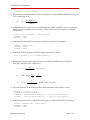
CLKSRCSEL = options->CLKSRC;
3) Determine the multiplier and divider values for the PLLCFG register (MSEL and NSEL) to meet the
core’s requirement for Fcco.
(4)
Fcco =
2 × MSEL × Fosc
NSEL
4) Update the PLLCFG register bits to correspond with these MSEL and NSEL values, as specified in
the LPC23xx User Manual for the desired Fcco. Then, execute a PLL feed sequence to latch this
configuration.
PLLCFG = (options->MSEL | options->NSEL);
PLLFEED = 0xAA;
PLLFEED = 0x55;
5) Enable the PLL with the PLLCON register, and follow with a PLL feed sequence.
PLLCON = PLLCON_PLLE;
PLLFEED = 0xAA;
PLLFEED = 0x55;
6) Monitor the PLOCK bit in the PLLSTAT register until the PLL is locked.
while(!(PLLSTAT & (1 << PLLSTAT_PLOCK)));
7) Determine the divider values required for the core, USB and peripheral clocks (CLK_DIV,
USB_DIV, and PCLK_DIV, respectively).
Fosc
∴ Fcpu ≤ Fcpu , max
CLK _ DIV
(5)
Fcpu =
(6)
USB _ DIV =
(7)
FPERH =
Fosc
Fosc
=
Fusb 48MHz
Fosc
∴ PCLK _ DIV : (1,2,4,8)
PCLK _ DIV
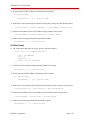
8) Set up the final CPU clock divider (and the USB and peripheral clock dividers, if used).
CCLKCFG = options->CLK_DIV;
USBCLKCFG = options->USB_DIV;
PCLKSEL0 = (options->PCLK_PERH_DIV_1 << options->PCLK_PERH_A);
PCLKSEL1 = (options->PCLK_PERH_DIV_2 << options->PCLK_PERH_B);
9) Enable and connect the PLL with the PLLCON register, and follow with a PLL feed sequence.
PLLCON = (PLLCON_PLLE | PLLCON_PLLC);
PLLFEED = 0xAA;
PLLFEED = 0x55;
Digi-Key Corporation
Page 3 of 7