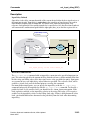
1
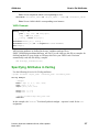
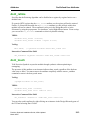
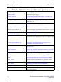
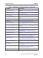
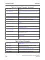
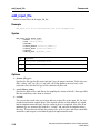
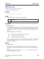
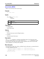
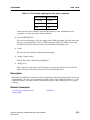
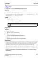
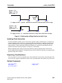
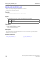
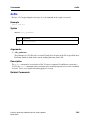
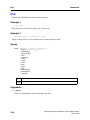
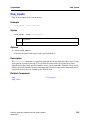
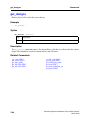
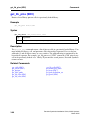
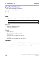
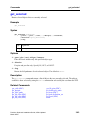
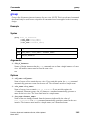
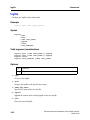
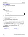
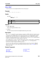
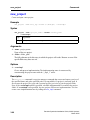
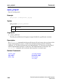
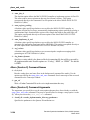
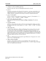
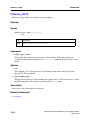
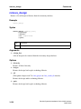
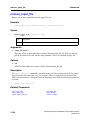
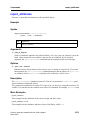
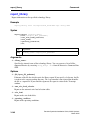
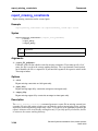
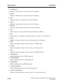
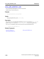
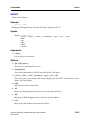
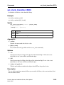
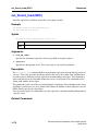
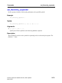
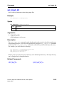
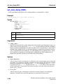
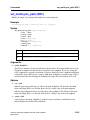
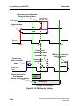
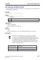
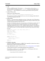
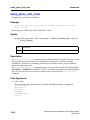
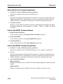
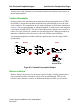
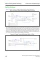
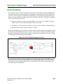
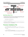
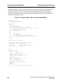
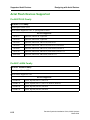
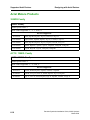
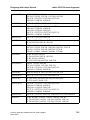
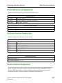
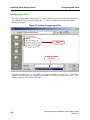
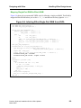
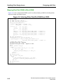
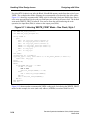
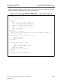
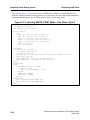
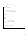
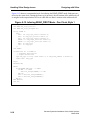
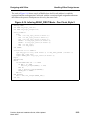
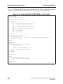
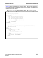
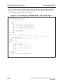
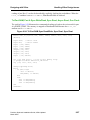
Handling Xilinx Design Issues
Designing with Xilinx
Figure 9-19 shows a style of RAM where the B (read) address is explicitly registered and the
read operation is achieved with the concurrent signal assignment statement that follows the
process. Both ports are driven by the same clock.
Figure 9-19. Inferring NO_CHANGE Mode - One Clock, Style 2
library IEEE;
use IEEE.std_logic_1164.all;
use IEEE.std_logic_unsigned.all;
entity V2RAM is
port(
DOA : out std_logic_vector(3 downto 0);
DIA : in std_logic_vector(3 downto 0);
DOB : out std_logic_vector(3 downto 0);
ADDRA : in std_logic_vector(12 downto 0);
ADDRB : in std_logic_vector(12 downto 0);
WEA : in std_logic;
CLK : in std_logic);
end V2RAM;
architecture rtl of V2RAM is
type mem_type is array (8191 downto 0) of STD_LOGIC_VECTOR (3 downto 0);
signal mem : mem_type;
signal ADDRB_INT : std_logic_vector(12 downto 0);
begin
PROCESS(CLK)
BEGIN
IF CLK'EVENT AND CLK = '1' THEN
IF WEA = '1' THEN
mem(conv_integer(ADDRA)) <= DIA;
ELSE
DOA <= mem(conv_integer(ADDRA));
END IF;
ADDRB_INT <= ADDRB;
END IF;
END PROCESS;
DOB <= mem(conv_integer(ADDRB_INT));
end rtl;
9-22
Precision Synthesis Installation Guide, 2003c Update1
March 2004