1
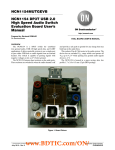
NCP1090GEVB,
NCP1094GEVB
Power-over-Ethernet PD
Interface Evaluation Board
User's Manual
http://onsemi.com
EVAL BOARD USER’S MANUAL
Introduction
The NCP1090GEVB and NCP1094GEVB evaluation
boards are designed to showcase the features of the
NCP109x series of Power-over-Ethernet interfaces. The
boards are designed as splitter interfaces, taking a
PoE-enabled port as input and offering the power to a
separate connector, while passing through the data to
another Ethernet port. The schematics, gerber files and
BOM of these boards are available through our website
(www.onsemi.com)
Basic Circuit Description
The evaluation boards consist of different sections that
will be described in detail in the next paragraphs. First, we
will discuss the input section, including selection of the
correct connectors, magnetics and the termination for a
Power-over-Ethernet enabled connection. In the next
section we will explain the operation of the NCP109x, the
detection and classification process, and how to configure
the NCP109x for the correct power class. Finally, we will
explain how to use the UVLO support (for NCP1091 and
NCP1093) or auxiliary support (for NCP1092 and
NCP1094).
Figure 1. NCP1090GEVB Photo
Table 1. ELECTRICAL CHARACTERISTICS
NCP1090,
NCP1091,
NCP1092
Input Voltage, PoE
NCP1093,
NCP1094
37 V − 57 V
Input Current, PoE
500 mA
680 mA
Auxiliary Input Voltage
7.5 V − 65 V
Auxiliary Input Current
0−5A
Figure 2. NCP1094GEVB Photo
www.BDTIC.com/ON/
© Semiconductor Components Industries, LLC, 2012
October, 2012 − Rev. 0
1
Publication Order Number:
EVBUM2156/D
NCP1090GEVB, NCP1094GEVB
INPUT SECTION
Ethernet Connectors, Magnetics and Termination
Output Connector
Auxiliary Power Connector
Ethernet Connector (out)
Power−over−Ethernet
Connector (in)
Figure 3. Connection Diagram
output connector is connected to a proper
Power-over-Ethernet PSE, the PD detection will fail without
damaging the board, and no power will be applied. When
power is applied across the pairs of this second connector
without negotiation, the board will burn out the termination
resistors.
The NCP109x evaluation boards have 2 RJ45 connectors.
One connector is used as the input connector and supports
Power-over-Ethernet. The power from this connector is split
off to the NCP109x while the Ethernet data is passed through
to the other RJ45 connector. Please note that this second
connector will not support Power-over-Ethernet. When the
Data Pair
Data Pair
Data Pair
Data Pair
Data Pair
Data Pair
Data Pair
Data Pair
Powered
Device
(PD)
Power
Sourcing
Equipment
(PSE)
Figure 4. Ethernet Connection with Power−over−Ethernet
IEEE802.3-af standard and 600 mA for the IEEE802.3-at
standard) without high losses. It is recommended to choose
magnetics that include common- mode chokes to reduce
electromagnetic emissions. When board space is critical, it
can be interesting to choose connectors with build-in
magnetics (‘MagJack’). These connectors also integrate the
termination of the Ethernet line. Contact your magnetics
manufacturer for more information on magnetics suitable
for PoE.
Ethernet connections are double isolated, which means
the data passes through a signal transformer on both on the
Power Supply Equipment (PSE) side as well as on the
Powered Device (PD) side. In the case that the port must
support Power-over-Ethernet, specific signal transformers
must be selected. First, the signal transformers must have a
central tap to access the common mode voltage of each pair,
as these are the carriers for the PoE power. Second, care must
be taken to select transformers that can support the dc
common mode current required (up to 350 mA for the
www.BDTIC.com/ON/
http://onsemi.com
2
NCP1090GEVB, NCP1094GEVB
Figure 5. Input Section of the Evaluation Boards
Termination
Termination of an Ethernet port should be done on the
connector side of the magnetics. The typical termination for
Ethernet ports is called a ‘Bob Smith termination’ and is
shown in Figure 6.
For ports that are Power-over-Ethernet, this termination
network should be modified to block the DC common mode
voltage between pairs from creating a large current through
the termination resistors, which would blow up the
termination resistors. This is done by inserting 10 nF
blocking capacitors in series with the termination resistors.
The modified termination network is shown in Figure 7.
Figure 7. Modified Bob−Smith Termination
Rectification and Protection
Power applied to the Ethernet pairs has no defined polarity
and thus needs to be rectified by diode bridges. The diode
selection is important for the total efficiency of the system,
as the forward voltage drop of the diode can be quite large.
For this reason, discrete schottky diodes are a common
choice for the rectification bridge. To comply with ESD
protection guidelines, a TVS should be added to the rectified
power lines. In the evaluation boards, the 1SMA58AT3G
was selected for this part.
Figure 6. Bob−Smith Termination
www.BDTIC.com/ON/
http://onsemi.com
3
NCP1090GEVB, NCP1094GEVB
NCP109x OPERATION
Power−over−Ethernet Detection and Classification
When the PSE has detected a valid PD signature, the PSE
will start the classification phase. During the classification
phase, the PSE will determine the power class of the PD.
This is determined by measuring the current drawn when a
voltage pulse of typically 17.5 V is applied. Class 4 is only
valid in 802.3at. In 802.3af, class 4 is defined as reserved and
treated as class 0. So to make sure that the PD can distinguish
between at-type PSEs (applying 25.5 W for class 4) and
af-type PSEs (applying 13 W for class 4), the classification
pulse is repeated by the at-type PSE when the PD is
programmed for class 4. This difference is made visible to
external components through the nClassAT pin.
The power class can be programmed by setting the
classification resistor to the correct value. Programming
resistors should be placed as close to the IC as possible to
minimize noise. The different power classes and their
corresponding classification resistors are listed in Table 2.
To distinguish power-over-ethernet enabled ports from
regular Ethernet ports, the Power Supply Equipment (PSE)
will first check the detection signature of the Powered
Device (PD), before negotiating and applying power. The
detection signature is defined as the resistance between
VPORTP and VPORTN, and should be larger than 19 kW
and smaller than 26.5 kW. Typically, a value of 24.9 kW is
used.
The PSE will measure this resistance by making at least
two measurements of the current drawn by the PD while
applying voltages between 2.8 and 10 V. From these
measurements, the PSE will make a linear approximation
from which it will extract the detection resistance.
This means that the total resistance seen at the input of the
PD should be equal to 24.9 kW. During detection, the DET
pin is connected to ground, so for the schematic of the
evaluation board, this means that:
Table 2. PD POWER CLASSIFICATION
(R UVLO1 ) R UVLO2)ńńR det1 + 24.9kW
For the detection and classification to succeed, the total
input capacitance of the PD should be limited to less than
150 nF. When the input capacitance is higher, the capacitor
charge current will influence the detection resistance
measurements, and the detection signature will be invalid.
Under no circumstance is it allowed to connect the bulk
input capacitor (generally in the order of magnitude of
1-10 mF) of the DC/DC convertor to VPORTN. The bulk
input capacitor should always be located on the other side of
the pass switch, and the negative lead should be connected
to RTN. As such, the bulk input capacitor will remain
disconnected during detection, and will not influence the
detection signature.
Once the detection phase is passed, the NCP109x will
disconnect the DET pin to save power that would otherwise
be dissipated in the detection resistor.
Average Input
Power of the PD
Classification
Resistor
0
13 W
4.42 kW
1
3.84 W
953 W
2
6.49 W
549 W
3
13 W
357 W
4*
25.5 W
255 W
Power Class
*Only for NCP1093, NCP1094
After the PSE has detected a valid power class for the PD,
it will apply the full power to the PD.
A typical classification sequence for a class 4 PD is shown
in Figure 8.
Figure 8. PD Classification for Class 4
www.BDTIC.com/ON/
http://onsemi.com
4
NCP1090GEVB, NCP1094GEVB
Inrush and Operational Current Limitation
The pass switch is then turned completely on, and the IC
switches to an operational current limit. Both limits are
programmed with the same programming resistor, which is
connected to ILIM. Programming resistors should be placed
as close to the IC as possible to minimize noise. Typical
values for this programming resistor are shown in Table 3.
When the PSE applies power to the PD after the detection
and classification phases, the pass switch will initially limit
the current passing through it. In this way large currents
caused by the DC/DC convertor input capacitor charging are
prevented.
When the voltage over the pass switch drops below the
limit value, this indicates that the bulk capacitor is charged.
Table 3. PD INPUT CURRENT LIMITS
Average Input Power of the PD
Recommended ILIM Resistor
Inrush Current Limit
Operational Current Limit
13 W
178 kW
120 mA
500 mA
25.5 W
169 kW
120 mA
680 mA
PGOOD Indication
source was connected first. For example, when the auxiliary
is already connected when the Ethernet cable is plugged in,
the auxiliary voltage will interfere with the PoE detection,
and this will result in a dominant auxiliary supply. However,
if the Ethernet cable is connected first, the PoE detection will
be successful, and power will be drawn from the PoE
interface, even if an auxiliary supply is later connected.
It is often desirable for the device to always use the
auxiliary supply, even when PoE is available. In that case,
the PoE must be disabled when the auxiliary is active. This
feature is available in the NCP1092 and NCP1094.
Auxiliary support will disconnect the PoE supply when an
auxiliary supply is connected by disconnecting the internal
pass switch. When not used, the AUX pin of the IC should
be connected to VPORTN. To configure the auxiliary
support dimension the resistor divider connected to the
AUX pin so that the AUX pin voltage is higher than 3.1 V
(typ.) during desired operation. The AUX pin has an internal
pull-down resistor of 100 kW. However, such large
resistance is not desired since a small leakage current can
make the AUX voltage rise very quickly. It is advised to add
an external pull-down resistor of 10 kW. From this we can
dimension Raux1 as follows:
The NCP109x provide a PGOOD signal to indicate when
the power is available for the DC/DC convertor. This is an
open-drain output that is active when the input capacitor has
not completely charged yet. The PGOOD pin is released (to
an external pull-up) when the voltage between RTN and
VPORTN drops below 1 V (typ.).
The intended use for this signal is to connect the PGOOD
signal to the enable pin of your DC/DC controller, to ensure
that the DC/DC controller does not start operation before the
input capacitor is fully charged.
On the evaluation board the PGOOD pin is connected to
a LED. Under normal operation, this LED should only turn
on (briefly) during startup and shutdown.
UVLO Support
All NCP109x ICs have internal UVLO capability, and
will disconnect the pass switch when the VPORTP voltage
becomes too low. The threshold for this is set by an internal
resistor divider to VUVLO,on = 37 V (typ) and VUVLO,off =
31 V (typ).
In addition, the NCP1091 and NCP1093 allow externally
programming the threshold to a different value. If you want
to continue using the default UVLO threshold with the
NCP1091 or NCP1093, connect the UVLO pin to VPORTN.
To enable under-voltage lockout with a different
threshold, you must populate the resistor divider created by
Ruvlo1 and Ruvlo2.This can only be done on the NCP1091
or NCP1093.
The values for these components can be calculated as
follows:
R
) R uvlo2
V uvlo,on + 1.2V uvlo1
R uvlo2
Take also into account that the UVLO resistors will
influence the detection resistance.
R aux1 +
ǒV3.1V *1 Ǔ10kW
aux,on
When the voltage on the AUX pin rises above 3.1 V, the
NCP109x will disable the PoE detection circuit and
disconnect the pass switch, as well as release PGOOD.
To connect the auxiliary support (and have priority of the
auxiliary supply) on the evaluation boards, you must
connect the jumper J1. This is only possible if your
evaluation board has an NCP1092 or NCP1094.
To get an efficient system, it is desirable to have the
forward voltage drop over the auxiliary diode Daux1 as low
as possible, especially since the auxiliary power supply is
often of lower voltage and therefore has less headroom for
voltage drop. This requires a schottky diode. However,
schottky diodes at higher voltages often have a large reverse
leakage current, up to as much as 10mA. If this current were
Auxiliary Support
An auxiliary supply can easily be implemented with a
diode (Daux1). This auxiliary supply is often of a relatively
low voltage (e.g. 24 V). However, this implementation can
result in variable behavior, depending on which power
www.BDTIC.com/ON/
http://onsemi.com
5
NCP1090GEVB, NCP1094GEVB
to flow through the auxiliary resistor divider, the AUX pin
voltage would rise above the threshold, and turn of the PoE,
even when no auxiliary supply is available. For this reason,
we put a PMOS transistor (Q1) in series, which will disable
this current path. The resulting schematic is shown in
Figure 9.
Figure 9. Auxiliary Supply Circuit
nClass_AT
To signal if the PSE went through the 2 event classification,
and the full 25.5W is indeed available, the NCP1093 and
NCP1094 offer the nClass_AT signal. This pin has an open
drain output that is pulled low when two classification
events have occurred.
The NCP1093 and NCP1094 are capable of classifying as
class 4 as per the 802.3at standard, delivering up to 25.5 W.
If the PD is connected to a PSE complying with the
802.3af standard, the PSE will apply power after one
classification event, but this power will be limited to 13 W.
ON Semiconductor and
are registered trademarks of Semiconductor Components Industries, LLC (SCILLC). SCILLC owns the rights to a number of patents, trademarks,
copyrights, trade secrets, and other intellectual property. A listing of SCILLC’s product/patent coverage may be accessed at www.onsemi.com/site/pdf/Patent−Marking.pdf. SCILLC
reserves the right to make changes without further notice to any products herein. SCILLC makes no warranty, representation or guarantee regarding the suitability of its products for any
particular purpose, nor does SCILLC assume any liability arising out of the application or use of any product or circuit, and specifically disclaims any and all liability, including without
limitation special, consequential or incidental damages. “Typical” parameters which may be provided in SCILLC data sheets and/or specifications can and do vary in different applications
and actual performance may vary over time. All operating parameters, including “Typicals” must be validated for each customer application by customer’s technical experts. SCILLC
does not convey any license under its patent rights nor the rights of others. SCILLC products are not designed, intended, or authorized for use as components in systems intended for
surgical implant into the body, or other applications intended to support or sustain life, or for any other application in which the failure of the SCILLC product could create a situation where
personal injury or death may occur. Should Buyer purchase or use SCILLC products for any such unintended or unauthorized application, Buyer shall indemnify and hold SCILLC and
its officers, employees, subsidiaries, affiliates, and distributors harmless against all claims, costs, damages, and expenses, and reasonable attorney fees arising out of, directly or indirectly,
any claim of personal injury or death associated with such unintended or unauthorized use, even if such claim alleges that SCILLC was negligent regarding the design or manufacture
of the part. SCILLC is an Equal Opportunity/Affirmative Action Employer. This literature is subject to all applicable copyright laws and is not for resale in any manner.
PUBLICATION ORDERING INFORMATION
LITERATURE FULFILLMENT:
Literature Distribution Center for ON Semiconductor
P.O. Box 5163, Denver, Colorado 80217 USA
Phone: 303−675−2175 or 800−344−3860 Toll Free USA/Canada
Fax: 303−675−2176 or 800−344−3867 Toll Free USA/Canada
Email: [email protected]
N. American Technical Support: 800−282−9855 Toll Free
USA/Canada
Europe, Middle East and Africa Technical Support:
Phone: 421 33 790 2910
Japan Customer Focus Center
Phone: 81−3−5817−1050
ON Semiconductor Website: www.onsemi.com
Order Literature: http://www.onsemi.com/orderlit
For additional information, please contact your local
Sales Representative
www.BDTIC.com/ON/
http://onsemi.com
6
EVBUM2156/D