1
CE6231 - COFDM demodulator with
USB interface for PC-TV
User Manual
March 29, 2007
Revision 1,2
Reference Number: D73701-003
Legal Statements
INFORMATION IN THIS DOCUMENT IS PROVIDED IN CONNECTION WITH INTEL PRODUCTS. NO LICENSE,
EXPRESS OR IMPLIED, BY ESTOPPEL OR OTHERWISE, TO ANY INTELLECTUAL PROPERTY RIGHTS IS
GRANTED BY THIS DOCUMENT. EXCEPT AS PROVIDED IN INTEL'S TERMS AND CONDITIONS OF SALE FOR
SUCH PRODUCTS, INTEL ASSUMES NO LIABILITY WHATSOEVER, AND INTEL DISCLAIMS ANY EXPRESS OR
IMPLIED WARRANTY, RELATING TO SALE AND/OR USE OF INTEL PRODUCTS INCLUDING LIABILITY OR
WARRANTIES RELATING TO FITNESS FOR A PARTICULAR PURPOSE, MERCHANTABILITY, OR
INFRINGEMENT OF ANY PATENT, COPYRIGHT OR OTHER INTELLECTUAL PROPERTY RIGHT.
Intel products are not intended for use in medical, life saving, life sustaining applications.
Intel may make changes to specifications and product descriptions at any time, without notice.
Designers must not rely on the absence or characteristics of any features or instructions marked “reserved” or
“undefined.” Intel reserves these for future definition and shall have no responsibility whatsoever for conflicts or
incompatibilities arising from future changes to them.
This manual may contain design defects or errors known as errata, which may cause the product to deviate from
published specifications. Current characterized errata are available on request.
This manual as well as the software described in it, is furnished under license and may only be used or copied in
accordance with the terms of the license. The information in this document is furnished for informational use only, is
subject to change without notice, and should not be construed as a commitment by Intel Corporation. Intel
Corporation assumes no responsibility or liability for any errors or inaccuracies that may appear in this document or
any software that may be provided in association with this document.
Except as permitted by such license, no part of this document may be reproduced, stored in a retrieval system, or
transmitted in any form or by any means without the express written consent of Intel Corporation.
Contact your local Intel sales office or your distributor to obtain the latest specifications and before placing your
product order.
Copies of documents which have an ordering number and are referenced in this document, or other Intel literature
may be obtained by calling 1-800-548-4725 or by visiting Intel's website at http://www.intel.com.
BunnyPeople, Celeron, Celeron Inside, Centrino, Centrino logo, Chips, Core Inside, Dialogic, EtherExpress, ETOX,
FlashFile, i386, i486, i960, iCOMP, InstantIP, Intel, Intel logo, Intel386, Intel486, Intel740, IntelDX2, IntelDX4,
IntelSX2, Intel Core, Intel Inside, Intel Inside logo, Intel. Leap ahead., Intel. Leap ahead. logo, Intel NetBurst, Intel
NetMerge, Intel NetStructure, Intel SingleDriver, Intel SpeedStep, Intel StrataFlash, Intel Viiv, Intel XScale, IPLink,
Itanium, Itanium Inside, MCS, MMX, MMX logo, Optimizer logo, OverDrive, Paragon, PDCharm, Pentium, Pentium II
Xeon, Pentium III Xeon, Performance at Your Command, Pentium Inside, skoool, Sound Mark, The Computer Inside.,
The Journey Inside, VTune, Xeon, Xeon Inside and Xircom are trademarks or registered trademarks of Intel
Corporation or its subsidiaries in the United States and other countries.
MPEG is an international standard for video compression/decompression promoted by ISO. Implementations of
MPEG CODECs, or MPEG enabled platforms may require licenses from various entities, including Intel Corporation.
*Other names and brands may be claimed as the property of others.
Copyright © 2006, Intel Corporation
2
CE6231 User Manual
Ref# D73701-003
Contents
1
Introduction ........................................................................................................... 13
1.1
2
3
Related Documents ...................................................................................................................... 13
System ................................................................................................................... 14
2.1
Features........................................................................................................................................ 14
2.2
Applications .................................................................................................................................. 15
Pin definitions........................................................................................................ 17
3.1.1
3.1.2
Pull-Up / Pull-Down Resistors ............................................................................................... 18
Hardware Reset..................................................................................................................... 18
4
Pin diagram............................................................................................................ 19
5
Pin list .................................................................................................................... 20
6
Application schematic .......................................................................................... 21
7
8051 Microprocessor ............................................................................................ 22
7.1
8
Special Function Registers .................................................................................. 24
8.1
9
Internal data memory.................................................................................................................... 22
SFR Summary Table .................................................................................................................... 24
SFR descriptions................................................................................................... 28
9.1
SP - Stack Pointer ........................................................................................................................ 28
9.2
PSW – Program Status Word....................................................................................................... 29
9.3
ACC - Accumulator ....................................................................................................................... 30
9.4
B register ...................................................................................................................................... 31
9.5
MPAGE......................................................................................................................................... 32
9.6
PCON - Power Control ................................................................................................................. 33
9.7
CKCON - Clock Control................................................................................................................ 34
9.8
SPC_FNC – Special function ....................................................................................................... 35
9.9
Dual Data Pointers........................................................................................................................ 36
9.9.1
DPS - Data Pointer Select..................................................................................................... 36
9.9.2
DP0 - Data Pointer Zero........................................................................................................ 37
9.9.3
DP1 - Data Pointer One ........................................................................................................ 37
9.10
Timers/Counters........................................................................................................................ 38
9.10.1 TMOD .................................................................................................................................... 38
9.10.2 TCON - Timer/Counter Control ............................................................................................. 39
9.10.3 Timer0 ................................................................................................................................... 40
9.10.4 Timer1 ................................................................................................................................... 40
9.10.5 T2CON – Timer 2 control ...................................................................................................... 41
9.10.6 RCAP2 – Timer 2 Reload/Capture value ............................................................................. 42
Ref# D73701-003
CE6231 User Manual
3
9.10.7
T2 – Timer two count............................................................................................................ 43
9.11
Interrupts ................................................................................................................................... 44
9.11.1 Interrupt Processing .............................................................................................................. 45
9.11.2 Interrupt Masking................................................................................................................... 45
9.11.3 Interrupt Priorities .................................................................................................................. 46
9.11.4 Interrupt Sampling ................................................................................................................. 48
9.11.5 Interrupt Latency.................................................................................................................... 48
9.11.6 EXIF – Extended Interrupt Flags ........................................................................................... 49
9.11.7 EIE – Extended Interrupt Enable........................................................................................... 50
9.11.8 EIP – Extended Interrupt Priority........................................................................................... 51
9.11.9 IE – Interrupt Enable ............................................................................................................. 52
9.11.10
IP – Interrupt Priority.......................................................................................................... 53
9.11.11
INT1 – Interrupt 1............................................................................................................... 54
9.11.12
INT_EN1 ............................................................................................................................ 55
9.11.13
INT4A................................................................................................................................. 56
9.11.14
INT_EN4A.......................................................................................................................... 57
9.11.15
INT4B................................................................................................................................. 58
9.11.16
INT_EN4B.......................................................................................................................... 59
9.11.17
INT_CTRL.......................................................................................................................... 60
9.11.18
EICON – USB suspend interrupt ....................................................................................... 61
9.12
USB Control and Status Registers............................................................................................ 62
9.12.1 UDM_STATUS ...................................................................................................................... 62
9.12.2 USB_STATUS0 ..................................................................................................................... 63
9.12.3 USB_STATUS1 ..................................................................................................................... 64
9.12.4 USB_STATUS2 ..................................................................................................................... 65
9.12.5 USBC_STATUS3/4 ............................................................................................................... 66
9.12.6 SUSP_CTRL ......................................................................................................................... 67
9.12.7 DISCON_CTRL ..................................................................................................................... 68
9.12.8 EP_8051_CMD – End point command ................................................................................. 69
9.12.9 EP0 – End point 0 control...................................................................................................... 70
9.12.10
EP0_LENGTH.................................................................................................................... 71
9.12.11
EP1 – End point 1 control .................................................................................................. 72
9.12.12
CSR_CMD ......................................................................................................................... 72
9.12.13
CSR_ADDR ....................................................................................................................... 73
9.12.14
CSR_DATA........................................................................................................................ 73
9.13
PID Filters ................................................................................................................................. 74
9.13.1 PF_EN – Data stream/PID filter enable ................................................................................ 74
9.13.2 PID_INT................................................................................................................................. 75
9.13.3 PID_EXT................................................................................................................................ 76
9.13.4 PID_SETUP........................................................................................................................... 77
9.13.5 PF_Header ............................................................................................................................ 78
9.13.6 PF_HEADER_LEN – PF header length ................................................................................ 79
9.13.7 PF_MISC ............................................................................................................................... 80
9.14
4
Two Wire Bus............................................................................................................................ 81
CE6231 User Manual
Ref# D73701-003
9.14.1
9.14.2
9.14.3
9.14.4
9.14.5
9.14.6
TWB_STATUS – Two wire bus status .................................................................................. 81
TWB_GPP_CTRL_RD – Two wire bus status ...................................................................... 82
TWB_CMD – 2-wire bus commands ..................................................................................... 83
TWB_DATA ........................................................................................................................... 84
TWB_SRC ............................................................................................................................. 85
TWB_GPP_CTRL_WR ......................................................................................................... 86
9.15
General Purpose Ports ............................................................................................................. 87
9.15.1 GPP_DIR............................................................................................................................... 87
9.15.2 GPP_DATA ........................................................................................................................... 88
9.16
10
DEMOD_STATUS..................................................................................................................... 89
Demodulator Functional Description ............................................................... 90
10.1
Analogue-to-Digital Converter................................................................................................... 91
10.2
Automatic Gain Control............................................................................................................. 91
10.3
IF to Baseband Conversion ...................................................................................................... 92
10.4
Adjacent Channel Filtering........................................................................................................ 92
10.5
Interpolation and Clock Synchronisation .................................................................................. 92
10.6
Carrier Frequency Synchronisation .......................................................................................... 92
10.7
Symbol Timing Synchronisation................................................................................................ 92
10.8
Fast Fourier Transform ............................................................................................................. 92
10.9
Common Phase Error Correction.............................................................................................. 93
10.10
Channel Equalisation ................................................................................................................ 93
10.11
Impulse Filtering........................................................................................................................ 93
10.12
Transmission Parameter Signalling (TPS)................................................................................ 93
10.13
De-Mapper ................................................................................................................................ 93
10.14
Symbol and Bit De-Interleaving ................................................................................................ 93
10.15
Viterbi Decoder ......................................................................................................................... 93
10.16
MPEG Frame Aligner ................................................................................................................ 94
10.17
De-interleaver............................................................................................................................ 94
10.18
Reed-Solomon Decoder ........................................................................................................... 94
10.19
De-scrambler............................................................................................................................. 94
10.20
Differences from CE6353.......................................................................................................... 95
11
11.1
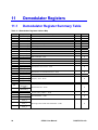
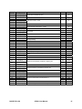
Demodulator Registers...................................................................................... 96
Demodulator Register Summary Table .................................................................................... 96
11.2
Automatic Gain Control (AGC).................................................................................................. 99
11.2.1 System description ................................................................................................................ 99
11.2.2 RF & IF AGC loops.............................................................................................................. 100
11.2.3 Configuring the output voltage limits ................................................................................... 101
11.2.4 Setting the IF/RF crossover point........................................................................................ 102
11.2.5 AGC_TARGETS.................................................................................................................. 104
Ref# D73701-003
CE6231 User Manual
5
11.2.6
11.2.7
11.2.8
11.2.9
11.2.10
11.2.11
11.2.12
11.2.13
11.2.14
11.2.15
11.2.16
11.2.17
11.2.18
AGC_Ctl(_1, _0) .................................................................................................................. 105
AGC_CTL_5 ........................................................................................................................ 106
AGC_Man............................................................................................................................ 107
IF_LoLim.............................................................................................................................. 108
RF_HiLim ......................................................................................................................... 108
IF_Max ............................................................................................................................. 109
IF_Min .............................................................................................................................. 109
RF_Max ........................................................................................................................... 110
RF_Min ............................................................................................................................ 110
KIF ................................................................................................................................... 111
KRF.................................................................................................................................. 111
AGC_GAIN_0, _1 ............................................................................................................ 112
RF_LEVEL ....................................................................................................................... 113
11.3
IF to Baseband Conversion .................................................................................................... 114
11.3.1 INPUT_FREQ_0, _1............................................................................................................ 114
11.3.2 BW_CTL .............................................................................................................................. 115
11.4
Interpolation and Clock Synchronisation ................................................................................ 116
11.4.1 TRL_Nominal_Rate_0, _1................................................................................................... 116
11.5
Carrier Frequency Synchronisation ........................................................................................ 117
11.5.1 CAPT_RANGE .................................................................................................................... 117
11.5.2 AFC_CTL............................................................................................................................. 118
11.5.3 FREQ_OFF_2, _1, _0 ......................................................................................................... 119
11.6
Transmission Parameter Signalling – TPS ............................................................................. 120
11.6.1 Scope of the TPS ................................................................................................................ 120
11.6.2 TPS transmission format ..................................................................................................... 121
11.7
TPS Registers ......................................................................................................................... 122
11.7.1 TPS_GIVEN_1, _0 .............................................................................................................. 125
11.7.2 TPS_CURRENT_0/1........................................................................................................... 126
11.7.3 TPS_RECEIVED_0/1 .......................................................................................................... 127
11.8
TPS identifier........................................................................................................................... 128
11.8.1 TPS_CELL_ID_0/1.............................................................................................................. 128
11.8.2 TPS_MISC_DATA_2, _1, _0............................................................................................... 129
11.9
On-chip timer........................................................................................................................... 130
11.9.1 Programmable Timer Period ............................................................................................... 130
11.9.2 Programmable Timer Value ................................................................................................ 131
11.10 Miscellaneous ......................................................................................................................... 132
11.10.1
FSM_GO.......................................................................................................................... 132
11.10.2
ACQ_CTL ........................................................................................................................ 133
11.10.3
CHIP_ID........................................................................................................................... 134
11.10.4
RESET ............................................................................................................................. 135
11.10.5
OP_CTL_0 ....................................................................................................................... 136
11.10.6
MCLK_CTL ...................................................................................................................... 137
11.10.7
ADC_CTL......................................................................................................................... 138
6
CE6231 User Manual
Ref# D73701-003
11.10.8
FEC_DIS.......................................................................................................................... 139
11.11 Signal-to-Noise ratio ............................................................................................................... 140
11.11.1
SNR ................................................................................................................................. 140
11.12 Error Rate Monitoring.............................................................................................................. 142
11.12.1
RS_ERR_PER_0/1.......................................................................................................... 143
11.12.2
RS_ERR_CNT_2, _1, _0................................................................................................. 144
11.12.3
RS_UBC_0, _1 ................................................................................................................ 145
11.12.4
Viterbi error period – VIT_ERR_PER .............................................................................. 146
11.12.5
VIT_ERR_CNT_2, _1, _0 ................................................................................................ 147
11.13 Status registers ....................................................................................................................... 148
11.13.1
STATUS_0....................................................................................................................... 148
11.13.2
STATUS_1....................................................................................................................... 149
11.13.3
STATUS_3....................................................................................................................... 150
11.14 Status enables ........................................................................................................................ 151
11.14.1
STATUS_EN_0................................................................................................................ 151
11.14.2
STATUS_EN_1................................................................................................................ 152
11.15 Interrupts ................................................................................................................................. 153
11.15.1
INTERRUPT_0 ................................................................................................................ 153
11.15.2
INTERRUPT_1 ................................................................................................................ 154
11.15.3
INTERRUPT_2 ................................................................................................................ 155
11.15.4
INTERRUPT_4 ................................................................................................................ 156
11.15.5
INTERRUPT_5 ................................................................................................................ 157
11.16 INTERRUPT ENABLES.......................................................................................................... 158
11.16.1
INTERRUPT_EN_0 ......................................................................................................... 158
11.16.2
INTERRUPT_EN_1 ......................................................................................................... 159
11.16.3
INTERRUPT_EN_2 ......................................................................................................... 160
11.16.4
INTERRUPT_EN_4 ......................................................................................................... 161
11.17
Elliptic filter .............................................................................................................................. 162
11.18 Carrier Recovery Loop - CRL ................................................................................................. 163
11.18.1
AFC_Step ........................................................................................................................ 163
11.18.2
6MHZ_BW_1 ................................................................................................................... 164
11.18.3
6MHZ_BW_2 ................................................................................................................... 164
11.19 Registers that are not software reset ...................................................................................... 165
11.19.1
CE6231_EN ..................................................................................................................... 166
11.19.2
CLOCK_CTL_0................................................................................................................ 167
11.19.3
CLOCK_CTL_1................................................................................................................ 168
11.19.4
PLL................................................................................................................................... 169
12
USB software description................................................................................ 170
12.1
USB implementation ............................................................................................................... 170
12.1.1 Software endpoint 0 command processing ......................................................................... 171
12.1.2 PC write commands ............................................................................................................ 171
12.1.3 PC read commands............................................................................................................. 172
Ref# D73701-003
CE6231 User Manual
7
12.2
Endpoint 0 example transfer sequences ................................................................................ 173
12.2.1 Class or Vendor command with no data section................................................................. 173
12.2.2 Class or Vendor write command with 10 bytes data ........................................................... 174
12.2.3 Class or Vendor write command with 100 bytes data ......................................................... 175
12.2.4 Class or Vendor read command with 80 bytes data ........................................................... 176
12.2.5 Class or Vendor read command with 1 byte data ............................................................... 177
12.2.6 Software endpoint 1 processing .......................................................................................... 178
12.2.7 USB control and status registers (CSRs)............................................................................ 178
12.2.8 High bandwidth isochronous transfers ................................................................................ 179
12.2.9 Example CSR settings ........................................................................................................ 179
12.2.10
2-wire bus interface ......................................................................................................... 181
12.3
Demodulator register access examples.................................................................................. 182
12.3.1 Enable the demodulator clock and ADC and reset the demodulator .................................. 182
12.3.2 Read the Reed-Solomon error counters ............................................................................. 183
12.3.3 2-Wire bus controller bypass............................................................................................... 184
12.3.4 EEPROM Requirements ..................................................................................................... 184
12.3.4.1 Single address byte format .......................................................................................... 184
12.3.4.2 Dual Address Byte Format ........................................................................................... 185
12.3.5 EEPROM data format.......................................................................................................... 185
12.3.6 Start-up sequence ............................................................................................................... 186
12.3.7 Demodulator start-up sequence .......................................................................................... 186
12.3.8 Acquire channel sequence .................................................................................................. 188
12.4
PID filter programming ............................................................................................................ 190
12.5
Suspend mode ........................................................................................................................ 190
12.5.1 Automatic suspension ......................................................................................................... 191
12.5.2 Software controlled suspension .......................................................................................... 191
12.5.3 Resumption ......................................................................................................................... 192
12.5.4 Demodulator power down ................................................................................................... 192
12.6
Infra-Red detector ................................................................................................................... 192
12.7
CE6231 external inputs........................................................................................................... 193
12.7.1 External DVB Demodulator Input ........................................................................................ 193
12.7.2 External Analog Video and Audio Input .............................................................................. 195
12.7.3 I2S application note............................................................................................................. 195
12.8
Example USB register settings ............................................................................................... 197
12.9
RF level ADC .......................................................................................................................... 200
12.10
Power down ............................................................................................................................ 200
12.11
Calibration ............................................................................................................................... 200
13
8
Electrical characteristics ................................................................................. 201
13.1
Recommended Operating Conditions..................................................................................... 201
13.2
Absolute Maximum Ratings .................................................................................................... 201
13.3
DC Electrical Characteristics .................................................................................................. 202
CE6231 User Manual
Ref# D73701-003
13.4
Crystal specification ................................................................................................................ 203
13.5
Dynamic characteristics .......................................................................................................... 203
14
Package Information ........................................................................................ 204
List of Figures
Figure 1 Watch and record DVB-T system ................................................................................................. 15
Figure 2 Analog and digital TV system ....................................................................................................... 15
Figure 3 Block diagram ...............................................................................................................................16
Figure 4 80-Pin QFP Package Diagram ..................................................................................................... 19
Figure 5 Typical application schematic ....................................................................................................... 21
Figure 6 Internal RAM organisation ............................................................................................................ 23
Figure 7 Interrupts used by the CE6231 ..................................................................................................... 47
Figure 8 OFDM demodulator diagram ........................................................................................................ 90
Figure 9 FEC block diagram ....................................................................................................................... 91
Figure 10 CE6231 AGC internal system outline ......................................................................................... 99
Figure 11 CE6231 system outline............................................................................................................. 100
Figure 12 AGC control range .................................................................................................................... 101
Figure 13 System gain v RF signal level................................................................................................... 102
Figure 14 RF level input buffer.................................................................................................................. 113
Figure 15 TPS parameter usage............................................................................................................... 123
Figure 16 Acquisition/Re-acquisition flow diagram ................................................................................... 124
Figure 17 Single address byte format ....................................................................................................... 184
Figure 18 Dual address byte format.......................................................................................................... 185
Figure 19 Start-up sequence .................................................................................................................... 187
Figure 20 Channel acquisition................................................................................................................... 189
Figure 21 Parallel data format................................................................................................................... 193
Figure 22 Serial data format...................................................................................................................... 194
Figure 23 I2S data re-alignment ............................................................................................................... 195
Figure 24 I2S data format ......................................................................................................................... 196
Ref# D73701-003
CE6231 User Manual
9
List of Tables
Table 1.1 Document References ................................................................................................................ 13
Table 5.1 Package Pin List ......................................................................................................................... 20
Table 9.1 Register bank selection............................................................................................................... 29
Table 9.2 Timer 0/1 mode ........................................................................................................................... 38
Table 9.3 CE6231 internal event interrupts ................................................................................................ 44
Table 9.4 Interrupt Natural Vectors and Priorities....................................................................................... 45
Table 9.5 Summary of interrupt sources, flags, enables, and priority control............................................. 45
Table 11.1 AGC voltage limit setting......................................................................................................... 101
Table 11.2 AGC gain setting ..................................................................................................................... 102
Table 11.3 ITBFREQ................................................................................................................................. 114
Table 11.4 Elliptic filter options ................................................................................................................. 115
Table 11.5 Capture range ......................................................................................................................... 117
Table 11.6 TPS signaling information ....................................................................................................... 121
Table 11.7 TPS_RECEIEVED data format (not including ETSI 300-744 Annex F - DVB-H modes) ....... 121
Table 11.8 TPS_GIVEN data format (not including ETSI 300-744 Annex F - DVB-H modes)................. 125
Table 11.9 TPS_GIVEN data format (not including ETSI 300-744 Annex F - DVB-H modes)................. 126
Table 11.10 Mapping of the cell_id on the TPS bits ................................................................................. 128
Table 11.11 MCLK control ........................................................................................................................ 137
Table 11.12 Table of SNR values ............................................................................................................. 141
Table 11.13 Elliptic filter options ............................................................................................................... 162
Table 11.14 Available clock modes .......................................................................................................... 167
Table 11.15 Register settings for clock mode........................................................................................... 167
Table 13.1 Recommended operating conditions ...................................................................................... 201
Table 13.2 Absolute maximum ratings...................................................................................................... 201
Table 13.3 DC electrical characteristics.................................................................................................... 202
Table 13.4 Digital input bus timing............................................................................................................ 203
10
CE6231 User Manual
Ref# D73701-003
Abbreviations and symbols
ACRONYM
Description
ACI
Adjacent Channel Interferer
ACQ
Acquisition
ADC
Analog to Digital Converter
AGC
Automatic Gain Control
BA
Byte Align(er)
BCH
Bose, Chaudhuri & Hocquenghem (coding scheme applied to TPS data)
BDI
Bit Deinterleave
BER
Bit Error Ratio
CAS
Co and Adjacent channel interference suppression
CCI
Co-Channel Interferer
CHC
Channel Corrector
COFDM
Coded Orthogonal Frequency Division Multiplexing
CP
Continuous Pilot
CPE
Common Phase Error
CRL
Carrier recovery loop
CSI
Channel State Information
CSR
Control and Status Registers
DMP
Symbol Demapper
DVB
Digital Video Broadcasting
ETSI
European Telecommunications Standards Institute
FEC
Forward Error Correction
FFT
Fast Fourier Transform
FSM
Finite State Machine
I2S
An audio bus standard
ISR
Interrupt Service Routine
ITB
IF to Baseband Conversion
ITP
Digital interpolator
PID
Packet Identifier
PPM
Pilot Processing Module
REC656
A digital video standard
SCR
Slope corrector
SDI
Symbol Deinterleave
SFR
Special Function Register
SOF
Start of frame
SP
Scattered pilot
SYR
Symbol timing recovery
TPS
Transmission Parameter Signalling
TRL
Timing Recovery Loop
TS
Transport Stream
TWB
2-Wire Bus
UPIF
Micro-Processor interface
USB
Universal Serial Bus
Ref# D73701-003
CE6231 User Manual
11
Revision History
Date
Revision
Reference #
Description
11 September 2006
1.0
Initial release
23 November 2006
29 March 2007
1.1
1.2
Added I”S interface note
Added Theta-JA data
12
CE6231 User Manual
Ref# D73701-003
1
Introduction
1.1
Related Documents
Table 1.1 Document References
Title
Number
Location
Universal Serial Bus Specification, Revision 2.0, 27th April 2000
Universal Serial Bus Device Class Definition for Video Devices, Revision 1.1, 1st
June 2005
Universal Serial Bus Device Class Definition for Video Devices: MPEG2-TS
Payload, Revision 1.1, 1st June 2005
Recommendation ITU-R BT.656-4, 1998
http://www.usb.org/home
http://www.usb.org/developer
s/devclass_docs
http://www.usb.org/developer
s/devclass_docs
http://www.itu.int/
NorDig Unified Requirements for profiles Basic TV, Enhanced, Interactive and
Internet for Digital Integrated Receiver Decoders for use in cable, satellite,
terrestrial and IP-based networks, version 1.0.2
CE6353 DVB-T Demodulator Design Manual – April 2006
http://www.nordig.org/
Ref# D73701-003
CE6231 User Manual
D56169-002
Intel® CE 6353 DVB-T
Demodulator - Overview
13
2
System
2.1
Features
•
•
•
•
•
•
•
•
•
•
•
•
•
•
•
•
•
Nordig Unified and ETSI 300 744 compliant
Superior Single Frequency Network performance
Unique active impulse-noise filtering
Single SAW operation on 6, 7 & 8 MHz OFDM
Excellent performance with any echo profile: pre, post, inside or outside the guard interval
Automatic co-channel and adjacent-channel interference suppression
Fast AGC and good Doppler performance for portable applications
Large frequency capture range to enable channel acquisition with triple offsets
Clock generation from single low-cost 24.0 MHz crystal
IF sampling at 36.17, 43.5 or 5 - 10 MHz from a single crystal frequency
Channel bandwidth of 6, 7 & 8 MHz
Blind acquisition capability (including 2K/8K mode detect)
Automatic spectral inversion detection
Fast auto-acquisition technology
Very low software overhead
Access to channel SNR, pre- and post-Viterbi bit error rates
7-bit ADC for RF signal level measurement
•
•
•
•
•
•
•
USB 2.0 compliant interface, 1.1 compatible
2nd digital input for DVB TS or REC656 + I2S
On-chip 8051 microcontroller with 12K program and 4K data RAM.
Hardware MPEG2 PID filters (enables USB1.1 operation)
Infra-red port for remote control signal decode in software
Self or bus powered modes
8 general purpose ports
•
•
•
•
•
•
Full chip control over USB bus
3.3/1.8V operation
80 pin LQFP
Low external component count
Evaluation board and comprehensive software
Full front end (NIM) reference design available
Applications
•
Hybrid (analog + digital) or twin digital tuner application
•
•
•
Terrestrial PC applications
Digital terrestrial TV set-top boxes
Digital terrestrial integrated televisions
14
CE6231 User Manual
Ref# D73701-003
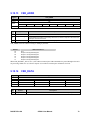
2.2
Applications
The CE6231 is intended for use in a dual tuner system. Figure 1 shows a “watch-and-record” DVB-T system for use
in a recordable media box. This uses an external CE6353as a second DVB-T demodulator.
Figure 1 Watch and record DVB-T system
Figure 2 shows an analog and digital PC TV application. The analog demodulator will generate ITU-656 video data
and I2S audio data for the CE6231 to transfer over the USB.
Figure 2 Analog and digital TV system
Ref# D73701-003
CE6231 User Manual
15
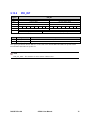
Figure 3 Block diagram
AGC1, AGC2
OFDM
IF input
10 bit
ADC
RF level
input
7 bit
ADC
FEC
System
clocks
Demod
UPIF
Demod PLL
PID filter
1
PID filter
2
MPEG2 TS
ITU656
USB
controller
USB PHY
+ PLL
USB
Buffer
Input
intreface
30MHz clock
I2S
Crystal +
Demod
PLL/ADC
power down
Data RAM
Suspend
control
CLK1/ DATA1
2-wire bus
controller
8051
CLK2/ DATA2
SLEEP
IRDI
GPP[7:0]
Program
RAM
16
CE6231 User Manual
Ref# D73701-003
3
Pin definitions
Pin
Name
External input
1,2,71,74,75
76,77,80
70
Pin description
I/O
Note
mA
MDI(7:0)
External MPEG data input and ITU 656
data input.
I/O
MCLK
MPEG clock or ITU 656 clock input.
I/O
68
MIVAL
I/O
67
MISTART
63
SCK
External MPEG data valid input or
I2S data input.
MPEG packet start pulse or
I2S word select input.
2
I S clock input
I
4
CLK1
EEPROM Master 2-wire bus clock
I/O
5
DATA1
EEPROM Master 2-wire bus data
I/O
27
CLK2
Tuner Master 2-wire bus clock
I/O
28
DATA2
Tuner Master 2-wire bus data
I/O
32
ADFMT
EEPROM address format
I
Open drain
Fall time control
Open drain
Fall time control
Open drain
Fall time control
Open drain
Fall time control
CMOS
59
60
XTIB
XTO
Low phase noise oscillator cell. A 24
MHz crystal must be used
I
I
CMOS
CMOS
GPP(7:0)
General Purpose Ports
I/O
CMOS Tristate / pushpull
3.3
6
AGC1
AGC2
IF AGC o/p
RF AGC o/p, should be tied to ground
when not used
RF AGC level indicator input
O
O
Open drain
Open drain
5
5
6
6
I
Analog
1
I/O
CMOS
Tristate
CMOS
Tristate
CMOS
Tristate
CMOS
Tristate
CMOS
V
3.3
1
3.3
1
3.3
1
3.3
1
3.3
2-wire bus
5
6
5
6
5
6
5
6
3.3
Crystal
GPP’s
3,8,16,17,18
19,20,23,
AGC
24
25
42
RFLEV
29
SLEEP
69
62
Control
O
CMOS
3.3
RESETB
Suspend mode power down for rest of
PCB. High = suspend, low = powered
Active low reset pin
I
CMOS
5
IRDI
Infra-red input
I
CMOS
3.3
USBP
USBM
RES1K5
RES6K2
USB positive data
USB negative data
USB pull up resistor
USB bias resistor
I/O
I/O
I/O
I/O
Differential Analog
Differential Analog
PLLVDD
PLLGND
CVDD
PLL and clocking supply
PLL ground supply
Demodulator core logic power supply
S
S
S
1.8
0
1.8
CUVDD
IVDD
VSS
USB core logic power supply
I/O ring power supply
Logic Core and I/O ground
S
S
S
1.8
3.3
0
Infra-red
USB
47
48
46
55
Digital power
pins
34
35
9,11, 13,
26,56.79
15,57,64
6,21,73
7, 10, 12, 14,
Ref# D73701-003
CE6231 User Manual
3.3
0
17
22, 33, 58,
61,72,78
Pin
Name
Pin description
I/O
Note
V
mA
ADC pins
38
39
AIN
AINB
ADC positive input
ADC negative input
I
I
Differential Analog
Differential Analog
AVDD
AGND
AVD33
DVDD
DGND
ADC analog supply
ADC analog supply
ADC I/O and RF level ADC supply
ADC digital supply
ADC digital ground
S
S
S
S
S
1.8
0
3.3
1.8
0
VDDD33
VDDL18
VDDA33
VSSD
VSSA
USB PHY Digital I/O supply
USB PHY Logic supply
USB PHY Analog supply
USB PHY Digital ground
USB PHY Analog ground
S
S
S
S
S
3.3
1.8
3.3
0
0
TEST
TEST
Test pins
Test pins
I
I
ADC power
pins
36
40, 37
41
44
43
USB power
pins
50
51
45, 53
52
49, 54
TEST
65, 66
30, 31
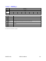
3.1.1
Connect to ground
Connect to VDD33
0
3.3
Pull-Up / Pull-Down Resistors
Pin RES1K5 must be connected to a 1.5 kohm (+/- 5%) resistor tied to 3.3V. This is used for the USB bus pull-up.
Pin RES6K2 must be connected to a 6.2 kohm (+/- 1.0%) resistor tied to ground. This is used to bias the USB band
gap reference. A 0.1 µF capacitor should be connected in parallel with this.
3.1.2
Hardware Reset
At system power up, the hardware reset pin RESETB must be held low for at least 40 ms and no more than 90 ms.
18
CE6231 User Manual
Ref# D73701-003
4
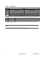
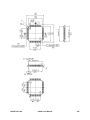
Pin diagram
MDI6/RD6
VSS
61
IRDI
SCK
CUVDD
TEST
65
TEST
MISTART/WS
MIVAL/CD
RESETB
MCLK/RCK
MDI0/RD0
70
VSS
IVDD
MDI1/RD1
MDI2/RD2
MDI3/RD3
75
MDI4/RD4
VSS
CVDD
80
MDI5/RD5
Figure 4 80-Pin QFP Package Diagram
1
60
XTO
MDI7/RD7
XTIB
GPP0
VSS
CLK1
DATA1
CUVDD
5
CVDD
IVDD
55
VSS
VSSA
GPP1
VDDA33
CVDD
VSS
RES6K2
VSSD
CE6231
10
CVDD
VDDL18
50
LQFP 80
VSS
VDDD33
VSSA
CVDD
USBM
VSS
USBP
CUVDD
15
RES1K5
GPP2
45
VDDA33
GPP3
DVDD
GPP4
DGND
GPP5
RFLEV
40
AVDD33
AGND
AIN
AINB
AVDD
AGND
35
PLLVDD
CE6231 User Manual
PLLGND
VSS
ADFMT
TEST
TEST
SLEEP
CLK2
DATA2
AGC2
CVDD
GPP7
AGC1
VSS
IVDD
Ref# D73701-003
30
41
25
20
21
GPP6
19
5
Pin list
Table 5.1 Package Pin List
20
PIN
FUNCTION
PIN
FUNCTION
PIN
FUNCTION
PIN
FUNCTION
1
2
3
4
5
6
7
8
9
10
11
12
13
14
15
16
17
18
19
20
MDI6/RD6
MDI7/RD7
GPP0
CLK1
DATA1
IVDD
VSS
GPP1
CVDD
VSS
CVDD
VSS
CVDD
VSS
CUVDD
GPP2
GPP3
GPP4
GPP5
GPP6
21
22
23
24
25
26
27
28
29
30
31
32
33
34
35
36
37
38
39
40
IVDD
VSS
GPP7
AGC1
AGC2
CVDD
CLK2
DATA2
SLEEP
TEST
TEST
ADFMT
VSS
PLLVDD
PLLGND
AVDD
AGND
AIN
AINB
AGND
41
42
43
44
45
46
47
48
49
50
51
52
53
54
55
56
57
58
59
60
AVD33
RFLEV
DGND
DVDD
VDDA33
RES1K5
USBP
USBM
VSSA
VDDD33
VDDL18
VSSD
VDDA33
VSSA
RES6K2
CVDD
CUVDD
VSS
XTIB
XTO
61
62
63
64
65
66
67
68
69
70
71
72
73
74
75
76
77
78
79
80
VSS
IRDI
SCK
CUVDD
TEST
TEST
MISTART/WS
MIVAL/SD
RESETB
MCLK/RCK
MDI0/RD0
VSS
IVDD
MDI1/RD1
MDI2/RD2
MDI3/RD3
MDI4/RD4
VSS
CVDD
MDI5/RD5
CE6231 User Manual
Ref# D73701-003
6
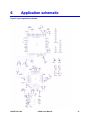
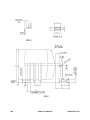
Application schematic
Figure 5 Typical application schematic
Ref# D73701-003
CE6231 User Manual
21
7
8051 Microprocessor
The CE6231 is controlled by an internal 8051-compatible microprocessor. This is connected to 3 internal memories.
The “Internal RAM” is 256 bytes. The “Program RAM” is 12 Kbytes. The “Data RAM” (or “External RAM”) is
4Kbytes. There is no ROM inside the CE6231. The Program RAM can be written-to by the 8051 and by the 2-wire
bus controller. The Data RAM can be written-to and read-from by the USB controller. The Data RAM can be read by
PID Filter.
The 8051 is clocked at 30 MHz and the basic instruction cycle is four 30 MHz cycles. There are 3 timers in the 8051.
There are no serial ports. There are 7 interrupts used in the CE6231:
Name
Sensitive
Purpose
INT0_N
INT1_N
INT2
INT3_N
INT4
INT5_N
Edge
Level
Edge
Edge or level
Level
Edge or level
Infra-red falling edge detection
USB interrupts
Infra-red rising edge detection
Demodulator interrupts
2-wire bus and PID Filter interrupts
External interrupt input from GPP(7)
SUSPI
Level
Suspend interrupt
7.1
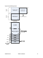
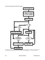
Internal data memory
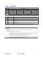
Internal Data Memory is mapped in Figure 6. The memory space is shown divided into three blocks which are
generally referred to as the Lower 128, the Upper 128, and SFR space.
Internal Data Memory addresses are always one byte wide, which implies an address space of only 256 bytes.
However, the addressing modes for internal RAM can in fact accommodate 384 bytes, using a simple trick. Direct
addresses higher than 7FH are one memory space, and indirect addresses higher than 7FH access a different memory
space. Thus Figure 6 shows the Upper 128 and SFR (Special function register) space occupying the same block of
addresses 80H through FFH, although they are physically separate entities.
The lower 128 bytes of RAM are as mapped in Figure 6.
The lowest 32 bytes are grouped into 4 banks of 8 registers (R0 – R7). Two bits in the Program Status Word (PSW)
select which register bank is in use. This allows more efficient use of code space, since register instructions are
shorter than instructions that use direct addressing.
The next 16 bytes above the register bank form a block of bit-addressable memory apace. The 8051 instruction set
includes a selection of single-bit instructions, and the 128 bits in this area can be directly addressed by these
instructions. The bit addresses in this area are 00H through 7FH.
All of the bytes in the Lower 128 can be accessed by either direct or indirect addressing. The Upper 128 can only be
accessed by indirect addressing.
22
CE6231 User Manual
Ref# D73701-003
Figure 6 Internal RAM organisation
FFh
Upper
128
bytes
FFh
Accessible by indirect
addressing only
Accessible by direct
addressing only
80h
7Fh
Lower
128
bytes
80h
7Fh
78h
Accessible by direct and
indirect addressing
20h
Ref# D73701-003
07h
SFR’s
(Special Function Registers)
00h
CE6231 User Manual
23
8
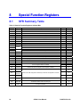
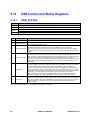
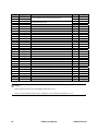
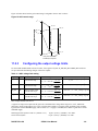
Special Function Registers
8.1
SFR Summary Table
Table 8.1 Special Function Registers Address Map
Address
Symbol
80h
81h
82h
83h
84h
85h
86h
87h
88h
89h
8Ah
8Ch
8Bh
8Dh
8Eh
8Fh
90h
91h
92h
93-99h
9Ah
9Bh
9Ch
Unused
SP
DP0L
DP0H
DP1L
DP1H
DPS
PCON
TCON
TMOD
9Dh
9Eh
9Fh
A0h
A1h
A2h
A3h
24
Timer0
Timer1
CKCON
SPC_FNC
Unused
EXIF
MPAGE
Unused
INT1
INT4A
INT4B
UDM
STATUS
USBC
STATUS0
USBC
STATUS1
USBC
STATUS2
TWB
STATUS
TWB GPP
CTRL RD
EP 8051
CMD
Description
Default
Access
8051 Stack Pointer
Data Pointer Zero – Low byte
Data Pointer Zero – High byte
Data Pointer One – Low byte
Data Pointer One – High byte
Data Pointer Select
Power Control
Timer/Interrupt Control
Timer Mode
Timer Zero Count - Low
Timer One Count – Low
Timer Zero Count – High
Timer One Count – High
Clock Control
Special Function
07H
00H
00h
00h
00h
00h
30h
00h
00h
00h
00h
00h
00h
01h
00h
R/W
R/W
R/W
R/W
R/W
R/W
R/W
R/W
R/W
R/W
R/W
R/W
R/W
R/W
R/W
Extended Interrupt Flags
Memory page, used for 16 bit address transfers with MOVX instructions
08h
00h
R/W
R/W
USB event interrupt register
INT4 interrupt pin is connected to 10 interrupt events, therefore these are split
across 2 registers INT4A and INT4B.
----
R
R
R
Indicates the status of endpoint 0 and endpoint 1 transfers
--
R
--
R
--
R
--
R
Indicates the status of the previous 2-wire bus command
--
R
Contains the status of the 2-wire bus pins
--
R
End point command
00h
R/W
Contains the USB configuration selected by the last Set Configuration command.
CE6231 User Manual
Ref# D73701-003
Address
A4h
A5h
A6h
A7h
A8h
A9h
AAh
ABh
Ach
ADh
AEh
AFh
B0h
B1h
B2h
B3h
B4h
B5h
B6h
B7h
B8h
B9h
BAh
BBh
Symbol
EP0
SETUP
ADDR
EP0
ADDR0
EP0
ADDR1
EP0
LENGTH
IE
EP1
ADDR
EP1
LENGTH0
EP1
LENGTH1
CSR CMD
CSR
ADDR
CSR
DATA0
CSR
DATA1
CSR
DATA2
CSR
DATA3
PF EN
PID INT
BASE
ADDR
PID INT
MAX
PID EXT
BASE
ADDR
PID EXT
MAX
PF INT
MAX LEN
IP
PF EXT
MAX
LEN0
PF EXT
MAX
LEN1
PF I2S
MAX LEN
Ref# D73701-003
Description
Default
Access
00h
R/W
08h
R/W
00h
R/W
00h
R/W
00h
R/W
32h
R/W
00h
R/W
00h
R/W
00h
R/W
00h
R/W
00h
R/W
00h
R/W
00h
R/W
00h
R/W
30h
R/W
12h
R/W
00h
R/W
C0h
R/W
00h
R/W
USB payload setting
00h
R/W
Interrupt priority
80h
R/W
USB payload setting
04h
R/W
USB payload setting
20h
R/W
PF I2S Max Length
30h
R/W
End point zero control
Enables or disables the interrupts in the 8051 core
End point one control
USB control and status
Data stream/PID filter enable
This register pair defines the base address in 32-bit words of the internal MPEG
data PID look-up table and the internal MPEG data PID look-up table size
This register pair defines the base address in 32-bit words of the external MPEG
data PID look-up table and the external MPEG data PID look-up table size
CE6231 User Manual
25
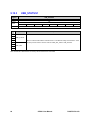
Address
BCh
BDh
BEh
BFh
C0-C1h
C2h
C3-C7h
C8h
C9h
CAh
CBh
CCh
CDh
CE-CFh
D0h
D1h
D2h
D3h
D4h
D5h
D6h
D7h
D8h
D9h
DAh
DBh
DCh
DDh
DEh
DFh
E0h
E1h
E2-E4h
26
Symbol
PF
HEADER0
PF
HEADER1
PF
HEADER2
PF
HEADER3
Reserved
PF
HEADER
LEN
Reserved
T2CON
Reserved
RCAP2L
RCAP2H
TL2
TH2
Reserved
PSW
TWB
CMD
TWB
DATA
TWB SRC
TWB GPP
CTRL WR
INT EN1
INT EN4A
INT EN4B
EICON
INT CTRL
GPP DIR
GPP
DATA
USBC
STATUS3
USBC
STATUS4
PF MISC
SUSP
CTRL
ACC
DISCON
CTRL
Reserved
Description
Default
Access
02h
R/W
80h
R/W
00h
R/W
00h
R/W
PF Header Length
22h
R/W
Timer 2 control
00h
R/W
00h
00h
00h
00h
R/W
R/W
R/W
R/W
Progam status word
00h
R/W
2-wire bus command
00h
R/W
2-wire bus data
00h
R/W
Select the 2-wire bus interface for access by the 2-wire bus controller
01h
R/W
2-wire bus bit control through GPP ports
3Fh
R/W
Enable interrupt one
00h
00h
00h
40h
0Ah
00h
R/W
R/W
R/W
R/W
R/W
R/W
00h
R/W
--
R
--
R
Miscellaneous control bits
C0h
R/W
USB suspend control
0Ch
R/W
Accumulator
00h
R/W
USB disconnect control
50h
R/W
These registers define the header bytes (0 to 4) added to the start of each USB
payload
Timer 2 Reload/Capture value
Timer 2 current count
Enable interrupt 4
USB suspend interrupt
Interrupt control
GPP direction control
Defines the data on each GPP pin
USB status
CE6231 User Manual
Ref# D73701-003
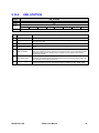
Address
E5h
E6-E7h
E8h
E9-EFh
F0h
F1-F7h
F8h
F9-FFh
Symbol
DEMOD
STATUS
Reserved
EIE
Reserved
B
Reserved
EIP
Reserved
Ref# D73701-003
Description
Default
Access
Demodulator control
18h
R/W
Extended interrupt enable
E0h
R/W
B register
00h
R/W
Extended interrupt priority
E0h
R/W
CE6231 User Manual
27
9
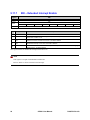
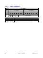
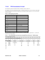
SFR descriptions
This section presents the special function registers information.
9.1
SP - Stack Pointer
Register
Stack Pointer
Access
Address
Default
Bit order
Bit
7:0
Read/Write
81h
07h
0
7
0
0
0
Symbol
SP
0
1
1
1
0
Description
Points to the next available stack location.
This is the 8051 Stack Pointer. The “internal RAM” used for stack storage is 256 bytes. The Stack Pointer Register is
8 bits wide. It is incremented before data is stored during PUSH and CALL executions. While the stack may reside
anywhere in on chip RAM, the Stack Pointer is initialized to 07h after a reset. This causes the stack to begin at
location 08h.
28
CE6231 User Manual
Ref# D73701-003
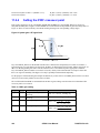
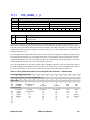
9.2
PSW – Program Status Word
Register
PSW
Access
Address
Read/Write
D0h
00h
Default
0
7
Bit order
Bit
5
F0
4:3
0
0
0
0
0
0
Description
Carry flag. Bit 7 is set to 1 when last arithmetic operation resulted in a carry (during addition) or
borrow (during subtraction); otherwise cleared to 0 by all arithmetic operations.
Auxiliary carry flag. Bit 6 is set to 1 when last arithmetic operation resulted in a carry into (during
addition) or borrow from (during subtraction) the high-order nibble; otherwise cleared to 0 by all
arithmetic operations.
User flag 0. Bit 5 is a bit-addressable, general purpose flag for software control.
AC
6
0
Symbol
CY
7
0
RS [1:0]
Register bank select. Bits 4:3 select the current register bank to use as given in the table below.
2
OV
Overflow flag. Bits 2 is set to 1 when last arithmetic operation resulted in a carry (addition), borrow
(subtraction), or overflow (multiply or divide); otherwise cleared to 0 by all arithmetic operations.
1
F1
User flag 1. Bit 1 is a bit-addressable, general purpose flag for software control.
0
P
Parity flag. Bit 0 is set to 1 when modulo-2 sum of 8 bits in accumulator is 1 (odd parity); cleared to 0
on even parity.
The Program Status Word (PSW) contains several status bits that reflect the current state of the CPU. The PSW,
shown in below, resides in SFR space. It contains the Carry bit, the Auxiliary Carry (for BCD operations), the two
register bank select bits, the Overflow flag, a Parity bit, and two user-definable status flags.
The Carry bit, other than serving the functions of a Carry bit in arithmetic operations, also serves as the
“Accumulator” for a number of Boolean operations.
The bits RSO and RSl are used to select one of the four register banks shown in Table 9.1. A number of instructions
refer to these RAM locations as RO through R7. The selection of which of the four banks is being referred to is made
on the basis of the bits RSO and RS1 at execution time.
The Parity bit reflects the number of 1s in the Accumulator: P = 1 if the Accumulator contains an odd number of 1s,
and P = O if the Accumulator contains an even number of 1s. Thus the number of 1s in the Accumulator plus P is
always even.
Two bits in the PSW are uncommitted and maybe used as general purpose status flags.
Table 9.1 Register bank selection
Bits [4:3] RS1:RS0
00
01
10
11
Ref# D73701-003
Bank selected
Register bank 0, RAM addresses 00h–07h
Register bank 1, RAM addresses 08h–0Fh
Register bank 2, RAM addresses 10h–17h
Register bank 3, RAM addresses 18h–1Fh
CE6231 User Manual
29
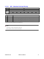
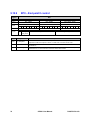
9.3
ACC - Accumulator
Register
ACC
Access
Address
Default
Bit order
Bit
7:0
Read/Write
E0h
00h
0
7
0
Symbol
ACC
0
0
0
0
0
0
0
Description
Accumulator.
This is the accumulator register.
30
CE6231 User Manual
Ref# D73701-003
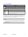
9.4
B register
Register
B
Access
Address
Default
Bit order
Bit
7:0
Read/Write
F0h
00h
0
7
0
Symbol
B
0
0
0
0
0
0
0
Description
The B register.
The B register is used during multiply and divide operations. For other instructions it can be treated as another scratch
pad register.
Ref# D73701-003
CE6231 User Manual
31
9.5
MPAGE
Register
MPAGE
Access
Address
Read/Write
92h
00h
Default
0
7
Bit order
Bit
7:0
32
Symbol
MPAGE
0
0
0
0
0
0
0
0
Description
This register contains the upper address byte used during MOVX A, @Ri and MOVX @Ri, A
opcodes.
CE6231 User Manual
Ref# D73701-003
9.6
PCON - Power Control
Register
PCON
Access
Address
Read/Write
87h
30h
Default
0
7
Bit order
Bit
7:4
0
1
Symbol
1
0
0
0
0
0
Description
-
Reserved
3
GF1
General purpose flag 1. Bit-addressable, general purpose flag for software control.
2
GF0
General purpose flag 1. Bit-addressable, general purpose flag for software control.
1
STOP
When set to 1, the 8051 is placed into stop mode
0
IDLE
When set to 1, the 8051 is placed into idle mode
The CE6231 provides two power saving modes: idle mode and stop mode.
Idle mode:
Exit idle mode by interrupt or reset.
Stop mode:
Exit stop mode by power-on reset only.
Ref# D73701-003
CE6231 User Manual
33
9.7
CKCON - Clock Control
Register
Register name
Access
Address
Read/Write
8Eh
01h
Default
0
7
Bit order
Bit
7:6
0
Symbol
0
0
0
0
0
1
0
Description
-
Reserved
5
T2M
When bit 5 is 1, Timer 2 uses CLK_30 / 4. When 0, Timer 2 uses CLK_30 / 12.
4
T1M
When bit 4 is 1, Timer 1 uses CLK_30 / 4. When 0, Timer 1 uses CLK_30 / 12.
3
T0M
When bit 3 is 1, Timer 0 uses CLK_30 / 4. When 0, Timer 0 uses CLK_30 / 12.
6
2:0
CKMD
Bits 2:0 should be set 0.
This register sets the division ratio of the 30MHz clock and thus determines the clock to be used for the timers T0, 1
and 2.
Note
Bits 2:0 should be set 0. This should be done as the first operation of the user software.
34
CE6231 User Manual
Ref# D73701-003
9.8
SPC_FNC – Special function
Register
SPC_FNC
Access
Address
Read/Write
8Fh
00h
Default
0
7
Bit order
Bit
7:1
0
0
Symbol
0
0
0
0
0
0
0
Description
-
Reserved
WRS
When bit 0 is 1, instructions that normally write to Data RAM, write to Program RAM instead. When
bit 0 is 0, these opcodes access the Data RAM.
This affects MOVX @DTPR and MOVX @Ri opcodes. This feature can be used to provide software modifications
via the USB. Care must be taken if MOVX opcodes are used in interrupt service routines.
Ref# D73701-003
CE6231 User Manual
35
9.9
Dual Data Pointers
The CE6231 employs dual data pointers to accelerate data memory block moves. The standard 8051 data pointer
(DPTR) is a 16-bit value used to address external data RAM or peripherals. The CE6231 maintains the standard data
pointer as DPTR0 at SFR locations 82h and 83h. It is not necessary to modify code to use DPTR0.
The CE6231 adds a second data pointer (DPTR1) at SFR locations 84h and 85h. The SEL bit in the DPTR Select
register, DPS (SFR 86h), selects the active pointer. When SEL = 0, instructions that use the DPTR will use DPL0 and
DPH0. When SEL = 1, instructions that use the DPTR will use DPL1 and DPH1. SEL is the bit 0 of SFR location
86h. No other bits of SFR location 86h are used.
All DPTR-related instructions use the currently selected data pointer. To switch the active pointer, toggle the SEL bit.
The fastest way to do so is to use the increment instruction (INC DPS). This requires only one instruction to switch
from a source address to a destination address, saving application code from having to save source and destination
addresses when doing a block move. When bit 0 is 1, DPH1 and DPL1 are the data pointers. When 0, DPH0 and
DPL0 are the data pointers.
Using dual data pointers provides significantly increased efficiency when moving large blocks of data.
The SFR locations related to the dual data pointers are:
● 82h – DP0L Data Pointer zero low byte
● 83h – DP0H Data Pointer zero high byte
● 84h – DP1L Data Pointer one low byte
● 85h – DP1H Data Pointer one high byte
● 86h - DPS Data Pointer Select (LSB)
9.9.1
DPS - Data Pointer Select
Register
DPS
Access
Address
Default
Bit order
Bit
7:1
0
36
Read/Write
86h
00
0
7
0
Symbol
0
0
0
0
0
0
0
Description
-
Reserved
DPS
Selects between data pointer zero and one.
CE6231 User Manual
Ref# D73701-003
9.9.2
DP0 - Data Pointer Zero
Register
DP0
Access
Symbol
Address
Read/Write
DP0L
82h
Default
DP0H
83h
00h
Bit order
Bit
0
15
0
0
0
00h
0
0
0
0
0
8
Symbol
15:0
0
0
0
0
7
0
DP1 - Data Pointer One
Register
DP1
Access
Symbol
Address
Default
Read/Write
DP1L
84h
00h
0
0
0
0
DP1H
85h
00h
0
15
DP1
0
0
0
0
8
Symbol
15:0
0
Data pointer zero.
9.9.3
Bit
0
Description
DP0
Bit order
0
0
0
0
0
0
7
0
0
0
Description
Data pointer one.
These dual data pointers can be used to accelerate data memory block moves. The DPS bit in the DPTR Select
register, DPS (SFR 86h), selects the active pointer. When DPS = 0, instructions that use the DPTR will use DPL0 and
DPH0. When DPS = 1, instructions that use the DPTR will use DPL1 and DPH1. DPS is the bit 0 of SFR location
86h. No other bits of SFR location 86h are used.
Using dual data pointers provides significantly increased efficiency when moving large blocks of data.
Note
Bit 0 of DPS (special function register 86h) is used to select between DP0/1.
Ref# D73701-003
CE6231 User Manual
37
9.10
Timers/Counters
9.10.1
TMOD
Register
TMOD
Access
Address
Read/Write
89h
00
Default
0
7
Bit order
Bit
7
5:4
3
2
1:0
0
Symbol
T1GATE
6
0
T1CT
0
0
0
0
0
0
Description
When bit 7 is 1, Timer 1 will only count when INT1_N = 1 and TR1 = 1. When bit 7 is 0, Timer 1 will
count when TR1 = 1.
(SFR 88h, TCON).
Bit 6 should be set to 0 for correct operation.
T1MD[1:0]
Bits 5:4 select the mode of Timer 1 as given below.
T0GATE
When bit 3 is 0, Timer 0 will count if TR0 = 1 (SFR 88h, TCON).
T0CT
Bit 2 should be set to 0 for correct operation.
T0MD[1:0]
Bits 1:0 select the mode of Timer 0 as given below.
Timers 0 and 1 each operate in four modes, as controlled through the TMOD SFR and the TCON SFR.
Table 9.2 Timer 0/1 mode
Bits [1:0] or [5:4]
00
01
10
11
38
Timer 0/1 Mode
13-bit counter
16-bit counter
8-bit counter with auto-reload
2 8-bit counters
CE6231 User Manual
Ref# D73701-003
9.10.2
TCON - Timer/Counter Control
Register
TCON
Access
Address
Default
Bit order
Bit
7
Read/Write
88h
00h
0
7
Symbol
0
0
0
0
0
0
Description
TF1
Bit 7 is set when Timer 1 overflows and cleared when the Interrupt service routine is called.
6
TR1
When bit 6 is set, counting on Timer 1 is enabled
5
TF0
Bit 5 is set when Timer 0 overflows and cleared when the interrupt service routine is called.
4
TR0
When bit 4 is set, counting on Timer 0 is enabled.
3
IE1
Bit 3 is the INT1_N interrupt flag. This is set when an enabled bit in INT1 (SFR 9Ah) is set and
cleared when INT1 is reset (by reading SFR 9Ah).
When bit 2 is 1, INT1_N is an edge sensitive interrupt.
When 0, INT1_N is level sensitive. This bit should be set to 0.
2
IT1
1
IE0
0
IT0
Ref# D73701-003
0
0
Bit 1 is the INT0_N interrupt flag. This is set by a falling edge on IRDI and reset when the interrupt
service routine is called.
When bit 0 is 1, INT0_N is an edge sensitive interrupt. When 0, INT0_N is level sensitive. This bit
should be set to 1.
CE6231 User Manual
39
9.10.3
Timer0
Register
Timer0
Access
Symbol
Address
Read/Write
Timer0_Hi
8Ch
Default
00h
Bit order
Bit
15:0
Timer0_Lo
8Ah
0
15
0
0
0
00h
0
0
0
0
0
8
Symbol
0
0
0
0
0
0
0
7
0
Description
Timer0
Timer zero count.
This register contains the Timer Zero current count and is available in two bytes; T0L (Low byte) and T0H (High
byte).
9.10.4
Timer1
Register
Timer1
Access
Symbol
Address
Default
Read/Write
0
Bit order
Bit
15:0
0
0
Timer1_Hi
8Dh
00h
0
0
15
0
0
0
8
Symbol
Timer1
0
0
0
Timer1_Lo
8Bh
00h
0
0
0
0
7
0
0
Description
Timer one count.
This register contains the Timer One current count and is available in two bytes; T1L (Low byte) and T1H (High
byte).
40
CE6231 User Manual
Ref# D73701-003
9.10.5
T2CON – Timer 2 control
Register
T2CON
Access
Address
Read/Write
C8h
00h
Default
0
7
Bit order
Bit
7
6:4
0
Symbol
TF2
0
0
0
0
0
0
0
Description
Bit 7 is set when Timer 2 overflows. This must be cleared by software in the interrupt service routine.
-
Reserved
3
TR2
Bit 3 must be 0 for proper operation of Timer 2.
2
C/T2
When bit 2 is 1, Timer 2 counting is enabled, when 0, Timer 2 is stopped.
1:0
T2CL
Bits 1:0 must be 0 for proper operation of Timer 2.
This register controls timer 2.
Ref# D73701-003
CE6231 User Manual
41
9.10.6
RCAP2 – Timer 2 Reload/Capture value
Register
RCAP2
Access
Symbol
Address
Read/Write
RCAP2H
CBh
Default
-
Bit order
Bit
15:0
RCAP2L
CAh
0
15
0
0
0
0
0
0
0
8
Symbol
RCAP2
0
0
7
0
0
0
0
0
0
0
Description
Timer 2 Reload/Capture
RCAP2L – SFR CAh – Used to capture the TL2 value when Timer 2 is configured for capture mode, or as the LSB of
the 16-bit reload value when Timer 2 is configured for auto-reload mode.
RCAP2H – SFR CBh – Used to capture the TH2 value when Timer 2 is configured for capture mode, or as the MSB
of the 16-bit reload value when Timer 2 is configured for auto-reload mode.
42
CE6231 User Manual
Ref# D73701-003
9.10.7
T2 – Timer two count
Register
T2
Access
Symbol
Address
Read/Write
T2H
CDh
Default
-
Bit order
Bit
15:0
TP2L
CCh
0
15
0
0
0
0
0
0
0
8
Symbol
RCAP2
0
0
0
0
0
0
0
7
0
0
Description
Timer 2 Reload/Capture
This register contains the Timer Two current count and is available in two bytes; T2L (Low byte) and T2H (High
byte).
Ref# D73701-003
CE6231 User Manual
43
9.11
Interrupts
The following SFRs are associated with interrupt control:
•
IE – SFR A8h
•
IP – SFR B8h
•
EXIF – SFR 91h
•
EICON – SFR D8h
•
EIE – SFR E8h
•
EIP – SFR F8h
The IE and IP SFRs provide interrupt enable and priority control for the standard interrupt unit. The EXIF, EICON,
EIE, and EIP registers provide flags, enable control, and priority control for the extended interrupt unit.
There are 7 interrupts used in the CE6231 as listed in Table 9.3.
Table 9.3 CE6231 internal event interrupts
Name
Sensitive
Purpose
INT0_N
INT1_N
INT2
Edge
Level
Edge
Infra-red falling edge detection
USB interrupts
Infra-red rising edge detection
INT3_N
INT4
INT5_N
SUSPI
Edge or level
Level
Edge or level
Level
Demodulator interrupts
2-wire bus and PID Filter interrupts
External interrupt input from GPP(7)
Suspend interrupt
In order to use any of the interrupts, the following three steps must be taken.
1.
Set the EA (enable all) bit in the IE register to 1.
2.
Set the corresponding individual interrupt enable bit in the IE register to 1.
3.
Begin the interrupt service routine at the corresponding Vector Address of that interrupt. See Table 9.4.
In addition, to use the demodulator interrupts the following steps must also be taken.
44
1.
Set the appropriate interrupt enable in the demodulator; 0, 1, 2, 4
2.
Set demodulator interrupt enable, INT_CTRL.0
3.
Set the external interrupt enable, EIE.1
CE6231 User Manual
Ref# D73701-003
9.11.1
Interrupt Processing
When an enabled interrupt occurs, the CPU vectors to the address of the interrupt service routine (ISR) associated
with that interrupt, as listed in Table 9.4. The CPU executes the ISR to completion unless another interrupt of higher
priority occurs. Each ISR ends with an RETI (return from interrupt) instruction. After executing the RETI, the CPU
returns to the next instruction that would have been executed if the interrupt had not occurred.
Table 9.4 Interrupt Natural Vectors and Priorities
Interrupt
Description
Natural Priority
Interrupt Vector
Susp_int
USB suspend interrupt
0
33h
int0_n
External interrupt 0
1
03h
0Bh
TF0
Timer 0 interrupt
2
int1_n
External interrupt 1
3
13h
TF1
Timer 1 interrupt
4
1Bh
TF2 or EXF2
Timer 2 interrupt
6
2Bh
int2
External interrupt 2
8
43h
int3_n
External interrupt 3
9
4Bh
int4
External interrupt 4
10
53h
int5_n
External interrupt 5
11
5Bh
An ISR can only be interrupted by a higher priority interrupt. That is, an ISR for a low-level interrupt can be
interrupted only by a high-level interrupt. An ISR for a high-level interrupt can be interrupted only by a USB suspend
interrupt.
The 8051 always completes the instruction in progress before servicing an interrupt. If the instruction in progress is
RETI, or a write access to any of the IP, IE, EIP, or EIE SFRs, the 8051 completes one additional instruction before
servicing the interrupt.
9.11.2
Interrupt Masking
The EA bit in the IE SFR (IE.7) is a global enable for all interrupts except the USB suspend interrupt. When EA = 1,
each interrupt is enabled/masked by its individual enable bit. When EA = 0, all interrupts are masked. The only
exception is the USB suspend interrupt, which is not affected by the EA bit. When ESUSPI = 1, the USB suspend
interrupt is enabled, regardless of the state of the EA bit.
Table 9.5 Summary of interrupt sources, flags, enables, and priority control
Interrupt
Description
Flag
Enable
Priority
Control
Susp_int
USB suspend interrupt
EICON.4
EICON.5
N/A
int0_n
External interrupt 0
TCON.1
IE.0
IP.0
TF0
Timer 0 interrupt
TCON.5
IE.1
IP.1
int1_n
External interrupt 1
TCON.3
IE.2
IP.2
TF1
Timer 1 interrupt
TCON.7
IE.3
IP.3
TF2
Timer 2 interrupt
T2CON.7 (TF2)
IE.5
IP.5
int2
External interrupt 2
EXIF.4
EIE.0
EIP.0
int3_n
External interrupt 3
EXIF.5
EIE.1
EIP.1
int4
External interrupt 4
EXIF.6
EIE.2
EIP.2
int5_n
External interrupt 5
EXIF.7
EIE.3
EIP.3
Ref# D73701-003
CE6231 User Manual
45
9.11.3
Interrupt Priorities
There are two stages of interrupt priority assignment: interrupt level and natural priority. The interrupt level (highest,
high, or low) takes precedence over natural priority. The USB suspend interrupt, if enabled, always has highest
priority and is the only interrupt that can have highest priority. All other interrupts can be assigned either high or low
priority.
In addition to an assigned priority level (high or low), each interrupt has a natural priority, as listed in Table 9.4.
Simultaneous interrupts with the same priority level (for example, both high) are resolved according to their natural
priority. For example, if int0_n and int2 are both programmed as high priority, int0_n takes precedence.
Once an interrupt is being serviced, only an interrupt of higher priority level can interrupt the service routine of the
interrupt currently being serviced.
46
CE6231 User Manual
Ref# D73701-003
Figure 7 Interrupts used by the CE6231
Ref# D73701-003
CE6231 User Manual
47
9.11.4
Interrupt Sampling
The internal timers and serial ports generate interrupts by setting their respective SFR interrupt flag bits. The 8051
samples external interrupts once per instruction cycle, at the rising edge of clk at the end of cycle C4.
The int0_n and int1_n signals are both active low and can be programmed through the IT0 and IT1 bits in the TCON
SFR to be either edge-sensitive or level-sensitive. For example, when IT0 = 0, int0_n is level-sensitive and the 8051
sets the IE0 flag when the int0_n pin is sampled low. When IT0 = 1, int0_n is edge-sensitive and the 8051 sets the IE0
flag when the int0_n pin is sampled high then low on consecutive samples.
The USB suspend (Susup_int) interrupt is active high and sampled once per instruction cycle. The USB suspend
interrupt is level-sensitive.
9.11.5
Interrupt Latency
Interrupt response time depends on the current state of the 8051. The fastest response time is five instruction cycles:
one to detect the interrupt, and four to perform the LCALL to the ISR.
The maximum latency (thirteen instruction cycles) occurs when the 8051 is currently executing an RETI instruction
followed by a MUL or DIV instruction. The thirteen instruction cycles in this case are: one to detect the interrupt,
three to complete the RETI, five to execute the DIV or MUL, and four to execute the LCALL to the ISR. For the
maximum latency case, the response time is 13 x 4 = 52 clock cycles.
48
CE6231 User Manual
Ref# D73701-003
9.11.6
EXIF – Extended Interrupt Flags
Register
EXIF
Access
Address
Read/Write
91h
00h
Default
0
7
Bit order
Bit
0
0
0
Symbol
0
IE5
Bit 7 is set for an interrupt event on GPP7.
6
IE4
Bit 6 it set when an interrupt event in INT4A or INT4B occurs.
5
IE3
Bit 5 is set when a demodulator interrupt occurs.
IE2
Bit 4 is set when a rising edge occurs on IRDI, pin 62.
-
Reserved
4
0
0
0
Description
7
3:0
0
This register contains the interrupt flags for interrupts 2 to 5.
Note
Bit 7 – GPP7 can be found in register GPP DATA, DBh.
Bit 6 – refer to registers D6h (INT EN4A) and D7h (INT EN4B).
Bit 5 - Bit 5 is set when a demodulator interrupt occurs (provided that bit 0 of SFR D9h (INT_CTRL) and the
demodulator interrupt enable registers 72h-76h are set as well).
Bit 4 – IRDI is pin 62 of the device and is the infra red input. Interrupts on this pin are used by the software to
decode remote control commands.
Caution!
When a bit becomes set and the interrupt is enabled in SFR E8 (EIE), the corresponding interrupt service
routine is called. The interrupt service routine must clear the bit manually.
If you enable interrupt 5 when GPP7 is an output, then changes to the GPP7 output (by the 8051) will cause
an interrupt. This interrupt should therefore be disabled when GPP7 is set to be an output.
Ref# D73701-003
CE6231 User Manual
49
9.11.7
EIE – Extended Interrupt Enable
Register
EIE
Access
Address
Default
Bit order
Bit
7:4
Read/Write
E8h
E0h
1
7
1
1
0
Symbol
0
0
0
0
0
Description
-
Reserved
3
EX5
2
EX4
1
EX3
0
EX2
When bit 3 is 1, this enables the INT5_N interrupt. The interrupt service routine is called when the
active event on GPP7 occurs.
When bit 2 is 1, this enables the INT4 interrupt. The interrupt service routine is called when an
enabled bit in INT4A or INT4B is set. When 0, the ISR is disabled.
When bit 1 is 1, this enables the INT3_N interrupt. The interrupt service routine is called when the
demodulator interrupt occurs. When 0, the ISR is disabled.
When bit 0 is 1, this enables the INT2 interrupt. The interrupt service routine is called on rising edge
of IRDI. When 0, the ISR is disabled.
This register enables or disables the interrupts in the 8051 core.
Note
This register is not part of standard 8051 architecture.
Refer to Table 9.3 CE6231 internal event interrupts.
50
CE6231 User Manual
Ref# D73701-003
9.11.8
EIP – Extended Interrupt Priority
Register
EIP
Access
Address
Default
Bit order
Bit
7:4
Read/Write
F8h
E0h
1
7
1
1
0
Symbol
0
0
0
0
0
Description
-
Reserved
3
PX5
When bit 3 is 1, INT5_N is a high priority interrupt, when 0, INT5_N is low priority.
2
PX4
When bit 2 is 1, INT4 is a high priority interrupt, when 0, INT4 is low priority.
1
PX3
When bit 1 is 1, INT3_N is a high priority interrupt, when 0, INT3_N is low priority.
0
PX2
When bit 0 is 1, INT2 is a high priority interrupt, when 0, INT2 is low priority.
This register sets the interrupt priority level in the 8051 core.
Note
This register is not part of standard 8051 architecture.
Refer to Table 9.3 CE6231 internal event interrupts.
Ref# D73701-003
CE6231 User Manual
51
9.11.9
IE – Interrupt Enable
Register
IE
Access
Address
Default
Bit order
Bit
7
6
-
5
ET2
4
-
3
ET1
2
EX1
0
0
7
0
0
0
Symbol
EA
1
Read/Write
A8h
00h
ET0
EX0
0
0
0
0
0
Description
Bit 7 is the global interrupt enable. All interrupts except the Suspend Interrupt are disabled when bit 7
is 0. When 1, the individual interrupt enable bits control ISR calling.
Reserved
When bit 5 is 1, this enables the Timer 2 interrupt. The ISR is called when the TF2 flag is set. When
bit 5 is 0, the ISR is disabled.
Reserved
When bit 3 is 1, this enables the Timer 1 interrupt. The ISR is called when the TF1 flag is set. When
bit 3 is 0, the ISR is disabled.
When bit 2 is 1, this enables the INT1_N interrupt. The ISR is called when the IE1 flag is set. When
bit 2 is 0, the ISR is disabled.
When bit 1 is 1, this enables the Timer 0 interrupt. The ISR
is called when the TF0 flag is set. When bit 1 is 0, the ISR is disabled.
When bit 0 is 1, this enables the INT0_N interrupt. The interrupt service routine is called on the falling
edge of IRDI. When 0, the ISR is disabled.
This register enables or disables the interrupts in the 8051 core.
52
CE6231 User Manual
Ref# D73701-003
9.11.10
IP – Interrupt Priority
Register
IP
Access
Address
Default
Bit order
Bit
7:6
Read/Write
B8h
80h
1
7
0
Symbol
0
0
0
0
0
0
0
Description
-
Reserved
5
PT2
When bit 5 is 1, Timer 2 interrupt is high priority, when 0, Timer 2 interrupt is low priority.
4
-
Reserved
3
PT1
When bit 3 is 1, Timer 1 interrupt is high priority, when 0, Timer 1 interrupt is low priority.
2
PX1
When bit 2 is 1, INT1_N is a high priority interrupt, when 0, INT1_N is low priority..
1
PT0
When bit 1 is 1, Timer 0 interrupt is high priority, when 0, Timer 0 interrupt is low priority.
0
PX0
When bit 0 is 1, INT0_N is a high priority interrupt, when 0, INT0_N is low priority.
This register sets the timer interrupt priority level in the 8051 core.
Ref# D73701-003
CE6231 User Manual
53
9.11.11
INT1 – Interrupt 1
Register
INT1
Access
Address
Default
Bit order
Bit
Read only
9Ah
7
-
Symbol
-
-
-
-
-
0
Description
7
USBC_ENUM_INT
Bit 7 is set after a USB bus reset is detected.
6
USBC_SET_CSRS_INT
5
-
Bit 6 is set when the USB CSR Registers need to be reprogrammed (after a Set Interface or
Set Configuration command).
Reserved
4
EP1_STATUS_OK_INT
Bit 4 is set when an endpoint 1 transfer completes successfully.
3
EP0_CMD_FAILED_INT
Bit 3 is set when an endpoint 0 command fails due to an incorrect packet length.
2
EP0_STATUS_OK_INT
1
EP0_DONE_INT
0
EP0_SETUP_INT
Bit 2 is set when the status packet is successfully received from the host during a read
command.
Bit 1 is set after a data packet has been successfully written to / read from the memory pointed
to by EP0_ADDR except for the last data packet in a read command. In the latter case bit 2 will
be set instead after the status section completes.
Bit 0 is set after each new SETUP packet is received on endpoint 0. It indicates that the data in
the memory pointed to by EP0_SETUP_ADDR is valid.
This is the USB event interrupt register. When individually enabled these bits are NOR-ed together to generate the
8051 INT1_N input. This register is self-reset after reading.
Note – Bit 0, EP0_SETUP_INT
Note that a new SETUP command can occur at any time so the software should check this interrupt even if in
the middle of another command.
54
CE6231 User Manual
Ref# D73701-003
9.11.12
INT_EN1
Register
INT_EN1
Access
Address
Read/Write
D5h
00h
Default
Bit order
Bit
7
0
7
0
0
0
Symbol
0
0
0
0
0
Description
USBC_ENUM_INT_EN
6
USBC_SET_CSRS_INT_EN
5
-
4
EP1_STATUS_OK_INT_EN
3
EP0_CMD_FAILED_INT_EN
2
EP0_STATUS_OK_INT_EN
1
EP0_DONE_INT_EN
0
EP0_SETUP_INT_EN
Reserved
Setting each bit to 1, enables the corresponding bit in INT1 to generate an interrupt on 8051 interrupt 1.
Ref# D73701-003
CE6231 User Manual
55
9.11.13
INT4A
Register
INT4A
Access
Address
Read only
9Bh
-
Default
7
Bit order
Bit
-
Symbol
-
-
-
-
-
Description
7
-
Reserved
6
SOF_INT
Bit 6 is set after a USB Start of (Micro) Frame packet is received.
PF_LOST_SYNC2_INT
Bits 5:4 are set when the first byte of a demodulator USB packet is not a sync byte. This
implies a loss of buffer pointer alignment (due to loss of lock) in the PID Filter (unless
continuous data mode is in use when bits 5:4 should be ignored).
5
4
PF_LOST_SYNC1_INT
3
PF_OVERFLOW3_INT
2
PF_OVERFLOW2_INT
1
PF_OVERFLOW1_INT
0
TWB_INT
0
Bits 3:1 are set when a buffer overflow occurs in the PID Filter on the corresponding data
channel.
Bit 0 is set after the 2-wire bus transaction completes (or fails) a 2-wire bus operation.
The 8051 INT4 interrupt pin is connected to 10 interrupt events, therefore these are split across 2 registers INT4A and
INT4B. When individually enabled these bits are OR-ed together to give a level sensitive INT4 input. This register is
self reset after reading.
Note that data channels 1 to 3 are assigned to endpoints 2 to 4 respectively. i.e. PF_OVERFLOW1 implies an
overflow of ENDPOINT2 data.
56
CE6231 User Manual
Ref# D73701-003
9.11.14
INT_EN4A
Register
INT_EN4A
Access
Address
Read/Write
D6h
00h
Default
Bit order
Bit
0
7
0
0
Symbol
7
-
6
SOF_INT_EN
5
PF_LOST_SYNC2_INT_EN
4
PF_LOST_SYNC1_INT_EN
3
PF_OVERFLOW3_INT_EN
2
PF_OVERFLOW2_INT_EN
1
PF_OVERFLOW1_INT_EN
0
TWB_INT_EN
0
0
0
0
0
0
Description
Reserved
Setting each bit in INT_EN4A to 1, enables the corresponding bit in INT4A to generate an interrupt on 8051 interrupt
4.
Ref# D73701-003
CE6231 User Manual
57
9.11.15
INT4B
Register
INT4B
Access
Address
Default
Bit order
Bit
7:3
Read only
9Ch
7
-
-
Symbol
-
2
PF_DATA_ABORT3_INT
1
PF_DATA_ABORT2_INT
0
PF_DATA_ABORT1_INT
-
-
-
-
0
Description
Reserved
These bits are set after a PID Filter transfer is aborted before the end of the packet. This
should only occur if the USB / PID Filter registers are incorrectly programmed.
The 8051 INT4 interrupt pin is connected to 10 interrupt events, therefore these are split across 2 registers INT4A and
INT4B. When individually enabled these bits are OR-ed together to give a level sensitive INT4 input. This register is
self reset after reading.
58
CE6231 User Manual
Ref# D73701-003
9.11.16
INT_EN4B
Register
INT_EN4B
Access
Address
Read/Write
D7h
00h
Default
Bit order
Bit
0
7
0
0
0
Symbol
3
-
2
PF_DATA_ABORT3_INT_EN
1
PF_DATA_ABORT2_INT_EN
0
PF_DATA_ABORT1_INT_EN
0
0
0
0
0
Description
Reserved
Setting each bit in INT_EN4B to 1, enables the corresponding bit in INT4B to generate an interrupt on 8051 interrupt
4.
Ref# D73701-003
CE6231 User Manual
59
9.11.17
INT_CTRL
Register
INT_CTRL
Access
Address
Read/Write
D9h
0Ah
Default
0
7
Bit order
Bit
7:4
0
Symbol
0
0
1
0
1
0
0
Description
-
Reserved
3
EXT_INT_EDGESEN
When bit 3 is set to 1, interrupt 5 is edge sensitive, when 0, interrupt 5 is level sensitive.
2
EXT_INT_INV
When bit 2 is 0, 8051 interrupt 5 is connected to GPP(7), when 1, interrupt 5 is connected to the
inverse of GPP(7).
1
INT_353_EDGESEN
When bit 1 is set to 1, interrupt 3 is edge sensitive, when 0, interrupt 3 is level sensitive.
INT_353_EN
When bit 0 is set to 1, the internal demodulator interrupt output is connected to 8051 interrupt 3.
See Note.
0
Interrupt control.
Note
The required demodulator interrupts and the 8051 internal interrupt 3 enable register must be selected as well.
60
CE6231 User Manual
Ref# D73701-003
USB
9.11.18
EICON – USB suspend interrupt
Register
EICON
Access
Address
Read/Write
D8h
40h
Default
0
7
Bit order
Bit
7:6
5
4
3:0
1
Symbol
0
0
0
0
0
0
0
Description
-
Reserved
ESUSPI
When bit 5 is 1, the suspend ISR is enabled. When 0, the ISR is disabled.
SUSPI
Bit 4 is the suspend interrupt flag. This is 1 when a USB suspend condition has been detected.
-
Reserved
This register is the USB suspend interrupt.
Caution!
If SFR DF bit 2 is 0, the CE6231 could be suspended before the suspend interrupt service routine is called. If
SFR DF bit 2 is 1, the CE6231 is not automatically suspended: the suspend ISR must start the power down by
setting SFR DF bit 0.
The software must clear SUSPI inside the ISR, otherwise the suspend interrupt will re-occur.
Ref# D73701-003
CE6231 User Manual
61
9.12
USB Control and Status Registers
9.12.1
UDM_STATUS
Register
UDM_STATUS
Access
Address
Read only
9Dh
-
Default
7
Bit order
Bit
7:5
-
Symbol
-
4
EP1_STATUS_OK
3
EP0_CMD_FAILED
2
EP0_STATUS_OK
1
EP0_DONE
0
EP0_SETUP
-
-
-
-
-
0
Description
Reserved
Bit 4 is set to 1 when an endpoint 1 read completes successfully. This bit is reset to 0 after the
8051 sets EP1_8051_DATA again.
Bit 3 is set to 1 when a command fails due to an incorrect packet length. This bit is reset to 0 after
the 8051 sets EP0_8051_DATAMID, EP0_8051_DATAEND, EP0_8051_STATUS or
EP0_8051_STALL for the next command. This ensures that the 8051 has had time to read this
status register, since a new SETUP command could occur before the 8051 has time to read this
register.
Bit 2 is set to 1 when an endpoint 0 read or write command completes successfully with no errors.
For read commands, EP0_STATUS_OK_INT will be set as well, since the status direction is PC to
8051. For writes, the 8051 will have already sent a status response to the PC. This bit is reset to 0
after the 8051 sets EP0_8051_DATAMID, EP0_8051_DATAEND, EP0_8051_STATUS or
EP0_8051_STALL for the next command. This ensures that the software has had time to read this
status register, since a new SETUP command could occur before the software has time to read
this register.
Bit 1 is set to 1 after a data packet has been successfully written to / read from the memory pointed
to by EP0_ADDR. If the previous packet was an EP0_8051_DATAMID, the software must prepare
for the next DATA packet. Otherwise for EP0_8051_DATAEND, the behaviour is different
depending on the direction of the DATA. For DATA writes to 8051 RAM, the STATUS response
must be generated by the 8051 by setting EP0_8051_STATUS or EP0_8051_STALL to 1. Hence
EP0_DONE and EP0_DONE_INT are sent to the 8051. For DATA reads, the STATUS response is
to the 8051, so the 8051 does not need to take any action at this stage. For this reason
EP0_DONE_INT is not set (but EP0_DONE still is). Bit 1 is reset to 0 after the software sets
EP0_8051_DATAMID, EP0_8051_DATAEND, EP0_8051_STATUS or EP0_8051_STALL.
Bit 0 is set to 1 after each new SETUP packet is received on endpoint 0. It indicates that the data in
the memory pointed to by EP0_SETUP_ADDR is valid. This bit is reset to 0 after the software sets
EP0_8051_DATAMID, EP0_8051_DATAEND, EP0_8051_STATUS or EP0_8051_STALL. Note
that a new SETUP command can occur at any time so the EP0_SETUP interrupt should be
checked as well.
This register indicates the status of endpoint 0 and endpoint 1 transfers.
62
CE6231 User Manual
Ref# D73701-003
9.12.2
USB_STATUS0
Register
USB_STATUS0
Access
Address
Default
Bit order
Bit
7:6
Read only
9Eh
7
-
-
Symbol
-
-
-
-
0
Description
-
Reserved
5
USBC_SET_INTERFACE
Bit 5 is set after a Set Interface command and reset after the 8051 sets APP_DONE_CSRS.
4
USBC_SET_CONFIG
Bit 4 is set after a Set Configuration command and reset after the 8051 sets
APP_DONE_CSRS.
3
2
1
USBC_CFG
This contains the USB configuration selected by the last Set Configuration command. See
also USBC_SET_CSRs.
0
This contains the USB configuration selected by the last Set Configuration command. See also USBC_SET_CSRs..
Ref# D73701-003
CE6231 User Manual
63
9.12.3
USB_STATUS1
Register
USB_STATUS1
Access
Address
Default
Bit order
Bit
Read only
9Fh
7
Symbol
-
-
-
-
-
-
0
Description
7
6
5
USBC_ALTINTF
4
Bits 3:0 contain the USB interface selected and bits 7:4 the alternate setting for that interface. These
are set by the Set Interface command. See also USBC_SET_CSRs in USB_STATUS2.
3
2
1
USBC_INTF
0
This contains the USB interface selected by the last Set Interface command.
64
CE6231 User Manual
Ref# D73701-003
9.12.4
USB_STATUS2
Register
USB_STATUS2
Access
Address
Default
Bit order
Bit
Read only
A0h
7
-
Symbol
-
-
-
-
-
0
Description
7
-
Reserved
6
USBC_ENUM
5
USBC_PHY_ERR
Bit 6 is set while the bus speed enumeration takes place during a bus reset. When this bit goes
low, bits 4:3 are valid.
Bit 5 is set when the USB PHY is in an error state.
4:3
USBC_ENUM_SPEED
2
USBC_SUSPEND
1
RMT_WKUP_FEAT
0
USBC_SET_CSRS
Ref# D73701-003
Bits 4:3 indicate the speed of the USB host. 00 indicates high speed, 01 or 11 indicates full
speed.
Bit 2 is set to 1 after 3 ms of inactivity of the USB (the suspend interrupt will occur at the same
time). It is reset after the device resumes from the suspend state. It is recommended to use the
suspend interrupt instead to detect the start of suspend to ensure that the suspend timing
requirements are met.
Bit 1 is set to 1 when the remote wake-up feature has been selected by a Set Feature
command. The software should check this bit during a suspend request to decide whether the
infra-red detector should be powered down.
Bit 0 is set to 1 when the USB CSR Registers need to be reprogrammed (after a Set Interface
or Set Configuration command). This bit is reset after the software sets APP_DONE_CSRs.
CE6231 User Manual
65
9.12.5
USBC_STATUS3/4
Register
USBC_STATUS3/4
Access
Symbol
Address
Read only
USBC_STATUS4
DDh
Default
Bit order
Register
Bit
USBC_STATUS3
DCh
15
-
-
R
R
-
-
-
-
-
-
8
-
2
0
USBC_UFRAME_
NUM
Symbol
-
-
-
-
-
-
7
0
0
10
USBC_TIMESTAMP
Description
13:11
USBC_UFRAME_NUM
USBC_UFRAME_NUM is set to the Microframe Number of the last SOF packet.
10:0
USBC_TIMESTAMP
USBC_TIMESTAMP is set to the Frame Number of the last SOF packet.
USBC_TIMESTAMP is set to the Frame Number of the last SOF packet. USBC_UFRAME_NUM is set to the
Microframe Number of the last SOF packet.
66
CE6231 User Manual
Ref# D73701-003
9.12.6
SUSP_CTRL
Register
SUSP_CTRL
Access
Address
Default
Bit order
Bit
7:6
5
4
Read/Write
DFh
0Ch
0
7
0
Symbol
0
0
1
1
0
0
0
Description
-
Reserved
IR_SUSP_DIS
When bit 5 is set to 1, remote wake-up is disabled even if the host has enabled this via the Set
Feature command.
SW_DEMOD_RST
While bit 4 is set to 1, the internal demodulator is held in reset. Since the power supply can be
removed from the demodulator during suspend, it is necessary for the software to control length of
the reset.
When bit 3 is set to 1, a low level on IRDI will wake up the CE6231 during a suspend, when 0, a
high level will cause wake-up.
When bit 2 is set to 0, the CE6231 will automatically enter suspend mode after 3 ms of USB bus
inactivity. When bit 2 is set to 1, the suspend sequence will be controlled by 8051 software. In
either case a suspend interrupt (SUSPI) will indicate 3 ms of USB bus inactivity.
Bit 1 must be set to 1, then to 0 to clear the SUSPI, within the SUSPI service routine (else the
interrupt will immediately re-occur).
Set UP_DO_SUSP to 1 to finish the power down sequence (turn off all clocks).
3
IR_SUSP_INV
2
UP_SUSP_CTRL
1
SUSP_INT_CLR
0
UP_DO_SUSP
Suspend mode control.
Tip!
When bit 2 is set, the software must set UP_DO_SUSP to 1 to finish the power down sequence (turn off all
clocks). The software should write a 0 to UP_DO_SUSP immediately afterwards.
Ref# D73701-003
CE6231 User Manual
67
9.12.7
DISCON_CTRL
Register
DISCON_CTRL
Access
Address
Default
Bit order
Bit
7:6
5
4:0
Read/Write
E1h
50h
0
7
1
0
1
Symbol
-
0
0
0
0
0
Description
Reserved
DEV_DISCON
When bit 5 is set to 1, a soft-disconnect of the USB bus occurs.
-
Reserved
When bit 5 is set to 1, a soft-disconnect of the USB bus occurs.
68
CE6231 User Manual
Ref# D73701-003
9.12.8
EP_8051_CMD – End point command
Register
EP_8051_CMD
Access
Address
Default
Bit order
Bit
7:4
Read/Write
A3h
00h
0
7
0
Symbol
0
0
0
0
0
0
0
Description
-
Reserved
3
EP0_8051_STALL
2
EP0_8051_STATUS
1
EP0_8051_DATAEND
Bit 3 should be set to 1 when the 8051 has processed a SETUP command or a write DATA
section and the command is invalid. A STALL handshake will be returned to the PC.
Bit 2 should be set to 1 when the 8051 has read the DATA for a write command and the data is
valid. This should also be generated (instead of EP0_8051_DATAMID/END) after the SETUP
section of a command with no DATA section. This register is not used for a read command
(since the status packet is from the host instead).
Bit 1 should be set to 1 when the 8051 has processed a SETUP command (for a transfer of 64
bytes or less) and EP0_ADDR, EP0_LENGTH and the data buffer (for reads) are valid. This
indicates that the SETUP command has been understood. EP0_8051_DATAEND should also be
set after EP0_DONE has been received and the 8051 has prepared for the final data packet.
This register is only used for the last data packet in a transfer. For earlier packets in a transfer
EP0_8051_DATAMID is used instead.
Bit 0 should be set to 1 when the 8051 has processed a SETUP command (for a transfer of more
than 64 bytes) and EP0_ADDR, EP0_LENGTH and the data buffer (for reads) are valid. This
indicates that the SETUP command has been understood. It should also be set after the
EP0_DONE has been received and the 8051 has prepared for the next data packet.
EP0_8051_DATAMID should be used for all data packets except for the last packet. For the last
data packet in a transfer, EP0_8051_DATAEND should be used instead.
EP0_8051_DATAMID
0
The 8051 writes one of these bits in response to receiving a UDM_STATUS bit, to indicate that the software has
processed the next stage of the USB command. All these register bits are reset automatically.
Ref# D73701-003
CE6231 User Manual
69
9.12.9
EP0 – End point 0 control
Register
EP0
Access
Symbol
Address
Default
Bit order
Register
Bit
0
23
-
0
0
2
Symbol
EP_USE_BULK
1910
EP0_ADDR
70
00h
0
0
20 19
0
9
1
EP_
USE_BULK
22:20
9:0
Read/Write
EP0_ ADDR0
A5h
EP0_ ADDR1
A6h
EP0_SETUP_ADDR
0
0
8
7
0
16
6
0
0
0
15
5
4
3
EP0_ ADDR
08h
0
1
2
1
0
10
0
EP0_SETUP_ADDR
A4h
0
9
0
8
8
0
7
7
0
0
00h
0
0
0
0
6
5
4
3
2
EP0_SETUP_ADDR
1
0
0
0
Description
Bits 22:20 select the transfer mode for endpoints 2 to 4. Bit 20 is for endpoint 2, bit 21 for
endpoint 3 and bit 22 for endpoint 4. Set to 1 for bulk mode, 0 for isochronous mode.
EP0_ADDR contains the base address in 32-bit words where the command DATA will be read
from/written to.
EP0_SETUP_ADDR contains the base address in 32-bit words where the SETUP data (2 words)
will be written to. It is recommended to leave this address fixed at 0000.
CE6231 User Manual
Ref# D73701-003
9.12.10
EP0_LENGTH
Register
EP0_LENGTH
Access
Address
Read/Write
A7h
00h
Default
0
7
Bit order
Bit
7
6:0
0
Symbol
0
0
0
0
0
0
0
Description
-
Reserved
EP0_LENGTH
The software should write to this register the length in bytes of the current data packet written to
EP0_ADDR. For read commands, EP0_LENGTH bytes will have been written by the 8051. For write
commands, EP0_LENGTH is the expected length of data to be written by the PC. If the PC writes an
incorrect length, EP0_CMD_FAILED is set. (The USB standard guarantees that the exact length of a
write command is specified in a SETUP packet.) If there is no data section in the command (SETUP
bytes 7 and 8 are zero), then the 8051 does not have to write to this register. EP0_LENGTH will
always be 64 bytes for EP0_8051_DATAMID packets.
The software should write to this register the length in bytes of the current data packet written to EP0_ADDR. For
read commands, EP0_LENGTH bytes will have been written by the 8051. For write commands, EP0_LENGTH is the
expected length of data to be written by the PC. If the PC sends a different length, EP0_CMD_FAILED is set. (The
USB standard guarantees that the exact length of a write command is specified in a SETUP packet.) If there is no data
section in the command (SETUP bytes 7 and 8 are zero), then the 8051 does not have to write to this register.
EP0_LENGTH will always be 64 bytes for EP0_8051_DATAMID packets.
Caution!
Note that all transfers to the 8051 RAM are 32 bits even if EP0_LENGTH is not a multiple of 4 bytes. Hence
for write commands extra bytes will be written during the last 32-bit write of the transfer. These extra bytes
will be random and must be ignored. However space must be allocated in the buffer to allow for these extra
writes. For example if EP0_LENGTH is 18, the buffer space must be at least 20 bytes and the last 2 bytes in
the buffer should be ignored.
Ref# D73701-003
CE6231 User Manual
71
9.12.11
EP1 – End point 1 control
Register
EP0
Access
Symbol
Address
Read/Write
EP1_ LENGTH0
AAh
EP1_ LENGTH1
ABh
Default
Bit order
Register
Bit
0
23
0
0
-
-
0
-
-
00h
0
0
20
1
9
0
0
0
0
16
0
15
0
0
00h
0
0
8
7
6
5
4
3
2
21
20:10
9:0
0
0
8
0
7
0
1
32h
1
0
0
1
0
0
0
9
8
7
6
5
4
2
1
0
1
3
EP1_ ADDR
Description
-
Reserved
EP1_8051_DATA
Bit 21 should be set to 1 when the 8051 has prepared an endpoint 1 interrupt packet and
EP1_ADDR, EP1_LENGTH and the data buffer are valid. This bit will be reset after the interrupt
transfer has completed. If the software resets this before the transfer starts, the transfer will be
cancelled.
EP1_ LENGTH
EP1_LENGTH contains the length in bytes of the data written by the 8051 to EP1_ADDR.
EP1_ ADDR
EP1_ADDR contains the base address in 32-bit words where the interrupt data will be read from.
9.12.12
CSR_CMD
Register
CSR_CMD
Access
Write only
Address
ACh
00h
Default
0
7
Bit order
Bit
7:3
0
10
EP1_ LENGTH
Symbol
23:22
EP1_ ADDR
A9h
0
Symbol
0
0
0
0
0
0
0
Description
-
Reserved
2
APP_DONE_CSRS
Set by the 8051 after programming CSR’s.
1
CSR_RD
Set to enable control and status register read
0
CSR_WR
Set to enable control and status register write
These bits control the reading and writing of the USB Controller Control and Status Registers (CSRs). To write to a
CSR, the software should write to CSR_ADDR and CSR_DATA0 to CSR_DATA3, then set CSR_WR. To read from
a CSR, the software should write to CSR_ADDR, then set CSR_RD. The data can then be read from CSR_DATA0 to
CSR_DATA3.
After receiving a USBC_SET_CSRS interrupt, the 8051 should write the new CSR data, then set APP_DONE_CSRS.
Note
All 3 bits are self-resetting.
72
CE6231 User Manual
Ref# D73701-003
9.12.13
CSR_ADDR
Register
CSR_ADDR
Access
Address
Read/Write
ADh
00h
Default
0
7
Bit order
Bit
7:6
5
4:0
0
0
0
0
Symbol
0
0
0
0
Description
-
Reserved
APP_SETDESC_SUP
When APP_SETDESC_SUP is set to 1, this enables Set Descriptor USB commands to be
passed through to the 8051 for processing. When set to 0, a STALL response is sent when a Set
Descriptor command is received.
CSR_ADDR selects the CSR for writing or reading by the 8051
CSR_ADDR
CSR_ADDR selects the CSR for writing or reading by the 8051:
Address
00
04
08
0C
10
14
CSR to be written to
SCA
Endpoint 0 Configuration Register
Endpoint 1 Configuration Register
Endpoint 2 Configuration Register
Endpoint 3 Configuration Register
Endpoint 4 Configuration Register
When APP_SETDESC_SUP is set to 1, this enables Set Descriptor USB commands to be passed through to the 8051
for processing. When set to 0, a STALL response is sent when a Set Descriptor command is received.
9.12.14
CSR_DATA
Register
CSR_DATA
Access
Symbol
Address
Default
Bit order
Bit
31:0
Read/Write
CSR_DATA3
B1h
CSR_DATA2
B0h
00h
31
Symbol
CSR_DATA
Ref# D73701-003
CSR_DATA1
AFh
00h
24
23
CSR_DATA0
AEh
00h
16
15
00h
8
7
0
Description
Contains the data to be written or the data read from the selected CSR as set by CSR_ADDR.
CE6231 User Manual
73
9.13
PID Filters
9.13.1
PF_EN – Data stream/PID filter enable
Register
PF_EN
Access
Address
Read/Write
B2h
30h
Default
0
7
Bit order
Bit
7:6
0
1
1
Symbol
0
0
0
0
0
Description
-
Reserved
5
PF_EXT_FILT_DIS
4
PF_INT_FILT_DIS
3
PF_I2S_EN
Bit 5 disables the PID filter for external demodulator data (1 = disabled, 0 = enabled). When
disabled, the entire transport stream will be sent over the USB.
Bit 4 disables the PID filter for internal demodulator data (1 = disabled, 0 = enabled). When
disabled, the entire transport stream will be sent over the USB.
Bit 3 External I2S audio data enable
2
PF_656_EN
Bit 2 External ITU-656 video data enable
1
PF_EXT353_EN
Bit 1 External DVB transport stream data enable
0
PF_INT353_EN
Bit 0 Internal DVB-T demodulator data enable
Bits 0 to 3 select which data streams are selected for output on the USB. When the bit is set to 1, the stream is enabled
for output, when 0, data from the stream is discarded at the input to the PID Filter block:
Tip!
Bits [3:0] can also be used as reset signals to clear error conditions on the relevant stream (e.g.
PF_OVERFLOW1_INT).
74
CE6231 User Manual
Ref# D73701-003
9.13.2
PID_INT
Register
PID_INT
Access
Symbol
Address
Read/Write
PID_INT_MAX
B4h
Default
00h
0
15
5
Bit order
Register
9:0
0
0
0
12h
0
0
0
0
0
8
0
0
Symbol
0
1
0
0
1
7
0
0
0
9
PID_INT_MAX
Bit
15:10
PID_INT_BASE_ADDR
B3h
PID_INT_BASE_ADDR
Description
PID_INT_MAX
Defines the internal MPEG data PID look-up table size
PID_INT_BASE_ADDR
Defines the base address in 32-bit words of the internal MPEG data PID look-up table
This register pair defines the base address in 32-bit words of the internal MPEG data PID look-up table and the
internal MPEG data PID look-up table size.
Note
PID_INT_MAX - This should be set to the number of PIDs minus 1.
Ref# D73701-003
CE6231 User Manual
75
9.13.3
PID_EXT
Register
PID_EXT
Access
Symbol
Address
Read/Write
PID_EXT_MAX
B6h
Default
00h
0
15
5
Bit order
Register
9:0
0
0
0
C0h
0
0
0
0
1
8
0
1
Symbol
0
0
0
0
1
7
0
0
0
9
PID_EXT_MAX
Bit
15:10
PID_EXT_BASE_ADDR
B5h
PID_EXT_BASE_ADDR
Description
PID_EXT_MAX
Defines the external MPEG data PID look-up table size
PID_EXT_BASE_ADDR
Defines the base address in 32-bit words of the external MPEG data PID look-up table
This register pair defines the base address in 32-bit words of the external MPEG data PID look-up table and the
external MPEG data PID look-up table size.
Note
PID_EXT_MAX - This should be set to the number of PIDs minus 1.
76
CE6231 User Manual
Ref# D73701-003
9.13.4
PID_SETUP
Register
PID_SETUP
Access
Symbol
Address
Read/Write
PF_EXT_MAX_LEN1
PF_EXT_MAX_LEN0
BAh
B9h
PF_I2S_MAX_LEN
BBh
Default
Bit order
30h
20h
31
7
Register
24
0
PF_I2S_MAX_LEN
Bit
04h
23
16
PF_I2S_MAX_LEN
23:22
-
00h
15
10
8
0
PF_EXT_MAX_LEN
Symbol
31:24
PF_INT_MAX_LEN
B7h
7
0
0
10
PF_INT_MAX_LEN
Description
PF_I2S_MAX_LENGTH defines the maximum length in 32-bit words that may be sent in one
external audio transfer. For bulk mode, this must be set to 128 (high speed) or 16 (full speed).
Reserved
21:11
PF_EXT_MAX_LEN
10:0
PF_INT_MAX_LEN
PF_EXT_MAX_LENGTH defines the maximum length in bytes that may be sent in one external
video (MPEG-TS or ITU-656) USB transfer. For bulk mode, this must be set to 512 (high speed)
or 64 (full speed).
This register defines the maximum length in bytes that may be sent in one internal demodulator
USB transfer. For bulk mode, this must be set to 512 (high speed) or 64 (full speed).
These registers define the maximum length for USB transfers of audio, video and demodulator data.
Caution!
PF_INT_MAX_LEN – has a gap in register addressing from B7h to B9h, B8h is NOT part of
PF_INT_MAX_LEN
The following restrictions apply to bulk transfers.
•
The maximum length register PF_INT_MAX_LEN, PF_EXT_MAX_LEN must be set to the bulk
maximum packet size (512 bytes in high speed or 64 bytes in full speed mode).
•
All transfers must be an exact multiple of the maximum packet size.
•
Only continuous data without headers can be used (PF_HEADER_LEN = 0 and PF_PKT_DIS = 1).
No sync byte alignment should be assumed for bulk data.
Ref# D73701-003
CE6231 User Manual
77
9.13.5
PF_Header
Register
PF_Header
Access
Symbol
Address
Default
Bit order
Bit
31:0
78
Read/Write
PF_HEADER3
BFh
PF_HEADER2
BEh
00h
31
Symbol
PF_Header
PF_HEADER1
BDh
00h
24
23
PF_HEADER0
BCh
80h
16
15
02h
8
7
0
Description
PF_HEADER defines the header bytes (0 to 4) added to the start of each USB payload.
PF_HEADER0 is transmitted first. These are only used for MPEG2 Transport Stream data.
CE6231 User Manual
Ref# D73701-003
9.13.6
PF_HEADER_LEN – PF header length
Register
PF_HEADER_LEN
Access
Read/Write
Address
C2h
22h
Default
Bit order
Bit
7:5
0
7
0
Symbol
-
4:3
EP3_HB_CTRL
2:0
PF_HEADER_LEN
1
0
0
0
1
0
0
Description
Reserved
When EP3_HB_CTRL is non-0, automatic CSR reprogramming for endpoint 3 is enabled. This is
used for high bandwidth isochronous transfers only. While enabled, CSR_ADDR must always be
set to 0x10 and CSR_DATA0-3 must always contain endpoint 3 CSR data. Set EP3_HB_CTRL to
2 for high speed isochronous MPEG2 TS data (> 8MB/s). Set EP3_HB_CTRL to 3 for isochronous
analog video data.
When EP3_HB_CTRL is enabled, the hardware will automatically reprogram bits 31:30 of the
endpoint 3 CSR at the start of each microframe, to the number of transfers within that microframe.
PF_HEADER_LEN defines the length of the MPEG-TS USB Payload Header. Set this to 2 to
comply with the USB Video Device Class for MPEG2-TS payloads . The value can be in the range
0 to 4.
Setting this to 0 disables header generation.
PF_HEADER_LEN defines the length of the MPEG-TS USB Payload Header.
Note
Note that header generation is only supported for isochronous transfer mode, so if bulk mode is used,
PF_HEADER_LEN must be 0.
Ref# D73701-003
CE6231 User Manual
79
9.13.7
PF_MISC
Register
PF_MISC
Access
Address
Read/Write
DEh
C0h
Default
Bit order
Bit
1
7
1
Symbol
7
PF_1_BUFFER
6
-
5
PF_656_HBLANK_DEL
4
PF_PKT_DIS
3
-
2
PF_SCK_INV
1
PF_EXT_MCLK_INV
0
PF_EXT_SER
0
0
0
0
0
0
0
Description
When bit 7 is 1, the entire USB buffer space is used for internal demodulator data. When 0, the
internal demodulator buffer space is reduced so that external digital or analog data can be
used. A separate enable bit is used for this to allow an external demodulator to be switched on
and off without interfering with internal demodulator data.
Reserved
When bit 5 is set to 1, the horizontal blanking data is removed from ITU-656 samples prior to
transfer over the USB. This enables isochronous transfers to be used. When 0, all ITU-656
data samples are transferred over the USB.
When bit 4 is 0, the MPEG-TS data is transferred as a whole number of TS packets. When 1
the data is not packet-aligned, i.e. each data payload can start and end anywhere within a TS
packet. See note.
Reserved
When bit 2 is set to 1, the falling edge of SCK is used to sample audio data. When bit 2 is set
to 0, the rising edge of SCK is used to sample audio data.
When bit 1 is set to 1, the falling edge of MCLK is used to sample the external TS data. When
bit 1 is set to 0, the rising edge of MCLK is used to sample the external TS data.
Bit 0 selects serial or parallel external transport stream data (1 for serial data, 0 for parallel
data).
Miscellaneous PID filter control.
Note
Packet aligned data is only supported for isochronous transfer mode, so if bulk mode is used, this bit must be 1.
80
CE6231 User Manual
Ref# D73701-003
9.14
Two Wire Bus
9.14.1
TWB_STATUS – Two wire bus status
Register
TWB_STATUS
Access
Address
Default
Bit order
Bit
7:4
Read only
A1h
7
-
-
-
Symbol
-
3
TWB_NO_ACK
2
TWB_DATA_STUCK
1
TWB_CLK_STUCK
0
TWB_DONE
-
-
-
0
Description
Reserved
Bits 3:1 indicate failure due to no -acknowledge or stuck pins.
Bit 0 indicates a successful command.
These bits indicate the status of the previous 2-wire bus command. One of these bits will be set at the same time
TWB_INT occurs. The register is reset when the software writes a non-zero value to TWB_CMD.
Ref# D73701-003
CE6231 User Manual
81
9.14.2
TWB_GPP_CTRL_RD – Two wire bus status
Register
TWB_GPP_CTRL_RD
Access
Address
Read only
A2h
-
Default
7
Bit order
Bit
7:6
-
-
Symbol
-
-
-
-
0
Description
-
Reserved
5
DATA2
Status of 2-wire bus data two
4
CLK2
Status of 2-wire bus clock two
3
DATA1
Status of 2-wire bus data one
2
CLK1
Status of 2-wire bus clock one
1
DATA_DEMOD
Internal demodulator data status
0
CLK_DEMOD
Internal demodulator clock status
This contains the status of the 2-wire bus pins.
82
CE6231 User Manual
Ref# D73701-003
9.14.3
TWB_CMD – 2-wire bus commands
Register
Register name
Access
Address
Default
Bit order
Bit
7:5
Read/Write
D1h
00h
0
7
0
0
Symbol
0
0
0
0
0
0
Description
-
Reserved
4
TWB_RDNAK
2-wire bus read not acknowledge
3
TWB_RDACK
2-wire bus read acknowledge
2
TWB_WRITE
2-wire bus write
1
TWB_STOP
2-wire bus stop
0
TWB_START
2-wire bus start
The 8051 can generate a 2-wire bus command by writing a 1 to one of these bits. The register bit will reset
automatically after the command completes (TWB_INT and TWB_STATUS will be set at the same time). Bit 4
should be used for the last read in a 2-wire bus command sequence. Bit 3 should be used for all previous reads.
Ref# D73701-003
CE6231 User Manual
83
9.14.4
TWB_DATA
Register
TWB_DATA
Access
Address
Default
Bit order
Bit
7:0
Read/Write
D2h
00h
0
7
0
Symbol
TWB_DATA
0
0
0
0
0
0
0
Description
2-wire bus data
This register is should be written by the 8051 for each address byte and write data byte. For read operations this
register location will be written by the 2-wire bus controller after each byte has been read over the 2-wire bus.
84
CE6231 User Manual
Ref# D73701-003
9.14.5
TWB_SRC
Register
TWB_SRC
Access
Address
Read/Write
D3h
01h
Default
0
7
Bit order
Bit
7:3
2
1:0
0
0
0
Symbol
0
0
0
1
0
Description
-
Reserved
TWB_SPEED
Select the 2-wire bus speed
TWB_SRC
Select the 2-wire bus interface
Bits 1:0 select the 2-wire bus interface for access by the 2-wire bus controller:
00
Internal demodulator 2-wire bus interface
01
External interface 1 (CLK1, DATA1)
10
External interface 2 (CLK2, DATA2)
Bit 2 selects the 2-wire bus clock speed, 0 = 60 kHz, 1 = 330 kHz.
Ref# D73701-003
CE6231 User Manual
85
9.14.6
TWB_GPP_CTRL_WR
Register
TWB_GPP_CTRL_WR
Access
Address
Read/Write
D4h
3Fh
Default
0
7
Bit order
Bit
7:6
0
1
Symbol
1
1
1
1
1
0
Description
-
Reserved
5
DATA2
Controls data two
4
CLK2
Controls clock two
3
DATA1
Controls data one
2
CLK1
Controls clock one
1
DATA_DEMOD
Internal demodulator data control
0
CLK_DEMOD
Internal demodulator clock control
This register, together with TWB_GPP_CTRL_RD, provides manual “bit-banging” control of the 2-wire bus
interfaces. The bit is set to 1 for high impedance, 0 to pull the bus low. Bit 0 controls the internal demodulator clock,
bit 1 controls the internal demodulator data, bit 2 controls CLK1, bit 3 controls DATA1, bit 4 controls CLK2 and bit
5 controls DATA2.
86
CE6231 User Manual
Ref# D73701-003
9.15
General Purpose Ports
9.15.1
GPP_DIR
Register
GPP_DIR
Access
Address
Read/Write
DAh
00h
Default
0
7
Bit order
Bit
0
0
0
Symbol
7
GPP_DIR7
6
GPP_DIR6
5
GPP_DIR5
4
GPP_DIR4
3
GPP_DIR3
2
GPP_DIR2
1
GPP_DIR1
0
GPP_DIR0
0
0
0
0
0
Description
Setting a bit to 1, configures the GPP as an output, 0 configures the GPP as an input.
This register defines the direction of the General Purpose Ports.
Ref# D73701-003
CE6231 User Manual
87
9.15.2
GPP_DATA
Register
GPP_DATA
Access
Address
Default
Bit order
Bit
Read/Write
DBh
00h
0
7
0
Symbol
7
GPP_DATA7
6
GPP_DATA6
5
GPP_DATA5
4
GPP_DATA4
3
GPP_DATA3
2
GPP_DATA2
1
GPP_DATA1
0
GPP_DATA0
0
0
0
0
0
0
0
Description
When the pin direction is input, the corresponding bit is read only. When configured as an output the
register bit defines the output level of the pin.
This defines the data on each GPP pin.
88
CE6231 User Manual
Ref# D73701-003
9.16
DEMOD_STATUS
Register
DEMOD_STATUS
Access
Address
Default
Bit order
Bit
7:1
0
Read/Write
E5h
18h
0
7
0
Symbol
0
1
1
0
0
Description
-
Reserved
STATUS_OP_EN
When bit 0 is set to 1, the internal demodulator STATUS output will be generated on GPP(6).
(GPP_DIR(6) must be set to 1 as well.)
Ref# D73701-003
0
0
CE6231 User Manual
89
10
Demodulator Functional
Description
A functional block diagram of the CE6231 OFDM demodulator is shown in Figure 8. This accepts an IF analogue
signal and delivers a stream of demodulated soft decision data to the on-chip Viterbi decoder. Clock, timing and
frequency synchronization operations are all digital and there are no analogue control loops except the AGC. The
frequency capture range is large enough for all practical applications. This demodulator has novel algorithms to
combat impulse noise as well as co-channel and adjacent channel interference. If the modulation is hierarchical, the
OFDM outputs both high and low priority data streams. Only one of these streams is FEC-decoded, but the FEC can
be switched from one stream to another with minimal interruption to the transport stream.
Figure 8 OFDM demodulator diagram
The FEC module shown in Figure 9 consists of a concatenated convolutional (Viterbi) and Reed-Solomon decoder
separated by a depth-12 convolutional de-interleaver. The Viterbi decoder operates on 5-bit soft decisions to provide
the best performance over a wide range of channel conditions. The trace-back depth of 128 ensures minimum loss of
performance due to inevitable survivor truncation, especially at high code rates. Both the Viterbi and Reed-Solomon
decoders are equipped with bit-error monitors. The former provides the bit error rate (BER) at the OFDM output. The
latter is the more useful measure as it gives the Viterbi output BER. The error collecting intervals of these are
programmable over a very wide range.
90
CE6231 User Manual
Ref# D73701-003
Figure 9 FEC block diagram
The FSM controller shown in Figure 8 controls both the demodulator and the FEC. The controller facilitates the
automated search of all parameters or any sub-set of parameters of the received signal. This mechanism provides the
fast channel scan and acquisition performance, whilst requiring minimal software overhead in the driver.
The algorithms and architectures used in the CE6231 have been optimized to minimize power consumption.
10.1
Analogue-to-Digital Converter
The CE6231 has a high performance 10-bit analogue-to-digital converter (ADC) which can sample a 6, 7 or 8 MHz
bandwidth OFDM signal, with its spectrum centred at:
• 36.17 MHz IF
• 43.75 MHz IF
• 5 - 10 MHz near-zero IF
An on-chip programmable phase locked loop (PLL) is used to generate the ADC sampling clock. The PLL is highly
programmable allowing a wide choice of sampling frequencies to suit any IF frequency, and all signal bandwidths.
10.2
Automatic Gain Control
An AGC module compares the absolute value of the digitized signal with a programmable reference. The error signal
is filtered and is used to control the gain of the amplifier. A sigma-delta modulated output is provided, which has to
be RC low-pass filtered to obtain the voltage to control the amplifier.
The bandwidth of the AGC is set to a large value for quick acquisition then reduced to a small value for tracking.
The AGC is free running during OFDM channel changes and locks to the new channel while the tuner lock is being
established. This is one of the features of CE6231 used to minimize acquisition time. A robust AGC lock mechanism
is provided and the other parts of the CE6231 begin to acquire only after the AGC has locked.
Ref# D73701-003
CE6231 User Manual
91
10.3
IF to Baseband Conversion
Sampling a 36.17 MHz IF signal at 45 MHz results in a spectrally inverted OFDM signal centred at approximately 8.9
MHz. The first step of the demodulation process is to convert this signal to a complex (in-phase and quadrature)
signal in baseband. A correction for spectral inversion is implemented during this conversion process. Note also that
the CE6231 has control mechanisms to search automatically for an unknown spectral inversion status.
10.4
Adjacent Channel Filtering
Adjacent channels, in particular the Nicam digital sound signal associated with analogue channels, are filtered prior to
the FFT.
10.5
Interpolation and Clock Synchronisation
CE6231 uses digital timing recovery and this eliminates the need for an external VCXO. The ADC samples the signal
at a fixed rate, for example, 45.0 MHz. Conversion of the 45.0 MHz signal to the OFDM sample rate is achieved
using the time-varying interpolator. The OFDM sample rate is 64/7 MHz for 8 MHz and this is scaled by factors 6/8
and 7/8 for 6 and 7 MHz channel bandwidths. The nominal ratio of the ADC to OFDM sample rate is programmed in
a CE6231 register (defaults are for 45 MHz sampling and 8 MHz OFDM). The clock recovery phase locked loop in
the CE6231 compensates for inaccuracies in this ratio due to uncertainties of the frequency of the sampling clock.
10.6
Carrier Frequency Synchronisation
There can be frequency offsets in the signal at the input to OFDM, partly due to tuner step size and partly due to
broadcast frequency shifts, typically 1/6 MHz. These are tracked out digitally, up to 1 MHz in 2 K and 8 K modes,
without the need for an analogue frequency control (AFC) loop.
The default frequency capture range has been set to ±286 kHz in the 2 K and 8 K mode. However, these values can be
increased, if necessary, by programming an on-chip register (CAPT_RANGE). It is recommended that a larger
capture range be used for channel scan in order to find channels with broadcast frequency shifts, without having to
adjust the tuner. After the OFDM module has locked (the AFC will have been previously disabled), the frequency
offset can be read from an on-chip register.
10.7
Symbol Timing Synchronisation
This module computes the optimum sample position to trigger the FFT in order to eliminate or minimize inter-symbol
interference in the presence of multi-path distortion. Furthermore, this trigger point is continuously updated to
dynamically adapt to time-variations in the transmission channel.
10.8
Fast Fourier Transform
The FFT module uses the trigger information from the timing synchronization module to set the start point for an
FFT. It then uses either a 2 K or 8 K FFT to transform the data from the time domain to the frequency domain. An
extremely hardware-efficient and highly accurate algorithm has been used for this purpose.
92
CE6231 User Manual
Ref# D73701-003
10.9
Common Phase Error Correction
This module subtracts the common phase offset from all the carriers of the OFDM signal to minimize the effect of the
tuner phase noise on system performance.
10.10
Channel Equalisation
This consists of two parts. The first part involves estimating the channel frequency response from pilot information.
Efficient algorithms have been used to track time-varying channels with a minimum of hardware.
The second part involves applying a correction to the data carriers based on the estimated frequency response of the
channel. This module also generates dynamic channel state information (CSI) for every carrier in every symbol.
10.11
Impulse Filtering
CE6231 contains several mechanisms to reduce the impact of impulse noise on system performance.
10.12
Transmission Parameter Signalling (TPS)
An OFDM frame consists of 68 symbols and a superframe is made up of four such frames. There is a set of TPS
carriers in every symbol and all these carry one bit of TPS. These bits, when combined, include information about the
transmission mode, guard ratio, constellation, hierarchy and code rate, as defined in ETS 300 744. In addition, the
first eight bits of the cell identifier are contained in even frames and the second eight bits of the cell identifier are in
odd frames. The TPS module extracts all the TPS data, and presents these to the processor in a structured manner.
10.13
De-Mapper
This module generates soft decisions for demodulated bits using the channel-equalized in-phase and quadrature
components of the data carriers as well as per-carrier channel state information (CSI). The de-mapping algorithm
depends on the constellation (QPSK, 16 QAM or 64 QAM) and the hierarchy (α = 0, 1, 2 or 4). Soft decisions for
both low- and high-priority data streams are generated.
10.14
Symbol and Bit De-Interleaving
The OFDM transmitter interleaves the bits within each carrier and also the carriers within each symbol. The deinterleaver modules consist largely of memory to invert these interleaving functions and present the soft decisions to
the FEC in the original order.
10.15
Viterbi Decoder
The Viterbi decoder accepts the soft decision data from the OFDM demodulator and outputs a decoded bit-stream.
The decoder does the de-puncturing of the input data for all code rates other than 1/2. It then evaluates the branch
metrics and passes these to a 64-state path-metric updating unit, which in turn outputs a 64-bit word to the survivor
Ref# D73701-003
CE6231 User Manual
93
memory. The Viterbi decoded bits are obtained by tracing back the survivor paths in this memory. A trace-back depth
of 128 is used to minimize any loss in performance, especially at high code rates. The decoder re-encodes the decoded
bits and compares these with received data (delayed) to compute bit errors at its input, on the assumption that the
Viterbi output BER is significantly lower than its input BER.
10.16
MPEG Frame Aligner
The Viterbi decoded bit stream is aligned into 204-byte frames. A robust synchronization algorithm is used to ensure
correct lock and to prevent loss of lock due to noise impulses.
10.17
De-interleaver
Errors at the Viterbi output occur in bursts and the function of the de-interleaver is to spread these errors over a
number of 204-byte frames to give the Reed-Solomon decoder a better chance of correcting these. The de-interleaver
is a memory unit which implements the inverse of the convolutional interleaving function introduced by the
transmitter.
10.18
Reed-Solomon Decoder
Every 188-byte transport packet is encoded by the transmitter into a 204-byte frame, using a truncated version of a
systematic (255,239) Reed-Solomon code. The corresponding (204,188) Reed-Solomon decoder is capable of
correcting up to eight byte errors in a 204-byte frame. It may also detect frames with more than eight byte errors.
In addition to efficiently performing this decoding function, the Reed-Solomon decoder in CE6231 keeps a count of
the number of bit errors corrected over a programmable period and the number of uncorrectable blocks. This
information can be used to compute the post-Viterbi BER.
10.19
De-scrambler
The de-scrambler de-randomizes the Reed-Solomon decoded data by generating the exclusive-OR of this with a
pseudo-random bit sequence (PRBS). This outputs 188-byte MPEG transport packets. The TEI bit of the packet
header will be set if required to indicate uncorrectable packets.
94
CE6231 User Manual
Ref# D73701-003
10.20
Differences from CE6353
The CE6231 has no GPP_CTL register.
The CE6231 has no INTERRUPT_3 register.
The CE6231 has no INTERRUPT_ENABLE_3 register.
The CE6231 has no STATUS_2 register.
In the register STATUS_1, bits [3:0] are reserved.
In the register STATUS_ENABLE_1, bits [3:0] are reserved.
The register INPUT_FREQ_0,_1 has a different default value.
In CE6231 bits 4, 2:0 are reserved in OP_CTL_0
The CE6231 has no OP_CTL_1 register.
The register PLL_0 has a different default value.
Ref# D73701-003
CE6231 User Manual
95
11
Demodulator Registers
11.1
Demodulator Register Summary Table
Table 11.1 Demodulator Registers Address Map
Address
Symbol
00h
01h
02h
03h
04h
05h
06h
07h
08h
09h
0Ah
0Bh
0C-0Dh
0Eh
10h
11h
12h
13h
14h
15h
16-17h
18h
19h
1Ah
1B-1Ch
INTERRUPT_0
INTERRUPT_1
INTERRUPT_2
Reserved
INTERRUPT_4
INTERRUPT_5
STATUS_0
STATUS_1
Reserved
STATUS_3
AGC_GAIN_1
AGC_GAIN_0
Reserved
RF_LEVEL
SNR
RS_ERR_CNT_2
RS_ERR_CNT_1
RS_ERR_CNT_0
RS_UBC_1
RS_UBC_0
Reserved
FREQ_OFFSET_2
FREQ_OFFSET_1
FREQ_OFFSET_0
Reserved
TPS
RECEIVED_1
TPS
RECEIVED_0
TPS CURRENT_1
TPS CURRENT_0
TPS CELL_ID_1
TPS CELL_ID_0
TPS MISC
DATA_2
TPS MISC
DATA_1
TPS MISC
DATA_0
1Dh
1Eh
1Fh
20h
21h
22h
23h
24h
25h
96
Default
Access
OFDM interrupts
Controller interrupts
FEC interrupts
Description
----
R
R
R
Other controller interrupts
TPS interrupts
OFDM and FEC status
FEC & tuner controller status
-----
R
R
R
R
TPS information
--
R
AGC IF total gain – 14 bit
--
R
RF level indicator, 7 bit
Selectable signal-noise-ratio monitor
---
R
R
Reed Solomon error counter – 24 bit
--
R
Reed Solomon uncorrected block count – 16 bit
--
R
Frequency offset – 24 bits
--
R
Received TPS bits – 16 bits
--
R
TPS bits used by CE6231 – 16 bits
--
R
TPS cell identifier – 16 bits
--
R
TPS length, frame number and reserved bits – 24 bits
--
R
CE6231 User Manual
Ref# D73701-003
Address
Symbol
26h
27h
27-2Eh
2Fh
30h
31h
32-49h
4Ah
4Bh
50h
51h
52h
53h
54h
55h
56h
57h
58-59h
5Ah
5Bh
5Ch
5Dh
5Eh
5Fh
60h
61h
62-63h
64h
TIMER_RD_1
TIMER_RD_0
Reserved
VIT ERR_CNT_2
VIT ERR_CNT_1
VIT ERR_CNT_0
Reserved
CHAN_FREQ_1
CHAN_FREQ_0
1
CE6231_EN
1
CLOCK_CTL_0
1
CLOCK_CTL_1
1
PLL_ 0
1
PLL_ 1
RESET
IF AGC Target
Digital AGC Target
Reserved
OP_CTRL_0
Reserved
MCLK_CTL
Reserved
ACQ_CTL
CAPT_RANGE
RS_ERR PER_1
RS_ERR PER_0
Reserved
BW_CTRL
TRL
NominalRate_1
TRL
NominalRate_0
Reserved
INPUT_FREQ_1
INPUT_FREQ_0
TPS_GIVEN_1
TPS_GIVEN_0
Reserved
FSM_GO
INTERRUPT_EN_0
INTERRUPT_EN_1
INTERRUPT_EN_2
Reserved
INTERRUPT_EN_4
65h
66h
67-6Bh
6Ch
6Dh
6Eh
6Fh
70h
71h
72h
73h
74h
75h
76h
Ref# D73701-003
Description
Default
Access
Counter-timer instantaneous value
--
R
Viterbi error counter – 24 bit
--
R
Channel frequency after search – 15 bits
--
R
0Ch
44h
34h
0Eh
0Fh
00h
31h
62h
R/W
R/W
R/W
R/W
R/W
R/W
R/W
R/W
Output control bits
48h
R/W
Clock ratio for MPEG-TS output
7Dh
R/W
Blind acquisition control
Frequency capture range control
Reed-Solomon bit error counting period in units of 1024, 204-byte,
blocks
43h
11h
00h
4Dh
R/W
R/W
R/W
R/W
OFDM Bandwidth control
36h
R/W
68h
R/W
07h
R/W
CDh
C0h
40h
80h
R/W
R/W
R/W
R/W
00h
00h
00h
00h
R/W
R/W
R/W
R/W
00h
R/W
Demodulator enable
Clock control
PLL control
Soft reset, full or partial
AGC target setting
OFDM channel bandwidth normalised to sampling rate
Input signal frequency normalised to sampling rate
Specified TPS parameters of the OFDM signal
Initiate reacquistion
Control the interrupt bits connected to INT3_N
Control the interrupt bits connected to INT3_N
CE6231 User Manual
97
Address
Symbol
77h
78h
79h
7Ah
7Bh
7Ch
7D-7Eh
7Fh
80-88h
89h
8Ah
8B-8Dh
8Eh
8Fh
90h
91h
92h
93h
94h
95h
96h
97-CBh
CCh
CD-D5h
D6h
D7-DBh
DCh
DDh
DE-E0h
E1h
E2-E9h
EAh
EB-FFh
STATUS_EN_0
STATUS_EN_1
TIMER_PER_1
TIMER_PER_0
Reserved
AFC_CTL
Reserved
CHIP_ID
Reserved
AGC_Ctl_0
AGC_Ctl_1
Reserved
AGC_CTL_5
AGC_MAN
AGC IF LOLIM
AGC RF HILIM
AGC_IF_MAX
AGC_IF_MIN
AGC_RF_MAX
AGC_KIF
AGC_KRF
Reserved
AFC_Step
Reserved
VIT_ERR_PER
Reserved
6MHZ_BW_1
6MHZ_BW_2
Reserved
FEC_DIS
Reserved
ADC_CTL_0
Reserved
Description
Default
Access
10h
00h
00h
00h
R/W
R/W
R/W
R/W
Control of the AFC function
29h
R/W
Chip identification number
19h
R
AGC control parameters
AGC control parameters
43h
12h
R/W
R/W
AGC control parameters
Manual control of AGC
40h
00h
00h
00h
FFh
00h
00h
3Fh
00h
R/W
R/W
R/W
R/W
R/W
R/W
R/W
R/W
R/W
Carrier Recovery Loop AFC control, bits [7:0]
73h
R/W
Viterbi error period
FFh
R/W
6MHz bandwidth control, bits [5:0]
6MHz bandwidth control, bits [4:0]
20h
03h
R/W
R/W
Disable the Reed-Solomon FEC
1Ch
R/W
ADC calibration
00h
R/W
Control the status bits connected to the STATUS pin
Programmable timer period
Note 1
These registers are not reset by demodulator full software reset.
These are reset to default values only by a hardware reset (or SFR DF bit 4) Refer to 11.19
98
CE6231 User Manual
Ref# D73701-003
11.2
Automatic Gain Control (AGC)
11.2.1
System description
Figure 10 CE6231 AGC internal system outline
The output of the ADC is in the range -512 to 511. This is first converted to an absolute value and then averaged over
a pre-defined period. The difference between this average and twice the Target value is computed and then sent
through a non-linearity to generate an error value. This error is used for AGC lock detection.
The error is also multiplied by a 3-bit gain value to control bandwidth of the AGC loop. It is then further multiplied
by a gain value that is reduced when the error goes below a threshold and when the AGC goes into lock. The result is
fed into an accumulator which outputs a 14-bit unsigned gain value that can be read out by the software.
There is an option for inserting an external AGC gain value to test or calibrate the AGC loop. If the value of the 8-bit
register Manual is non-zero, then this value, multiplied by 64, is used instead of the 14-bit value from the AGC
accumulator.
This gain is split between RF and IF AGC loops as described in the next section.
Ref# D73701-003
CE6231 User Manual
99
11.2.2
RF & IF AGC loops
There are two AGC loops, one to control the RF amplifier and the other to control the IF amplifier. The dual loop
configuration is outlined in Figure 11 below:
Gain
Gain
Figure 11 CE6231 system outline
The two outputs, AGC1 (pin # 24) and AGC2 (pin # 25) each produce a pulse density modulated bit stream through
open drain output ports. The bit stream, which varies in density from 0 to 100%, is then low pass filtered to produce
the gain control voltages. The frequency of the bit stream is variable and dependent on the ADC clock. Although
typical values for the ADC clock vary with the system clock, the time-constant, τAGC, of the low pass filters can be
set to about 500μs, which will be appropriate for most applications.
In the default mode the RF AGC is turned off and the CE6231controls only the IF AGC. To use the RF AGC in
conjunction with the IF AGC, the OP_CTRL_0 register (0x5A) bit AGC2 (B6) has to be cleared from its default ‘1’
to ‘0’. Prior to use, the two bits that set the AGC output sense, positive or negative, also need to be set as appropriate
to the hardware configuration. For the IF AGC section, this bit is B7 in the Target register (0x56) and for the RF
AGC, bit B5 in the AGC_Ctl_5 register (0x8E).
The internal total gain control range is 0 to 214 - 1 and this range can be arbitrarily split between the two AGC
sections: IF and RF, or can be used for just one section (normally IF) only. The following sections describe how the
various registers can be used to set up the CE6231for use with a specific tuner. These registers would normally only
be changed from their defaults after a hard or soft reset and do not require changes during normal operation.
Monitoring of the AGC status (locked or not and input levels) is through interrupt registers, status registers and the
AGC gain and RF_level registers.
100
CE6231 User Manual
Ref# D73701-003
Figure 12 below shows how the gain control range is assigned to the two AGC sections:
Figure 12 AGC control range
214 - 1
UIF_Max
URF_Max
GRF_Max
GIF_Min
UIF_Min
URF_Min
0
Limit points can be set
individually as required
11.2.3
Configuring the output voltage limits
To control both the RF and IF sections of a tuner, four registers: IF_Max, IF_Min, RF_Max and RF_Min need to be
set up to determine the limiting voltages of the AGC outputs:
Table 11.1 AGC voltage limit setting
Register
Add.
IF_Max
92h
Description
Voltage limits
Sets the highest voltage
of the IF AGC range.
VIF _ Max = VREF IF *
U RF _ Max
16383
IF_Min
93h
Sets the lowest voltage
of the IF AGC range.
VIF _ Min = VREF IF *
RF_Max
94h
Sets the highest voltage
of the RF AGC range.
VRF _ Max = VREF IF *
RF_Min
58h
Sets the lowest voltage
of the RF AGC range.
VRF _ Min = VREF IF *
U IF _ Min
16383
U RF _ Max
16383
U RF _ Min
Calculation
whereU IF _ Max = IF _ MAX [7 : 0]* 64
whereU IF _ Min = IF _ MIN [7 : 0]* 64
whereU RF _ Max = RF _ MAX [7 : 0] * 64
whereU RF _ Min = RF _ MIN [7 : 0]* 64
16383
This example illustrates the above:
A typical two-stage tuner requires the IF gain to be controlled with a voltage in the range 0.5 to 2.0 V, and the RF
gain with a voltage in the range 0.25 to 4.0 V. It is likely that a stable 5.0 V supply will be available so this would be
a good choice for the VREFRF supply, and if a stable 3.3 V 1 supply is available, this would be a good choice for the
VMAXIF supply.
Rearranging the first equation in Table 11.1 (VREFIF = 3.3 V):
IF_Max = (2.0/3.3) * (16383/64) = 155 = 0x9B
and the second equation
IF_Min = (0.5/3.3) * (16383/64) = 38 = 0x26
Ref# D73701-003
CE6231 User Manual
101
From the third equation in Table 11.1 (VREFRF = 5.0 V):
RF_Max = (4.0/5.0) * (16383/64) = 204 = 0xCC
and the fourth equation
RF_Min = (0.25/5.0) * (16383/64) = 12 = 0x0C
11.2.4
Setting the IF/RF crossover point
Four registers need to be set: IF_LOLIM, RF_HILIM, KIF and KRF. IF_LoLim and RF_HiLim are used to set
GIF_Min and GRF_Max of Figure 12. KIF and KRF are coefficients that are dependent on gain and voltage limits of
Figure 12. These are used to linearly scale the RF and IF gain ranges into corresponding voltage ranges.
Figure 13 System gain v RF signal level
IF_LoLim and RF_HiLim are determined from the tuner’s characteristics and possibly test results. For instance, a
typical tuner may cover the input level range from -80 dB to -45 dB using the IF gain control, and the range from -45
dB to -10 dB using the RF gain control. For this tuner therefore, a 50% handover point is appropriate, and both
IF_LoLim and RF_HiLim would be set to about 127 (0x7F), usually with a small amount of overlap to ensure that
there is no region of instability. The degree of overlap is probably best determined empirically.
For the purposes of demonstrating the example calculations, IF_LoLim will be 125 and RF_HiLim will be 129. These
values are not neccesarily suitable for use with a real tuner.
The coefficients KIF and KRF are calculated from the other register settings once these have been determined. The
crossover point is set as shown:
Table 11.2 AGC gain setting
Register
Add.
IF_LoLim
90h
RF_HiLim
91h
KIF
95h
KRF
102
96h
Description
Calculation
Sets gain handover point of the IF
AGC range.
Sets gain handover point of the RF
AGC range.
Sets the gain range of the IF AGC.
Sets the gain range of the RF AGC.
GIF _ Min = 64 * IF _ LoLim[7 : 0]
GRF _ Max = 64 * RF _ HiLim[7 : 0]
KIF = 64 *
(U IF _ Max − U IF − Min )
KRF = 64 *
(2
14
− 1 − GIF _ Min
)
(U RF _ Max − U RF − Min )
(GRF _ Max )
CE6231 User Manual
Ref# D73701-003
Thus, using the values from the previous examples, KIF and KRF would be as follows for the IF_LoLim and
RF_HiLim values given above:
From the first equation in Table 11.2:
KIF = 64 * (64 * (155 - 38)) / (16383 - (64 * 125)) = 57 = 0x39
and the fourth equation
KRF = 64 * (64 * (204 - 12)) / (64 * 129) = 95 = 0x5F
Note that internally computed gain value ‘G’ is a 14-bit positive number. This may be read from the register Gain(_1,
_0) (0x0A, 0x0B). Assuming that the RF and IF amplifier have a positive voltage vs gain slope, then the range of gain
from 0 to (64 * RF_HiLim) is linearly transformed to the voltage range VRF_Min to VRF_Max. The range of gain
(64 * IF_LoLim) to (214-1) is linearly transformed to the voltage range VIF_Min to VIF_Max. Hence it is seen that by
making RF_HiLim > IF_LoLim an overlap is created between the two gain curves. This overlap should be minimized
or made zero.
If the RF or IF amplifier has a negative gain then the corresponding mapping is inverted. For example, if the IF
amplifier has a negative voltage vs gain slope, then the range of gain (64 * IF_LoLim) to (214-1) is linearly
transformed into the range VIF_Max to VIF_Min. The IF and RF amplifier slope (or sense) is set using bits in
registers Target and AGC_Ctl_5.
Ref# D73701-003
CE6231 User Manual
103
11.2.5
AGC_TARGETS
Register
AGC_TARGETS
Access
Symbol
Address
Read/Write
IF_AGC_Target
56h
Default
31h
Bit order
Bit
Dig_AGC_Target
57h
0
7
0
Symbol
1
1
62h
0
0
0
1
0
0
7
1
1
0
0
0
1
0
0
Description
IF_Sense
The IF_Sense bit allows the IF AGC output logic to be changed to the opposite polarity if the external
circuitry requires it. The default setting of ‘0’ generates an increasing output level as the signal level
increases.
6:0
IF_AGC_Target
The IF automatic gain control loop aims to make the average absolute value of the ADC output equal
to twice the setting of the IF AGC target register.
7:0
Dig_AGC_Target
The digital AGC target should not be altered.
7
The automatic gain control loop works to make the average absolute value of the ADC output equal to twice the
setting of this register. The default setting of this register is 49 (decimal).
104
CE6231 User Manual
Ref# D73701-003
11.2.6
AGC_Ctl(_1, _0)
Register
AGC_Ctl
Access
Symbol
Address
Read only or Read/Write
AGC_Ctl_1
8Ah
Default
AGC_Ctl_0
89h
12h
0
15
Bit order
Bit
0
0
1
43h
0
0
1
0
0
8
Symbol
1
0
0
0
0
1
1
7
0
Description
15:14
-
Reserved
13:11
BW_lock_red
This is the bandwidth reduction applied when the AGC goes into lock (default 2).
10:7
BW_gain_red
This is the gain reduction applied when the error (in dB) goes below 3 dB. A proportionately reducing
part of this reduction is applied when the error is over 3 dB but less than 6 dB (default 4).
6:4
BW_gain
A fixed gain applied all the time (default 4).
3:0
NoLock_Per
Defines the period between AGC_NoLock interrupts (register Interrupt_0, address 0x00, bit B0)
which are generated whenever the AGC is out of lock.
The period is: 50 * (1 + NoLock_Per[3:0]) milliseconds. This can be used speed up channel scan.
The bandwidth of the AGC loop may have to be changed if tuner parameters require it. Normally, only the
BW_gain(2:0) parameter would be changed, typically from a value of four, to two, if the RC time constant of the
AGC loop is large.
Ref# D73701-003
CE6231 User Manual
105
11.2.7
AGC_CTL_5
Register
AGC_CTL_5
Access
Address
Read/Write
8Eh
40h
Default
0
7
Bit order
Bit
7
1
Symbol
-
6
RF_MUX
5
RF_SENSE
4
-
0
0
0
0
0
0
0
Description
Reserved
The RF_Mux bit controls the output of the RF AGC pin.
The value of ‘0’ outputs the calculated RF AGC value.
Leaving this bit at ‘1’ forces the output to 64*AGC_RF_Min for test purposes.
The default value of ‘0’ outputs generates an increasing output level on the RF AGC output as the
signal level increases. Setting this to ‘1’ inverts this if the external circuitry requires it.
Reserved
The RF AGC control via CE6231 will usually not be used and setting this bit to 1 (default) allows the
64*AGC_RF_MIN value go to the second AGC pin. See also the AGC2_DIS bit in OP_CTL_0 (register 5A).
106
CE6231 User Manual
Ref# D73701-003
11.2.8
AGC_Man
Register
AGC_MAN
Access
Address
Default
Bit order
Read/Write
8Fh
00h
0
7
Bit
Symbol
7:0
AGCManual
0
0
0
0
0
0
0
0
Description
Allows manual setting of the AGC output.
This value can be used to force the AGC output to a known value for hardware testing. Its use is enabled by setting it
to a non-zero value, whereupon the value (64 * AGCManual(7:0)) is used as the 14-bit AGC gain instead of the gain
computed by the AGC circuit. Please refer to the multiplexer in Figure 10.
Ref# D73701-003
CE6231 User Manual
107
11.2.9
IF_LoLim
Register
AGC_IF_LOLIM
Access
Address
Read/Write
90h
00h
Default
0
7
Bit order
Bit
7:0
0
0
0
Symbol
0
0
0
0
0
0
0
Description
RF_HiLim
Register
AGC_IF_LIMITS
Access
Address
Read/Write
91h
00h
Default
0
7
Bit order
7:0
0
IF_LoLim
11.2.10
Bit
0
Symbol
0
0
0
0
Description
IF_HiLim
If gain is equally distributed between the RF and IF amplifiers, the AGC_IF_LOLIM and AGC_RF_HILIM will both
be close to mid-range (128). However, the LO_LIM will be made a bit smaller than 128 and the HI_LIM a bit larger
than 128 to introduce some overlap between the AGC loops.
In the default mode the RF amplifier is not used. Hence the IF amplifier is made to take the full range by setting its
low limit to zero.
108
CE6231 User Manual
Ref# D73701-003
11.2.11
IF_Max
Register
AGC_IF_MAX
Access
Address
Read/Write
92h
FFh
Default
1
7
Bit order
Bit
7:0
1
1
1
Symbol
1
1
0
0
0
0
0
Description
IF_Min
Register
AGC_IF_MIN
Access
Address
Read/Write
93h
00h
Default
0
7
Bit order
7:0
1
IF_Max
11.2.12
Bit
1
Symbol
0
0
0
0
Description
IF_Min
Ref# D73701-003
CE6231 User Manual
109
11.2.13
RF_Max
Register
AGC_RF_MAX
Access
Address
Read/Write
94h
00h
Default
0
7
Bit order
Bit
7:0
0
0
0
Symbol
0
0
0
0
0
0
RF_Min
Register
AGC_IF_MIN
Read/Write
58h
00h
Default
0
7
Bit order
110
0
Description
Access
Address
7:0
0
RF_Max
11.2.14
Bit
0
Symbol
0
0
0
0
Description
RF_Min
CE6231 User Manual
Ref# D73701-003
11.2.15
KIF
Register
AGC_KIF
Access
Address
Read/Write
95h
3Fh
Default
0
7
Bit order
Bit
0
1
1
Symbol
7:0
1
1
1
0
Description
The default corresponds to unity gain. Do not modify this register setting if the RF AGC loop is not
being used.
KIF
11.2.16
1
KRF
Register
AGC_KIF
Access
Address
Read/Write
96h
00h
Default
0
7
Bit order
Bit
Symbol
7:0
KRF
Ref# D73701-003
0
0
0
0
0
0
0
0
Description
The gain coefficient is set to zero because the RF AGC loop is not used by default.
CE6231 User Manual
111
11.2.17
AGC_GAIN_0, _1
Register
AGC_GAIN_0,_1
Access
Symbol
Address
Read only
AGC_GAIN_1
0Ah
Default
AGC_GAIN_0
0Bh
31h
-
Bit order
Bit
-
13
-
Symbol
62h
-
-
-
-
-
-
-
-
-
-
-
0
Description
15
-
14
-
Reserved
AGC_IF_Gain
These two read-only registers form a 14-bit register which gives the IF gain fed back to the analogue
front-end by the CE6231. This gain value gives an indication of the signal level in the analogue frontend.
13:0
112
Reserved
CE6231 User Manual
Ref# D73701-003
11.2.18
RF_LEVEL
Register
RF_LEVEL
Access
Address
Read only
0Eh
-
Default
7
Bit order
Bit
Symbol
7
-
[6:0]
RF_LEVEL
-
-
-
-
-
-
0
Description
Unused
RF signal level
Provides measurement of the RF level, hence the signal strength, if the RF level pin is connected to the RF AGC (this
is usually controlled exclusively by the RF tuner).
Although this is not a part of the AGC circuitry, it is included here because the reading will usually be associated with
the AGC if the RF level pin is connected to the RF AGC. Some low cost can tuners require very high load
impedances on their RFAGC voltage output pin > 5 MΩ. This necessitates the use of a simple transistor buffer circuit
as detailed in Figure 14. If the tuner can directly drive a 1 kΩ impedance, a direct connection can be made instead.
Figure 14 RF level input buffer
Ref# D73701-003
CE6231 User Manual
113
11.3
IF to Baseband Conversion
The first operation in the OFDM demodulator is to convert the real-valued IF signal into a complex-valued signal in
baseband. This section describes the register which contains the IF frequency setting.
11.3.1
INPUT_FREQ_0, _1
Register
Register name
Access
Symbol
Address
Read/Write
INPUT_FREQ_1
6Ch
Default
Bit order
INPUT_FREQ_0
6Dh
CDh
1
15
1
0
0
C0h
1
1
0
1
1
8
1
0
7
0
0
0
0
0
0
Sets the effective input IF frequency.
The 16-bit two's complement number ITBFREQ is given by the equation:
Input _ Freq =
− FIF
65536
FADC
The default operating mode is 45 MHz sampling using a 24 MHz crystal. The effective IF frequency is then (45.0 –
36.1667) MHz and the corresponding ITBFREQ turns out to be –12864 (0xCDC0).
Note that in some applications the IF frequency is set to be 36 MHz (possibly to cut out the Nicam signal).
Note that at 45 MHz sampling, the accuracy with which ITBFREQ can be specified is +/-343 Hz. This frequency
setting is independent of channel bandwidth (6, 7 or 8 MHz). However, the IF frequency may be different for 6 MHz
channels, and this will have an impact on ITBFREQ.
Note that ITBFREQ is always a negative number irrespective of the spectral inversion status at the input.
Note that there are two sets of sampling rates, defined using a parameter called SR.
Clock source
SR
ADC clock
FEC clock
24 xtal
24 xtal
0
0
20.40
19.50
68.00
52.00
24 xtal
24 xtal
1
1
45.00
34.50
60.00
55.20
Table 11.3 ITBFREQ
Input_Freq
Input (MHz)
FADC (MHz)
FIF (MHz)
Dec.
Hex.
36.1667
43.75
36.1667
20.40
19.5
45
4.6333
4.1500
8.8333
-14885
-15964
-12864
C5DBh
C1A4h
CDC0h
43.75
34.5
9.2500
-17571
BB5Dh
114
CE6231 User Manual
Ref# D73701-003
11.3.2
BW_CTL
Register
BW_CTL
Access
Address
Read/Write
64h
36h
Default
0
7
Bit order
Bit
0
1
1
Symbol
0
1
1
0
0
Description
7:2
-
Reserved
1:0
OFDM_BW [1:0]
The OFDM_BW(1:0) value sets the bandwidth for the OFDM sections of the CE6231. In addition to
programming this register, it is necessary to program the TRL_NOMINAL_RATE registers for
different OFDM bandwidths and sampling rates.
Table 11.4 Elliptic filter options
OFDM_BW
Bandwidth
Comment
00
01
10
11
6
7
8
-
Default
Reserved
Ref# D73701-003
CE6231 User Manual
115
11.4
Interpolation and Clock Synchronisation
The CE6231 samples the input signal at a fixed sample rate. An interpolator controlled by a clock recovery loop is
used to re-sample this signal at the OFDM sample rate. This section contains the description of the register used to
set the ratio between the ADC sample rate and the OFDM sample rate. The default setting is for 45.0 MHz
sampling and 8 MHz OFDM. This register has to be modified for other sampling rates and channel bandwidths.
11.4.1
TRL_Nominal_Rate_0, _1
Register
TRL_Nominal_Rate
Access
Symbol
Address
Default
Bit order
Read/Write
TRL_Nominal_Rate_1
65h
68h
0
15
1
1
0
1
0
TRL_Nomianl_Rate_0
66h
07h
0
0
0
8
Bit
Symbol
15:0
TRL_Nominal_Rate
0
0
0
0
1
1
7
1
0
Description
Sets the ratio between OFDM and ADC sample rates.
The TRL_NOMINAL_RATE register defines the OFDM sampling rate normalized to the ADC sampling rate. The
default value of this has been set for 8 MHz OFDM and 45 MHz sampling. Hence if the OFDM channel bandwidth is
different and/or if the ADC sampling rate is changed, then this register has to be modified. Since there is decimation
by 2 in the ITB the effective sampling rate seen by the TRL is 22.5 MHz.
TRL_Nominal_Rate is the ratio between channel bandwidth (ChanBW) and ADC sampling rate, expressed as an
unsigned 16-bit integer.
TRL_NominalRate =
64 ChanBW
1
*
*
* 217
7
8
( f ADC )
where fADC is the ADC sampling rate in MHz.
Channel BW
8 MHz
7 MHz
6 MHz
116
High sampling rate
45 (45.0)
45 (45.0)
35 (34.5)
TRL_Nom_Rate
26631 = 6807h
23302 = 5B06h
26052 = 65C4h
Low sampling rate
20.40
20.40
19.5
CE6231 User Manual
TRL_Nom_Rate
29372 = 72BCh
25700 = 6464h
23046 = 5A06h
Ref# D73701-003
11.5
Carrier Frequency Synchronisation
CE6231 can lock onto an OFDM signal with a relatively large frequency offset at input. This section contains a
description of the register, which is used to set the capture range, and the read register triplet which has this frequency
offset information after the OFDM has locked.
11.5.1
CAPT_RANGE
The effective IF frequency specified by the INPUT_FREQ (_1, _0) register may not be precise for two reasons.
Firstly, there could be deliberate frequency shifts introduced to the channel by the transmitter. Secondly, the tuner
may be unable to set the exact frequency owing to its frequency step size. The CE6231 can digitally track out any
errors in the input IF frequency specification and then report this error or offset back to the user.
The Capt_Range(2:0) value defines the frequency capture range, given in kHz by the following table:
Table 11.5 Capture range
Capt_Rng [2:0]
8K
2K
0
1
2
3
4
5
8 MHz
±143
±286
±429
±571
±714
±857
±1000
6
±1143
7
7 MHz
±125
±250
±375
±500
±625
±750
±875
±1000
6 MHz
±107
±212
±322
±428
±535
±643
±750
±857
8 MHz
±143
±286
±571
±1143
7 MHz
±125
±250
±500
±1000
6 MHz
±107
±212
±428
±857
In the normal acquisition mode, it is usually assumed that the frequency offsets introduced by the transmitter are
known by the user. Hence, the default setting of Capt_Range(2:0) allows only for frequency errors introduced by the
tuner step size. The default Capt_Range(2:0) setting of ‘1’ ensures channel capture with a synthesizer step size of 166
kHz in all operating modes. However, the user always has the option of increasing the capture range in any mode of
operation, to any value given by the above table.
In the channel scan mode the frequency offsets introduced by the transmitter to individual channels may not be
known. Hence, it is recommended that Capt_Range(2:0) be set to its maximum value of ‘7’ when scanning for
channels with possible offsets. The default setting of 1 ensures channel capture with a synthesiser step size of 166
kHz.
Register
CAPT_RANGE
Access
Address
Default
Bit order
Bit
Read/Write
5Fh
11h
0
7
0
0
Symbol
1
0
0
0
Description
7:3
-
Reserved, set only to default.
2:0
Capt_Range
The Capt_Range(2:0) value defines the frequency capture range, given in kHz in Table 11.5.
Ref# D73701-003
1
0
CE6231 User Manual
117
11.5.2
AFC_CTL
Register
AFC_CTL
Access
Address
Read/Write
7Ch
29h
Default
0
7
Bit order
Bit
7:1
0
118
0
Symbol
1
0
1
0
0
1
0
Description
-
Reserved.
AFC_En
This bit should be set to ‘0’ to disable the AFC before searching for channels, to ensure that when
reading frequency offset details, the AFC does not affect the offset readings. After tuning to a
channel using the optimum frequency setting, the AFC should be re-enabled.
CE6231 User Manual
Ref# D73701-003
11.5.3
FREQ_OFF_2, _1, _0
Register
FREQ_OFFSET
Access
Symbol
Address
FREQ_OFFSET_2
18h
Read only
FREQ_OFFSET_1
19h
FREQ_OFFSET_0
1Ah
-
-
-
Default
Bit order
Bit
23
Symbol
23:0
FREQ_OFFSET
16
15
8
7
0
Description
Provides information on the frequency offset at the input to CE6231.
The sources of frequency offset of the input signal have been described in the section describing the register
CAPT_RANGE. After the OFDM signal has been captured, that is, after the OFDM found bit (B2) in STATUS_0
register has gone high, the FREQ_OFFSET (_2, _1, _0) read-register triplet contains this frequency offset, as given
by:
Carrier offset (kHz) =
FREQ _ OFF 64000
1
ChanBW
*
*
*
8192
7
2048 + 3 * 2048 * mode
8
where mode is 0 for 2K and 1 for 8K. The ChanBW is 6, 7 or 8 MHz.
Note
Note that FREQ_OFFSET is a 24-bit two’s complement number, and that the frequency offset computed from
the above equation is a signed quantity. In normal operation an AFC loop ensures that this frequency offset is
kept down to a small value by continuously transferring this to the baseband down converter of the CE6231.
Hence in order to obtain a stable value for the frequency offset during a channel scan, the AFC loop must be
temporarily disabled (see AFC_CTL).
Ref# D73701-003
CE6231 User Manual
119
11.6
Transmission Parameter Signalling – TPS
The TPS carriers are used for the purpose of signalling parameters related to the transmission scheme, i.e. to channel
coding and modulation. The TPS is transmitted in parallel on 17 TPS carriers for the 2K mode and on 68 carriers for
the 8K mode. Every TPS carrier in the same symbol conveys the same differentially encoded information bit.
The TPS carriers convey information on:
•
modulation including the α value of the QAM constellation pattern (see note);
•
hierarchy information;
•
guard interval;
•
inner code rates;
•
transmission mode
•
frame number in a super-frame;
•
cell identification.
NOTE: The α value defines the modulation based on the cloud spacing of a generalized QAM constellation.
It allows specification of uniform and non-uniform modulation schemes, covering QPSK, 16-QAM, and 64-QAM.
11.6.1
Scope of the TPS
The TPS is defined over 68 consecutive OFDM symbols, referred to as one OFDM frame. Four consecutive frames
correspond to one OFDM super-frame.
The reference sequence corresponding to the TPS carriers of the first symbol of each OFDM frame are used to
initialize the TPS modulation on each TPS carrier (see clause 4.6.3).
Each OFDM symbol conveys one TPS bit. Each TPS block (corresponding to one OFDM frame) contains 68 bits,
defined as follows:
•
1 initialization bit;
•
16 synchronization bits;
•
37 information bits;
•
14 redundancy bits for error protection.
Of the 37 information bits, 31 are used. The remaining 6 bits shall be set to zero.
120
CE6231 User Manual
Ref# D73701-003
11.6.2
TPS transmission format
The transmission parameter information shall be transmitted as shown in Table 11.6.
The mapping of each of the transmission parameters: constellation characteristics, α value, code rate(s), super-frame
indicator and guard interval onto the bit combinations is performed according to clauses 4.6.2.1 to 4.6.2.8. The left
most bit is sent first.
Table 11.6 TPS signaling information
Bit number
Purpose/Content
S0
Initialization
S1 to S16
Synchronization word
S17 to S22
Length indicator
S23, S24
Frame number
S25, S26
Constellation
S27, S28, S29
Hierarchy information
S30, S31, S32
Code rate, HP stream
S33, S34, S35
Code rate, LP stream
S36 to S37
Guard interval
S38 to S39
Transmission mode
S40 to S47
Cell identifier
S48 to S53
All set to “0”
S54 to S67
Error protection
The TPS information transmitted in super-frame m' bits s25 - s39 always apply to super-frame m' + 1, whereas all
other bits refer to super-frame m'.
Table 11.7 TPS_RECEIEVED data format (not including ETSI 300-744 Annex F - DVB-H modes)
Channel TPS signalling bit number
25
26
27
28
29
30
31
32
Received TPS signalling bit number (TPS_RECEIVED_0/1)
15
14
13
12
11
10
9
8
7
Val
Constellation
Hierarchy
HP code rate
Signalling function
Constellation
Hierarchy
HP code rate
000
QPSK
Non hierarchical
1/2
001
16-QAM
α=1
2/3
010
64-QAM
α=2
3/4
011
Reserved
α=4
5/6
100
7/8
101
110
111
Ref# D73701-003
33
6
CE6231 User Manual
34
35
36
37
38
5
4
LP code rate
3
2
1
LP code rate
1/2
2/3
3/4
5/6
7/8
39
0
Guard
Mode
Guard
1/32
1/16
1/8
1/4
Mode
2K
8K
Reserved
Reserved
121
11.7
TPS Registers
There are three registers that contain TPS parameters:
• TPS_GIVEN (_1, _0) R/W
• TPS_CURRENT (_1, _0) R
• TPS_RECEIVED (_1, _0) R
TPS_GIVEN (_1, _0) contains the user specified TPS parameters.
TPS_CURRENT (_1, _0) contains the TPS parameters currently used by the CE6231. TPS_RECEIVED (_1, _0)
contains the latest TPS parameters in the input bit-stream.
TPS_GIVEN (_1, _0) refers to TPS parameters provided by the user. TPS_CURRENT (_1, _0) refers to the current
TPS parameters used by the device. The user cannot write to TPS_CURRENT (_1, _0). At the beginning of
acquisition, the CE6231 control unit copies the contents of TPS_GIVEN (_1, _0) to TPS_CURRENT (_1, _0). If
mode and/or guard search is enabled using ACQ_CTL then this search happens next. When this search is
successfully completed the new mode and guard values found replace the given mode and guard values in the
register TPS_CURRENT (_1, _0). Note that CE6231 never modifies the contents of TPS_GIVEN (_1, _0).
Then CE6231 tries to acquire the OFDM signal using the other parameters in the TPS_CURRENT (_1, _0) (in the
meantime, CE6231 may also acquire spectral inversion, but this is not a part of TPS.) If the given constellation,
hierarchy and code rates are correct, CE6231 will acquire the OFDM signal well before a TPS word is received in the
input bit-stream. However, if a valid TPS word is received before the FEC locks, CE6231 will copy the TPS
parameters in this to TPS_CURRENT (_1, _0) and use these for locking the FEC.
If the TPS parameters change during the tracking phase, CE6231 responds to these as described in the section on
ACQ_CTL. If the FEC loses lock for about 1 s without a change in TPS parameters, CE6231 re-acquires lock using
the TPS_CURRENT (_1, _0) parameters.
These operations are depicted in Figure 15 and
122
CE6231 User Manual
Ref# D73701-003
Figure 16.
Figure 15 TPS parameter usage
Ref# D73701-003
CE6231 User Manual
123
Figure 16 Acquisition/Re-acquisition flow diagram
Note that the above figure does not show the complete acquisition algorithm. It is intended to provide an indication of
the acquisition and re-acquisition operations, showing how the TPS_CURRENT (_1, _0) register is modified.
124
CE6231 User Manual
Ref# D73701-003
11.7.1
TPS_GIVEN_1, _0
Register
TPS_GIVEN
Access
Read/Write
Symbol
Address
Default
Bit order
Bit
15
14:0
0
15
1
0
TPS_GIVEN_1
6Eh
40h
0
0
0
0
0
1
8
Symbol
0
0
TPS_GIVEN_0
6Fh
80h
0
0
0
0
0
7
0
Description
LP
Selects between high priority (HP) and low priority (LP) bit streams. By default this bit is ‘0’ to select
the HP bit stream.
TPS_given
Contains the {constellation, hierarchy, code-rates, guard-ratio, mode} as in the TPS.
This register is used to specify the TPS parameters of the OFDM signal to be acquired. If some parameters are not
known, then an automatic search for those parameters can be activated using the register ACQ_CTL. In the event of a
search this register specifies the initial search setting. For example, if the guard is specified as 1/32 in this register and
if guard-ratio search is enabled by setting bit-1 in register ACQ_CTL to ‘0’, then a guard-search is activated with an
initial guard setting of 1/32.
The most significant bit (MSB) of this register (LP) is used to select between high priority (HP) and low priority (LP)
bit streams. By default this bit is ‘0’ to select the HP bit stream. If at any time the user toggles this bit, the LP stream
will immediately be decoded, without an OFDM re-acquisition, if the modulation scheme is hierarchical. However,
note that the demodulator does not respond automatically for other changes in the TPS_GIVEN register. To respond
to these changes the host must write a one to the FSM_GO register bit.
The 15 least significant bits of this register should contain {constellation, hierarchy, code-rates, guard-ratio, mode} as
in the TPS signalling format defined in ETS 300 744. In fact, the format of these 15 bits correspond exactly to that of
the bits S25-S39 in Table 10 of section 4.6.2 of ETS 300 744. This is further defined by the table below.
Table 11.8 TPS_GIVEN data format (not including ETSI 300-744 Annex F - DVB-H modes)
Channel TPS signalling bit number
25
26
27
28
29
30
31
32
Received TPS signalling bit number (TPS_RECEIVED_0/1)
15
14
13
12
11
10
9
8
7
Default setting
0
1
0
0
0
0
0
0
1
HP
64-QAM
Non hierarchical
2/3
Sel
Constellation
Hierarchy
HP code rate
Signalling function
Constellation
Hierarchy
HP code rate
000
QPSK
Non hierarchical
1/2
001
16-QAM
α=1
2/3
010
64-QAM
α=2
3/4
011
Reserved
α=4
5/6
100
n/a
n/a
7/8
101
n/a
110
111
Ref# D73701-003
33
34
35
36
37
38
39
6
5
4
3
2
1
0
0
0
1/2
LP code rate
0
0
0
0
CE6231 User Manual
LP code rate
1/2
2/3
3/4
5/6
7/8
n/a
0
1/32
Guard
2K
Mode
Guard
1/32
1/16
1/8
1/4
n/a
Mode
2K
8K
Reserved
Reserved
n/a
125
11.7.2
TPS_CURRENT_0/1
Register
TPS_ CURRENT
Access
Symbol
Address
Read only
TPS_ CURRENT_ 1
1Fh
Default
-
Bit order
Bit
15
14:0
TPS_ CURRENT_ 0
20h
15
-
-
-
-
-
-
-
8
Symbol
-
-
-
-
-
-
-
7
0
Description
LP
This is a copy of the corresponding bit in the TPS_GIVEN.
TPS_current
See table below.
This defines the current OFDM and FEC parameters used by the demodulator/FEC in the ETS 300/744 format.
The LP bit is a copy of the corresponding bit in the TPS_GIVEN (_1, _0) register and indicates whether it is the low
or high priority bit-stream that is being FEC decoded.
Table 11.9 TPS_GIVEN data format (not including ETSI 300-744 Annex F - DVB-H modes)
Channel TPS signalling bit number
25
26
27
28
29
30
31
32
Received TPS signalling bit number (TPS_RECEIVED_0/1)
15
14
13
12
11
10
9
8
7
Sel
Constellation
Hierarchy
HP code rate
Signalling function
Constellation
Hierarchy
HP code rate
000
QPSK
Non hierarchical
1/2
001
16-QAM
α=1
2/3
010
64-QAM
α=2
3/4
011
Reserved
α=4
5/6
100
7/8
101
n/a
n/a
n/a
110
111
126
33
6
CE6231 User Manual
34
35
36
37
38
5
4
LP code rate
3
2
1
LP code rate
1/2
2/3
3/4
5/6
7/8
n/a
39
0
Guard
Mode
Guard
1/32
1/16
1/8
1/4
Mode
2K
8K
Reserved
Reserved
n/a
n/a
Ref# D73701-003
11.7.3
TPS_RECEIVED_0/1
Register
TPS_RECEIVED
Access
Symbol
Address
Read only
TPS_RECEIVED_1
1Dh
Default
-
Bit order
Bit
15
14:0
TPS_RECEIVED_0
1Eh
15
-
-
-
-
-
-
-
8
Symbol
-
7
-
-
-
-
-
0
Description
Val
TPS valid
TPS_Received
TPS data
The 15 LSBs of this register contains the latest TPS parameters received from the input bit-stream. The contents of
these register bits are invalid before the first TPS word has been captured, hence the MSB is used to signify the
validity of the 15 LSBs. Initially this bit will be 0. It is set to 1 when the first error-free TPS frame is received. After
this it will remain at 1. It is important to note that the TPS_RECEIVED registers are not loaded by received TPS data
if this data is not valid (the TPS_Valid bit in STATUS_3 bit-4 indicates the success of the BCH checksum for the
previous TPS frame). A TPS word is taken as valid only if the 16-bit synchronization word is perfect and the BCH
checksum is correct.
Ref# D73701-003
CE6231 User Manual
127
11.8
TPS identifier
The eight bits s40 to s47 are used to identify the cell from which the signal comes from. The most significant byte of
the cell_id, i.e. b15 - b8, shall be transmitted in super-frames with the frame number 1 and 3. The least significant
byte of the cell_id, i.e. b7 - b0, shall be transmitted in super-frames with the frame number 2 and 4. The mapping of
bits is according to the table below. If the provision of the cell_id is not foreseen the eight bits shall be set to zero.
Table 11.10 Mapping of the cell_id on the TPS bits
TPS bit number
Frame number 1 or 3
Frame number 2 or 4
S40
cell_id b15
cell_id b7
S41
cell_id b14
cell_id b6
S42
cell_id b13
cell_id b5
S43
cell_id b12
cell_id b4
S44
cell_id b11
cell_id b3
S45
cell_id b10
cell_id b2
S46
cell_id b9
cell_id b1
S47
cell_id b8
cell_id b0
11.8.1
TPS_CELL_ID_0/1
Register
TPS_CELL_ID
Access
Read only
Symbol
Address
Default
Bit order
15
-
TPS_CELL_ID_1
21h
-
-
-
8
Bit
Symbol
15:8
TPS_CELL_ID _ 1
S40 to S47 frame 1 or 3
7:0
TPS_CELL_ID _ 0
S40 to S47 frame 2 or 4
-
TPS_CELL_ID_0
22h
-
-
7
0
Description
The 16-bit cell identifier is collected from two successive frames. Before reading this register, it is necessary to ensure
that the contents of this are valid by reading bit-3 of the register STATUS_3.
Caution!
Before reading this register, it is necessary to ensure that the contents of this are valid by reading bit-3 of the
register STATUS_3.
128
CE6231 User Manual
Ref# D73701-003
11.8.2
TPS_MISC_DATA_2, _1, _0
Register
Register name
Access
Symbol
Address
Default
Bit order
Bit
Read only
TPS_MISC_DATA _1
24h
TPS_MISC_DATA _2
23h
23
-
-
-
TPS_MISC_DATA _0
25h
-
Symbol
-
-
16
15
-
-
-
-
-
-
8
7
-
-
-
-
-
Description
23:18
Bits-23 to18 carry TPS length information, that is, bits S17 - S22 of ETS 300 744 Table 10.
17:16
Bits-17/16 contain the frame number, that is, bits S23 & S24 of ETS 300 744 Table 10.
15:14
Not used.
13:0
Bits-13 to 0 contain the reserved bits S40-S53 of ETS 300 744 Table 10.
Ref# D73701-003
-
CE6231 User Manual
129
0
11.9
On-chip timer
11.9.1
Programmable Timer Period
Register
PROG_TIMER_PER
Access
Symbol
Address
Default
Read/Write
0
Bit order
0
0
0
0
15
Bit
15:0
0
TIMER_PD _ 1
79h
00h
0
0
0
8
Symbol
0
0
TIMER_PD _ 0
7Ah
00h
0
0
7
0
0
0
0
Description
TIMER_PD
Refer to equation below.
(MHz)
FEC clock
(MHz)
OFDM clock
(MHz)
ADC clock
PLL
(MHz)
[3:0]
FEC_DIV
[3:0]
OFDM_DIV
SR
15:9
Mode
1:0
8
7
6
8:2
8
7
6
PLL [15:0]
(MHz)
Channel BW
These registers define the period for the timer interrupt in approximately 1ms steps. The actual period depends on the
OFDM clock frequency (see
1
0Fh
10h
0
0
4
2
408
20.40
40.80
68.00
2
0Fh
0Ch
0
0
3
2
312
19.5
39.0
52.00
3
0Fh
0Eh
0
1
3
2
360
45.0
45.0
60.00
4
07h
16h
0
1
7
4
552
34.5
34.5
55.20
):
Period (ms ) = TIMER _ PD *
40.96
OFDMclockfrequency ( MHz )
So for the default 45 MHz OFDM clock these are 0.910 ms steps. i.e.
Period (ms) = 1*
130
40.96
= 0.9102ms
45
CE6231 User Manual
Ref# D73701-003
11.9.2
Programmable Timer Value
Register
Register name
Access
Symbol
Address
Read only
TIMER_RD_1
26h
Default
-
Bit order
Bit
15:0
TIMER_RD_0
27h
15
-
-
-
-
-
-
8
Symbol
TIMER_RD
-
-
-
-
-
-
-
-
7
0
Description
See equation for Programmable Timer period.
This register gives the elapsed time of the programmable timer using the same units as PROG_TIMER_PER. Also
refer to the PROG_TIMER_INT interrupt.
Elapsedtim e( ms ) = TIMER _ PD * TIMER _ RD
If
TIMER_RD = 044Ah = 1098 decimal
Then
Elapsedtim e = 0.9102 * 1098 ≈ 999 ms
Ref# D73701-003
CE6231 User Manual
131
11.10
Miscellaneous
11.10.1
FSM_GO
Register
FSM_GO
Access
Address
Write only
71h
00h
Default
0
7
Bit order
Bit
7:1
0
132
0
Symbol
0
0
0
0
0
0
0
Description
-
Reserved
ACQ_GO
Writing a ‘1’ to ACQ_GO will initiate a re-acquisition. This bit is self resetting, so it does not need to
be written back to ‘0’ after being written with a ‘1’.
CE6231 User Manual
Ref# D73701-003
11.10.2
ACQ_CTL
Register
Register name
Access
Address
Default
Bit order
Bit
Read/Write
5Eh
43h
0
7
1
Symbol
0
0
0
0
1
1
0
Description
7
-
Reserved
6
-
Reserved
5
Force_Guard
Setting this bit to ‘0’ enables search for an unknown guard ratio.
4
Force_Mode
Setting this bit to ‘0’ enables search for an unknown transmission mode, 2K or 8K.
The Force_Mode and Force_Guard bits of this register are used to control the blind acquisition of the transmission
mode and guard-ratio, respectively. By default, the mode and guard are forced to the values specified in the
TPS_GIVEN (_1, _0) register. If one or both the above mentioned bits are set to ‘0’, then a mode and/or guard search
is initiated, starting with the mode and guard values in TPS_GIVEN (_1, _0).
Tip!
When carrying out a channel search it is recommended that the initial mode and guard be set to zero.
Ref# D73701-003
CE6231 User Manual
133
11.10.3
CHIP_ID
Register
CHIP_ID
Access
Address
Read only
7Fh
19h
Default
0
7
Bit order
Bit
7:0
134
Symbol
CHIP_ID
0
0
1
1
0
0
1
0
Description
This register has a unique number which defines the CE6231.
CE6231 User Manual
Ref# D73701-003
11.10.4
RESET
Register
Reset
Access
Address
Read/Write
55h
00h
Default
0
7
Bit order
Bit
0
Symbol
0
0
0
0
0
0
0
Description
7
Full
Resets all the circuits and registers in the demodulator section (except as noted in the register map)
to their default values.
6
Part
Resets all the circuits in the demodulator section except read/write registers.
[5:0]
-
Reserved
Note
A full reset includes a partial reset, but not vice versa. All bits are self-resetting. The only reset that is needed
for normal operation is the full reset bit-7.
Ref# D73701-003
CE6231 User Manual
135
11.10.5
OP_CTL_0
Register
OP_CTL_0
Access
Address
Read/Write
5Ah
48h
Default
0
7
Bit order
Bit
0
Symbol
1
0
1
0
0
0
0
Description
7
RF_Lev
When high, enables the RF level detect ADC. By default it is off for lowest power.
6
AGC2_DIS
AGC2 disable. When low, the AGC2 circuits are enabled. By default it is off (bit is high) for lowest
power.
5:4
3
2:0
-
Reserved
EN_TEI
High: enable automatic setting of transport error indicator (TEI) bit in MPEG packet header byte 2
when the block contains an uncorrected error. Low: the TEI bit is not used.
-
Reserved
Caution!
The TEI bit should always be set to 1 as otherwise there will be no indication of block errors to the PC.
136
CE6231 User Manual
Ref# D73701-003
11.10.6
MCLK_CTL
CE6231 is designed to select the most appropriate output clock frequency for the TPS parameters extracted from the
received bit stream (including constellation, hierarchy and code rate).
The default register setting has been chosen to provide the optimum MPEG data rate for 8 MHz OFDM and 45 MHz
sampling (with 24MHz crystal). The system will work for 6 and 7 MHz OFDM and other clocking configurations, but
the gap between successive MPEG packets may be larger than optimum.
The register MCLK_CTL allows the user to optimise the MPEG clock for
•
OFDM bandwidths other than 8 MHz
•
Clock configurations other than 45 MHz (with 24 crystal)
Register
MCLK_CTL
Access
Address
Read/Write
5Ch
7Dh
Default
0
Bit order
Bit
7:0
1
1
1
1
1
0
7
1
0
Symbol
Description
DS_PER_FACT
The general equation for working out the MCLK_CTL is:
⎢
FEC _ Clk _ Freq _ from _ table ⎥
8.0
MCLK _ CTL = ⎢128 *
*
⎥
OFDM _ Bandwidth _ MHz
61.44
⎣
⎦
where
⎣⎦
refers to truncation, i.e. 150.9 is set to 150.
It is important to note that MCLK_CTL is a one-off setting at power up, since the clock configuration is fixed by the
hardware and the OFDM bandwidth is usually fixed by national boundaries.
MCLK_CTL does not depend any of the other OFDM parameters. For example, if the TPS parameters (during a
channel hop) changes from QAM64 code rate 2/3 to QAM16 code rate 3/4, then the bit rate goes down by a factor of :
(3/2) * (3/4) * (4/6) = (3/4)
Then the MCLK frequency will go down by a factor of (3/4) transparent to the user without any change in
MCLK_CTL.
Table 11.11 MCLK control
Clock source (MHz)
SR
ADC clock (MHz)
FEC clock (MHz)
24 xtal
24 xtal
24 xtal
0
0
1
20.40
19.50
45.00
68.00
52.00
60.00
24 xtal
1
34.50
55.20
Ref# D73701-003
CE6231 User Manual
137
11.10.7
ADC_CTL
Register
ADC_CTL
Access
Address
Default
Bit order
Bit
7:1
0
Read/Write
EAh
00h
0
7
0
Symbol
0
0
0
0
0
0
0
Description
-
Reserved
ADC_calibrate
A calibration of the ADC can be requested by writing ADC_CTL(0) from ‘0’ to ‘1’ and back to ‘0’.
Note
It is essential that the ADC is recalibrated whenever the ADC is taken out of the power-down state.
138
CE6231 User Manual
Ref# D73701-003
11.10.8
FEC_DIS
Register
FEC_DIS
Access
Address
Read/Write
E1h
1Ch
Default
0
7
Bit order
Bit
7:2
0
Symbol
0
1
1
1
0
0
0
Description
-
Reserved
1
DIS_RS
Disable FEC RS
0
-
Reserved
Setting bit 1 will disable RS error correction, which enables external test equipment to measure post-Viterbi BER.
Ref# D73701-003
CE6231 User Manual
139
11.11
Signal-to-Noise ratio
11.11.1
SNR
Register
SNR
Access
Address
Read only
10h
-
Default
7
Bit order
Bit
7:0
-
-
Symbol
SNR
-
-
-
-
0
Description
Signal-to-noise ratio in dB
The value in this register is the estimated mean signal to noise ratio in 1/8dB steps (i.e. 0 to 31.875 dB). Note that this
value is as seen by the CE6231 at its input, and will therefore include the noise contributed by the tuner if the RF
level is small.
SNR =
140
CHC _ SNR
dB
8
CE6231 User Manual
Ref# D73701-003
Table 11.12 Table of SNR values
Reg value
0
00h
1
01h
2
02h
3
03h
4
04h
5
05h
6
06h
7
07h
8
08h
9
09h
10
0Ah
11
0Bh
12
0Ch
13
0Dh
14
0Eh
15
0Fh
16
10h
17
11h
18
12h
19
13h
20
14h
21
15h
22
16h
23
17h
24
18h
25
19h
26
1Ah
27
1Bh
28
1Ch
29
1Dh
30
1Eh
31
1Fh
32
20h
33
21h
34
22h
35
23h
36
24h
37
25h
38
26h
39
27h
40
28h
41
29h
42
2Ah
43
2Bh
44
2Ch
45
2Dh
46
2Eh
47
2Fh
48
30h
49
31h
50
32h
51
33h
52
34h
53
35h
54
36h
55
37h
56
38h
57
39h
58
3Ah
59
3Bh
60
3Ch
61
3Dh
62
3Eh
63
3Fh
SNR
0
0.125
0.25
0.375
0.5
0.625
0.75
0.875
1
1.125
1.25
1.375
1.5
1.625
1.75
1.875
2
2.125
2.25
2.375
2.5
2.625
2.75
2.875
3
3.125
3.25
3.375
3.5
3.625
3.75
3.875
4
4.125
4.25
4.375
4.5
4.625
4.75
4.875
5
5.125
5.25
5.375
5.5
5.625
5.75
5.875
6
6.125
6.25
6.375
6.5
6.625
6.75
6.875
7
7.125
7.25
7.375
7.5
7.625
7.75
7.875
Ref# D73701-003
Reg value
64
40h
65
41h
66
42h
67
43h
68
44h
69
45h
70
46h
71
47h
72
48h
73
49h
74
4Ah
75
4Bh
76
4Ch
77
4Dh
78
4Eh
79
4Fh
80
50h
81
51h
82
52h
83
53h
84
54h
85
55h
86
56h
87
57h
88
58h
89
59h
90
5Ah
91
5Bh
92
5Ch
93
5Dh
94
5Eh
95
5Fh
96
60h
97
61h
98
62h
99
63h
100
64h
101
65h
102
66h
103
67h
104
68h
105
69h
106
6Ah
107
6Bh
108
6Ch
109
6Dh
110
6Eh
111
6Fh
112
70h
113
71h
114
72h
115
73h
116
74h
117
75h
118
76h
119
77h
120
78h
121
79h
122
7Ah
123
7Bh
124
7Ch
125
7Dh
126
7Eh
127
7Fh
SNR
8
8.125
8.25
8.375
8.5
8.625
8.75
8.875
9
9.125
9.25
9.375
9.5
9.625
9.75
9.875
10
10.125
10.25
10.375
10.5
10.625
10.75
10.875
11
11.125
11.25
11.375
11.5
11.625
11.75
11.875
12
12.125
12.25
12.375
12.5
12.625
12.75
12.875
13
13.125
13.25
13.375
13.5
13.625
13.75
13.875
14
14.125
14.25
14.375
14.5
14.625
14.75
14.875
15
15.125
15.25
15.375
15.5
15.625
15.75
15.875
Reg value
128
80h
129
81h
130
82h
131
83h
132
84h
133
85h
134
86h
135
87h
136
88h
137
89h
138
8Ah
139
8Bh
140
8Ch
141
8Dh
142
8Eh
143
8Fh
144
90h
145
91h
146
92h
147
93h
148
94h
149
95h
150
96h
151
97h
152
98h
153
99h
154
9Ah
155
9Bh
156
9Ch
157
9Dh
158
9Eh
159
9Fh
160
A0h
161
A1h
162
A2h
163
A3h
164
A4h
165
A5h
166
A6h
167
A7h
168
A8h
169
A9h
170
AAh
171
ABh
172
ACh
173
ADh
174
AEh
175
AFh
176
B0h
177
B1h
178
B2h
179
B3h
180
B4h
181
B5h
182
B6h
183
B7h
184
B8h
185
B9h
186
BAh
187
BBh
188
BCh
189
BDh
190
BEh
191
BFh
CE6231 User Manual
SNR
16
16.125
16.25
16.375
16.5
16.625
16.75
16.875
17
17.125
17.25
17.375
17.5
17.625
17.75
17.875
18
18.125
18.25
18.375
18.5
18.625
18.75
18.875
19
19.125
19.25
19.375
19.5
19.625
19.75
19.875
20
20.125
20.25
20.375
20.5
20.625
20.75
20.875
21
21.125
21.25
21.375
21.5
21.625
21.75
21.875
22
22.125
22.25
22.375
22.5
22.625
22.75
22.875
23
23.125
23.25
23.375
23.5
23.625
23.75
23.875
Reg value
192
C0h
193
C1h
194
C2h
195
C3h
196
C4h
197
C5h
198
C6h
199
C7h
200
C8h
201
C9h
202
CAh
203
CBh
204
CCh
205
CDh
206
CEh
207
CFh
208
D0h
209
D1h
210
D2h
211
D3h
212
D4h
213
D5h
214
D6h
215
D7h
216
D8h
217
D9h
218
DAh
219
DBh
220
DCh
221
DDh
222
DEh
223
DFh
224
E0h
225
E1h
226
E2h
227
E3h
228
E4h
229
E5h
230
E6h
231
E7h
232
E8h
233
E9h
234
EAh
235
EBh
236
ECh
237
EDh
238
EEh
239
EFh
240
F0h
241
F1h
242
F2h
243
F3h
244
F4h
245
F5h
246
F6h
247
F7h
248
F8h
249
F9h
250
FAh
251
FBh
252
FCh
253
FDh
254
FEh
255
FFh
SNR
24
24.125
24.25
24.375
24.5
24.625
24.75
24.875
25
25.125
25.25
25.375
25.5
25.625
25.75
25.875
26
26.125
26.25
26.375
26.5
26.625
26.75
26.875
27
27.125
27.25
27.375
27.5
27.625
27.75
27.875
28
28.125
28.25
28.375
28.5
28.625
28.75
28.875
29
29.125
29.25
29.375
29.5
29.625
29.75
29.875
30
30.125
30.25
30.375
30.5
30.625
30.75
30.875
31
31.125
31.25
31.375
31.5
31.625
31.75
31.875
141
11.12
Error Rate Monitoring
CE6231 has two bit error rate monitors and one block error monitor:
• The Reed-Solomon decoder keeps a count of the number of bit errors corrected in a 3-byte register called
RS_ERR_CNT (_2, _1, _0), during a period defined by the register pair RS_ERR_PER (_1, _0). This can be
used to work out the bit error rate at the Viterbi decoder output.
• The Reed-Solomon decoder keeps a count of the number of uncorrectable blocks in a 2-byte register called
RS_UBC (_1, _0). This is reset when it is read. Hence, this gives a count of the number of block errors
between two successive read operations.
• The Viterbi decoder re-encodes the decoded bits and compares these with Viterbi input bits. This gives a
measure of the OFDM output bit error rate.
142
CE6231 User Manual
Ref# D73701-003
11.12.1
RS_ERR_PER_0/1
Register
RS_ERR_PER
Access
Read/Write
Symbol
Address
Default
Bit order
Bit
15:0
0
15
0
RS_ERR_PER_1
60h
00h
0
0
0
0
0
0
0
8
Symbol
RS_Err_Per
1
RS_ERR_PER_0
61h
4Dh
0
0
1
1
7
0
1
0
Description
See equation below.
This period is defined in terms of 1024 RS blocks, that is, a value of ‘1’ in this 16-bit register corresponds to 1024 RS
blocks. Reed-Solomon decoder measures the bit errors at the Viterbi decoder output. Hence this period has to be
chosen such that the number of bit errors during this time is fairly large when the Viterbi output BER correspond to
the QEF point, that is, 2.0e-4.
The default setting of 0x4D corresponds to 78,848 RS blocks or 128,679,936 input bits. If the BER is 2.0e-4, then the
expected number of bit errors is 25,735 bits. If the OFDM parameters are {8 MHz, 2 K, Guard-1/32, non-hierarchical,
QAM64, code-rate-2/3}, there will be 1,008 RS packets in an OFDM superframe (62.832 ms). The time to collect this
number of RS blocks is hence about 5 seconds.
The procedure recommended for Viterbi output BER computation is as follows.
•
Wait for CE6231 FEC to lock (bit-5 of STATUS_0 register).
•
Keep polling the RS_Err_Per_Int interrupt flag (bit-7 of INTERRUPT_1) until it is ‘1’
•
Repeat above several times to discard the first few RS_BER counts.
•
Then read the Reed-Solomon bit error count RS_ERR_CNT (_2, _1, _0). Read the uncorrectable block count
(RS_UBC (_1, _0)) as well. If RS_UBC (_1, _0) is non-zero, then discard this RS_ERR_CNT reading.
Continue reading RS_ERR_CNT (_2, _1, _0) until the corresponding RS_UBC (_1, _0) is zero. If this is not
possible, then the bit error rate is very poor.
•
From this RS_ERR_CNT (_2, _1, _0) work out the bit error rate.
RS _ Err _ Pkts
78750
=
= 77 or 4Dh
1024
1024
RS _ Err _ Cnt
Viterbi _ output _ BER =
RS _ Err _ Per * 1024 * 1632
RS _ Err _ Per =
For the default setting: - Viterbi _ output _ BER =
RS _ Err _ Cnt
128,679,936
It is best to perform this several times and compute the average BER.
Ref# D73701-003
CE6231 User Manual
143
11.12.2
RS_ERR_CNT_2, _1, _0
Register
RS_ERR_CNT
Access
Symbol
Address
Read only
RS_ERR_CNT_1
12h
RS_ERR_CNT_2
11h
-
Default
Bit order
Bit
23
-
-
-
-
-
-
16
15
-
Symbol
23:0
RS_Err_Cnt
RS_ERR_CNT_0
13h
-
-
-
-
-
8
7
-
-
-
-
-
-
0
Description
Reed-Solomon bit error counter.
This register contains the number of bit errors corrected by the RS decoder during the period defined by the registerpair RS_ERR_PER (_1, _0). For details refer to the description of the RS_ERR_PER (_1, _0) registers.
Note
The register is frozen when RS_ERR_CNT_2 is read and unfrozen when RS_ERR_CNT_0 is read.
Caution!
The value in this register will be too low to give an accurate reading if RS_UBC is non-zero.
144
CE6231 User Manual
Ref# D73701-003
11.12.3
RS_UBC_0, _1
Register
RS_UBC
Access
Symbol
Address
Read only
RS_UBC _ 1
14h
Default
-
Bit order
Bit
15:0
RS_UBC _ 0
15h
15
Symbol
RS_UBC
-
-
-
-
-
-
-
8
-
7
-
-
-
-
-
0
Description
Reed-Solomon uncorrectable block counter.
This register-pair is reset when RS_UBC_0 is read. Hence, this register contains the number of uncorrectable blocks
in the time between two successive read operations.
Ref# D73701-003
CE6231 User Manual
145
11.12.4
Viterbi error period – VIT_ERR_PER
Register
VIT_ERR_PER
Access
Address
Default
Bit order
Bit
7:0
Read/Write
D6h
FFh
1
7
1
Symbol
VIT_ERR_PER
1
1
1
1
1
1
0
Description
Viterbi error period
This counter determines a multiple of the number of data bits entering the Viterbi decoder which are counted and
compared to the error count available in VIT_ERR_CNT (_2, _1, _0). The actual counter value is:
Viterbi input bits = 4 * ((VIT _ ERR _ PER * 65536 ) + 65535 )
So for the default register setting of FFh:- 4 * ((255 * 65536) + 65535) = 67,108,860 bits
146
CE6231 User Manual
Ref# D73701-003
11.12.5
VIT_ERR_CNT_2, _1, _0
Register
VIT_ERR_CNT
Access
Symbol
Address
-
Default
Bit order
Bit
23
-
-
-
Symbol
23:0
Read only
VIT_ERR_CNT _1
30h
VIT_ERR_CNT _2
2Fh
VIT_Err_Cnt
VIT_ERR_CNT _0
31h
-
-
-
16
15
-
-
-
-
-
-
8
7
-
-
-
-
-
-
0
Description
The pre-Viterbi (OFDM output) bit error count.
This register contains the number of Viterbi input bit errors during the period defined by VIT_ERR_PER.
The Viterbi bit error measuring period (see VIT_ERR_PER) defaults to 67,108,860 bits so the Viterbi input BER is
then given by:
Viterbi _ input _ BER =
VIT _ Err _ Cnt VIT _ Err _ Cnt
=
VIT _ Err _ Per
67,108,860
Note
The register is frozen when VIT_ERR_CNT_2 is read and unfrozen when VIT_ERR_CNT_0 is read.
Ref# D73701-003
CE6231 User Manual
147
11.13
Status registers
The status registers show the current status of CE6231, while the interrupt registers show the history of events that
have occurred within the device. Status register bits are not cleared when the corresponding register is read.
11.13.1
STATUS_0
Register
STATUS _0
Access
Address
Read only
06h
-
Default
7
Bit order
Bit
-
-
Symbol
-
-
-
-
0
Description
7
Spectral_Inv
After a spectral inversion search, this bit will indicate the spectral inversion status.
6
Full_Lock
All stages are locked and therefore data should be available to the USB.
5
FEC_Lock
Set by the control FSM when Byte-Align lock has occurred. FEC_Lock indicates that the FEC (byte
aligner) has locked at least once. There is a difference between this and byte lock signal in the FEC
status register which indicates the current lock status of the byte aligner. FEC_Lock is set with first
byte lock and remains set until there is a re-acquisition or an auto-re-acquisition.
4
-
Reserved
3
TPS_Lock
A valid TPS word has been found. This will usually happen within two frames from
FSM_OFDM_FOUND. FEC lock may occur before TPS lock.
2
OFDM_Found
Set by the control FSM when all OFDM pilots are found. Used to test for the presence of a DVB-T
channel. At this point the device has compensated for any frequency/timing offsets and spectral
inversions.
1
Sym_Lock
Set when the initial symbol timing lock has been established.
0
AGC_Lock
Set when the AGC is in lock.
148
CE6231 User Manual
Ref# D73701-003
11.13.2
STATUS_1
Register
STATUS _1
Access
Address
Read only
07h
-
Default
7
Bit order
Bit
-
-
-
Symbol
-
-
-
0
Description
7
-
Reserved
6
-
Reserved
5
DSCR_Lock
Set when the Descrambler is in lock.
4
BA_Lock
Set when the Byte Aligner is in lock. This is a different signal to bit B5 of STATUS_0 and will
immediately show loss of byte align lock in the event of severe errors.
3
-
Reserved
2
-
Reserved
1
-
Reserved
0
-
Reserved
The CE6231 has no STATUS_2 register.
Ref# D73701-003
CE6231 User Manual
149
11.13.3
STATUS_3
Register
STATUS _3
Access
Address
Read only
09h
-
Default
7
Bit order
Bit
-
Symbol
-
-
-
-
-
0
Description
7
-
Reserved
6
-
Reserved
5
-
Reserved
4
TPS_Valid
This bit is set to ‘1’ if valid TPS data were received during the previous TPS frame. TPS_LOCK is set
when TPS_VALID goes high for the first time during an acquisition. After that the TPS_VALID may
go low if the BCH checksum of an OFDM frame is incorrect. This has no effect on TPS_LOCK.
3
Cell_ID_Valid
Indicates the presence of a valid cell identifier in the TPS_CELL_ID (_1, _0) registers.
2
-
Reserved
1
-
Reserved
0
-
Reserved
150
CE6231 User Manual
Ref# D73701-003
11.14
Status enables
Setting one or more bits of these registers enables the corresponding demodulator status bits, from the STATUS
registers, to be output on GPP6 (pin 20) provided that STATUS_OP_EN in Demod_Status register and GPPDIR.6
have been set. The logical-OR combination of all enabled status bits will be output. Only one bit should be set at a
time for the output to be meaningful.
11.14.1
STATUS_EN_0
Register
STATUS_EN_0
Access
Address
Read/Write
77h
10h
Default
0
Bit order
Bit
7
0
0
1
0
0
0
7
0
0
Symbol
Description
-
Reserved
6
TPS_Valid_En
Enables the TPS_Valid bit value (see STATUS_3 register, bit 4) to be output on GPP6 (pin 20).
5
Spectral_Inv_En
Enables the Spectral Invert bit value (see STATUS_0 register, bit 7) to be output on GPP6 (pin 20).
4
OFDM_Lock_En
Enables the OFDM_Lock bit value (see STATUS_0 register, bit 6) to be output on GPP6 (pin 20).
3
TPS_Lock_En
Enables the TPS_Lock bit value (see STATUS_0 register, bit 3) to be output on GPP6 (pin 20).
2
OFDM_Found_En
Enables the OFDM_Found bit value (see STATUS_0 register, bit 2) to be output on GPP6 (pin 20).
1
Sym_Lock_En
Enables the SYM_Lock bit value (see STATUS_0 register, bit 1) to be output on GPP6 (pin 20).
0
AGC_Lock_En
Enables the AGC_Lock bit value (see STATUS_0 register, bit 0) to be output on GPP6 (pin 20).
Status enable 0 register, default setting set to select OFDM_ Locked enabled. See also SFR DEMOD_STATUS.
Caution!
It is important to note that these enable bits do NOT have a 1-1 map with the corresponding bits of
STATUS_0.
Ref# D73701-003
CE6231 User Manual
151
11.14.2
STATUS_EN_1
Register
STATUS_EN_1
Access
Address
Read/Write
78h
00h
Default
0
7
Bit order
Bit
0
Symbol
0
0
0
0
0
0
0
Description
7
-
6
-
Reserved
5
DSCR_Lock
Enables the DSCR_Lock bit value (see STATUS_1 register, bit 5) to be output on the Status output
pin.
4
BA_Lock
Enables the BA_Lock bit value (see STATUS_1 register, bit 4) to be output on the Status output pin.
3
-
Reserved
2
-
Reserved
1
-
Reserved
0
-
Reserved
152
Reserved
CE6231 User Manual
Ref# D73701-003
11.15
Interrupts
All the interrupt bits in a register are reset when that register is read by the 8051.
The interrupt registers are also reset when a new acquisition is initiated by writing to a GO register. The interrupt bits
are not reset during automatic re-acquisitions that can occur, for example, due to loss of byte lock for a relatively long
period. Interrupt registers do not indicate the current state of the device. These reflect the history of events that have
occurred since the last read operation of these registers. For example, it is possible for the AGC_Lock to be high and
for the AGC_Lock status flag to remain low. This indicates the fact that the AGC has locked and subsequently lost
lock.
11.15.1
INTERRUPT_0
Register
INTERRUPT_0
Access
Address
Read only
00h
-
Default
7
Bit order
Bit
-
-
Symbol
-
-
-
-
0
Description
7
OFDM_Fail
Set when OFDM pilot detection fails during acquisition.
6
OFDM_Found
Set when the OFDM demodulator finds a valid OFDM signal by detecting pilots.
5
MG_Fail
Set if the mode and guard interval parameters search fails.
4
MG_Search
Set when the mode and guard interval parameters search is started, after Sym_fail occurs.
3
Sym_Fail
Set if symbol timing lock fails during acquisition. This indicates the absence of a OFDM signal with
given mode and guard. The CE6231 will then begin searching for mode and guard (this can be
disabled). The fact that this search has started is shown by the interrupt bit MG_SEARCH. Sym_Fail
signal will only be generated if mode and guard are forced
2
Sym_Lock
Set when symbol timing lock is initially established during acquisition, though the pilots have not
been detected at this stage. The mode and guard that have been detected can now be read from the
TPS_CURRENT register.
1
AGC_Fail
Set if the AGC fails to lock after the interval set in AGC_CTL. The No-Lock period can be
programmed in steps of 50 ms from 50 ms up to 800 ms. The default has been set to 200 ms.
0
AGC_Lock
Set when AGC lock occurs.
Note
This register is reset when read.
Tip!
If the mode and/or guard search is unsuccessful, the MG_SEARCH_FAILED interrupt will be set.
This indicates the absence of an OFDM signal. The device will continue to search for a mode and guard, but
the software can abort this search and go to the next channel.
Ref# D73701-003
CE6231 User Manual
153
11.15.2
INTERRUPT_1
Register
INTERRUPT_1
Access
Address
Read only
01h
-
Default
7
Bit order
Bit
-
-
-
Symbol
-
-
-
0
Description
7
Full_Lock
Set when all the stages of the device are locked (see also bit-6 of STATUS_0).
6
Retry_Fail
If Retry_Start occurs, then this bit will be set if the alternative algorithm does not improve the signal
sufficiently. This indicates that the signal is too weak for QEF reception. Note that the alternative
algorithm may not be attempted even with poor BER.
5
-
Reserved
Retry_Start
In certain mode/guard combinations it is possible to improve the BER by using a different algorithm
from the default. If the CE6231 detects poor BER the alternative algorithm may be initiated.
Retry_Start will be set if this occurs.
4
3
FEC_Fail
Set if the FEC byte aligner fails to lock.
2
FEC_Lock
Set when the FEC byte aligner goes into lock.
1
TPS_Fail
Set if the a valid TPS word is not received during acquisition. After setting this bit, the state machine
re-acquires the signal.
0
TPS_Lock
Set when the first valid TPS word is received during acquisition.
Note
This register is reset when read.
154
CE6231 User Manual
Ref# D73701-003
11.15.3
INTERRUPT_2
Register
INTERRUPT_2
Access
Address
Read only
02h
-
Default
7
Bit order
Bit
-
-
-
Symbol
-
-
-
0
Description
7
-
Reserved
6
-
Reserved
5
Viterbi_BER_Per
Set at the end of the Viterbi bit error count period.
4
DSCR_Lock_Lost
Set when Descrambler lock is lost.
3
DSCR_Lock
Set when Descrambler lock occurs.
2
RS_BER_Per
Set at the end of the RS bit error count period. Used in Viterbi output BER estimation.
1
BA_Lock_Lost
Set when Byte Aligner lock is lost.
0
BA_Lock
Set when Byte Aligner lock occurs.
Note 1
This register is reset when read.
Note 2
The CE6231 has no INTERRUPT_3 register.
Ref# D73701-003
CE6231 User Manual
155
11.15.4
INTERRUPT_4
Register
INTERRUPT_4
Access
Address
Read only
04h
-
Default
7
Bit order
Bit
-
-
Symbol
-
-
-
-
0
Description
7
Prog_Timer
Set when the programmable timer interval has elapsed.
6
-
Reserved
5
AGC_Lock_Lost
Set when AGC lock is lost.
4
-
Reserved
3
-
Reserved
2
TPS_changed
Set when a new set of TPS parameters are stored in the TPS_RECEIVED (_1, _0) registers. This
will cause a re-acquire.
1
-
Reserved
0
-
Reserved
Note 1
This register is reset when read.
Writing to a Timer register also clears PROG_TIMER_INT interrupt.
156
CE6231 User Manual
Ref# D73701-003
11.15.5
INTERRUPT_5
Register
INTERRUPT_5
Access
Address
Default
Bit order
Bit
7
Read only
05h
7
-
-
-
Symbol
-
-
-
0
Description
-
Reserved
6
TPS_Frame_Sync
Set when a valid TPS word is received.
5
TPS_Frame_Sync
_Lost
Set when TPS lock is lost.
4
-
Reserved
3
-
Reserved
2
-
Reserved
1
-
Reserved
0
-
Reserved
Note
This register is reset when read. This register does not generate an interrupt.
Ref# D73701-003
CE6231 User Manual
157
11.16
INTERRUPT ENABLES
Set a bit to 1 to enable the corresponding interrupt. The demodulator interrupt occurs when an enabled interrupt
condition in INTERRUPT_0 to INTERRUPT_4 occurs. Note that the interrupt registers always show the interrupt
status whether enabled or not. There is no interrupt enable for the INTERRUPT_5 register.
11.16.1
INTERRUPT_EN_0
Register
INTERRUPT_EN_0
Access
Address
Read/Write
72h
00h
Default
0
7
Bit order
Bit
0
Symbol
0
0
0
0
0
0
0
Description
7
EN_0_7
OFDM_Fail
6
EN_0_6
OFDM_Found
5
EN_0_5
MG_Fail
4
EN_0_4
MG_Search
3
EN_0_3
Sym_Fail
2
EN_0_2
Sym_Lock
1
EN_0_1
AGC_Fail
0
EN_0_0
AGC_Lock
Enable bits 7:0 of INTERRUPT_EN_0 to generate an extended interrupt, in turn setting the IE3 flag (bit 5 in the
EXIF register), provided that bit 0 of the SFR INT_CTRL has been set.
158
CE6231 User Manual
Ref# D73701-003
11.16.2
INTERRUPT_EN_1
Register
INTERRUPT_EN_1
Access
Address
Read/Write
73h
00h
Default
0
7
Bit order
Bit
0
Symbol
0
0
0
0
0
0
0
Description
7
EN_1_7
Full_Lock
6
EN_1_6
Retry_Fail
5
EN_1_5
Reserved
4
EN_1_4
Retry_Start
3
EN_1_3
FEC_Fail
2
EN_1_2
FEC_Lock
1
EN_1_1
TPS_Fail
0
EN_1_0
TPS_Lock
Enable bits 7:0 of INTERRUPT_ EN_1 to generate an extended interrupt, in turn setting the IE3 flag (bit 5 in the
EXIF register), provided that bit 0 of the SFR INT_CTRL has been set.
Ref# D73701-003
CE6231 User Manual
159
11.16.3
INTERRUPT_EN_2
Register
INTERRUPT_EN_2
Access
Address
Read/Write
74h
00h
Default
0
7
Bit order
Bit
0
Symbol
0
0
0
0
0
0
0
Description
7
-
Reserved
6
-
Reserved
5
EN_2_4
Viterbi_BER_Per
4
EN_2_4
DSCR_Lock_Lost
3
EN_2_3
DSCR_Lock
2
EN_2_2
RS_BER_Per
1
EN_2_1
BA_Lock_Lost
0
EN_2_0
BA_Lock
Enable bits 7:0 of INTERRUPT_ EN_2 to generate an extended interrupt, in turn setting the IE3 flag (bit 5 in the
EXIF register), provided that bit 0 of the SFR INT_CTRL has been set.
160
CE6231 User Manual
Ref# D73701-003
11.16.4
INTERRUPT_EN_4
Register
INTERRUPT_EN_4
Access
Address
Read/Write
76h
00h
Default
0
7
Bit order
Bit
0
Symbol
0
0
0
0
0
0
0
Description
7
EN_4_7
Prog_Timer
6
-
Reserved
5
EN_4_5
AGC_Lock_Lost
4
-
Reserved
3
-
Reserved
2
EN_4_2
TPS_changed
1
-
Reserved
0
-
Reserved
Enable bits 7:0 of INTERRUPT_ EN_4 to generate an extended interrupt, in turn setting the IE3 flag (bit 5 in the
EXIF register), provided that bit 0 of the SFR INT_CTRL has been set.
Ref# D73701-003
CE6231 User Manual
161
11.17
Elliptic filter
The default filter parameters for the elliptic filter depend on:
OFDM bandwidth: 6, 7 or 8 MHz defined by OFDM_BW(1:0)
Sampling rate: Low or High defined using SR. This will usually be 19.5 or 20.40 MHz for the low sample rate mode,
and 17.25 or 22.5 MHz for the high sample rate mode.
Note that although the high sample rate mode will be sampling at 34.5 and 45 MHz, for 36.17 and 43.5 MHz IF, by
the time the data reaches the elliptic filter, the data will be decimated in rate by a factor of 2.
Although there are many possible combinations, only six sets of coefficients are held within the device.
This assumes that the IF frequency of 36.17 MHz will be used with 7 and 8 MHz OFDM and the IF frequency of 43.5
MHz will be used with 6 MHz OFDM. So we have:
Set 1 : 8 MHz OFDM and 20.4 MHz sampling
Set 2 : 7 MHz OFDM and 20.4 MHz sampling
Set 3 : 6 MHz OFDM and 19.5 MHz sampling
Set 4 : 8 MHz OFDM and 22.5 MHz sampling
Set 5 : 7 MHz OFDM and 22.5 MHz sampling
Set 6 : 6 MHz OFDM and 17.25 MHz sampling
Each coefficient set has:
Twelve 12-bit coefficients
One 3-bit IPSHIFTS
One 3-bit OPSHIFTS
One 7-bit GAIN_16XDB
Sets 1, 2 and 3 are for the low sampling rate mode and sets 4, 5 and 6 are for the high sampling rate mode.
Table 11.13 Elliptic filter options
OFDM_BW
OFDM bandwidth
SR
Ms/s
Coeff_set
10
01
00
10
01
8
7
6
8
7
0
0
0
1
1
20.40
20.40
19.5
22.5
22.5
1
2
3
4
5
00
6
1
17.25
6
162
CE6231 User Manual
Ref# D73701-003
11.18
Carrier Recovery Loop - CRL
11.18.1
AFC_Step
Register
AFC_Step
Access
Address
Read/Write
CCh
73h
Default
0
7
Bit order
Bit
7:0
1
1
Symbol
AFC_Step
1
0
0
1
1
0
Description
This register sets the parameters for the AFC loop. Register CLOCK_CTL_0 (address 0x51) has a
bit SR (bit B2), the setting of which determines the value that should be written to this register:
This register needs to be reprogrammed when the bandwidth or the ADC sample rate is changed.
AFC _ Step =
56 fADC
OFDM _ BW
where OFDM_BW is the signal bandwidth in MHz (i.e. 6, 7 or 8 MHz) and fADC is the ADC clock frequency in
MHz.
If SR = 1 (bit 2 in CLOCK_CTL_0), then subtract 200 from this (because if SR = 1 the CRL adds 200 to this; (This
approach has been taken to keep this parameter within the 8-bit number range.)
if (SR = 0) then
CRL _ AFC _ CTL =
56 fADC
OFDM _ BW
else
CRL _ AFC _ CTL =
56 fADC
− 200
OFDM _ BW
end
Ref# D73701-003
CE6231 User Manual
163
11.18.2
6MHZ_BW_1
Register
6MHZ_BW_1
Access
Address
Read/Write
DCh
20h
Default
0
7
Bit order
Bit
Symbol
[7:6]
-
[5:0]
6MHZ_BW_1
11.18.3
0
1
0
0
0
1
1
0
Set this to 06 for 6 MHz bandwidth
6MHZ_BW_2
6MHZ_BW_2
Read/Write
Address
DDh
03h
0
7
Bit
Symbol
[7:5]
[4:0]
6MHZ_BW_2
164
0
0
Description
Access
Bit order
0
Reserved
Register
Default
0
0
0
0
0
Description
Reserved
Set this to 07 for 6 MHz bandwidth
CE6231 User Manual
Ref# D73701-003
11.19
Registers that are not software reset
The registers in all the above sections are reset to their default values by demodulator (RESET register, 55h) full
software reset.
In addition to these registers, there are five “special” registers that are not reset by demodulator full software reset.
These are reset to default values only by a hardware reset (or SFR DF bit 4) and are used to:
•
Power up/down the CE6231
•
Set up the CE6231 clocks
All these registers are in the crystal clock domain and hence do not rely on PLL generated clocks for their operation.
The hardware reset (or SFR DF bit 4) will put these registers to default values. Since a clock is present when the
hardware reset is applied, the reset signal will first be synchronised to the clock signal to prevent the registers going to
unknown states when this reset is removed.
The first of these registers is CE6231_EN. The CE6231 is powered up in the low power standby mode and hence it is
essential to write to CE6231_EN after a hardware reset.
The other three registers default to the values required for normal operation, i.e. 45 MHz sampling using a 24 MHz
crystal, and hence do not have to be programmed for the normal operating mode.
Ref# D73701-003
CE6231 User Manual
165
11.19.1
CE6231_EN
Register
CONFIG
Access
Address
Read/Write
50h
0Ch
Default
0
7
Bit order
Bit
7:2
0
0
Symbol
0
1
1
0
0
0
Description
-
Reserved
1
ADC_EN
ADC enable
0
CE6231_EN
Demodulator enable
After a hardware reset CE6231 has to be activated using this register. A hardware reset is applied by taking the
RESET pin low briefly. This resets the all the registers to their default values.
The default settings for bits-0 and -1 are ‘0’, hence after the hardware reset the CE6231 is in a low power state. To
activate and enable output from CE6231 it is necessary to write a ‘1’ to bits-1 & -0. The other six bits of this register
should be written with their default value. ADC_EN should be set to 0 to power down the ADC.
166
CE6231 User Manual
Ref# D73701-003
11.19.2
CLOCK_CTL_0
Register
CLOCK_CTL_0
Access
Address
Read/Write
51h
44h
Default
0
7
Bit order
Bit
7:3
1
0
0
0
Symbol
1
0
0
0
Description
-
Reserved
2
SR
ADC sample rate. A ‘0’ in this bit sets a lower sampling rate. Normally, the default of ‘1’ will be used.
1:0
PLL
The PLL(1:0) bits define the PLL range.
The PLL in CE6231 allows a wide range of frequencies to be specified, however only certain modes are characterised
for use with either a 24.0 MHz crystal. For all these modes, the bits, SR (see above) and ADCS (see register
CLOCK_CTL_1), are left in their default states.
(MHz)
FEC clock
(MHz)
OFDM clock
(MHz)
ADC clock
PLL
(MHz)
[3:0]
FEC_DIV
[3:0]
OFDM_DIV
SR
15:9
Mode
1:0
7
6
8:2
8
7
6
8
PLL [15:0]
(MHz)
Channel BW
Table 11.14 Available clock modes
1
0Fh
10h
0
0
4
2
408
20.40
40.80
68.00
2
0Fh
0Ch
0
0
3
2
312
19.5
39.0
52.00
3
0Fh
0Eh
0
1
3
2
360
45.0
45.0
60.00
4
07h
16h
0
1
7
4
552
34.5
34.5
55.20
3
4
8Dh
A1h
90h
8
7
6
7Dh
8Eh
99h
Ref# D73701-003
Input Freq
MCLK_CTL
(MHz)
8
7
6
CLOCK_CTL_0/1, PLL
51
52
53
54
40h
44h
10h
0Fh
C5DBh
40h
34h
0Ch
0Fh
C5DBh
44h
34h
0Eh
0Fh
CDC0h
44h
78h
16h
07h
BB5Dh
CE6231 User Manual
AFC step
2
Bytes 51 to 54
TRL Nom Rate
1
Channel BW
Mode
Table 11.15 Register settings for clock mode
72BCh
6464h
5A06h
8F
A3
B6
6807h
5B06h
65C4h
73
A0
7A
167
11.19.3
CLOCK_CTL_1
Register
CLOCK_CTL_1
Access
Address
Read/Write
52h
34h
Default
0
7
Bit order
Bit
Symbol
0
1
1
0
1
0
0
0
Description
7:4
OFDM_DIV
3:1
FEC_DIV
FEC_DIV(2:0) sets the division ratio for the FEC logic clock.
ADCS
The ADCS bit sets the clock source for the ADC. The default setting of ‘0’ uses the PLL. If set to ‘1’,
the ADC is clocked directly from the crystal clock (not recommended).
0
OFDM_DIV(3:0) sets the division ratio for the OFDM logic clock.
These control the clock division ratios for OFDM and FEC clocks, see section 10.1. When ADCS is set to 1 the ADC
is clocked directly from the crystal rather than from the PLL.
168
CE6231 User Manual
Ref# D73701-003
11.19.4
PLL
Register
PLL
Access
Symbol
Address
Read/Write
PLL_1
54h
Default
0Fh
0
15
0
Bit order
Bit order
Bit
15
14:8
7
6:0
PLL_0
53h
0
0
0
0Eh
1
1
1
1
8
PLL [15:9]
15
Symbol
0
0
0
1
7
1
1
0
0
9
PLL [8:2]
8
2
Description
-
Reserved
PLL_1
PLL [15:9] Control of clocks in CE6231
-
Reserved
PLL_0
PLL [8:2] Control of clocks in CE6231
Ref# D73701-003
0
CE6231 User Manual
169
12
USB software description
This section describes the requirements for the 8051 software for USB communication.
12.1
USB implementation
The CE6231 provides 3 standard USB endpoints:
•
Endpoint 0 is the default control endpoint. This is used for all control operations of the CE6231. The format of
the data is completely user-defined (except for standard USB commands).
•
Endpoint 1 is an Interrupt IN endpoint. This can be used by the 8051 to report events (such as infra-red keypresses) to the host PC. The format of the data is completely user-defined.
•
Endpoint 2 is either an Isochronous IN endpoint or a Bulk IN endpoint.. This is used to transfer MPEG transport
stream data to the PC. This is a hardware interface – once set up, the transfers will occur independently of the
8051.
The CE6231 has 2 endpoints in addition to the above which depend on the mode of operation:
Dual DVB demodulator mode:
•
Endpoint 3 is either an Isochronous IN endpoint or a Bulk IN endpoint. This is used to transfer external MPEG
transport stream data to the PC. This is a hardware interface – once set up, the transfers will occur independently
of the 8051.
Analog external demodulator mode:
•
Endpoint 3 is either an Isochronous IN endpoint or a Bulk IN endpoint. This is used to transfer ITU
Recommendation 656 video data to the PC. This is a hardware interface – once set up, the transfers will occur
independently of the 8051.
•
Endpoint 4 is either an Isochronous IN endpoint or a Bulk IN endpoint. This is used to transfer I2S audio data to
the PC. This is a hardware interface – once set up, the transfers will occur independently of the 8051.
In isochronous transfer mode the CE6231 has the ability to insert a header before each MPEG transport stream
transfer. The length of the header can be from 1 to 4 bytes but will usually be set to 2 for compliance with the Device
Class Definition for Video Devices with MPEG2-TS Payload.
The CE6231 can support up to 3 USB configurations (1 to 3), each of which can have up to 3 interfaces (0 to 2).
There can be up to 15 alternate settings (0 to 14) for each interface.
All control operations use endpoint 0. The standard USB commands are given below.
Command
bRequest Value
Implementation
GET_STATUS
0
Hardware
CLEAR_FEATURE
SET_FEATURE
SET_ADDRESS
GET_DESCRIPTOR
SET_DESCRIPTOR
GET_CONFIGURATION
1
3
5
6
7
8
Hardware
Hardware
Hardware
Software
Software
Hardware
SET_CONFIGURATION
GET_INTERFACE
SET_INTERFACE
SYNCH_FRAME
9
10
11
12
Hardware
Hardware
Hardware
Unsupported
170
CE6231 User Manual
Ref# D73701-003
Some standard commands are handled automatically in hardware and do not need to be decoded by the software.
These are GET_STATUS, CLEAR_FEATURE, SET_FEATURE, SET_ADDRESS, GET_CONFIGURATION,
SET_CONFIGURATION, GET_INTEFACE, SET_INTERFACE. For these commands the EP0 registers are not
used.
After a SET_CONFIGURATION or SET_INTERFACE command is sent, the new configuration or interface setting
is written to USBC_STATUS0 or USBC_STATUS1, then the USBC_SET_CSRS interrupt is set. Either bit 4 or bit 5
of USBC_STATUS0 will be set to indicate which command was sent. The 8051 software must re-program the USB
Control and Status Registers then set APP_DONE_CSRS to 1. The USB controller returns NAK to the STATUS
stage until APP_DONE_CSRS is set. Bits 4 and 5 of USBC_STATUS0 are cleared when APP_DONE_CSRS is set.
The GET_DESCRIPTOR command must be decoded in software. The SYNCH_FRAME command is not supported
(this gives a STALL response). The SET_DESCRIPTOR command is not supported by default (gives a STALL
response), but can be enabled and must then be decoded in software.
12.1.1
Software endpoint 0 command processing
This process is required for the GET_DESCRIPTOR command and any class or vendor commands. When a SETUP
packet is received without error, it is checked to see if it should be handled in hardware. If not, the data is written to
the Data RAM at the address pointed to by EP0_SETUP_ADDR. Then EP0_SETUP is set to 1 and EP0_SETUP_INT
is set. The software must respond by setting a bit in EP_8051_CMD to 1. If the command is invalid,
EP0_8051_STALL should be set to 1. This will send a STALL handshake response in the data and status stages of the
command.
12.1.2
PC write commands
If there is no data section, the software should set EP0_8051_STATUS to 1. This will send a zero length packet
during the status stage to indicate that the command was interpreted correctly.
If there is a data section of more than 64 bytes, 64 must be written to EP0_LENGTH, then EP0_8051_DATAMID
should be set to 1. This indicates that the following data packet is not the final one. On receipt of the DATA packet,
the data will be copied to the Data RAM at the address pointed to by EP0_ADDR, then the EP0_DONE status and
interrupt bits will be set. The 8051 requests the next data packet by setting either EP0_8051_DATAMID or
EP0_8051_DATAEND to 1. Alternatively, if the data is invalid, EP0_8051_STALL can be set instead to return a
STALL handshake.
If the data section is 64 bytes or less, the length is written to EP0_LENGTH, then EP0_8051_DATAEND should be
set to 1. This indicates that the STATUS stage should follow this packet. On receipt of the DATA packet, the data
will be copied to the Data RAM at the address pointed to by EP0_ADDR, then the EP0_DONE status and interrupt
bits will be set. The 8051 then sets EP0_8051_STATUS to 1. This will send a zero length packet during the status
stage to indicate that the command was interpreted correctly. Alternatively, if the data is invalid, EP0_8051_STALL
can be set instead to return a STALL handshake in the status stage.
Ref# D73701-003
CE6231 User Manual
171
12.1.3
PC read commands
If there is a data section of more than 64 bytes, the 8051 must write the first data packet to the Data RAM at the
address pointed to by EP0_ADDR and 64 must be written to EP0_LENGTH, then EP0_8051_DATAMID should be
set to 1. This indicates that there is another data packet to follow. After transfer of the data, the EP0_DONE status and
interrupt bits will be set. The 8051 writes the next data packet to the address pointed to by EP0_ADDR, sets
EP0_LENGTH, then sets either EP0_8051_DATAMID or EP0_8051_DATAEND to 1.
If the data section is 64 bytes or less, the 8051 must write the data to the Data RAM at the address pointed to by
EP0_ADDR and set EP0_LENGTH, then EP0_8051_DATAEND should be set to 1. This indicates this is the final
data packet. After transfer of the data, the EP0_DONE status bit will be set but not the EP0_DONE interrupt bit
because there is nothing for the 8051 to do. After the STATUS stage is received, the EP0_STATUS_OK status and
interrupt bits are set to indicate that the PC received the data successfully.
Note
The 8051 may have less data than requested by the PC. This is indicated by a short packet or (for a multiple of
64 bytes) a zero length data packet. In this latter case, the software should set EP0_8051_DATAEND for the
final 64-byte packet. The hardware will automatically send a zero-length packet in response to a further data
request from the PC.
The register bits in EP_8051_CMD are all automatically reset to 0 by the hardware after they have been processed.
After the 8051 sets EP0_8051_STALL, a STALL response will be sent to the PC for each subsequent data stage and
the status stage automatically without interrupting the 8051.
If a data packet is corrupted, the hardware will wait for re-transmission without indicating to the 8051, i.e. the 8051
does not need to know about corrupted data packets. If the length of the data sent by the PC is different to that set in
EP0_LENGTH, the EP0_CMD_FAILED status and interrupt bits will be set instead of EP0_DONE. The hardware
will automatically send a STALL response for the remaining stages of the command.
172
CE6231 User Manual
Ref# D73701-003
12.2
Endpoint 0 example transfer sequences
12.2.1
Class or Vendor command with no data section
1.
SETUP packet received
2.
USB controller returns ACK
3.
USB controller writes 8 bytes to EP0_SETUP_ADDR
4.
USB controller sets EP0_SETUP status and interrupt
5.
STATUS stage read returns NAK (0 to n occurrences)
6.
8051 sets EP0_8051_STATUS
7.
STATUS stage read returns zero length packet
or
1.
SETUP packet received
2.
USB controller returns ACK
3.
USB controller writes 8 bytes to EP0_SETUP_ADDR
4.
USB controller sets EP0_SETUP status and interrupt
5.
STATUS stage read returns NAK (0 to n occurrences)
6.
8051 sets EP0_8051_STALL
7.
STATUS stage read returns STALL
Ref# D73701-003
CE6231 User Manual
173
12.2.2
Class or Vendor write command with 10 bytes data
1.
SETUP packet received
2.
USB controller returns ACK
3.
USB controller writes 8 bytes to EP0_SETUP_ADDR
4.
USB controller sets EP0_SETUP status and interrupt
5.
PING returns NAK (0 to n occurrences)
6.
DATA write returns NAK (0 to n occurrences)
7.
8051 sets EP0_LENGTH to 10
8.
8051 sets EP0_8051_DATAEND
9.
DATA write returns ACK
10. USB controller writes 10 bytes to EP0_ADDR
11. USB controller sets EP0_DONE status and interrupt
12. STATUS stage read returns NAK (0 to n occurrences)
13. 8051 sets EP0_8051_STATUS
14. STATUS stage read returns zero length packet
or
1.
SETUP packet received
2.
USB controller returns ACK
3.
USB controller writes 8 bytes to EP0_SETUP_ADDR
4.
USB controller sets EP0_SETUP status and interrupt
5.
PING returns NAK (0 to n occurrences)
6.
DATA write returns NAK (0 to n occurrences)
7.
8051 sets EP0_8051_STALL
8.
DATA write returns STALL
9.
STATUS stage read returns STALL
174
CE6231 User Manual
Ref# D73701-003
12.2.3
Class or Vendor write command with 100 bytes data
1.
SETUP packet received
2.
USB controller returns ACK
3.
USB controller writes 8 bytes to EP0_SETUP_ADDR
4.
USB controller sets EP0_SETUP status and interrupt
5.
PING returns NAK (0 to n occurrences)
6.
DATA write returns NAK (0 to n occurrences)
7.
8051 sets EP0_LENGTH to 64
8.
8051 sets EP0_8051_DATAMID
9.
DATA write returns NYET (or ACK for full speed mode)
10. USB controller writes 64 bytes to EP0_ADDR
11. USB controller sets EP0_DONE status and interrupt
12. PING returns NAK (0 to n occurrences)
13. DATA write returns NAK (0 to n occurrences)
14. 8051 sets EP0_LENGTH to 36
15. 8051 sets EP0_8051_DATAEND
16. DATA write returns ACK
17. USB controller writes 36 bytes to EP0_ADDR
18. USB controller sets EP0_DONE status and interrupt
19. STATUS stage read returns NAK (0 to n occurrences)
20. 8051 sets EP0_8051_STATUS
21. STATUS stage read returns zero length packet
Ref# D73701-003
CE6231 User Manual
175
12.2.4
Class or Vendor read command with 80 bytes data
10. SETUP packet received
11. USB controller returns ACK
12. USB controller writes 8 bytes to EP0_SETUP_ADDR
13. USB controller sets EP0_SETUP status and interrupt
14. DATA read returns NAK (0 to n occurrences)
15. 8051 writes 64 bytes to EP0_ADDR
16. 8051 sets EP0_LENGTH to 64
17. 8051 sets EP0_8051_DATAMID
18. DATA read returns 64 bytes and ACK
19. USB controller sets EP0_DONE status and interrupt
20. DATA read returns NAK (0 to n occurrences)
21. 8051 writes 16 bytes to EP0_ADDR
22. 8051 sets EP0_LENGTH to 16
23. 8051 sets EP0_8051_DATAEND
24. DATA read returns 16 bytes and ACK
25. USB controller sets EP0_DONE status
26. STATUS packet received
27. USB controller returns ACK handshake
28. USB controller sets EP0_STATUS_OK status and interrupt
176
CE6231 User Manual
Ref# D73701-003
12.2.5
Class or Vendor read command with 1 byte data
1.
SETUP packet received
2.
USB controller returns ACK
3.
USB controller writes 8 bytes to EP0_SETUP_ADDR
4.
USB controller sets EP0_SETUP status and interrupt
5.
DATA read returns NAK (0 to n occurrences)
6.
8051 writes 1 byte to EP0_ADDR
7.
8051 sets EP0_LENGTH to 1
8.
8051 sets EP0_8051_DATAEND
9.
DATA read returns 1 byte and ACK
10. USB controller sets EP0_DONE status
11. STATUS packet received
12. USB controller returns ACK handshake
13. USB controller sets EP0_STATUS_OK status and interrupt
or
1.
SETUP packet received
2.
USB controller returns ACK
3.
USB controller writes 8 bytes to EP0_SETUP_ADDR
4.
USB controller sets EP0_SETUP status and interrupt
5.
DATA read returns NAK (0 to n occurrences)
6.
8051 sets EP0_8051_STALL
7.
DATA read returns STALL
8.
STATUS stage write returns STALL
Ref# D73701-003
CE6231 User Manual
177
12.2.6
Software endpoint 1 processing
Endpoint 1 is an Interrupt IN endpoint. The format of the data is completely user-defined. When the 8051 has data to
send to the PC, the 8051 writes the data to the address pointed to by EP1_ADDR and writes the length to
EP1_LENGTH. Then EP1_8051_DATA should be set to 1. After the data has been read by the PC, the
EP1_STATUS_OK status and interrupt bits will be set. If the PC reads endpoint 1 when EP1_8051_DATA is not set,
a NAK handshake is returned to the PC.
Tip!
A pending interrupt transfer can be cancelled by clearing EP1_8051_DATA prior to the PC requesting
interrupt data.
12.2.7
USB control and status registers (CSRs)
The 8051 software must set these registers to define the endpoints after each SET_CONFIGURATION and
SET_INTERFACE command. The interrupt USBC_SET_CSRS will be set after either of these commands. The
software must read the new configuration and interface values and set these registers appropriately. There are 6 32-bit
CSRs, these are shown in the table below.
Address
Register
Default
00
SCA
0000 4000
04
Endpoint 0 config
0200 0000
08
Endpoint 1 config
0000 0000
0C
Endpoint 2 config
0000 0000
10
Endpoint 3 config
0000 0000
14
Endpoint 4 config
0000 0000
Caution!
SCA should not be changed from the default of 4000 hex.
The format of the data for the endpoint configuration CSRs is given below.
Bits
Purpose
3:0
Endpoint number
4
Endpoint direction 0 = OUT, 1 = IN
6:5
Endpoint type 00 = Control, 01 = Isochronous, 10 = Bulk, 11 = Interrupt
10:7
Configuration number for this endpoint
14:11
Interface number for this endpoint
18:15
Alternate setting number for this endpoint
29:19
Maximum packet size
31:30
Isochronous mode control
178
CE6231 User Manual
Ref# D73701-003
The maximum packet size of endpoint 0 must be set to 64 and the direction set to OUT. Bits 31:30 should be set to 00
for non-isochronous endpoints and 01 for isochronous endpoints.
Note
Note that the EP1_LENGTH, PF_INT_MAX_LENGTH, PF_EXT_MAX_LENGTH and
PF_I2S_MAX_LENGTH registers define the actual transfer sizes for endpoints 1 to 4, hence the maximum
packet sizes here do not matter much provided that they are at least as large as those values. For example if
PF_INT_MAX_LENGTH is 188 and endpoint 2 config is set to 1024 bytes maximum, the maximum transfer
size for endpoint 2 will be 188 bytes.
12.2.8
High bandwidth isochronous transfers
Endpoint 3 can utilise high bandwidth isochronous transfers to achieve data rates greater than 1024 bytes per
microframe. The procedure described in this section must be used to enable high bandwidth isochronous transfers on
endpoint 3.
1. EP3_HB_CTRL must be set to 0.
2. The CSRs must be programmed as shown above. Endpoint 3 should be programmed last.
3. EP3_HB_CTRL should be set to the maximum number of isochronous transfers per microframe
(see below).
4. While EP3_HB_CTRL is non-zero, CSR_ADDR must contain 0x10 and CSR_DATA0 to CSR_DATA3 must hold
the appropriate data for endpoint 3 (which should be the case, since endpoint 3 was programmed last).
If any subsequent changes to the CSRs are necessary, EP3_HB_CTRL must be set to 0 first.
EP3_HB_CTRL Purpose
0
High bandwidth isochronous transfers are disabled.
2
Maximum of 2 transfers per microframe. Use this for external DVB data of greater than 8 MB/s
(e.g. 45MBaud DVB-S).
3
Maximum of 3 transfers per microframe. Use this for external analog data at 22.625 MB/s.
12.2.9
Example CSR settings
a)
Configuration 1
Interface 0, alternate setting 1
Endpoint 1 interrupt IN, maximum packet size 256 bytes
Endpoint 2 bulk IN, maximum packet size 512 bytes
Endpoint 3 bulk IN, maximum packet size 512 bytes
Endpoint 4 bulk IN, maximum packet size 512 bytes
Address Data
0004
02008080
(00 00001000000 0001 0000 0001 00 0 0000)
0008
080080F1
(00 00100000000 0001 0000 0001 11 1 0001)
Ref# D73701-003
CE6231 User Manual
179
000C
100080D2
(00 01000000000 0001 0000 0001 10 1 0010)
0010
100080D3
(00 01000000000 0001 0000 0001 10 1 0011)
0014
100080D4
(00 01000000000 0001 0000 0001 10 1 0100)
b)
Configuration 2
Interface 0, alternate setting 1
Endpoint 1 interrupt IN, maximum packet size 80 bytes
Endpoint 2 isochronous IN, maximum packet size 940 bytes
Endpoint 3 bulk IN, maximum packet size 512 bytes
Endpoint 4 isochronous IN, maximum packet size 192 bytes
Address Data
0004
02008100
(00 00001000000 0001 0000 0010 00 0 0000)
0008
02808171
(00 00001010000 0001 0000 0010 11 1 0001)
000C
5D608132
(01 01110101100 0001 0000 0010 01 1 0010)
0010
10008153
(00 01000000000 0001 0000 0010 10 1 0011)
0014
46008134
(01 00011000000 0001 0000 0010 01 1 0100)
c)
Configuration 1
Interface 0, alternate setting 1
Endpoint 1 interrupt IN, maximum packet size 128 bytes
Endpoint 2 isochronous IN, maximum packet size 1024 bytes
Endpoint 3 isochronous IN, maximum packet size 1024 bytes, max 3 transfers / microframe
Endpoint 4 isochronous IN, maximum packet size 256 bytes
Address Data
0004
02008080
(00 00001000000 0001 0000 0001 00 0 0000)
0008
040080F1
(00 00010000000 0001 0000 0001 11 1 0001)
000C
600080B2
(01 10000000000 0001 0000 0001 01 1 0010)
0014
480080B4
(01 00100000000 0001 0000 0001 01 1 0100)
0010
600080B3
(01 10000000000 0001 0000 0001 01 1 0011)
To program a CSR, the data must be written to CSR_DATA0-3 and the register address to CSR_ADDR(4:0). Then a
1 should be written to CSR_WR (SFR AC bit 0). To read a CSR, the register address must be written to
CSR_ADDR(4:0), then a 1 written to CSR_RD. The data can then be read in CSR_DATA0-3. After all of the CSRs
have been set appropriately, APP_DONE_CSRS should be set to 1. This will clear USBC_SET_CSRS
180
CE6231 User Manual
Ref# D73701-003
12.2.10
2-wire bus interface
The CE6231 has two external 2-wire bus master interfaces. CLK1 and DATA1 must be connected to the boot
EEPROM. CLK2 and DATA2 can be connected to the tuner. For the two digital channels mode, the external
demodulator can be connected to CLK1 and DATA1 to avoid interfering with the tuner for the internal demodulator.
There is a master 2-wire bus controller inside the CE6231. After RESETB has been released, this transfers the 8051
software from the EEPROM to the 8051 Program RAM; during this process, the 8051 is held in reset.
After the software is loaded, the 2-wire bus master is controlled by the 8051. TWB_SRC selects the 2-wire bus
destination, either external interface 1 or 2, or the internal demodulator. After the destination has been selected, a 2wire bus command can be sent by writing to TWB_DATA and TWB_CMD. The demodulator 2-wire bus address is
fixed at 0001111.
Ref# D73701-003
CE6231 User Manual
181
12.3
Demodulator register access examples
12.3.1
Enable the demodulator clock and ADC and reset
the demodulator
1.
Write 04 to TWB_SRC
Select demodulator and 330 kHz speed
2.
Write 01 to TWB_CMD
Send START
3.
Wait for TWB_INT
4.
Check for successful status in TWB_STATUS
5.
Write 1E to TWB_DATA
Address 0F, write mode
6.
Write 04 to TWB_CMD
Do write
7.
Wait for TWB_INT
8.
Check for successful status in TWB_STATUS
9.
Write 50 to TWB_DATA
CE6231_EN
10.
Write 04 to TWB_CMD
Do write
11.
Wait for TWB_INT
12.
Check for successful status in TWB_STATUS
13.
Write 03 to TWB_DATA
Enable demodulator and ADC
14.
Write 04 to TWB_CMD
Do write
15.
Wait for TWB_INT
16.
Check for successful status in TWB_STATUS
17.
Write 02 to TWB_CMD
18.
Wait for TWB_INT
19.
Check for successful status in TWB_STATUS
20.
Write 01 to TWB_CMD
21.
Wait for TWB_INT
22.
Check for successful status in TWB_STATUS
23.
Write 1E to TWB_DATA
Address 0F, write mode
24.
Write 04 to TWB_CMD
Do write
25.
Wait for TWB_INT
26.
Check for successful status in TWB_STATUS
27.
Write 55 to TWB_DATA
RESET
28.
Write 04 to TWB_CMD
Do write
29.
Wait for TWB_INT
30.
Check for successful status in TWB_STATUS
31.
Write 80 to TWB_DATA
182
Send STOP
Send START
Full reset
CE6231 User Manual
Ref# D73701-003
32.
Write 04 to TWB_CMD
33.
Wait for TWB_INT
34.
Check for successful status in TWB_STATUS
35.
Write 02 to TWB_CMD
36.
Wait for TWB_INT
37.
Check for successful status in TWB_STATUS
12.3.2
Do write
Send STOP
Read the Reed-Solomon error counters
1.
Write 04 to TWB_SRC
Select demodulator and 330 kHz speed
2.
Write 01 to TWB_CMD
Send START
3.
Wait for TWB_INT
4.
Check for successful status in TWB_STATUS
5.
Write 1E to TWB_DATA
Address 0F, write mode
6.
Write 04 to TWB_CMD
Do write
7.
Wait for TWB_INT
8.
Check for successful status in TWB_STATUS
9.
Write 11 to TWB_DATA
RSBERCNT_2
10.
Write 04 to TWB_CMD
Do write
11.
Wait for TWB_INT
12.
Check for successful status in TWB_STATUS
13.
Write 01 to TWB_CMD
14.
Wait for TWB_INT
15.
Check for successful status in TWB_STATUS
16.
Write 1F to TWB_DATA
Address 0F, read mode
17.
Write 04 to TWB_CMD
Do write
18.
Wait for TWB_INT
19.
Check for successful status in TWB_STATUS
20.
Write 08 to TWB_CMD
21.
Wait for TWB_INT
22.
Check for successful status in TWB_STATUS
23.
Read RSBERCNT_2 from TWB_DATA
24.
Write 08 to TWB_CMD
25.
Wait for TWB_INT
26.
Check for successful status in TWB_STATUS
27.
Read RSBERCNT_1 from TWB_DATA
28.
Write 08 to TWB_CMD
29.
Wait for TWB_INT
Ref# D73701-003
Send START
Do read and acknowledge
Do read and acknowledge
Do read and acknowledge
CE6231 User Manual
183
30.
Check for successful status in TWB_STATUS
31.
Read RSBERCNT_0 from TWB_DATA
32.
Write 08 to TWB_CMD
33.
Wait for TWB_INT
34.
Check for successful status in TWB_STATUS
35.
Read RS_UBC_1 from TWB_DATA
36.
Write 10 to TWB_CMD
37.
Wait for TWB_INT
38.
Check for successful status in TWB_STATUS
39.
Read RS_UBC_0 from TWB_DATA
40.
Write 02 to TWB_CMD
41.
Wait for TWB_INT
42.
Check for successful status in TWB_STATUS
12.3.3
Do read and acknowledge
Do read but do not acknowledge
Send STOP
2-Wire bus controller bypass
The 8051 can directly control the 2-wire bus signals using the registers TWB_GPP_CTRL_WR and
TWB_GPP_CTRL_RD. This enables "bit-banging" control of the buses if required.
12.3.4
EEPROM Requirements
The EEPROM must be configured to have 1010000 as the 2-wire bus address. There are 2 EEPROM instruction
formats supported by the CE6231. These are selected by the pin ADFMT.
12.3.4.1
Single address byte format
This format is used when ADFMT is tied low. An example device is the 2416 (2K x 8) EEPROM. The command
sequence for reading data starting at address 0 is shown in Figure 17.
Figure 17 Single address byte format
Start
Byte 1
DevAddr
A
Byte 2
Byte n-2
184
W A
MemAddr
A
A
A
Byte 3
Byte n-1
Start
A
A
DevAddr
Byte 4
Byte n
A
NA
CE6231 User Manual
R
Byte 5
A
Byte 0
A
A
Stop
Ref# D73701-003
12.3.4.2
Dual Address Byte Format
This format is used when ADFMT is tied high. An example device is the 2464 (8K x 8) EEPROM. The command
sequence for reading data starting at address 0 is shown in Figure 18.
Figure 18 Dual address byte format
Start
DevAddr
Byte 0
A
Byte 1
Byte n-2
12.3.5
W A
MemAddrH
A
A
A
Byte 2
Byte n-1
MemAddrL
A
Start
Byte 3
A
Byte 4
A
A
Byte n
NA
DevAddr
R
A
A
Stop
EEPROM data format
The first 2 bytes in the EEPROM contain configuration settings. The 8051 code begins at EEPROM address 0002.
EPROM address 0000
B7 SELF_PWR
B6 TWB_SPEED
B5 WKUP_CAP
B4-B0 PROG_LEN[13:9]
EPROM address 0001
B7-B0 PROG_LEN[8:1]
The SELF_PWR bit should be set to 1 if the system is self-powered, 0 if the system is USB-powered. TWB_SPEED
should be set to 1 for 330 kHz 2-wire bus speed, 0 for 60 kHz speed. WKUP_CAP should be set to 1 if the device is
remote-wakeup capable. PROG_LEN defines the length of the code in the EPROM (PROG_LEN(0) is always 0).
Hence for a code size of 1250h bytes, USB-powered, 330 kHz 2-wire bus speed and remote-wakeup capable,
EEPROM address 0000 would be 69h and address 0001 would be 28h. The program would be stored in addresses
0002h to 1251h, which would be transferred to Program RAM addresses 0000h to 124Fh.
Caution!
PROG_LEN(0) is in the CE6231 and is always 0. The CE6231 will always load an even number of bytes.
Ref# D73701-003
CE6231 User Manual
185
12.3.6
1.
2.
3.
4.
5.
6.
Apply a hardware reset. After this, the 8051 will be held in reset and the demodulator will be powered down.
The 8051 software is loaded from the EEPROM. During this time some USB operations can be handled by
the USB controller (such as SET_ADDRESS). Other operations will NAK until the 8051 is operational.
The 8051 reset is released. The 8051 begins execution from Program RAM address 0000.
The PC sends GET_DESCRIPTOR commands to identify the device.
The PC sends SET_CONFIGURATION and SET_INTERFACE commands to configure the device.
After configuration, the 8051 can write to the demodulator to power it up. (The demodulator should not be
powered up before configuration, to limit the bus current to less than 100 mA.)
12.3.7
1.
2.
3.
4.
5.
6.
•
•
186
Start-up sequence
Demodulator start-up sequence
Program CE6231_EN (50h) to power up the device and program the clock control registers 51h to 54h.
Wait about 200 micro-seconds for the clock PLLs to settle.
Apply a software reset to bring all the registers except registers 50h to 54h, to their default values
Recalibrate the ADC by writing 01 then 00 to register EA.
Change AGC defaults, if necessary. The AGC settings are programmed first to allow the AGC to settle
while the other registers are being programmed.
Program the registers required for channel scan:
Increase the capture range to lock onto channels with triple offsets in both 2K and 8K modes.
Set the acquisition controls to search mode
CE6231 User Manual
Ref# D73701-003
Figure 19 Start-up sequence
Ref# D73701-003
CE6231 User Manual
187
12.3.8
Acquire channel sequence
This has to be done for every channel change or for every channel in a scan.
1.
Program the tuner using the master 2-wire bus controller.
2.
While the tuner and the AGC are locking, program channel specific OFDM parameters.
•
•
•
Change registers that control OFDM bandwidth (default to 8 MHz).
Change TPS parameters. These may be acquired from the signal, but such a search takes longer, hence it is
always best to program TPS parameters, if known. If these are incorrect, then the CE6231 will search and find
the correct ones.
Change the IF frequency for single or triple offsets
3.
During (2) above the tuner (and AGC) are very likely to lock. However, wait for tuner lock and start an
acquisition by writing 1 to FSM_GO. This will reset the AGC lock flag, but since the signal levels have settled, a
new lock flag will usually be generated straight away.
4.
The CE6231 will usually lock even with a relatively large frequency offset. However, the BER will then be
poor. So if the BER is poor or if there are too many UBCs, the software ought to read the frequency offset from the
CE6231 and re-program the tuner to remove this frequency offset.
188
CE6231 User Manual
Ref# D73701-003
Figure 20 Channel acquisition
From Start-up sequence flow
diagram
A
Program tuner using 2-wire
bus controller
Program OFDM parameters:
a) TPS parameters
b) OFDM bandwidth
d) Capture range
e) Acquisition control
Wait for tuner to lock
Write 1 to FSM_GO to
acquire channel
Monitor performance
Freq_offset too
large & BER poor
No
Ref# D73701-003
Hop channel
Yes
Re-program offset to tuner
Yes
CE6231 User Manual
189
12.4
PID filter programming
The CE6231 has two MPEG2 transport stream packet identifier (PID) filters – one for the internal TS and one for the
external TS. The PID filters check the MPEG2 PID against a table of wanted PIDs. Any transport stream packets that
have PIDs that do not match are discarded. Each PID filter can be programmed with up to 64 wanted PIDs. The size
of the PID tables are written to PID_INT_MAX and PID_EXT_MAX, and the start addresses of the PID table in Data
RAM are written to PID_INT_BASE_ADDR and PID_EXT_BASE_ADDR.
Example:
To program the internal filter with the PIDs 0302, 06D8, 102C, 1500 and the external filter with the PIDs 0708 and
094F starting at address 0x0048:
•
•
•
•
•
•
•
•
•
•
•
•
•
•
•
•
Set PID_INT_BASE_ADDR to 0x012
Set PID_EXT_BASE_ADDR to 0x014
Set PID_INT_MAX to 3
Set PID_EXT_MAX to 1
Write 02 to 0048
Write 03 to 0049
Write D8to 004A
Write 06 to 004B
Write 2C to 004C
Write 10 to 004D
Write 00 to 004E
Write 15 to 004F
Write 08 to 0050
Write 07 to 0051
Write 4F to 0052
Write 09 to 0053
The PID filters can be disabled by setting PF_EN(5:4).
12.5
Suspend mode
USB devices must support a suspend mode in which the current drawn from the bus must be less than 500 µA. For
remote-wakeup enabled devices this limit is raised to 2.5 mA, but only when the remote-wakeup feature has been
enabled by the PC. The PC requests device suspend mode by stopping USB activity for more than 3 ms. There are 2
ways for the CE6231 to respond to a suspend request.
190
CE6231 User Manual
Ref# D73701-003
12.5.1
Automatic suspension
This mode is enabled by resetting bit 2 of SUSP_CTRL. After the suspend condition is detected on the USB, the
following steps occur in sequence:
1.
2.
3.
4.
5.
6.
7.
A suspend interrupt is generated to the 8051
The AGC pins are pulled high
The demodulator ADCs are powered down
The demodulator PLL is powered down
The SLEEP output is driven high
The USB and 8051 PLL is powered down
The crystal oscillator is powered down
The SLEEP output can be used to power down the other components on the PCB. Note that the 8051 clock may be
stopped before the 8051 has time to process the suspend interrupt. Hence this interrupt may be more useful as an
indication that a suspend-resume cycle has occurred. The interrupt must be cleared by setting bit 1 of SUSP_CTRL.
12.5.2
Software controlled suspension
This mode is selected when bit 2 SUSP_CTRL is set (the default). After the suspend condition is detected on the
USB, a suspend interrupt is generated to the 8051. The 8051 should first clear the interrupt by setting bit 1 of
SUSP_CTRL. The software can then take any other actions that are necessary as part of the power down sequence.
For example, the infra-red detector may need to be powered down if remote-wakeup is not enabled. Whereas if
remote-wakeup is enabled, the detector must be operational. A general purpose port can be used to control the supply
to the IR detector, then the software has the option to power it down. After the software has taken all necessary
actions, bit 0 of SUSP_CTRL must be pulsed to 1. This will cause the following steps to occur in sequence:
1.
2.
3.
4.
5.
6.
The AGC pins are pulled high
The demodulator ADCs are powered down
The demodulator PLL is powered down
The SLEEP output is driven high
The USB and 8051 PLL is powered down
The crystal oscillator is powered down
If a self-powered CE6231 is powered up when unplugged, the default setting for UP_SUSP_CTRL ensures that the
firmware can load from the EPROM without the device suspending. When the firmware has loaded, the suspend
interrupt will be set and the firmware should initiate the suspend procedure.
Ref# D73701-003
CE6231 User Manual
191
12.5.3
Resumption
The CE6231 will exit the suspend state after resume signalling is detected on the USB. The crystal oscillator will be
powered up, the SLEEP output will be driven low and USB/8051 PLL will be powered up. The USB/8051 clock will
be held until the PLL has settled, hence the software should resume cleanly at the address where the clock was
stopped.
The CE6231 will also exit suspend via infra-red wakeup. If remote-wakeup is enabled (bit 1 of SFR A0 is set), then
the IRDI pin enables wakeup. When IR_SUSP_INV is 1, wakeup occurs when IRDI goes low. When IR_SUSP_INV
is 0, wakeup occurs when IDRI goes high. The INT0_N and INT2 interrupts can be used to find out whether the
resumption was caused by the infra-red detector.
The 8051 may need to carry out some operations on resumption. After pulsing UP_DO_SUSP to 1, the software
should wait for SFR A0 bit 2 to go low before carrying out resume operations.
After resumption, the demodulator always receives a full reset.
12.5.4
Demodulator power down
In the description above, the demodulator supply current was kept to a minimum by stopping the clocks. This will
eliminate the dynamic power consumption. However there will still be a small leakage current remaining. The
demodulator leakage current can be eliminated by disconnecting the 1.8V supplies to the demodulator (CVDD), PLL
(PLLVDD) and ADC (AVDD and DVDD) and the 3.3V ADC supply (AVD33). The demodulator and USB/8051
logic VDD supplies have been kept separate for this purpose. The SLEEP pin output or a general purpose port can be
used to disconnect these supplies during a suspend. If this feature is used, the 8051 should hold the demodulator in
reset while the supplies settle by writing 1 to SUSP_CTRL bit 5.
Separate from the suspend mode, the demodulator contains 3 registers to save power when the demodulator is not in
use. When CE6231_EN bit 0 is low, the demodulator PLL is powered down and the demodulator clocks are disabled.
When CE6231_EN bit 1 is low, the 10-bit ADC is powered down. When OP_CTL_0 bit 7 is low, the 7 bit ADC is
powered down. It is recommended to power down the 2 ADCs first, before powering down the demodulator PLL.
12.6
Infra-Red detector
The infra-red detector should be connected to pin IRDI. A rising edge on IRDI will set interrupt INT2, a falling edge
will set INT0_N. These interrupts, together with the 8051 timers, can be used to measure the pulse widths on the
infra-red symbols. The 8051 can decode the pulse sequence into a keypad code which can be sent over interrupt
endpoint 1 to the PC.
If the device is configured as remote-wakeup capable remote-wakeup using pin IRDI should work automatically
without requiring software intervention.
192
CE6231 User Manual
Ref# D73701-003
12.7
CE6231 external inputs
12.7.1
External DVB Demodulator Input
The CE6231 provides inputs for an external DVB (satellite, terrestrial or cable) demodulator MPEG2 transport
stream. The data input can be either parallel data at up to 12 MHz or serial data (on MDI[0]) at up to 100 MHz. The
waveforms for the data are shown in Figure 21 and Figure 22. If PF_MISC bit 1 is set, the falling edge of MCLK is
used to sample the data, otherwise the rising edge of MCLK is used.
Figure 21 Parallel data format
MCLK
MDI
Byt185 Byt186 Byt187
Byt0
Byt1
Byt2
Byt3
MISTART
MIVAL
The external DVB data will be transferred using USB endpoint 3. Bit 7 of PF_MISC must be set to 0 to enable
external data transfer.
Ref# D73701-003
CE6231 User Manual
193
Figure 22 Serial data format
MCLK
MDI0
7
6
5
4
3
2
1
0
7
6
5
4
3
2
1
0
7
6
MISTART
MIVAL
Byte 0
Byte 1
MCLK
MDI0
5
4
3
2
1
0
7
6
5
4
3
2
1
0
MISTART
MIVAL
Byte 187
194
CE6231 User Manual
Ref# D73701-003
12.7.2
External Analog Video and Audio Input
The CE6231 provides inputs for an external analog TV demodulator that generates ITU-656 video data and I2S audio
data. (The DVB input pins are re-used for this.) The video data input will be 8-bit samples at 27 MHz on pins
RD(7:0). If PF_MISC bit 1 is set, the falling edge of RCK is used to sample the data, otherwise the rising edge of
RCK is used. The audio data is serial data at up to 7 MHz. The format of the I2S data is shown in Figure 24. If
PF_MISC bit 2 is set, the falling edge of SCK is used to sample the data, otherwise the rising edge of SCK is used.
12.7.3
I2S application note
The I2S interface on the CE6231 will work without modification with an I2S data width of 16 bits or less. An
adjustment to the data alignment is necessary if the data width is more than 16 bits. The 16 most significant bits of the
data must be generated in the position expected for the 16 least significant data bits.
The figure shows the modification required for an I2S data width of 24 bits per channel (assuming no extra padding
bits). The signal SD_DEL is the normal SD signal delayed by 8 cycles. This should be used for the CE6231 SD input
pin.
An alternative would be to delay WS by 16 cycles (the left and right channels would be swapped over in this case).
Figure 23 I2S data re-alignment
SCK
WS
SD
5 4 3 2 1 0 23 22 21 20 19 18 17 16 15 14 13 12 11 10 9 8 7 6 5 4 3 2 1 0 23 22
Right Channel
Left Channel
SD_DEL 13 12 11 10 9 8 7 6 5 4 3 2 1 0 23 22 21 20 19 18 17 16 15 14 13 12 11 10 9 8 7 6
Right Channel
Ref# D73701-003
Left Channel
CE6231 User Manual
195
Figure 24 I2S data format
SCK
WS
SD
4
3
2
1
LSB MSB n-1
Right Channel
3
2
1
LSB MSB n-1 n-2
Left Channel
Right Channel
The ITU-656 data will be transferred using USB endpoint 3. Bit 7 of PF_MISC must be set to 0 to enable external
data transfer. The data can be transferred using either isochronous or bulk transfers. Isochronous transfers provide
pre-allocated USB bandwidth, hence should prevent CE6231 buffer overflows due to bus starvation. Unfortunately
the ITU-656 data rate (27 MB/s) is higher than the maximum rate for an isochronous endpoint (24 MB/s). To reduce
the data rate to less than the isochronous maximum, the horizontal blanking interval samples are discarded when bit 5
of PF_MISC is set. If isochronous transfers are used the instructions given in section 12.2.8 must be followed.
There may be teletext data within the horizontal blanking interval. If the user wants all of the ITU-656 samples, bulk
USB transfers must be used for endpoint 3 and bit 5 of PF_MISC must be reset.
The ITU-656 data in a 625 line system has 1728 bytes per line. These consist of 1440 active video bytes and 280
bytes of horizontal blanking data separated by 4-byte timing codes. When PF_656_HBLANK_DEL is set, the 280
blanking bytes per line are skipped, so that each line gives 1448 bytes (active video and timing codes). When
PF_656_HBLANK_DEL is 0, all 1728 bytes are transferred. The data is not aligned to the USB transfers, so the PC
software must scan for the timing codes to recover the synchronization.
The I2S data will be transferred using USB endpoint 4. The I2S data is truncated or zero extended to 16 bits per
channel if necessary. The data is then transferred as groups of 4 bytes per audio sample. The transfer length will
always be a multiple of 4 bytes. The data format is shown below.
Byte 0 Left channel LS Byte
Byte 1 Left channel MS Byte
Byte 2 Right channel LS Byte
Byte 3 Right channel MS Byte
Byte 4 Left channel LS Byte
Byte 5 Left channel MS Byte
Byte 6 Right channel LS Byte
Byte 7 Right channel MS Byte
Byte 8 Left channel LS Byte
.
.
.
Byte n-1 Right channel LS Byte
Byte n Right channel MS Byte
196
CE6231 User Manual
Ref# D73701-003
12.8
Example USB register settings
Example 1: CE6231 with 2 PIDs 0x0560 and 0x06C1 generating isochronous data that is not
packet-aligned.
CSRs:
000C 600080B2
This sets endpoint 2 as isochronous IN with maximum packet size of 1024 bytes, 1 transfer per microframe in
configuration 1, interface 0, alternate setting 1.
Data RAM:
0048
60
0049
05
004A C1
004B 06
SFR settings:
A6
00
B4
04
B7
00
B9
04
C2
20
DE
D0
B2
21
EP_USE_BULK = 0
PID_INT_MAX = 2 - 1
PF_INT_MAX_LENGTH = 1024 bytes
PF_HEADER_LEN = 0 (no header)
PF_PKT_DIS = 1
PF_INT353_EN = 1, PF_INT_FILT_DIS = 0
Example 2: CE6231 with 4 PIDs 0x101, 0x102, 0x103, 0x104 generating bulk data.
CSRs:
000C
100080D2
This sets endpoint 2 as bulk IN with maximum packet size of 512 bytes, in configuration 1, interface 0, alternate
setting 1.
Data RAM:
0048
01
0049
01
004A 02
004B 01
0048
03
0049
01
004A 04
004B 01
Ref# D73701-003
CE6231 User Manual
197
SFR settings:
A6
10
B4
0C
B7
00
B9
02
C2
20
DE
D0
B2
21
EP_USE_BULK = 1
PID_INT_MAX = 4 - 1
PF_INT_MAX_LENGTH = 512 bytes
PF_HEADER_LEN = 0 (no header)
PF_PKT_DIS = 1
PF_INT353_EN = 1, PF_INT_FILT_DIS = 0
Example 3: CE6231 with external DVB demodulator, internal PIDs 0x1234 and 0x1235,
external PIDs 0x76D and 0x89F, generating packet-aligned isochronous data with 2-byte
headers.
CSRs:
000C
0010
600080B2
600080B3
This sets both endpoints 2 and 3 as isochronous IN with maximum packet size of 1024 bytes, 1 transfer per
microframe in configuration 1, interface 0, alternate setting 1. Note that the actual maximum transfer size will be
5*188+2 = 942 bytes, but setting 1024 bytes here does no harm.
Data RAM:
0048
34
0049
12
004A 35
004B 12
0300
6D
0301
07
0302
9F
0303
08
SFR settings:
A6
00
B4
04
B6
04
B7
00
B9
04
BA
20
BC
02
BD
80
C2
22
DE
40
B2
03
198
EP_USE_BULK = 0
PID_INT_MAX = 2 - 1
PID_EXT_MAX = 2 - 1
PF_INT_MAX_LENGTH = 1024 bytes
PF_EXT_MAX_LENGTH = 1024 bytes
Header byte 0
Header byte 1
PF_HEADER_LEN = 2
PF_1_BUFFER = 0
PF_INT353_EN = 1, PF_EXT353_EN = 1, PF_INT_FILT_DIS = 0,
PF_EXT_FILT_DIS = 0
CE6231 User Manual
Ref# D73701-003
Example 4: CE6231 with external analog demodulator using bulk transfers, PIDs 0xC56,
0xF40, 0xFFE, non packet-aligned data.
CSRs:
000C
0010
0014
600080B2 Isochronous IN, maximum packet size 1024 bytes
100080D3 Bulk IN, maximum packet size 512 bytes
460080B4 Isochronous IN, maximum packet size 192 bytes
Data RAM:
0048
56
0049
0C
004A 40
004B 0F
004C FE
004D 0F
SFR settings:
A6
20
B4
08
B7
00
B9
04
BA
10
BB
30
C2
20
DE
50
B2
2D
EP_USE_BULK = 2
PID_INT_MAX = 3 - 1
PF_INT_MAX_LENGTH = 1024 bytes
PF_EXT_MAX_LENGTH = 512 bytes
I2S_MAX_LENGTH = 192 bytes
PF_HEADER_LEN = 0
PF_1_BUFFER = 0, PF_656_HBLANK_DEL = 0, PF_PKT_DIS = 1
PF_INT353_EN = 1, PF_656_EN = 1, PF_I2S_EN = 1, PF_INT_FILT_DIS = 0
Example 5: CE6231 with external analog demodulator using isochronous transfers, no PID
filtering, generating packetized DVB data with no headers.
CSRs:
000C
0014
0010
600080B2
480080B4
E00080B3
SFR settings:
A6
00
B7
00
B9
A4
BA
1D
BB
40
C2
38
Isochronous IN, maximum packet size 1024 bytes
Isochronous IN, maximum packet size 256 bytes
Isochronous IN, maximum packet size 1024 bytes, 3 transfers / microframe (must be set
last)
EP_USE_BULK = 0
PF_INT_MAX_LENGTH = 1024 bytes
PF_EXT_MAX_LENGTH = 948 bytes
I2S_MAX_LENGTH = 256 bytes
EP3_HB_CTRL = 3, PF_HEADER_LEN = 0
Ref# D73701-003
CE6231 User Manual
199
DE
B2
60
3D
PF_1_BUFFER = 0, PF_656_HBLANK_DEL = 1
PF_INT353_EN = 1, PF_656_EN = 1, PF_I2S_EN = 1
The ITU-656 data rate after horizontal blanking is removed = 1448/1728*27 = 22.625 MB/s = 2828.1 bytes /
microframe. Hence the transfer size has been set to 948 bytes (just a bit higher than 2828.1/3).
12.9
RF level ADC
The CE6231 features a 7-bit RF signal level monitor ADC in addition to the main 10-bit ADC.
12.10
Power down
The 2 ADCs have power down controls. The main ADC is powered down using register 50 bit 1; the RF level ADC is
powered down using register 5A bit 7. At CE6231 switch-on, the demodulator logic is powered down and the power
down pins on the ADCs are set to power down mode. This is necessary to meet the 100 mA pre-configuration, USB
current limit.
12.11
Calibration
The ADC will not self-calibrate at power up since it has no clock. It is therefore essential to calibrate the ADC by
changing ADC_CTL_0(0) from 0 to 1 to 0 whenever the ADC is taken out of the power down state.
200
CE6231 User Manual
Ref# D73701-003
13
Electrical characteristics
Test conditions unless otherwise stated.
Tamb = 0 - 70ºC, Vdd = 3.3V ± 5% and 1.8V ± 5%
13.1
Recommended Operating Conditions
Table 13.1 Recommended operating conditions
Symbol
VDD
Parameter
Power supply voltage:
periphery
Min
Typ
Max
3.14
3.3
3.47
Units
V
CVDD
core
1.71
1.8
1.89
V
[1]
IDDP
Power supply current:
periphery
50
mA
core
185
mA
IDDC
XTI
Crystal frequency
- 100ppm
24.0
+ 100ppm MHz
TOP
Operating ambient temperature
0
70
ºC
TRESET
Reset Time after Valid Power
40
90
mS
3
Rja
Theta-JA (θJA), Still Air
44
ºC /W
[1]
Current from the 3.3 V supply will be dependent on the external loads.
[2]
Decoding 8k, 64QAM, guard interval 1/4 , code rate 2/3.
[3]
Theta-JA (θJA) is the junction-to-ambient thermal resistance, when the package is mounted on a four-layer JEDEC
standard test board with no airflow and dissipating maximum power.
Neither performance nor reliability is guaranteed outside these limits. Extended operation outside these limits might adversely affect
device reliability.
13.2
Absolute Maximum Ratings
Table 13.2 Absolute maximum ratings
Symbol
VDD
CVDD
VI
VI
Parameter
Power supply voltage:
Voltage on input pins (5 V rated)
Voltage on input pins (3.3 V rated)
periphery
core
Min
Max
-0.5
-0.5
-0.5
-0.5
5.0
2.5
7.0
VDD + 0.5
Units
V
V
V
V
VO
Voltage on input pins (5 V rated)
-0.5
7.0
V
VO
Voltage on input pins (3.3 V rated)
-0.5
VDD + 0.5
V
TSTG
Storage temperature
-55
150
ºC
TJ
Junction temperature
-40
125
ºC
Note: Stresses exceeding these listed under absolute maximum ratings may induce failure. Exposure to absolute maximum ratings for
extended periods may reduce reliability. Functionality at or above these conditions is not implied.
Ref# D73701-003
CE6231 User Manual
201
13.3
DC Electrical Characteristics
Table 13.3 DC electrical characteristics
Symbol
VDD
CVDD
IDDC
ISUSP
CE6230
ISUSP
SYSTEM
Outputs
VOH
Parameter
Operating voltage:
Conditions
Supply current
Suspend supply current
1.71<CVDD<1.89
Host computer
disconnected
Suspend supply current
Host computer
connected
Output levels
VOL
IOL 2mA
3.14<VDD<3.47
IOL 6mA
3.14<VDD<3.47
Output capacitance
Not including track
ILZ
Inputs
VIH
Output leakage current (tri-state)
Input levels
3.14<VDD<3.47
-0.5 ≥ Vin ≥
VDD+0.5V
VIH
Input levels
3.14<VDD<3.47
-0.5 ≥ Vin ≥ +5.5V
VIL
Input levels
Input leakage current
3.14<VDD<3.47
Input capacitance
Input capacitance
Capacitances do
not include track
202
Min
Typ
Max
Units
3.14
1.71
3.3
1.8
185
95
3.47
1.89
V
V
mA
µA
295
IOH 2mA
3.14<VDD<3.47
IOH 6mA
3.14<VDD<3.47
VOH
VOL
Pins
periphery
core
µA
SLEEP
2.4
-
-
V
GPP(7:0)
2.4
-
-
V
SLEEP
-
-
0.4
V
GPP(7:0), CLK1,
CLK2, DATA1,
DATA2, AGC1,
AGC2
SLEEP
GPP(7:0), CLK1,
CLK2, DATA1,
DATA2, AGC1,
AGC2
-
-
0.4
V
-
3.0
3.6
-
pF
pF
-
-
1
µA
2.0
-
-
V
2.0
-
-
V
-
-
0.8
±1
V
µA
-
1.5
3.3
-
pF
pF
GPP(7:0),
ADFMT, IRDI,
MCLK, MDI(7:0),
MISTART, MIVAL,
SCK
DATA1, DATA2,
CLK1, CLK2,
RESETB
All inputs
IRDI, ADFMT,
RESETB
CE6231 User Manual
CLK1, CLK2,
DATA(1:2),
GPP(7:0)
Ref# D73701-003
13.4
Crystal specification
Parallel resonant fundamental frequency (preferred)
Tolerance overall, including frequency accuracy and over temperature
Equivalent series resistance (ESR)
Typical load capacitance (CL)
Drive level
24.00 MHz
± 100ppm
30 Ohms ideal – 50 Ohms maximum.
20 pF
1 mW
Value of C1, C2 (parallel capacitors in the application) for an ESR of 30 Ohms – 33pF
13.5
Dynamic characteristics
Table 13.4 Digital input bus timing
Parameter
Min
Max
Parallel mode TS MCLK frequency
12 MHz
Serial mode TS MCLK frequency
100 MHz
ITU-656 RCK frequency
28 MHz
I2S SCK frequency
7 MHz
Parallel mode MDI/MIVAL/MISTART to MCLK setup time
5 ns
Parallel mode MDI/MIVAL/MISTART to MCLK hold time
8 ns
Serial mode MDI(0)/MIVAL/MISTART to MCLK setup time
1 ns
Serial mode MDI(0)/MIVAL/MISTART to MCLK hold time
5 ns
ITU-656 RD to RCK setup time
5 ns
ITU-656 RD to RCK hold time
8 ns
WS/SD to SCK setup time
5 ns
WS/SD to SCK hold time
5 ns
Ref# D73701-003
CE6231 User Manual
203
14
204
Package Information
CE6231 User Manual
Ref# D73701-003
Ref# D73701-003
CE6231 User Manual
205
206
CE6231 User Manual
Ref# D73701-003