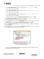
1
Vivado Design Suite Tutorial
Programming and Debugging
UG936 (v2015.1) May 18, 2015
Revision History
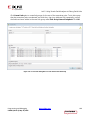
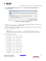
The following table shows the revision history for this document.
Date
Version
Changes
05/18/2015
2015.1
Updates to the tutorials to reflect the 2015.1 Vivado software changes.
Programming and Debugging
UG936 (v2015.1) May 18, 2015
www.xilinx.com
2
Send Feedback
Table of Contents
Revision History ......................................................................................................................................................2
Debugging in Vivado Tutorial .....................................................................................................................................5
Introduction ............................................................................................................................................................5
Objectives ...............................................................................................................................................................5
Getting Started .......................................................................................................................................................6
Lab 1: Using the Netlist Insertion Method for Debugging a Design ........................................................................ 11
Introduction ......................................................................................................................................................... 11
Step 1: Creating a Project with the Vivado New Project Wizard ......................................................................... 11
Step 2: Synthesizing the Design ........................................................................................................................... 12
Step 3: Probing and Adding Debug IP .................................................................................................................. 14
Step 4: Implementing and Generating Bitstream................................................................................................ 24
Lab 2: Using the HDL Instantiation Method for Debugging a Design in Vivado ...................................................... 25
Introduction ......................................................................................................................................................... 25
Step 1: Creating a Project with the Vivado New Project Wizard ......................................................................... 25
Step 2: Synthesize Implement and Generate Bitstream ..................................................................................... 27
Lab 3: Using a VIO Core for Debugging a Design in Vivado ..................................................................................... 29
Introduction ......................................................................................................................................................... 29
Step 1: Creating a Project with the Vivado New Project Wizard ......................................................................... 30
Step 2: Synthesize, Implement, and Generate Bitstream ................................................................................... 35
Lab 4: Using Synplify Pro Synthesis Tool and Vivado for Debugging a Design ........................................................ 36
Introduction ......................................................................................................................................................... 36
Step 1: Create a Synplify Pro Project ................................................................................................................... 36
Step 2: Synthesize the Synplify Project ............................................................................................................... 43
Step 3: Create EDIF Netlists for the Black Box Created in Synplify Pro ............................................................... 44
Step 4: Create a Post Synthesis Project in Vivado IDE ......................................................................................... 46
Step 5: Add (more) Debug Nets to the Project.................................................................................................... 48
Step 6: Implementing the Design and Generating the Bitstream ....................................................................... 50
Using Vivado Logic Analyzer to Debug Hardware ................................................................................................... 51
Introduction ......................................................................................................................................................... 51
Step 1: Verifying Operation of the Sine Wave Generator ................................................................................... 51
Step 2: Debugging the Sine Wave Sequencer State Machine (Optional) ............................................................ 62
Programming and Debugging
UG936 (v2015.1) May 18, 2015
www.xilinx.com
3
Send Feedback
Verifying the VIO Core Activity (Only applicable to Lab 3) .................................................................................. 67
Lab 5: Using Vivado Serial Analyzer to Debug Serial Links ...................................................................................... 79
Introduction ......................................................................................................................................................... 79
Design Description ............................................................................................................................................... 79
Step 1: Creating, Customizing, and Generating an IBERT Design ........................................................................ 80
Step 2: Adding an IBERT core to the Vivado Project ........................................................................................... 81
Step 3: Synthesize, Implement and Generate Bitstream for the IBERT design ................................................... 88
Step 4: Interact with the IBERT core using Serial I/O Analyzer ........................................................................... 90
Lab 6: Using Vivado ILA core to Debug JTAG-AXI Transactions ............................................................................. 107
Introduction ....................................................................................................................................................... 107
Design Description ............................................................................................................................................. 108
Step 1: Opening the JTAG to AXI Master IP Example Design and Configuring the AXI Interface Debug
Connections ....................................................................................................................................................... 108
Step 2: Program the KC705 Board and Interact with the JTAG to AXI Master Core ......................................... 126
Step 3: Using ILA Advanced Trigger Feature to Trigger on an AXI Read Transaction ........................................ 133
Legal Notices.......................................................................................................................................................... 139
Please Read: Important Legal Notices ............................................................................................................... 139
Programming and Debugging
UG936 (v2015.1) May 18, 2015
www.xilinx.com
4
Send Feedback
Debugging in Vivado Tutorial
Introduction
This document contains a set of tutorials designed to help you debug complex FPGA designs. The first
four labs explain different kinds of debug flows that you can chose to use during the course of debug.
These labs introduce the Vivado® debug methodology recommended to debug your FPGA designs.
The labs describe the steps involved in taking a small RTL design and the multiple ways of inserting the
Integrated Logic Analyzer (ILA) core to help debug the design. The fifth lab is for debugging high-speed
serial I/O links in Vivado. The sixth lab is for debugging JTAG-AXI transactions in Vivado. The first four
labs converge at the same point when connected to a target hardware board.
Example RTL designs are used to illustrate overall integration flows between Vivado logic analyzer, ILA,
and Vivado Integrated Design Environment (IDE). In order to be successful using this tutorial, you
should have some basic knowledge of Vivado Design Suite tool flow.
TRAINING: Xilinx provides training courses that can help you learn more about the
concepts presented in this document. Use these links to explore related courses:
Vivado Design Suite Hands-on Introductory Workshop Training Course
Vivado Design Suite Tool Flow Training Course
Essentials of FPGA Design Training Course
Vivado Design Suite User Guide: Programming and Debugging, (UG908).
Objectives
These tutorials:
Show you how to take advantage of integrated Vivado logic analyzer features in the Vivado design
environment that make the debug process faster and simpler.
Provide specifics on how to use the Vivado IDE and the Vivado logic analyzer to debug common
problems in FPGA logic designs.
Provide specifics on how to use the Vivado Serial I/O Analyzer to debug high-speed serial links.
Programming and Debugging
UG936 (v2015.1) May 18, 2015
www.xilinx.com
5
Send Feedback
Debugging in Vivado Tutorial
After completing this tutorial, you will be able to:
Validate and debug your design using the Vivado Integrated Design Environment (IDE) and the
Integrated Logic Analyzer (ILA) core.
Understand how to create an RTL project, probe your design, insert an ILA core, and implement the
design in the Vivado IDE.
Generate and customize an IP core netlist in the Vivado IDE.
Debug the design using Vivado logic analyzer in real-time, and iterate the design using the Vivado
IDE and a KC705 Evaluation Kit Base Board that incorporates a Kintex®-7 device.
Analyze high-speed serial links using the Serial I/O Analyzer.
Getting Started
Setup Requirements
Before you start this tutorial, make sure you have and understand the hardware and software
components needed to perform the labs included in this tutorial as listed below.
Software
Vivado Design Suite 2015.1
Hardware
Kintex-7 FPGA KC705 Evaluation Kit Base Board
Digilent Cable
Two SMA (Sub-miniature version A) cables
Programming and Debugging
UG936 (v2015.1) May 18, 2015
www.xilinx.com
6
Send Feedback
Debugging in Vivado Tutorial
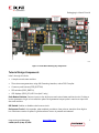
Figure 1: KC705 Board Showing Key Components
Tutorial Design Components
Labs 1 through 4 include:
A simple control state machine
Three sine wave generators using AXI-Streaming interface, native DDS Compiler
Common push buttons (GPIO_BUTTON)
DIP switches (GPIO_SWITCH)
LED displays (GPIO_LED) VIO Core (Lab 3 only)
Push Button Switches: Serve as inputs to the de-bounce and control state machine circuits. Pushing a
button generates a high-to-low transition pulse. Each generated output pulse is used as an input into
the state machine.
DIP Switch: Enables or disables a de-bounce circuit.
De-bounce Circuit: In this example, when enabled, provides a clean pulse or transition from high to
low. Eliminates a series of spikes or glitches when a button is pressed and released.
Programming and Debugging
UG936 (v2015.1) May 18, 2015
www.xilinx.com
7
Send Feedback
Debugging in Vivado Tutorial
Sine Wave Sequencer State Machine: Captures and decodes input from the two push buttons.
Provides sine wave selection and indicator circuits, sequencing among 00, 01, 10, and 11 (zero to three).
LED Displays: GPIO_LED_0 and GPIO_LED_1 display selection status from the state machine outputs,
each of which represents a different sine wave frequency: high, medium, and low.
Lab5 includes:
An IBERT core
A top-level wrapper that instantiates the IBERT core.
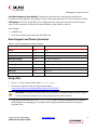
Board Support and Pinout Information
Table 1: Pinout Information for the KC705 Board
Pin Name
Pin Location
Description
CLK_N
AD11
Clock
CLK_P
AD12
Clock
GPIO_BUTTONS[0]
AA12
Reset
GPIO_BUTTONS[1]
AG5
Sine Wave Sequencer
GPIO_SWITCH
Y28
De-bounce Circuit Selector
LEDS_n[0]
AB8
Sine Wave Selection[0]
LEDS_n[1]
AA8
Sine Wave Selection[1]
LEDS_n[2]
AC9
Reserved
LEDS_n[3]
AB9
Reserved
Design Files
1. In your C: drive, create a folder called /Vivado_Debug.
2. Find the tutorial source files at the following location:
https://secure.xilinx.com/webreg/clickthrough.do?cid=385007
CAUTION! The tutorial and design files may be updated or modified between software releases.
You can download the latest version of the material from the Xilinx website.
3. Unzip the tutorial source file to the /Vivado_Debug folder. There are five labs that use different
methodologies for debugging your design. Select the appropriate lab and follow the steps to
complete them
Programming and Debugging
UG936 (v2015.1) May 18, 2015
www.xilinx.com
8
Send Feedback
Debugging in Vivado Tutorial
Lab 1: This lab walks you through the steps of marking nets for debug in HDL as well as the postsynthesis netlist (Netlist Insertion Method). Following are the required files:
debounce.vhd
fsm.vhd
sinegen.vhd
sinegen_demo.vhd
sine_high/sine_high.xci
sine_low/sine_low.xci
sine_mid/sine_mid.xci
sinegen_demo_kc705.xdc
Lab 2: This lab goes over the details of marking nets for debug in the source HDL (HDL instantiation
method) as well as instantiating an ILA core in the HDL. Following are the required files:
debounce.vhd
fsm.vhd
sinegen.vhd
sinegen_demo_inst.vhd
ila_0/ila_0.xci
sine_high/sine_high.xci
sine_low/sine_low.xci
sine_mid/sine_mid.xci
sinegen_demo_kc705.xdc
Lab 3: You can test your design even if the hardware is not physically accessible, using a VIO core. This
lab walks you through the steps of instantiating and customizing a VIO core that you will hook to the
I/Os of the design. Following are the required files:
debounce.vhd
fsm.vhd
sinegen.vhd
sinegen_demo_inst_vio.vhd
sine_high/sine_high.xci
sine_low/sine_low.xci
sine_mid/sine_mid.xci
Programming and Debugging
UG936 (v2015.1) May 18, 2015
www.xilinx.com
9
Send Feedback
Debugging in Vivado Tutorial
ila_0/ila_0.xci
sinegen_demo_kc705.xdc
Lab 4: Nets can also be marked for debug in a third-party synthesis tool using directives for the
synthesis tool. This lab walks you through the steps of marking nets for debug in the Synplify tool and
then using Vivado to perform the rest of the debug. Following are the required files:
dds_compiler_v6_0_viv.edn
dds_compiler_v6_0_viv_parameterized1.edn
dds_compiler_v6_0_viv_parameterized3.edn
debounce.vhd
fsm.vhd
sine_high.xci
sine_low.xci
sine_mid.xci
sinegen.edn
sinegen_synplify.vhd
synplify_1.sdc
sinegen_demo_kc705.xdc
Lab 5: Debug high-speed serial I/O links using the Vivado Serial I/O Analyzer. This lab uses the Vivado
IP example design.
Lab 6: Using Vivado ILA core to debug JTAG-to-AXI transactions. This lab uses the Vivado IP example
design.
Connecting the Boards and Cables
1. Connect the Digilent cable from the Digilent cable connector to a USB port on your computer.
2. Connect the two SMA cables (for lab 5 only) as follows:
a. Connect one SMA cable from J19 (TXP) to J17 (RXP).
b. Connect the other SMA cable from J20 (TXN) to J66 (RXN).
The relative locations of SMA cables on the board are shown in Figure 1: KC705 Board Showing Key
Components.
Programming and Debugging
UG936 (v2015.1) May 18, 2015
www.xilinx.com
10
Send Feedback
Lab 1: Using the Netlist Insertion Method for
Debugging a Design
Introduction
In this lab, you will mark signals for debug in the source HDL as well as the post synthesis netlist. Then
you will create an ILA core and take the design through implementation. Finally, you will use Vivado®
to connect to the KC705 target board and debug your design using Vivado Integrated Logic Analyzer.
Step 1: Creating a Project with the Vivado New Project
Wizard
To create a project, use the New Project wizard to name the project, to add RTL source files and
constraints, and to specify the target device.
1. Invoke the Vivado IDE.
2. In the Getting Started screen, click Create New Project to start the New Project wizard. Click Next.
3. In the Project Name screen, name the new project proj_netlist and provide the project location
(C:/Vivado_Debug). Ensure that Create Project Subdirectory is selected and click Next.
4. In the Project Type screen, specify the Type of Project to create as RTL Project. Click Next.
5. In the Add Sources screen:
a. Set Target Language to VHDL.
b. Click the Add Files button.
c. In the Add Source Files dialog box, navigate to the /src/Lab1 directory.
d. Select all VHD source files, and click OK.
e. Verify that the files are added, and Copy Sources into Project is selected. Click Next.
Programming and Debugging
UG936 (v2015.1) May 18, 2015
www.xilinx.com
11
Send Feedback
Lab 1: Using the Netlist Insertion Method for Debugging a Design
7. In the Add Existing IP (optional) dialog box:
a. Click the Add Files button.
b. In the Add Configurable IP dialog box, navigate to the /src/lab1/sine_high directory.
c. Select XCI source file, and click OK.
d. In the Add Configurable IP dialog box, navigate to the /src/lab1/sine_mid directory.
e. Select XCI source file, and click OK.
f.
In the Add Configurable IP dialog box, navigate to the /src/lab1/sine_low directory.
g. Select XCI source file, and click OK.
h. Verify that the files are added and Copy Sources into Project is selected. Click Next.
8. In the Add Constraints (optional) dialog box, the provided XDC file, sinegen_demo_kc705.xdc,
should automatically appear in the main window. Click Next.
9. In the Default Part dialog box, specify the xc7k325tffg900-2 part for the KC705 platform. You can
also select Boards and then select Kintex-7 KC705 Evaluation Platform. Click Next.
10. Review the New Project Summary page. Verify that the data appears as expected, per the steps
above, and click Finish.
Note: It could take a moment for the project to initialize.
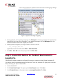
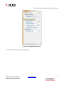
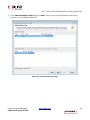
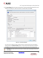
Step 2: Synthesizing the Design
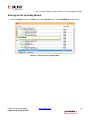
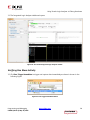
1. In the Project Manager, click Project Settings as shown in the following figure.
Programming and Debugging
UG936 (v2015.1) May 18, 2015
www.xilinx.com
12
Send Feedback
Lab 1: Using the Netlist Insertion Method for Debugging a Design
Figure 2: Configuring the Project Settings
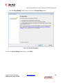
IMPORTANT: As an optional step, in the Project Settings dialog box, select Synthesis from the
left and change flatten hierarchy to none. The reason for changing this setting to none is to
prevent the synthesis tool from performing any boundary optimizations for this tutorial.
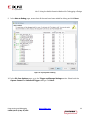
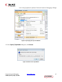
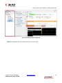
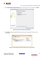
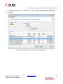
2. In the Vivado Flow Navigator, expand the Synthesis drop-down list, and click Run Synthesis.
Note: When synthesis runs, a progress indicator appears, showing that synthesis is occurring. This
could take a few minutes.
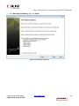
3. In the Synthesis Completed dialog box, click Cancel as shown in the following figure. You will
implement the design later.
Programming and Debugging
UG936 (v2015.1) May 18, 2015
www.xilinx.com
13
Send Feedback
Lab 1: Using the Netlist Insertion Method for Debugging a Design
Figure 3: Synthesis Completed Dialog Box
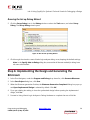
Step 3: Probing and Adding Debug IP
To add a Vivado ILA core to the design, take advantage of the integrated flows between the Vivado IDE
and Vivado logic analyzer.
In this step, you will accomplish the following tasks:
Add debug nets to the project.
Run the Set Up Debug wizard.
Implement and open the design.
Generate the bitstream.
Adding Debug Nets to the Project
Following are some ways to add debug nets using the Vivado IDE:
Add mark_debug attribute to HDL files.
VHDL
attribute
attribute
attribute
attribute
mark_debug : string;
keep : string;
mark_debug of sine
mark_debug of sineSel
: signal is "true";
: signal is "true";
Verilog
(* mark_debug = "true" *) wire sine;
(* mark_debug = "true" *) wire sineSel;
Programming and Debugging
UG936 (v2015.1) May 18, 2015
www.xilinx.com
14
Send Feedback
Lab 1: Using the Netlist Insertion Method for Debugging a Design
This method provides lets you probe signals at the HDL design level. This can prevent optimization
that might have otherwise occurred to that signal. It also lets you pick up the signal tagged for post
synthesis, so you can insert these signals into a debug core and observe the values on this signal
during FPGA operation. This method gives you the highest probability to preserve HDL signal
names after synthesis.
Right-click and select Mark Debug or Unmark Debug on a synthesized netlist.
This method is flexible since it allows probing the synthesized netlist in the Vivado IDE and allowing
you to add/remove MARK_DEBUG attribute at any hierarchy in the design. In addition this method
doesn’t require HDL source modification. However there may be situations where synthesis may not
preserve the signals due to netlist optimization involving absorption or merging of design
structures.
Use a Tcl prompt to set the mark_debug attribute on a synthesized netlist.
set_property mark_debug true [get_nets –hier [list {sine[*]}]]
This applies the MARK_DEBUG on the current, open netlist.
This method is flexible since you can turn MARK_DEBUG on and off by modifying the Tcl command.
In addition, this method does not require HDL source modification. However, there may be
situations where synthesis does not preserve the signals due to netlist optimization involving
absorption or merging of design structures.
In the following steps, you learn how to add debug nets to HDL files and the synthesized design using
Vivado IDE.
TIP: Before proceeding, make sure that the Flow Navigator on the left panel is enabled.
Use Ctrl-Q to toggle it off and on.
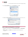
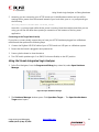
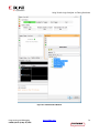
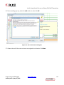
1. In the Flow Navigator under the Synthesis drop-down list, click Open Synthesized Design as
shown in the following figure.
Figure 4: Open Synthesized Design
Programming and Debugging
UG936 (v2015.1) May 18, 2015
www.xilinx.com
15
Send Feedback
Lab 1: Using the Netlist Insertion Method for Debugging a Design
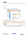
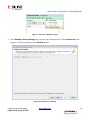
2. In the Window menu, select Layout > Debug. When the Debug window opens. Click the window if
it is not already selected.
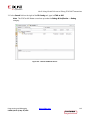
3. Expand Unassigned Debug Nets folder. The following figure shows those debug nets that were
tagged in sinegen_demo.vhd with mark_debug attributes.
Figure 5: VHDL Example Using MARK_DEBUG Attributes
Figure 6: Unassigned Debug Nets Post-Synthesis
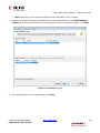
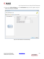
4. Select the Netlist tab and expand Nets. Select the following nets for debugging shown in the
following figure.
o
GPIO_BUTTONS_IBUF[0] and GPIO_BUTTONS_IBUF[1] - Nets folder under the toplevel hierarchy
o
sel(2) - Nets folder under the U_SINEGEN hierarchy
Programming and Debugging
UG936 (v2015.1) May 18, 2015
www.xilinx.com
16
Send Feedback
Lab 1: Using the Netlist Insertion Method for Debugging a Design
o
sine(20)- Nets folder under the U_SINEGEN hierarchy
Figure 7: Add Nets for Debug from the Synthesized Netlist
Note: These signals represent the significant behavior of this design and are used to verify and
debug the design in subsequent steps.
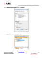
5. Right-click the selected nets and select Mark Debug as shown in the following figure.
Programming and Debugging
UG936 (v2015.1) May 18, 2015
www.xilinx.com
17
Send Feedback
Lab 1: Using the Netlist Insertion Method for Debugging a Design
Figure 8: Adding Nets from the Netlist Tab
6. Next, mark nets for debug in the Tcl console. Mark nets “sine(20)” under the U_SINEGEN
hierarchy for debug by executing the following Tcl command.
set_property mark_debug true [get_nets –hier [list {sine[*]}]]
TIP: In the Debug window, you can see the unassigned nets you just selected. In the Netlist
window, you can also see the green bug icon next to each scalar or bus, which indicates that a
net has the attribute mark_debug = true as shown the following two figures.
Programming and Debugging
UG936 (v2015.1) May 18, 2015
www.xilinx.com
18
Send Feedback
Lab 1: Using the Netlist Insertion Method for Debugging a Design
Figure 9: Newly Added Nets for Debug from the Synthesized Netlist
Figure 10: Netlist View of Nets Marked for Debug
Programming and Debugging
UG936 (v2015.1) May 18, 2015
www.xilinx.com
19
Send Feedback
Lab 1: Using the Netlist Insertion Method for Debugging a Design
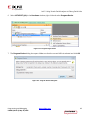
Running the Set Up Debug Wizard
7. From the Debug window or Tools menu, select Set Up Debug. The Set up Debug wizard opens.
Figure 11: Launching the Set up Debug Wizard
Programming and Debugging
UG936 (v2015.1) May 18, 2015
www.xilinx.com
20
Send Feedback
Lab 1: Using the Netlist Insertion Method for Debugging a Design
8. When the Set up Debug wizard opens, click Next.
Figure 12: Set up Debug Wizard
Programming and Debugging
UG936 (v2015.1) May 18, 2015
www.xilinx.com
21
Send Feedback
Lab 1: Using the Netlist Insertion Method for Debugging a Design
9. In the Nets to Debug page, ensure that all the nets have been added for debug and click Next.
Figure 13: Specify Nets to Debug
10. In the ILA Core Options page, go to the Trigger and Storage Settings section. Select both the
Capture Control and Advanced Trigger settings. Click Next.
Programming and Debugging
UG936 (v2015.1) May 18, 2015
www.xilinx.com
22
Send Feedback
Lab 1: Using the Netlist Insertion Method for Debugging a Design
11. In the Setup Debug Summary page, make sure that all the information is correct and as expected.
Click Finish.
Figure 14: Set up Debug Summary
Upon clicking Finish the relevant XDC commands to insert the ILA core(s) are generated.
Programming and Debugging
UG936 (v2015.1) May 18, 2015
www.xilinx.com
23
Send Feedback
Lab 1: Using the Netlist Insertion Method for Debugging a Design
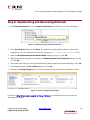
Step 4: Implementing and Generating Bitstream
1. Click Generate Bitstream from the Program and Debug drop-down list in the Flow Navigator.
Figure 15: Implement Design and Generate Bitstream
2. In the Save Project dialog box click Save. This applies the mark_debug attributes on the newly
marked nets. You can see those constraints by inspecting the sinegen_demo_kc705.xdc file.
3. When the No Implementation Results Available dialog box pops up, click Yes.
4. When the bitstream generation completes, the Bitstream Generation Completed dialog box pops
up. Click OK.
5. In the dialog box asking to close synthesized design before opening implemented design. Click Yes.
6. In the Implementation is Out-of-date dialog box, click Yes.
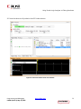
7. Examine the Timing Summary report to ensure that all the specified timing constraints are met.
Figure 16: View the Timing Summary Report
Proceed to
debugging the design.
Programming and Debugging
UG936 (v2015.1) May 18, 2015
to complete the rest of the steps for
www.xilinx.com
24
Send Feedback
Lab 2: Using the HDL Instantiation Method for
Debugging a Design in Vivado
Introduction
The HDL Instantiation method is one of the two methods supported in Vivado® Debug Probing. For
this flow, you will generate an ILA IP using the Vivado IP Catalog and instantiate the core in a design
manually as you would with any other IP.
Step 1: Creating a Project with the Vivado New Project
Wizard
To create a project, use the New Project wizard to name the project, to add RTL source files and
constraints, and to specify the target device.
1. Invoke the Vivado IDE.
2. In the Getting Started page, click Create New Project to start the New Project wizard. Click Next.
3. In the Project Name page, name the new project proj_hdl and provide the project location
(C:/Vivado_Debug). Ensure that Create Project Subdirectory is selected. Click Next.
4. In the Project Type page, specify the Type of Project to create as RTL Project. Click Next.
5. In the Add Sources page:
a. Set Target Language to VHDL.
b. Click Add Files.
c. In the Add Source Files dialog box, navigate to the /src/Lab2 directory.
d. Select all VHD source files, and click OK.
e. Verify that the files are added, and Copy Sources into Project is selected. Click Next.
6. 6. In the Add Existing IP (optional) page:
a. Click Add Files.
b. In the Add Configurable IP dialog box, navigate to the /src/lab1/sine_high directory.
c. Select XCI source file, and click OK.
Programming and Debugging
UG936 (v2015.1) May 18, 2015
www.xilinx.com
25
Send Feedback
Lab 2: Using the HDL Instantiation Method for Debugging a Design in Vivado
d. In the Add Configurable IP dialog box, navigate to the /src/lab1/sine_mid directory.
e. Select XCI source file, and click OK.
f.
In the Add Configurable IP dialog box, navigate to the /src/lab1/sine_low directory.
g. Select XCI source file, and click OK.
h. In the Add Configurable IP dialog box, navigate to the /src/lab1/ila_0 directory.
i.
Select XCI source file, and click OK.
j.
Verify that the files are added, and Copy Sources into Project is selected. Click Next.
7. In the Add Constraints (optional) page, the provided XDC file, sinegen_demo_kc705.xdc
should automatically appear in the main window. Click Next.
8. In the Default Part page, specify the xc7k325tffg900-2 part for the KC705 platform. You can also
select Boards and then select Kintex-7 KC705 Evaluation Platform. Click Next.
9. Review the New Project Summary page. Verify that the data appears as expected, per the steps
above. Click Finish.
10. In the Sources window in Vivado IDE, expand sinegen_demo_inst to see the source files for this
lab. Note that ila_0 core has been added to the project.
Figure 17: ILA Instantiation in HDL
Double-click the sinegen_demo_inst.vhd file to open it and inspect the instantiation and port
mapping of the ILA core in the HDL code.
Programming and Debugging
UG936 (v2015.1) May 18, 2015
www.xilinx.com
26
Send Feedback
Lab 2: Using the HDL Instantiation Method for Debugging a Design in Vivado
Figure 18: Hook Signals that Requiring Debugging in the ILA
Step 2: Synthesize Implement and Generate Bitstream
1. From the Program and Debug drop-down list, in Flow Navigator, click Generate Bitstream. This
will synthesize, implement and generate a bitstream for the design.
Figure 19: Generate Bitstream
2. The No Implementation Results Available dialog box appears. Click Yes.
3. After bitstream generation completes, the Bitstream Generation Completed dialog box appears.
Open Implemented Design is selected by default. Click OK.
4. In the Report Timing Summary dialog box. Make sure that all timing constraints are met. Click OK.
Programming and Debugging
UG936 (v2015.1) May 18, 2015
www.xilinx.com
27
Send Feedback
Lab 2: Using the HDL Instantiation Method for Debugging a Design in Vivado
Figure 20: Review Timing Summary
5. Proceed to Using Vivado Logic Analyzer to Debug Hardware chapter to complete the rest of this lab.
Programming and Debugging
UG936 (v2015.1) May 18, 2015
www.xilinx.com
28
Send Feedback
Lab 3: Using a VIO Core for Debugging a Design in
Vivado
Introduction
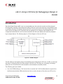
The Virtual Input/Output (VIO) core is a customizable core that can both monitor and drive internal
FPGA signals in real time. The number and width of the input and output ports are customizable in size
to interface with the FPGA design. Because the VIO core is synchronous to the design being monitored
and/or driven, all design clock constraints that are applied to your design are also applied to the
components inside the VIO core. Run time interaction with this core requires the use of the Vivado®
logic analyzer feature. The following figure is a block diagram of the new VIO core.
Figure 21: VIO Block Diagram
This lab walks you through the steps of instantiating and configuring the VIO core. It walks you through
the steps of connecting the I/Os of the design to the VIO core. This way, you can debug your design
when you do not have access to the hardware or the hardware is remotely located.
The following ports are created:
One 4-bit PROBE_IN0 port. This has two bits to monitor the 2-bit Sine Wave selector outputs from
the finite state machine (FSM) and other two bits to mimic the state of the other two LEDs on the
Programming and Debugging
UG936 (v2015.1) May 18, 2015
www.xilinx.com
29
Send Feedback
Lab 3: Using a VIO Core for Debugging a Design in Vivado
board. We will configure these 4-bit signals as LEDs during run time to mimic the LEDs displayed on
the KC705 board.
One 2-bit PROBE_OUT0 port to drive the input buttons on the FSM. We will configure it so one bit
can be used as a toggle switch during run time to mimic the “PUSH_BUTTON”, SW3, and second bit
will be used as the “PUSH_BUTTON”, SW6.
Step 1: Creating a Project with the Vivado New Project
Wizard
To create a project, use the New Project wizard to name the project, to add RTL source files and
constraints, and to specify the target device.
1. Invoke Vivado IDE.
2. In the Getting Started page, click Create New Project to start the New Project wizard. Click Next.
3. In the Project Name page, name the new project proj_hdl_vio and provide the project location
(C:/Vivado_Debug). Ensure that Create project subdirectory is selected. Click Next.
4. In the Project Type page, specify the Type of Project to create as RTL Project. Click Next.
5. In the Add Sources page:
a. Set Target Language to VHDL.
b. Click Add Files.
c. In the Add Source Files dialog box, navigate to the /src/Lab3 directory.
d. Select all VHD source files, and click OK.
e. Verify that the files are added, and Copy Sources into Project is selected. Click Next.
6. In the Add Existing IP (optional) page:
a. Click the Add Files.
b. In the Add Configurable IP dialog box, navigate to the /src/lab1/sine_high directory.
c. Select all XCI source files, and click OK.
d. In the Add Configurable IP dialog box, navigate to the /src/lab1/sine_mid directory.
e. Select all XCI source files, and click OK.
f.
In the Add Configurable IP dialog box, navigate to the /src/lab1/sine_low directory.
g. Select all XCI source files, and click OK.
h. In the Add Configurable IP dialog box, navigate to the /src/lab1/ila_0 directory.
Programming and Debugging
UG936 (v2015.1) May 18, 2015
www.xilinx.com
30
Send Feedback
Lab 3: Using a VIO Core for Debugging a Design in Vivado
i.
Select all XCI source files, and click OK.
j.
Verify that the files are added and Copy sources into project is selected. Click Next.
7. In the Add Constraints (optional) dialog box, the provided XDC file, sinegen_demo_kc705.xdc,
should automatically appear in the main window. Click Next.
8. In the Default Part page, specify the xc7k325tffg900-2 part for the KC705 platform. You can also
select Boards and then select Kintex-7 KC705 Evaluation Platform. Click Next.
9. Review the New Project Summary page. Verify that the data appears as expected, per the steps
above. Click Finish.
Note: It might take a moment for the project to initialize.
10. In the Sources window in Vivado IDE, expand sinegen_demo_inst_vio to see the source files for this
lab. Note that ila_0 core has been added to the project. However, vio_0 (the VIO core) is
missing.
Figure 22: Missing Source for VIO Core
In the following step, you will instantiate and configure this VIO core.
11. From the Flow Navigator, click IP Catalog, expand Debug & Verification, then expand Debug,
and double-click VIO. The Customize IP dialog box opens.
12. On the General Options tab, leave the Component Name to its default value of vio_0, set Input
Probe Count to 1, Output Probe Count to 1, and select the Enable Input Probe Activity
Detectors check box.
Programming and Debugging
UG936 (v2015.1) May 18, 2015
www.xilinx.com
31
Send Feedback
Lab 3: Using a VIO Core for Debugging a Design in Vivado
Figure 23: Configure General Options of the VIO Core
13. On the PROBE_IN Ports tab, set Probe Width to 4 bits wide.
Figure 24: Configure PROBE_IN Ports of the VIO Core
Programming and Debugging
UG936 (v2015.1) May 18, 2015
www.xilinx.com
32
Send Feedback
Lab 3: Using a VIO Core for Debugging a Design in Vivado
14. On the PROBE _OUT Ports, set Probe Width to 2 bits wide with an initial value of 0 in hex format.
Figure 25: Configure the PROBE_OUT Ports of the VIO Core
15. Click OK to generate the IP. The Generate Output Products dialog box will appear. Click Generate.
Figure 26: Generate Output Products for the VIO Core
Programming and Debugging
UG936 (v2015.1) May 18, 2015
www.xilinx.com
33
Send Feedback
Lab 3: Using a VIO Core for Debugging a Design in Vivado
Output product generation should take less than a minute. At this point, you have finished
customizing the VIO. This core has already been instantiated in the top level design as shown in the
following figure.
Figure 27: VIO Instantiation in the Top Level Design
At this point, the Sources window should look as shown in the following figure.
Figure 28: Instantiated VIO Core in the Sources Window
Programming and Debugging
UG936 (v2015.1) May 18, 2015
www.xilinx.com
34
Send Feedback
Lab 3: Using a VIO Core for Debugging a Design in Vivado
16. Double-click sinegen_demo_inst.vhd in the Sources window, to open it and inspect the
instantiation and port mapping of the ILA core in the HDL code.
Figure 29: Hook signals that need to be debugged in the ILA
Step 2: Synthesize, Implement, and Generate Bitstream
1. From the Program and Debug drop-down list, in Flow Navigator, click Generate Bitstream. This
synthesizes, implements, and generates a bitstream for the design.
2. The No Implementation Results Available dialog box appears. Click Yes.
3. After bitstream generation completes, the Bitstream Generation Completed dialog box appears.
Open Implemented Design is selected by default. Click OK.
4. Inspect the Timing Summary report and make sure that all timing constraints have been met.
Figure 30: Report Timing Summary Dialog Box
5. Proceed to Using Vivado Logic Analyzer to Debug Hardware. chapter to complete the rest of the
steps for debugging the design. Skip forward to Verifying the VIO Core Activity (Only applicable
to Lab 3) section to complete the rest of this lab.
Programming and Debugging
UG936 (v2015.1) May 18, 2015
www.xilinx.com
35
Send Feedback
Lab 4: Using Synplify Pro Synthesis Tool and Vivado
for Debugging a Design
Introduction
This simple tutorial shows how to do the following:
Create a Synplify Pro project for the wave generator design.
Mark nets for debug in the Synplify Pro constraints file as well as VHDL source files.
Synthesize the Synplify Pro project to create an EDIF netlist.
Create a Vivado® project based on the Synplify Pro netlist.
Use the Vivado IDE to setup and debug the design from the synthesized design using Synplify Pro
(Version 2013-3 SP1).
Step 1: Create a Synplify Pro Project
1. Launch Synplify Pro and select File > New. Set File Type to Project File (Project) as highlighted in
the following figure. In the New File Name box, enter synplify_1. Click OK.
Figure 31: Synplify Pro New Project Dialog Box
Programming and Debugging
UG936 (v2015.1) May 18, 2015
www.xilinx.com
36
Send Feedback
Lab 4: Using Synplify Pro Synthesis Tool and Vivado for Debugging a Design
2. If you get a dialog box asking you to create a non-existing directory click OK.
Figure 32: Synplify Pro project Confirmation Dialog Box
3. In the left panel of the Synplify Pro window, click Add File as shown in the following figure.
Figure 33: Adding Files to a Synplify Pro Project
4. In the Add Files to Project dialog box, change the Files of Type to HDL File. Navigate to
C:\Vivado_Debug\src\Lab4, which shows all the VHDL source files needed for this lab. Select
the following three files by pressing the Ctrl key and clicking on them.
debounce.vhd
fsm.vhd
sinegen_demo.vhd
Click Add.
Programming and Debugging
UG936 (v2015.1) May 18, 2015
www.xilinx.com
37
Send Feedback
Lab 4: Using Synplify Pro Synthesis Tool and Vivado for Debugging a Design
Figure 34: Adding VHDL Source Files to the Synplify Pro Project
Programming and Debugging
UG936 (v2015.1) May 18, 2015
www.xilinx.com
38
Send Feedback
Lab 4: Using Synplify Pro Synthesis Tool and Vivado for Debugging a Design
6. In the same dialog box set Files of type to Constraints File. This shows the synplify_1.sdc file.
Select the file and click Add as shown in the following figure.
Figure 35: Adding SDC Constraints File to the Synplify Pro Project
Programming and Debugging
UG936 (v2015.1) May 18, 2015
www.xilinx.com
39
Send Feedback
Lab 4: Using Synplify Pro Synthesis Tool and Vivado for Debugging a Design
7. In the same dialog box set Files of type to Compiler Directives File. This shows the
synplify_1.cdc file. Select the file and click Add as shown in the following figure. Click OK.
Figure 36: Adding CDC Constraints File to the Synplify Pro Project
Programming and Debugging
UG936 (v2015.1) May 18, 2015
www.xilinx.com
40
Send Feedback
Lab 4: Using Synplify Pro Synthesis Tool and Vivado for Debugging a Design
8. Now, you need to set the implementation options. Click Implementation Options in the Synplify
Pro window as shown in the following figure.
Figure 37: Opening Implementation Options in Synplify Pro
9. This brings up the Implementation Options dialog box as shown in the following figure. In the
Device tab, set Technology to Xilinx Kintex7, Part to XC7K325T, Package to FFG900 and Speed
to -2. Leave all the other options at their default values. Click OK.
Programming and Debugging
UG936 (v2015.1) May 18, 2015
www.xilinx.com
41
Send Feedback
Lab 4: Using Synplify Pro Synthesis Tool and Vivado for Debugging a Design
Figure 38: Specifying Implementation Options in Synplify Pro
10. You need to preserve the net names that you want to debug by putting attributes in the HDL files.
These attributes are already placed in the sinegen_demo.vhd, file of this tutorial. Open the
sinegen_demo.vhd file and inspect the lines shown.
Figure 39: Specifying Attributes to Preserve Net Names in Synplify
11. You also can specify the mark_debug attributes in the source HDL files to mark the signals for
debug, as shown in the snippet code from singen_demo.vhd file.
Figure 40: Add Mark_Debug Attribute in HDL File
Programming and Debugging
UG936 (v2015.1) May 18, 2015
www.xilinx.com
42
Send Feedback
Lab 4: Using Synplify Pro Synthesis Tool and Vivado for Debugging a Design
12. The synplify_1.sdc file contains various kinds of constraints such as pin location, I/O standard,
and clock definition. The synplify_1.cdc file contains directives for the compiler. Here is where
the nets of interest to us that are marked for debug are located. The attribute and the nets selected
for debug are shown in the following figure.
Figure 41: Synplify Pro Constraints in CDC Files
In the above constraints, sinegen has been defined as a black box by using the syn_black_box
attribute. Second, the syn_no_prune attribute has been used so that the I/Os of this block are not
optimized away. Finally, two nets, sine[20:0] and sel[1:0] have been assigned the
mark_debug attribute such that these two nets should show up in the synthesized design in Vivado
IDE for further debugging. For further information on these attributes, please refer to the Synplify
Pro User Manual and Synplify Pro Reference Manual.
Step 2: Synthesize the Synplify Project
1. Before implementing the project, you need to set the name for the output netlist file. By default, the
name of the output netlist file is synplify_1.edf. To change the name of the output file, type the
following command at the Tcl command prompt:
%project -result_file "./rev_1/sinegen_demo.edf"
You will use this file in Vivado IDE.
2. With all the project settings in place, click the Run button in the left panel of the Synplify Pro
window to start synthesizing the design.
Programming and Debugging
UG936 (v2015.1) May 18, 2015
www.xilinx.com
43
Send Feedback
Lab 4: Using Synplify Pro Synthesis Tool and Vivado for Debugging a Design
Figure 42: Synthesize the Design in Synplify
3. During synthesis, status messages appear in the Tcl Script tab. Warning messages are expected, but
there should not be any Error messages. To see detailed messages, click the Messages tab in the
bottom left-hand corner of the Synplify Pro console.
4. When synthesis completes, the output netlist is written to the file:
rev_1/sinegen_demo.edf
[Optional] To view the netlist select View > View Result File.
5. Click File > Save All to save the project, then click File > Exit.
Step 3: Create EDIF Netlists for the Black Box Created in
Synplify Pro
The black box, sinegen, created in the Synplify Pro project, contains the Direct Digital Synthesizer IP.
You need to create a synthesized design for this block. To do this, create an RTL type project in Vivado
IDE by following the steps outlined below.
1. Launch Vivado IDE.
2. Click Create New Project. This opens up the New Project wizard. Click Next.
3. Under Project Name, set the project name to proj_synplify_netlist. Click Next.
Programming and Debugging
UG936 (v2015.1) May 18, 2015
www.xilinx.com
44
Send Feedback
Lab 4: Using Synplify Pro Synthesis Tool and Vivado for Debugging a Design
4. Under Project Type, select RTL Project. Click Next.
5. Under Add Sources, click Add Files, navigate to the Vivado_Debug/src/Lab4 folder and select
the sinegen.vhd file. Set Target Language to VHDL. Ensure that Copy sources into project box
is selected. Click Next.
6. Under Add Existing IP, click Add Files, navigate to the Vivado_Debug/src/Lab4 folder and
select the sine_high.xci, sine_low.xci, and sine_mid.xci files. Click Next.
7. Under Add Constraints, the .sdc files are automatically added to the project. These files are not
needed for this step. Remove them from this project by clicking Remove Selected File on the right
of the dialog box. Click Next.
8. Under Default Part, select Boards and then select the Kintex-7 KC705 Evaluation Platform and
correct version for your hardware. Click Next.
9. Under New Project Summary, ensure that all the settings are correct. Click Finish.
10. Once the project has been created, in Vivado Flow Navigator, under the Project Manager folder,
click Project Settings. In the pop-up dialog box, in the left panel, click Synthesis. From the pull
down menu on the right panel, set -flatten_hierarchy to none. Click OK.
11. In Vivado IDE Flow Navigator, under Synthesis Folder, click Run Synthesis.
12. When synthesis completes the Synthesis Completed dialog box appears. Select Open Synthesized
Design and click OK.
13. Now you need to write the netlist file for all the components used in the sinegen block. The four
netlist files used in this tutorial are already provided as a part of the source files. However, you can
overwrite them by using your own netlist files. To do this use the following Tcl command in the Tcl
console of Vivado IDE.
write_edif
-force ../Vivado_Debug/src/Lab4/sinegen.edn
Ensure that the path specified to the src folder is correct. At this point, you should see four .edn
files in the Vivado_Debug/src folder as shown below:
o
dds_compiler_v6_0_viv.edn
o
dds_compiler_v6_0_viv_parameterized1.edn
o
dds_compiler_v6_0_viv_parameterized3.edn
o
sinegen.edn
14. Click File > Exit in Vivado IDE. When the OK to exit dialog box pops up, click OK.
Programming and Debugging
UG936 (v2015.1) May 18, 2015
www.xilinx.com
45
Send Feedback
Lab 4: Using Synplify Pro Synthesis Tool and Vivado for Debugging a Design
Step 4: Create a Post Synthesis Project in Vivado IDE
1. Launch Vivado IDE.
2. Click Create New Project. This opens up the New Project wizard. Click Next.
3. Set the Project Name to proj_synplify. Click Next.
4. Under Project Type, select Post-synthesis Project. Click Next.
5. Under Add Netlist Sources, click Add Files, navigate to the Vivado_Debug/synopsys/rev_1
folder, and select sinegen_demo.edf. Click OK.
6. Add the four netlist files created in the previous section. Click Add Files again, navigate to the
Vivado_Debug/src/Lab4 folder and select the following files:
sinegen.edn
dds_compiler_v6_0_viv.edn
dds_compiler_v6_0_viv_parameterized1.edn
dds_compiler_v6_0_viv_parameterized3.edn
Click OK in the Add Source Files dialog box. In the Add Netlist Sources dialog box ensure that
Copy Sources into Project is selected. Click Next.
7. Under Add Constraints, a .sdc file. should be automatically populated. Remove this file by
selecting it and clicking Remove Selected File on the right of the dialog box. Click Add Files ,
navigate to the Vivado_debug/src folder, and select the sinegen_demo_kc705.xdc file. This file
has the appropriate constraints needed for this Vivado project. Click OK in the Add Constraints File
dialog box. In the Add Constraints (optional) dialog box ensure that Copy Constraints into
Project is selected. Click Next.
8. Under Default Part, select Boards and then select Kintex-7 KC705 Evaluation Platform and the
right version number for your hardware. Click Next.
9. Under New Project Summary, ensure that all the settings are correct and click Finish.
10. In the Sources window, select sinegen_demo.edf and select Specify Top Module.
Programming and Debugging
UG936 (v2015.1) May 18, 2015
www.xilinx.com
46
Send Feedback
Lab 4: Using Synplify Pro Synthesis Tool and Vivado for Debugging a Design
Figure 43: Specifying the Top-Level Module
11. In the Specify Top Module dialog box, click Browse.
Figure 44: Browse to the Top Module
Programming and Debugging
UG936 (v2015.1) May 18, 2015
www.xilinx.com
47
Send Feedback
Lab 4: Using Synplify Pro Synthesis Tool and Vivado for Debugging a Design
12. In the Select Top Module dialog box, select sinegen_demo, then click OK.
Figure 45: Select the Top Level Module
13. Click OK in the Specify Top Module dialog box after ensuring that the top level module is correct.
Figure 46: Specify sinegen_demo as the Top Level Module
Step 5: Add (more) Debug Nets to the Project
1. In Vivado IDE, in the Flow Navigator, select Open Synthesized Design from the Netlist Analysis
folder.
2. Select the Netlist tab in the Netlist window to expand Nets. Select the following nets for
debugging:
Programming and Debugging
UG936 (v2015.1) May 18, 2015
www.xilinx.com
48
Send Feedback
Lab 4: Using Synplify Pro Synthesis Tool and Vivado for Debugging a Design
GPIO_BUTTONS_c(2)
sine (20)
sineSel (2)
After selecting all the nets mentioned above click Mark Debug.
Figure 47: Mark Additional Signals for Debug
3. In the Confirm Debug Net(s) dialog box, click OK.
4. You should be able to see all the nets that are marked for debug as shown in the following figure.
Figure 48: Nets Added for Debug through the Synplify Pro Flow in Vivado IDE
Programming and Debugging
UG936 (v2015.1) May 18, 2015
www.xilinx.com
49
Send Feedback
Lab 4: Using Synplify Pro Synthesis Tool and Vivado for Debugging a Design
Running the Set up Debug Wizard
5. Click the Set up Debug icon in the Debug window or select the Tools menu, and select Set up
Debug. The Set up Debug wizard opens.
Figure 49: Run the Set up Debug Wizard
6. Click through the wizard to create Vivado logic analyzer debug cores, keeping the default settings.
Note: In the Specify Nets to Debug dialog box, ensure that all the nets marked for debug have
the same clock domain.
Step 6: Implementing the Design and Generating the
Bitstream
1. In the Flow Navigator, under the Program and Debug drop-down list, click Generate Bitstream.
2. In the Save Project dialog box, click Save.
3. When the Bitstream generation finishes, the Bitstream Generation Completed dialog box pops-up
and Open Implemented Design is selected by default. Click OK.
4. If you get a dialog box asking to close the synthesized design before opening the implemented
design, click Yes.
5. Proceed to Using Vivado Logic Analyzer to Debug Hardware to complete the rest of this lab.
Programming and Debugging
UG936 (v2015.1) May 18, 2015
www.xilinx.com
50
Send Feedback
Using Vivado Logic Analyzer to Debug Hardware
Introduction
The final step in debugging is to connect to the hardware and debug your design using the Integrated
Logic Analyzer. Before continuing, make sure you have the KC705 hardware plugged into a machine.
In this step, you learn:
How to debug the design using the Vivado® logic analyzer.
How to use the currently supported Tcl commands to communicate with your target board (KC705).
How to discover and correct a circuit problem by identifying unintended behaviors of the push
button switch.
Some useful techniques for triggering and capturing design data.
Step 1: Verifying Operation of the Sine Wave Generator
After doing some setup work, you will use Vivado logic analyzer to verify that the sine wave generator is
working correctly. Your two primary objectives are to verify that:
All sine wave selections are correct.
The selection logic works correctly.
Target Board and Server Set Up
Connecting to the target board remotely
If you plan to connect remotely, you will need to make sure you have KC705 hardware plugged into a
machine and you are running an hw_server application on that machine. If you plan to connect locally,
skip steps 1-4 below and go directly to the Connecting to the Target Board Locally section.
1. Connect the Digilent USB JTAG cable of your KC705 board to a USB port on a Windows system.
2. Ensure that the board is plugged in and powered on.
3. Power cycle the board to clear the device.
4. Turn DIP switch positions (pin 1 on SW13, De-bounce Enable) to the OFF position.
Programming and Debugging
UG936 (v2015.1) May 18, 2015
www.xilinx.com
51
Send Feedback
Using Vivado Logic Analyzer to Debug Hardware
5. Assuming you are connecting your KC705 board to a 64-bit Windows machine and you will be
running the hw_server from the network instead of your local drive, open a cmd prompt and type
the following:
<Xilinx_Install>\Vivado\2015.1\bin\hw_server
Leave this cmd prompt open while the hw_server is running. Note the machine name that you are
using, you will use this later when opening a connection to this instance of the hw_server
application.
Connecting to the Target Board Locally
If you plan to connect locally, ensure that you have your KC705 hardware plugged into a Windows
machine and then perform the following steps:
1. Connect the Digilent USB JTAG cable of your KC705 board to a USB port on a Windows system.
2. Ensure that the board is plugged in and powered on.
3. Power cycle the board to clear the device.
4. Turn DIP switch positions (pin 1 on SW13, De-bounce Enable) to the OFF position.
Using the Vivado Integrated Logic Analyzer
1. In the Flow Navigator, from the Program and Debug drop-down list, select Open Hardware
Manager.
Figure 50: Open Hardware Manager
2. The Hardware Manager window opens. Click Open New Target… . The Open New Hardware
Target wizard opens.
Programming and Debugging
UG936 (v2015.1) May 18, 2015
www.xilinx.com
52
Send Feedback
Using Vivado Logic Analyzer to Debug Hardware
Figure 51: Connect to a Hardware Target
3. In the Hardware Server Settings page, type the name of the server (or select Local server if the
target is on the local machine) in the Connect to field.
Figure 52: Hardware Server Settings
Programming and Debugging
UG936 (v2015.1) May 18, 2015
www.xilinx.com
53
Send Feedback
Using Vivado Logic Analyzer to Debug Hardware
Note: Depending on your connection speed, this may take about 10 to 15 seconds.
4. If there is more than one target connected, you will see multiple entries in the Select Hardware
Target page. In this tutorial, there is only one target, as shown in the following figure. Click Next.
Figure 53: Select Hardware Target
5. Leave these settings at their default values. Click Next.
Programming and Debugging
UG936 (v2015.1) May 18, 2015
www.xilinx.com
54
Send Feedback
Using Vivado Logic Analyzer to Debug Hardware
6. In the Open Hardware Target Summary page, click Finish as shown in the following figure.
Figure 54: Hardware Target Summary
7. Wait for the connection to the hardware to complete. The dialog in following figure appears while
hardware is connecting.
Figure 55: Open Hardware Target
After the connection to the hardware target is made, the dialog shown in the following figure
appears.
Note: The Hardware tab in the Debug view shows the hardware target and XC7K325T device
detected in the JTAG chain.
Programming and Debugging
UG936 (v2015.1) May 18, 2015
www.xilinx.com
55
Send Feedback
Using Vivado Logic Analyzer to Debug Hardware
Figure 56: Active Target Hardware
8. Next, program the XC7K325T device using the .bit bitstream file that was created previously by
right-clicking the XC7K325T device and selecting Program Device as shown in the following
figure.
Figure 57: Program Active Target Hardware
Programming and Debugging
UG936 (v2015.1) May 18, 2015
www.xilinx.com
56
Send Feedback
Using Vivado Logic Analyzer to Debug Hardware
9. In the Program Device dialog box verify that the .bit file is correct for the lab that you are
working on and click Program to program the device as shown in the following figure.
Figure 58: Select Bitstream File to Download for Lab 1
CAUTION! The file paths of the bitstream to be programmed will be different for different labs.
Ensure that the relative paths are correct.
Note: Wait for the program device operation to complete. This may take few minutes.
10. Ensure that an ILA core was detected in the Hardware panel of the Debug view.
Figure 59: ILA Core Detection
Programming and Debugging
UG936 (v2015.1) May 18, 2015
www.xilinx.com
57
Send Feedback
Using Vivado Logic Analyzer to Debug Hardware
11. The Integrated Logic Analyzer dashboard opens.
Figure 60: The Vivado Integrated Logic Analyzer window
Verifying Sine Wave Activity
12. Click Run Trigger Immediate to trigger and capture data immediately as shown in shown in the
following figure.
Figure 61: Run Trigger Immediate Button
Programming and Debugging
UG936 (v2015.1) May 18, 2015
www.xilinx.com
58
Send Feedback
Using Vivado Logic Analyzer to Debug Hardware
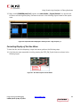
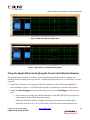
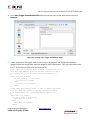
13. In the Waveform window, verify that there is activity on the 20-bit sine signal as shown in the
following figure.
Figure 62: Output Sine Wave Displayed in Digital Format
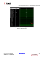
Displaying the Sine Wave
14. Right-click U_SINEGEN/sine[19:0] signals, and select Waveform Style >Analog as shown in the
following figure.
TIP: The waveform does not look like a sine wave. This is because you must change the radix
setting from Hex to Signed Decimal, as described in the following subsection.
Figure 63: Output Sine Wave Displayed in Analog Format - High Frequency 1
Programming and Debugging
UG936 (v2015.1) May 18, 2015
www.xilinx.com
59
Send Feedback
Using Vivado Logic Analyzer to Debug Hardware
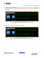
15. Right-click U_SINEGEN/sine[19:0] signals, and select Radix > Signed Decimal. You should now
be able to see the high frequency sine wave as shown in the following figure instead of the square
wave.
Figure 64: Output Sine Wave Displayed in Analog Format - High Frequency 2
Correcting Display of the Sine Wave
To view the mid, and low frequency output sine waves, perform the following steps:
16. Cycle the sine wave sequential circuit by pressing the GPIO_SW_E push button as shown in the
following figure.
Figure 65: Sine Wave Sequencer Push Button
Programming and Debugging
UG936 (v2015.1) May 18, 2015
www.xilinx.com
60
Send Feedback
Using Vivado Logic Analyzer to Debug Hardware
17. Click Run Trigger Immediately again to see the new sine selected sine wave. You should see the
mid frequency as shown in the following figure. Notice that the sel signal also changed from 0 to 1
as expected.
Figure 66: Output Sine Wave Displayed in Analog Format - Mid Frequency
18. Repeat step 17 and 18 to view other sine wave outputs.
Figure 67: Output Sine Wave Displayed in Analog Format - Low Frequency
Programming and Debugging
UG936 (v2015.1) May 18, 2015
www.xilinx.com
61
Send Feedback
Using Vivado Logic Analyzer to Debug Hardware
Figure 68: Output Sine Wave Displayed in Analog Format - Mixed Frequency
Note: As you sequence through the sine wave selections, you may notice that the LEDs do not light
up in the expected order. You will debug this in the next section of this tutorial. For now, verify for
each LED selection, that the correct sine wave displays. Also, note that the signals in the Waveform
window have been re-arranged in the previous three figures.
Step 2: Debugging the Sine Wave Sequencer State Machine
(Optional)
As you were correcting the sine wave display, the LEDs might not have lit up in sequence as you
pressed the Sine Wave Sequencer button. With each push of the button, there should be a single, cyclewide pulse on the GPIO_BUTTONS_re[1] signal. If there is more than one, the behavior of the LEDs
becomes irregular. In this section of the tutorial, use Vivado logic analyzer to probe the sine wave
sequencer state machine, and to view and repair the root cause of the problem.
Before starting the actual debug process, it is important to understand more about the sine wave
sequencer state machine.
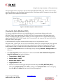
Sine Wave Sequencer State Machine Overview
The sine wave sequencer state machine selects one of the four sine waves to be driven onto the sine
signal at the top-level of the design. The state machine has one input and one output. The following
figure shows the schematic elements of the state machine. Refer to this diagram as you read the
following description and as you perform the steps to view and repair the state machine glitch.
The input is a scalar signal called “button”. When the button input equals “1”, the state machine
advances from one state to the next.
The output is a 2-bit signal vector called “Y”, and it indicates which of the four sine wave generators
is selected.
Programming and Debugging
UG936 (v2015.1) May 18, 2015
www.xilinx.com
62
Send Feedback
Using Vivado Logic Analyzer to Debug Hardware
The input signal button connects to the top-level signal GPIO_BUTTONS_re[1], which is a low-to-high
transition indicator on the Sine Wave Sequencer button. The output signal Y connects to the top-level
signal, sineSel, which selects the sine wave.
Figure 69: Sine Wave Sequencer Button Schematic
Viewing the State Machine Glitch
You cannot troubleshoot the issue you identified above by connecting a debug probe to the
GPIO_BUTTON [1] input signal itself. The GPIO_BUTTON [1] input signal is a PAD signal that is not
directly accessible from the FPGA fabric. Instead, you must trigger on low-to-high transitions (rising
edges) on the GPIO_BUTTON_IBUF signal, which is connected to the output of the input buffer of the
GPIO_BUTTON [1] input signal.
As described earlier, the glitch reveals itself as multiple low-to-high transitions on the
GPIO_BUTTONS_1_IBUF signal, but it occurs intermittently. Because it could take several button presses
to detect it, you will now set up the Vivado logic analyzer tool to Repetitive Trigger Run Mode. This
setting makes it easier to repeat the button presses and look for the event in the Waveform viewer.
1. Open the Debug Probes window if not already open by selecting Window > Debug Probes from
the menu.
2. In the ILA Properties window scroll down to the link marked To view editable ILA Properties:
Open ILA Dashboard and set the following:
a. Trigger Mode to BASIC_ONLY
b. Capture Mode to BASIC
c. Window Data Depth to 1024
d. Trigger position to 512
e. Press the + button in the Trigger setup window and add probe GPIO_BUTTONS_IBUF_1.
Change the Compare Value field to RX by clicking in the Compare Value column and typing
the value RX in the Value field, as shown in the following figure.
Programming and Debugging
UG936 (v2015.1) May 18, 2015
www.xilinx.com
63
Send Feedback
Using Vivado Logic Analyzer to Debug Hardware
Figure 70: Setting Trigger Conditions
CAUTION! For different labs the GPIO_BUTTONS_IBUF may show up differently. This may show
up as two individual bits or two bits lumped together in a bus. Ensure that you are using bit 1 of
this bus to set up your trigger condition. For example in case of a two-bit bus, you will set the
Value field in the Compare Value dialog box to RX.
CAUTION! The ILA properties window may look slightly different for different labs.
3. Enable the Auto-Retrigger mode on the ILA debug core as shown below.
Programming and Debugging
UG936 (v2015.1) May 18, 2015
www.xilinx.com
64
Send Feedback
Using Vivado Logic Analyzer to Debug Hardware
Figure 71: Enable Auto-retrigger
When you issue a Run Trigger or a Run Trigger Immediate command after setting the Auto
Retrigger mode, the ILA core does the following repetitively until you disable the Auto Retrigger
mode option.
o
Arms the trigger.
o
Waits for the trigger.
o
Uploads and displays waveforms.
.
4. On the KC705 board, press the Sine Wave Sequencer button until you see multiple transitions on
the GPIO_BUTTONS_1_IBUF signal (this could take 10 or more tries). This is a visualization of the
glitch that occurs on the input. An example of the glitch is shown in the following two figures.
CAUTION! You may have to repeat the previous 2 steps repeatedly to see the glitch. Once you
can see the glitch, you may observe signal glitches are not at exactly the same location as
shown in the figure below.
Programming and Debugging
UG936 (v2015.1) May 18, 2015
www.xilinx.com
65
Send Feedback
Using Vivado Logic Analyzer to Debug Hardware
Figure 72: GPIO_BUTTONS_BUF1 Signal Glitch
Figure 73: GPIO Buttons_1_re Signal Glitch magnified
Fixing the Signal Glitch and Verifying the Correct State Machine Behavior
The multiple transition glitch or “bounce” occurs because the mechanical button is making and
breaking electrical contact just as you press it. To eliminate this signal bounce, a “de-bouncer” circuit is
required.
5. Enable the de-bouncer circuit by setting DIP switch position on the KC705 board (labeled Debounce Enable in Figure 1: KC705 Board Showing Key Components) to the ON or UP position.
6. Enable the Auto-Retrigger mode on the ILA debug core and click RunTrigger on the ILA core,
and:
o
Ensure that you no longer see multiple transitions on the GPIO_BUTTON_re[1] signal on a
single press of the Sine Wave Sequencer button.
o
Verify that the state machine is working correctly by ensuring that the sineSel signal
transitions from 00 to 01 to 10 to 11 and back to 00 with each successive button press.
Programming and Debugging
UG936 (v2015.1) May 18, 2015
www.xilinx.com
66
Send Feedback
Using Vivado Logic Analyzer to Debug Hardware
Verifying the VIO Core Activity (Only applicable to Lab 3)
1. From the Program and Debug section in Flow Navigator, click Open Hardware Manager.
Figure 74: Open Hardware Manager
2. The Hardware Manager window opens. Click Open a new hardware target.
Figure 75: Connect to a New Hardware Target
3. The Open New Hardware Target wizard opens. Click Next.
4. In the Hardware Server Settings page, type the name of the server (or select Local server if the
target is on the local machine) in the Connect to field.
5. Ensure that you are connected to the right target by selecting the target from the Hardware
Targets page. If there is only one target, that target is selected by default. Click Next.
6. In the Set Hardware Target Properties page, click Next.
7. In the Open Hardware Target Summary page, verify that all the information is correct, and click
Finish.
Programming and Debugging
UG936 (v2015.1) May 18, 2015
www.xilinx.com
67
Send Feedback
Using Vivado Logic Analyzer to Debug Hardware
8. Program the device by selecting and right-clicking the device in the Sources window and then
selecting Program Device.
Figure 76: Program FPGA
9. In the Program Device dialog box, ensure that the bit file to be programmed is correct. Click OK.
Figure 77: Program Device with the sinegen_demo_inst_vio.bit File
Programming and Debugging
UG936 (v2015.1) May 18, 2015
www.xilinx.com
68
Send Feedback
Using Vivado Logic Analyzer to Debug Hardware
10. After the FPGA device is programmed, you see the VIO and the ILA core in the Hardware window.
Figure 78: The ILA and VIO Cores in the Hardware Window
You now have two debug dashboards one for the ILA core and the other for the VIO core.
Figure 79: ILA Core and VIO Core Dashboards
Programming and Debugging
UG936 (v2015.1) May 18, 2015
www.xilinx.com
69
Send Feedback
Using Vivado Logic Analyzer to Debug Hardware
11. Click Run Trigger Immediate to capture the data immediately.
Figure 80: Run Trigger Immediate
12. Make sure that there is activity on the sine [19:0] signal.
13. Select the sine signal in the Waveform window, right-click and select Waveform Style > Analog.
14. Select the sine signal in the Waveform window again, right-click and select Radix > Signed
Decimal. You should be able to see the sine wave in the Waveform window.
Figure 81: Sine Wave after Modifying the Properties of the sine [19:0] Signal
15. Instead of using the GPIO_SW push button to cycle through each different sine wave output
frequency, you are going to use the virtual “push_button_vio” toggle switch from the VIO core.
16. You can now customize the ILA dashboard options to include the VIO window. This allows you to
toggle the VIO output drivers and observe the impact on the ILA waveform window all in one
dashboard. Slide out the Dashboard Options window.
Programming and Debugging
UG936 (v2015.1) May 18, 2015
www.xilinx.com
70
Send Feedback
Using Vivado Logic Analyzer to Debug Hardware
Figure 82: Invoking Dashboard Options
17. Add the VIO window to the ILA dashboard.
Programming and Debugging
UG936 (v2015.1) May 18, 2015
www.xilinx.com
71
Send Feedback
Using Vivado Logic Analyzer to Debug Hardware
Figure 83: Dashboard Options Adding VIO
Note:The ILA dashboard now contains the VIO window as well.
Programming and Debugging
UG936 (v2015.1) May 18, 2015
www.xilinx.com
72
Send Feedback
Using Vivado Logic Analyzer to Debug Hardware
18. Adjust the ILA Basic Trigger window and the VIO window so that they are side by side as shown
below.
Figure 84: ILA Basic Trigger Window and VIO Window Adjustment
19. In the VIO Probes window, select the green + button to put all the probes into the VIO core tab.
Note the initial values of all the probes.
Programming and Debugging
UG936 (v2015.1) May 18, 2015
www.xilinx.com
73
Send Feedback
Using Vivado Logic Analyzer to Debug Hardware
Figure 85: VIO Add Probes Window
Programming and Debugging
UG936 (v2015.1) May 18, 2015
www.xilinx.com
74
Send Feedback
Using Vivado Logic Analyzer to Debug Hardware
20. Note the values on all probes in the VIO Probes window.
Figure 86: VIO Probes Added to VIO Core Window
Programming and Debugging
UG936 (v2015.1) May 18, 2015
www.xilinx.com
75
Send Feedback
Using Vivado Logic Analyzer to Debug Hardware
21. Set the “push_button_reset” output probe by right-clicking push_botton_reset and select Toggle
Button. This will toggle the output driver from logic from ‘0’ to ‘1’ to ‘0’ as you click. It is similar to
the actual push button behavior, though there is no bouncing mechanical effect as with a real push
button switch.
Figure 87: Toggle the push_button_reset Signal
The Value field for push_button_reset is highlighted. Click in the Value field to change its value to 1.
Figure 88: Toggle the Value of push_button_reset
Programming and Debugging
UG936 (v2015.1) May 18, 2015
www.xilinx.com
76
Send Feedback
Using Vivado Logic Analyzer to Debug Hardware
22. Follow the step above to change the push_button_vio to Toggle button as well.
23. Set these two bits of the “sineSel” input probe by right-clicking PROBE_IN0[0] and PROBE_IN0[1]
and selecting LED.
Figure 89: Change sineSel to LED
24. In the Select LED Colors dialog box, pick the Low Value Color and the High Value Color of the
LEDs as you desire and click OK.
Figure 90: Pick the Low Value and High Value Color of the LEDs
Programming and Debugging
UG936 (v2015.1) May 18, 2015
www.xilinx.com
77
Send Feedback
Using Vivado Logic Analyzer to Debug Hardware
25. When finished, your VIO Probes window in the Hardware Manager should look similar to the
following figure.
Figure 91: Input and Output VIO Signals Displayed
26. To cycle through each different sine wave output frequency using the virtual “push_button_vio”
from the VIO core, follow the following simple steps:
a. Toggle the value of the “push_button_vio” output driver from 0 to 1 to 0 by clicking on the logic
displayed under the Value column. You will notice the sineSel LEDs changed accordingly – 0, 1,
2, 3, 0, etc…
b. Click Run Trigger for hw_ila_1 to capture and display the selected sine wave signal from the
previous step.
Programming and Debugging
UG936 (v2015.1) May 18, 2015
www.xilinx.com
78
Send Feedback
Lab 5: Using Vivado Serial Analyzer to Debug Serial
Links
Introduction
The Serial I/O analyzer is used to interact with IBERT debug IP cores contained in a design. It is used to
debug and verify issues in high speed serial I/O links.
The Serial I/O Analyzer has several benefits as listed below:
Tight integration with Vivado® IDE.
Ability to script during netlist customization/generation and serial hardware debug.
Common interface with the Vivado Integrated Logic Analyzer.
The customizable LogiCORE™ IP Integrated Bit Error Ratio Tester (IBERT) core for 7 series FPGA GTX
transceivers is designed for evaluating and monitoring the GTX transceivers. This core includes pattern
generators and checkers that are implemented in FPGA logic, and provides access to ports and the
dynamic reconfiguration port attributes of the GTX transceivers. Communication logic is also included
to allow the design to be run time accessible through JTAG.
In the course of this tutorial, you:
Create, customize, and generate an Integrated Bit Error Ratio Tester (IBERT) core design in the
Vivado Integrated Design Suite.
Interact with the design using Serial I/O Analyzer. This includes connecting to the target KC705
board, configuring the device, and interacting with the IBERT/Transceiver IP cores.
Perform a sweep test to optimize your transceiver channel and to plot data using the IBERT sweep
plot GUI feature.
Design Description
You can customize the IBERT core and use it to evaluate and monitor the functionality of transceivers
for a variety of Xilinx devices. The focus for this tutorial is on Kintex®-7 GTX transceivers. Accordingly,
the KC705 target board is used for this tutorial.
The following figure shows a block diagram of the interface between the IBERT Kintex-7 GTX core
interfaces with Kintex-7 transceivers.
Programming and Debugging
UG936 (v2015.1) May 18, 2015
www.xilinx.com
79
Send Feedback
Lab 5: Using Vivado Serial Analyzer to Debug Serial Links
DRP Interface and GTX Port Registers: IBERT provides you with the flexibility to change GTX
transceiver ports and attributes. Dynamic reconfiguration port (DRP) logic is included, which allows
the runtime software to monitor and change any attribute in any of the GTX transceivers included in
the IBERT core. When applicable, readable and writable registers are also included. These are
connected to the ports of the GTX transceiver. All are accessible at run time using the Vivado Logic
Analyzer tool.
Pattern Generator: Each GTX transceiver enabled in the IBERT design has both a pattern generator
and a pattern checker. The pattern generator sends data out through the transmitter.
Error Detector: Each GTX transceiver enabled in the IBERT design has both a pattern generator and
a pattern checker. The pattern checker takes the data coming in through the receiver and checks it
against an internally generated pattern.
DRP
DRP
Interface
TxN/TxP
Pattern
Generator
Tx Data
JTAG
BSCAN
Error
Detector
External Serial
Loopback via
SMA Cables
Kintex 7 GTX
Transceiver
Rx Data
RxN/RxP
GTX Port
Detector
Ports
Figure 92: IBERT Design Flow
Step 1: Creating, Customizing, and Generating an IBERT
Design
To create a project, use the New Project wizard to name the project, to add RTL source files and
constraints, and to specify the target device.
Programming and Debugging
UG936 (v2015.1) May 18, 2015
www.xilinx.com
80
Send Feedback
Lab 5: Using Vivado Serial Analyzer to Debug Serial Links
1. Invoke the Vivado IDE.
2. In the Getting Started screen, click Create New Project to start the New Project wizard. Click
Next.
3. In the Project Name page, name the new project ibert_tutorial and provide the project location
(C:/ibert_tutorial). Ensure that Create Project Subdirectory is selected. Click Next.
4. In the Project Type page, specify the Type of Project to create as RTL Project. Click Next.
5. In the Add Sources page, click Next.
6. In the Add Existing IP page, click Next.
7. In the Add Constraints page, click Next.
8. In the Default Part page, select Boards and then select Kintex-7 KC705 Evaluation Platform.
Click Next.
9. Review the New Project Summary page. Verify that the data appears as expected, per the steps
above. Click Finish.
Note: It might take a moment for the project to initialize.
Step 2: Adding an IBERT core to the Vivado Project
1. In the Flow Navigator click IP Catalog. The IP Catalog opens.
Figure 93: Opening the Vivado IP Catalog
Programming and Debugging
UG936 (v2015.1) May 18, 2015
www.xilinx.com
81
Send Feedback
Lab 5: Using Vivado Serial Analyzer to Debug Serial Links
2. In the search field of the IP Catalog type IBERT, to display the IBERT 7 Series GTX IP.
Figure 94: Instantiating the IBERT IP from the Vivado IP Catalog
3. Double-click IBERT 7 Series GTX IP. This brings up the customization GUI for the IBERT.
4. In the Customize IP dialog box, choose the following options in the Protocol Definition tab:
a. Type the name of the component in the Component Name field. In this case, leave the name as
the default name, ibert_7series_gtx_0.
b. Ensure that the Silicon Version is selected as General ES/Production.
c. Ensure that the Number of Protocols option is set to 1.
d. Change the LineRate (Gbps) to 8.
e. Change DataWidth to 40.
f.
Change Refclk (MHz) to 125.
g. Ensure that the Quad Count is set to 2.
h. Ensure Quad PLL box is selected.
Programming and Debugging
UG936 (v2015.1) May 18, 2015
www.xilinx.com
82
Send Feedback
Lab 5: Using Vivado Serial Analyzer to Debug Serial Links
Figure 95: Setting the Protocol Definition on the IBERT Core
5. Under the Protocol Selection tab, update the following selections:
a. For GTX Location QUAD_117, in the Protocol Selected column, click the pull-down menu and
select Custom 1 / 8 Gbps. This should automatically populate Refclk Selection to
MGTREFCLK0 117 and TXUSRCLK Source to Channel 0.
b. For GTX Location QUAD_118, do the following:
i.
In the Protocol Selected column, click the pull-down menu and select Custom 1 / 8
Gbps.
ii.
In the Refclk Selection column, change the value to MGTREFCLK0 117.
iii.
In the TXUSRCLK Source column, change the value to Channel 0.
Programming and Debugging
UG936 (v2015.1) May 18, 2015
www.xilinx.com
83
Send Feedback
Lab 5: Using Vivado Serial Analyzer to Debug Serial Links
Figure 96: Setting the Protocol Selection on the IBERT Core
6. Click the Clock Settings tab and make the following changes for both QUAD_117 and QUAD_118:
a. Leave the Source column at its default value of External.
b. Change the I/O Standard column to DIFF SSTL15.
c. Change the P Package Pin to AD12.
d. Change the N Package Pin to AD11.
e. Leave the Frequency(MHz) at its default value of 200.00.
Programming and Debugging
UG936 (v2015.1) May 18, 2015
www.xilinx.com
84
Send Feedback
Lab 5: Using Vivado Serial Analyzer to Debug Serial Links
Figure 97: Specifying clock settings for the IBERT Core
7. Click the Summary tab and ensure that the content matches the following figure. Click OK.
Figure 98: IBERT Core Summary Page
Programming and Debugging
UG936 (v2015.1) May 18, 2015
www.xilinx.com
85
Send Feedback
Lab 5: Using Vivado Serial Analyzer to Debug Serial Links
8. When the Generate Output Products dialog box opens, click Generate.
Figure 99: Generate Output Products
9. In the Project Manager window, right-click the IP, and select Open IP Example Design.
Programming and Debugging
UG936 (v2015.1) May 18, 2015
www.xilinx.com
86
Send Feedback
Lab 5: Using Vivado Serial Analyzer to Debug Serial Links
Figure 100: Open Example IP Design Menu Item
Programming and Debugging
UG936 (v2015.1) May 18, 2015
www.xilinx.com
87
Send Feedback
Lab 5: Using Vivado Serial Analyzer to Debug Serial Links
10. In the Open IP Example Design dialog box, ensure that the Overwrite existing example project is
selected and click OK.
Figure 101: Open IP Example Design Dialog Box
Step 3: Synthesize, Implement and Generate Bitstream for
the IBERT design
1. Click Generate Bitstream in the Flow Navigator. When the No Implementation Results Available
dialog box appears. Click Yes.
Figure 102: No Implementation Results Available Dialog Box
Programming and Debugging
UG936 (v2015.1) May 18, 2015
www.xilinx.com
88
Send Feedback
Lab 5: Using Vivado Serial Analyzer to Debug Serial Links
2. When the bitstream generation is complete, the Bitstream Generation Completed dialog box
appears. Select Open Hardware Manager. Click OK.
Figure 103: Bitstream Generation Completed Dialog Box
3. The Hardware Manager window appears as shown in the following figure.
Programming and Debugging
UG936 (v2015.1) May 18, 2015
www.xilinx.com
89
Send Feedback
Lab 5: Using Vivado Serial Analyzer to Debug Serial Links
Figure 104: Hardware Manager Window
Step 4: Interact with the IBERT core using Serial I/O Analyzer
In this tutorial step, you connect to the KC705 target board, program the bitstream created in the
previous step, and then use the Serial I/O Analyzer to interact with the IBERT design that you created in
Programming and Debugging
UG936 (v2015.1) May 18, 2015
www.xilinx.com
90
Send Feedback
Lab 5: Using Vivado Serial Analyzer to Debug Serial Links
Step 1. You perform some analysis using various input patterns and loopback modes, while observing
the bit error count.
Figure 105: Open a New Hardware Target
1. Click Open a new hardware target. When the Open New Hardware Target wizard opens, click
Next.
Figure 106: Open New Hardware Target Wizard
Programming and Debugging
UG936 (v2015.1) May 18, 2015
www.xilinx.com
91
Send Feedback
Lab 5: Using Vivado Serial Analyzer to Debug Serial Links
2. In the Connect to field, choose Local server. Click Next.
Figure 107: Vivado CSE Server Name Page
Programming and Debugging
UG936 (v2015.1) May 18, 2015
www.xilinx.com
92
Send Feedback
Lab 5: Using Vivado Serial Analyzer to Debug Serial Links
3. In the Select Hardware Target page, click Next. There is only one target board in this case to
connect to, so the default is selected.
Figure 108: Select Hardware Target Page
Programming and Debugging
UG936 (v2015.1) May 18, 2015
www.xilinx.com
93
Send Feedback
Lab 5: Using Vivado Serial Analyzer to Debug Serial Links
4. In the Open Hardware Target Summary page, review the options that you selected. Click Finish.
Figure 109: Open Hardware Target Summary Dialog Box
5. The Hardware window in Vivado IDE should show the status of the target FPGA device on the
KC705 board.
Figure 110: Hardware Window Showing the XC7K325T Device on the KC705 Board
Programming and Debugging
UG936 (v2015.1) May 18, 2015
www.xilinx.com
94
Send Feedback
Lab 5: Using Vivado Serial Analyzer to Debug Serial Links
6. Select XC7K325T_0(0) in the Hardware window, right-click and select Program Device.
Figure 111: Program Target Device
7. The Program Device dialog box opens. Make sure that the correct bitfile is selected and click OK.
Figure 112: Program Device Dialog Box
Programming and Debugging
UG936 (v2015.1) May 18, 2015
www.xilinx.com
95
Send Feedback
Lab 5: Using Vivado Serial Analyzer to Debug Serial Links
8. Click No in response to “Do you want to auto-detect serial I/O links for IBERT cores?”
Figure 113: Auto-Detect Serial I/O links
9. The Hardware window now shows the IBERT IP that you customized and implemented from the
previous steps. It contains two QUADS each of which has four GTX transceivers. These components
of the IBERT were detected while scanning the device after downloading the bitstream. If you do not
see the QUADS then select the XC7K325 device, right-click and select Refresh Device.
Figure 114: The Hardware Window Showing the QUADS after Device Programming
10. Next, create links for all eight transceivers. Vivado Serial I/O analyzer is a link-based analyzer, which
allows users to link between any transmitter and receiver GTs within the IBERT design. For this
tutorial, simply link the TX and RX of the same channel. To create a link, right-click the IBERT Core
in the Hardware window and click Create Links.
Programming and Debugging
UG936 (v2015.1) May 18, 2015
www.xilinx.com
96
Send Feedback
Lab 5: Using Vivado Serial Analyzer to Debug Serial Links
Figure 115: Create Links
The Create Links dialog box opens. Make sure the first transceiver pairs (MGT_X0Y8/TX and
MGT_X0Y8/RX) are selected.
Programming and Debugging
UG936 (v2015.1) May 18, 2015
www.xilinx.com
97
Send Feedback
Lab 5: Using Vivado Serial Analyzer to Debug Serial Links
Figure 116: Selecting the Transceiver Pairs for Creating New Links
Click the green + button add a new link. In the Link group description field, type Link Group
SMA. Select the Internal Loopback check box.
Programming and Debugging
UG936 (v2015.1) May 18, 2015
www.xilinx.com
98
Send Feedback
Lab 5: Using Vivado Serial Analyzer to Debug Serial Links
Figure 117: Create Links Dialog Box
For the first link group, call this Link Group SMA as this is the only transceiver channel that is linked
through the SMA cables. The new link shows up in the Links window.
Figure 118: Create Link Groups for Other Transceiver Pairs
Programming and Debugging
UG936 (v2015.1) May 18, 2015
www.xilinx.com
99
Send Feedback
Lab 5: Using Vivado Serial Analyzer to Debug Serial Links
Click Create Link again to create link groups for the rest of the transceiver pairs. To do this ensure
that the transceiver pairs are selected, and click the + sign icon (add new link) repeatedly, until all
the links have been added to the new link group called Link Group Internal Loopback. Click OK.
Figure 119: Create Link Dialog Box to Create the Second Link Group
Programming and Debugging
UG936 (v2015.1) May 18, 2015
www.xilinx.com
100
Send Feedback
Lab 5: Using Vivado Serial Analyzer to Debug Serial Links
11. Once the links have been created, they are added to the Links window as shown.
Figure 120: Links Window after Link Groups are Created
The status of the links indicate an 8.0 Gbps line rate.
For more information about the different columns of the Links windows, refer to Vivado Design Suite
User Guide: Programming and Debugging, (UG908).
Change the GT properties of the rest of the transceivers as described above.
12. Next, create a 2D scan. Click Create Scan in the Links window.
Figure 121: Creating a 2D Scan for Link 1
The Create Scan dialog box opens. In this dialog box, you can change the various scan properties.
In this case, leave everything to its default value and click OK. For more information on the scan
properties, see Vivado Design Suite User Guide: Programming and Debugging, (UG908).
Programming and Debugging
UG936 (v2015.1) May 18, 2015
www.xilinx.com
101
Send Feedback
Lab 5: Using Vivado Serial Analyzer to Debug Serial Links
Figure 122: The Create Scan Dialog Box
Programming and Debugging
UG936 (v2015.1) May 18, 2015
www.xilinx.com
102
Send Feedback
Lab 5: Using Vivado Serial Analyzer to Debug Serial Links
The Scan Plot window opens as shown below.
Figure 123: 2D Scan Plot
The 2D Scan Plot is a heat map of the BER value.
13. You can also perform a Sweep test on the links that you created earlier. In the Links window,
highlight Link 0 under the Link called Link Group SMA, right-click and select Create Sweep.
Figure 124: Create a Sweep Test
Programming and Debugging
UG936 (v2015.1) May 18, 2015
www.xilinx.com
103
Send Feedback
Lab 5: Using Vivado Serial Analyzer to Debug Serial Links
14. The Create Sweep dialog box opens, as shown below. Various properties for the Sweep test can be
changed in this dialog box. Leave all the values to its default state and click OK.
Figure 125: Create Sweep Dialog Box
Since there are four different Sweep Properties and each of these properties has three different
values (as seen in the Values to Sweep column), a total number of 81 sweep tests are carried out.
The Scans window shows the results of all the scans that have been done for the selected link.
CAUTION! Since there are 81 scans to be done, it could be a few minutes before all the scans
are complete.
Programming and Debugging
UG936 (v2015.1) May 18, 2015
www.xilinx.com
104
Send Feedback
Lab 5: Using Vivado Serial Analyzer to Debug Serial Links
Figure 126: Sweep Test Results in the Scans Window
To see the results of any of the scans that have been performed, highlight the scan, right-click, and
select Display Scan Plots.
Figure 127: Displaying Scan Plots
Programming and Debugging
UG936 (v2015.1) May 18, 2015
www.xilinx.com
105
Send Feedback
Lab 5: Using Vivado Serial Analyzer to Debug Serial Links
The Scan Plots window opens showing the details of the scan performed.
Figure 128: Analyzing the Results of Individual Scans
Programming and Debugging
UG936 (v2015.1) May 18, 2015
www.xilinx.com
106
Send Feedback
Lab 6: Using Vivado ILA core to Debug JTAG-AXI
Transactions
Introduction
The purpose of this tutorial is to provide a very quick and easy to reproduce introduction to inserting an
ILA core into the JTAG to AXI Master IP core example design, and using the ILA's advanced trigger and
capture capabilities.
What is the JTAG to AXI Master IP core?
The LogiCORE™ IP JTAG-AXI core is a customizable core that can generate AXI transactions and drive
AXI signals internal to FPGA at run-time. This supports all memory-mapped AXI interfaces (except AXI4Stream) and Lite protocol and can be selected using a parameter. The width of AXI data bus is
customizable. This IP can drive any AXI4-Lite or Memory Mapped Slave directly. This can also be
connected as master to the interconnect. Run-time interaction with this core requires the use of the
Vivado® logic analyzer feature.
Key Features
AXI4 master interface
Option to select AXI4-Memory Mapped and AXI4-Lite interfaces
User controllable AXI read and write enable
User Selectable AXI datawidth : 32 and 64
User Selectable AXI ID width up to four bits
Vivado logic analyzer Tcl Console interface to interact with hardware
Additional Documentation
LogiCORE IP JTAG AXI Master v1.0 Product Guide (AXI), (PG174) contains more information the JTAG to
AXI Master IP core.
Programming and Debugging
UG936 (v2015.1) May 18, 2015
www.xilinx.com
107
Send Feedback
Lab 6: Using Vivado ILA core to Debug JTAG-AXI Transactions
Design Description
This section has three steps as follows:
1. Opening the JTAG to AXI Master IP Example Design project and adding mark_debug to the AXI
interface connection. Inserting an ILA core into the design and configuring it for advanced trigger is
also included in this step.
2. Programming the KC705 board and interacting with the JTAG to AXI Master IP core.
3. Using the ILA Advanced Trigger Feature to Trigger on an AXI Read Transaction.
Step 1: Opening the JTAG to AXI Master IP Example Design
and Configuring the AXI Interface Debug Connections
To create a project, use the New Project wizard to name the project, add RTL source files and
constraints, and specify the target device.
1. Invoke the Vivado IDE.
2. In the Getting Started screen, click Create New Project to start the New Project wizard. Click Next.
3. In the Project Name page, name the new project jtag_2_axi_tutorial and provide the project
location (C:/jtag_2_axi_tutorial). Ensure that Create Project Subdirectory is selected. Click
Next.
4. In the Project Type page, specify the Type of Project to create as RTL Project. Click Next.
5. In the Add Sources page, click Next.
6. In the Add Existing IP page, click Next.
7. In the Add Constraints page, click Next.
Programming and Debugging
UG936 (v2015.1) May 18, 2015
www.xilinx.com
108
Send Feedback
Lab 6: Using Vivado ILA core to Debug JTAG-AXI Transactions
8. In the Default Part page choose Boards and choose the Kintex-7 KC705 Evaluation Platform.
Click Next.
Figure 129: Choosing the Kintex-7 KC705 Evaluation Platform board
Programming and Debugging
UG936 (v2015.1) May 18, 2015
www.xilinx.com
109
Send Feedback
Lab 6: Using Vivado ILA core to Debug JTAG-AXI Transactions
9. In the New Project Summary page click Finish.
Figure 130: New Project Summary
Programming and Debugging
UG936 (v2015.1) May 18, 2015
www.xilinx.com
110
Send Feedback
Lab 6: Using Vivado ILA core to Debug JTAG-AXI Transactions
10. In the leftmost panel of the Flow Navigator under Project Manager, click IP Catalog.
Figure 131: Synthesis Completed Dialog Box
Programming and Debugging
UG936 (v2015.1) May 18, 2015
www.xilinx.com
111
Send Feedback
Lab 6: Using Vivado ILA core to Debug JTAG-AXI Transactions
11. In the Search field on the right of the IP Catalog tab, type in JTAG to AXI.
Note: The JTAG to AXI Master core shows up under the Debug & Verification -> Debug
category.
Figure 132: JTAG to AXI Master IP Core
Programming and Debugging
UG936 (v2015.1) May 18, 2015
www.xilinx.com
112
Send Feedback
Lab 6: Using Vivado ILA core to Debug JTAG-AXI Transactions
12. Double-click JTAG to AXI Master core. The Customization dialog of the core appears. Accept the
default core settings by clicking OK.
Figure 133 JTAG to AXI Master Customization Dialog
Programming and Debugging
UG936 (v2015.1) May 18, 2015
www.xilinx.com
113
Send Feedback
Lab 6: Using Vivado ILA core to Debug JTAG-AXI Transactions
13. In the Generate Output Products dialog, click Generate.
Figure 134: Generate Output Products Dialog Box
14. The jtag_axi_0 IP core is inserted into the design.
Figure 135: Generated JTAG to AXI Master IP in the Design
Programming and Debugging
UG936 (v2015.1) May 18, 2015
www.xilinx.com
114
Send Feedback
Lab 6: Using Vivado ILA core to Debug JTAG-AXI Transactions
15. Right-click jtag_axi_0 and select Open IP Example Design.
Figure 136: Open IP Example Design Menu Item
Programming and Debugging
UG936 (v2015.1) May 18, 2015
www.xilinx.com
115
Send Feedback
Lab 6: Using Vivado ILA core to Debug JTAG-AXI Transactions
16. In the Open IP Example Design dialog, ensure that Overwrite existing example project is
selected. Click OK.
Figure 137: Open IP Example Design Dialog Box
17. Open the example_jtag_axi_0.v file and notice that the jtag_axi_0 module is connected to an
axi_bram_ctrl_0 (AXI-BRAM block memory) module.
18. In the example_jtag_axi_0.v file, add the following string to the beginning of the wire declaration for
each axi_* signal from lines 72-108:
(* mark_debug *)
Note: Do not put mark_debug on the axi_aclk signal since this might result in Vivado
Synthesis adding a LUT1 to the clock path, which could possibly cause you to not meet timing.
Lines 72-108 should look like this:
(*
(*
(*
(*
(*
(*
(*
(*
(*
(*
(*
(*
(*
(*
(*
(*
(*
(*
(*
(*
(*
mark_debug
mark_debug
mark_debug
mark_debug
mark_debug
mark_debug
mark_debug
mark_debug
mark_debug
mark_debug
mark_debug
mark_debug
mark_debug
mark_debug
mark_debug
mark_debug
mark_debug
mark_debug
mark_debug
mark_debug
mark_debug
*)
*)
*)
*)
*)
*)
*)
*)
*)
*)
*)
*)
*)
*)
*)
*)
*)
*)
*)
*)
*)
wire
wire
wire
wire
wire
wire
wire
wire
wire
wire
wire
wire
wire
wire
wire
wire
wire
wire
wire
wire
wire
Programming and Debugging
UG936 (v2015.1) May 18, 2015
[31:0]axi_araddr;
[1:0]axi_arburst;
[3:0]axi_arcache;
[0 :0]axi_arid;
[7:0]axi_arlen;
axi_arlock;
[2:0]axi_arprot;
[3:0]axi_arqos;
axi_arready;
[2:0]axi_arsize;
axi_arvalid;
[31:0]axi_awaddr;
[1:0]axi_awburst;
[3:0]axi_awcache;
[0 :0]axi_awid;
[7:0]axi_awlen;
[7:0]axi_awlen;
axi_awlock;
[2:0]axi_awprot;
[3:0]axi_awqos;
axi_awready;
www.xilinx.com
116
Send Feedback
Lab 6: Using Vivado ILA core to Debug JTAG-AXI Transactions
(*
(*
(*
(*
(*
(*
(*
(*
(*
(*
(*
(*
(*
(*
(*
(*
(*
mark_debug
mark_debug
mark_debug
mark_debug
mark_debug
mark_debug
mark_debug
mark_debug
mark_debug
mark_debug
mark_debug
mark_debug
mark_debug
mark_debug
mark_debug
mark_debug
mark_debug
*)
*)
*)
*)
*)
*)
*)
*)
*)
*)
*)
*)
*)
*)
*)
*)
*)
wire
wire
wire
wire
wire
wire
wire
wire
wire
wire
wire
wire
wire
wire
wire
wire
wire
[2:0]axi_awsize;
axi_awvalid;
[0 :0]axi_bid;
axi_bready;
[1:0]axi_bresp;
axi_bvalid;
[31 :0]axi_rdata;
[0 :0]axi_rid;
axi_rlast;
axi_rready;
[1:0]axi_rresp;
axi_rvalid;
[31 :0]axi_wdata;
axi_wlast;
axi_wready;
[3 :0]axi_wstrb;
axi_wvalid;
19. Save changes to example_jtag_axi_o.v file.
20. In the Flow Navigator on the left side of the Vivado window, click Run Synthesis.
21. Open the synthesized design by selecting Open Synthesized Design and clicking OK.
Figure 138: Open Synthesized Design
Programming and Debugging
UG936 (v2015.1) May 18, 2015
www.xilinx.com
117
Send Feedback
Lab 6: Using Vivado ILA core to Debug JTAG-AXI Transactions
22. Once the synthesized design opens, do the following:
a. Select the Debug layout in the main toolbar of the Vivado IDE.
Figure 139: Debug Layout in the Vivado IDE Toolbar
Programming and Debugging
UG936 (v2015.1) May 18, 2015
www.xilinx.com
118
Send Feedback
Lab 6: Using Vivado ILA core to Debug JTAG-AXI Transactions
b. Select the Debug window near the bottom of the Vivado IDE.
Figure 140: Debug Window in the Vivado IDE
Programming and Debugging
UG936 (v2015.1) May 18, 2015
www.xilinx.com
119
Send Feedback
Lab 6: Using Vivado ILA core to Debug JTAG-AXI Transactions
c. Click the Set up Debug toolbar button to launch the Set up Debug wizard.
Figure 141: Set Up Debug Wizard
23. Once the Set up Debug wizard pops up, click Next.
Programming and Debugging
UG936 (v2015.1) May 18, 2015
www.xilinx.com
120
Send Feedback
Lab 6: Using Vivado ILA core to Debug JTAG-AXI Transactions
24. In the next page of the Setup Debug wizard, note that some of the nets that you would like to
debug have no detectable clock domains selected. Click the more info link in the message banner.
Figure 142: Missing Clock Domain Dialog Box
25. In the resulting pop-up, click Assign All Clock Domains.
Programming and Debugging
UG936 (v2015.1) May 18, 2015
www.xilinx.com
121
Send Feedback
Lab 6: Using Vivado ILA core to Debug JTAG-AXI Transactions
26. In the resulting pop-up, select the aclk clock net, then click OK.
Figure 143: Select Clock Domain Dialog Box
27. Observe that all of the nets now have an assigned clock domain. Click Next.
Programming and Debugging
UG936 (v2015.1) May 18, 2015
www.xilinx.com
122
Send Feedback
Lab 6: Using Vivado ILA core to Debug JTAG-AXI Transactions
28. In the Trigger and Storage Settings page, ensure that Advanced Trigger and Capture Control
are selected. Click Next.
Figure 144: Trigger and Capture Modes Page
29. Click Finish.
Note: See that the ILA core was inserted and attached to the dbg_hub core.
Programming and Debugging
UG936 (v2015.1) May 18, 2015
www.xilinx.com
123
Send Feedback
Lab 6: Using Vivado ILA core to Debug JTAG-AXI Transactions
Figure 145: ILA Core Inserted into the Design
30. Save the constraints by clicking Save.
Programming and Debugging
UG936 (v2015.1) May 18, 2015
www.xilinx.com
124
Send Feedback
Lab 6: Using Vivado ILA core to Debug JTAG-AXI Transactions
31. The insertion of debug cores and changing of properties on those debug cores adds constraints to
your target XDC constraint file. This modification of your target constraints file currently sets your
synthesis out of date. You can force the design up to date by selecting the Run in the Design Runs
tab, right-clicking, and selecting Force Up-to-Date.
Figure 146: Forcing Synthesis Up-To-Date
32. In the Flow Navigator on the left side of the Vivado IDE, click Generate Bitstream.
33. Click Yes to implement the design.
34. Wait until the Vivado status shows write_bitstream complete.
Programming and Debugging
UG936 (v2015.1) May 18, 2015
www.xilinx.com
125
Send Feedback
Lab 6: Using Vivado ILA core to Debug JTAG-AXI Transactions
35. In the Bitstream Generation Completed dialog box, select Open Hardware Manager and click
OK.
Figure 147: Open Hardware Manager
Step 2: Program the KC705 Board and Interact with the JTAG
to AXI Master Core
1. Connect your KC705 board's USB-JTAG interface to a machine that has Vivado IDE and cable drivers
installed on it and power up the board.
2. The Hardware Manager window opens. Click Open a new hardware target. The Open New
Hardware Target dialog box opens.
Figure 148: Connect to a Hardware Target
3. In the Connect to field choose Local server, and click Next.
Programming and Debugging
UG936 (v2015.1) May 18, 2015
www.xilinx.com
126
Send Feedback
Lab 6: Using Vivado ILA core to Debug JTAG-AXI Transactions
Figure 149: Hardware Server Name
Note: Depending on your connection speed, this may take about 10 to 15 seconds.
Programming and Debugging
UG936 (v2015.1) May 18, 2015
www.xilinx.com
127
Send Feedback
Lab 6: Using Vivado ILA core to Debug JTAG-AXI Transactions
4. If there is more than one target connected to the hardware serve, you will see multiple entries in the
Select Hardware Target page. In this tutorial, there is only one target as shown in the following
figure. Click Next.
Figure 150: Select Hardware Target
5. Leave these settings at their default values as shown. Click Next.
Programming and Debugging
UG936 (v2015.1) May 18, 2015
www.xilinx.com
128
Send Feedback
Lab 6: Using Vivado ILA core to Debug JTAG-AXI Transactions
6. In the Open Hardware Target Summary page, click Finish as shown in the following figure.
Figure 151: Open Hardware Summary
7. Wait for the connection to the hardware to complete. The dialog in the following figure appears
while hardware is connecting.
Figure 152: Open Hardware Target
Programming and Debugging
UG936 (v2015.1) May 18, 2015
www.xilinx.com
129
Send Feedback
Lab 6: Using Vivado ILA core to Debug JTAG-AXI Transactions
Once the connection to the hardware target is made, the dialog shown in the following figure
appears.
Note: The Hardware tab in the Debug view shows the hardware target and XC7K325T device
that was detected in the JTAG chain.
Figure 153: Hardware Target and XC7K325T Device
8. Next, program the XC7K325T device using the .bit bitstream file that was created previously by
right-clicking the XC7K325T device and selecting Program Device as shown in the following figure.
Figure 154: Program Active Target Hard
Programming and Debugging
UG936 (v2015.1) May 18, 2015
www.xilinx.com
130
Send Feedback
Lab 6: Using Vivado ILA core to Debug JTAG-AXI Transactions
9. In the Program Device dialog box verify that the .bit file is correct for the lab that you are
working on. Click the OK to program the device.
Figure 155: Select Bitstream File to Download
Note: Wait for the program device operation to complete. This may take few minutes.
10. Verify that the JTAG to AXI Master and ILA cores are detected by locating the hw_axi_1 and
hw_ila_1 instances in the Hardware Manager window.
Figure 156: ILA Core Instances in the Hardware Window
11. You can communicate with the JTAG to AXI Master core with Tcl commands only. You can issue AXI
read and write transactions using the run_hw_axi command. However, before issuing these
transactions, it is important to reset the JTAG to AXI Master core. Because the aresetn input port
of the jtag_axi_0 core instance is not connected to anything, you need to use the following Tcl
commands to reset the core:
Programming and Debugging
UG936 (v2015.1) May 18, 2015
www.xilinx.com
131
Send Feedback
Lab 6: Using Vivado ILA core to Debug JTAG-AXI Transactions
reset_hw_axi [get_hw_axis hw_axi_1]
Figure 157: Reset JTAG to AXI core
12. The next step is to create a 4-word AXI burst transaction to write to the first four locations of the
BRAM:
set wt [create_hw_axi_txn write_txn [get_hw_axis hw_axi_1] -type WRITE -address
00000000 -len 128 -data {44444444_33333333_22222222_11111111}]
where:
o
"write_txn" is the name of the transaction
o
"[get_hw_axis hw_axi_1]" returns the hw_axi_1 object
o
"-address 00000000" is the start address
o
"-len 4" sets the AXI burst length to 128 words
o
"-data {44444444_33333333_22222222_11111111}" is the data to be written.
Note: The data direction is MSB to the left (i.e., address 3) and LSB to the right (i.e., address 0). Also
note that the data will be repeated from the LSB to the MSB to fill up the entire burst.
13. The next step is to set up a 128-word AXI burst transaction to read the contents of the first four
locations of the AXI-BRAM core:
set rt [create_hw_axi_txn read_txn [get_hw_axis hw_axi_1] -type READ -address 00000000 -len 128]
where:
o
read_txn is the name of the transaction
o
[get_hw_axis hw_axi_1] returns the hw_axi_1 object
o
-address 00000000 is the start address
o
-len 128 sets the AXI burst length to 4 words
Programming and Debugging
UG936 (v2015.1) May 18, 2015
www.xilinx.com
132
Send Feedback
Lab 6: Using Vivado ILA core to Debug JTAG-AXI Transactions
14. After creating the transaction, you can run it as a write transaction using the run_hw_axi command:
run_hw_axi $wt
This command should return the following:
INFO: [Labtools 27-147] vcse_server: WRITE DATA is :
44444444333333332222222211111111…
15. After creating the transaction, you can run it as a read transaction using the run_hw_axi
command:
run_hw_axi $rt
This command should return the following:
INFO: [Labtools 27-147] vcse_server: READ DATA is :
44444444333333332222222211111111…
Step 3: Using ILA Advanced Trigger Feature to Trigger on an
AXI Read Transaction
1. In the ILA – hw_ila_1 dashboard, locate the Trigger Mode Settings area and set Trigger mode to
ADVANCED_ONLY.
2. In the Capture Mode Settings area set the Trigger position to 512.
3. In the Trigger State Machine area click the Create new trigger state machine link.
Programming and Debugging
UG936 (v2015.1) May 18, 2015
www.xilinx.com
133
Send Feedback
Lab 6: Using Vivado ILA core to Debug JTAG-AXI Transactions
Figure 158: Setting Trigger Mode to ADVANCED and Trigger Position to 512 in the ILA Dashboard
Programming and Debugging
UG936 (v2015.1) May 18, 2015
www.xilinx.com
134
Send Feedback
Lab 6: Using Vivado ILA core to Debug JTAG-AXI Transactions
4. In the New Trigger State Machine File dialog box set the name of the state machine script to
txns.tsm.
Figure 159: Creating a New Trigger State Machine Script
5. A basic template of the trigger state machine script is displayed in the Trigger State Machine
gadget. Expand the trigger state machine gadget in the ILA dashboard. Copy the script below after
line 17 of the state machine script and save the file.
# The "wait_for_arvalid" state is used to detect the start
# of the read address phase of the AXI transaction which
# is indicated by the axi_arvalid signal equal to '1'
#
state wait_for_arvalid:
if (axi_arvalid == 1'b1) then
goto wait_for_rready;
else
goto wait_for_arvalid;
endif
#
# The "wait_for_rready" state is used to detect the start
# of the read data phase of the AXI transaction which
# is indicated by the axi_rready signal equal to '1'
#
state wait_for_rready:
if (axi_rready == 1'b1) then
goto wait_for_rlast;
else
goto wait_for_rready;
endif
Programming and Debugging
UG936 (v2015.1) May 18, 2015
www.xilinx.com
135
Send Feedback
Lab 6: Using Vivado ILA core to Debug JTAG-AXI Transactions
#
# The "wait_for_rlast" state is used to detect the end
# of the read data phase of the AXI transaction which
# is indicated by the axi_rlast signal equal to '1'.
# Once the end of the data phase is detected, the ILA core
# will trigger.
#
state wait_for_rlast:
if (axi_rlast == 1'b1) then
trigger;
else
goto wait_for_rlast;
endif
Note: The state machine is used to detect the various phases of an AXI read transaction:
Beginning of the read address phase.
Beginning of the read data phase.
End of the read data phase.
6. Arm the trigger of the ILA by right-clicking the hw_ila_1 core in the Hardware Manager window
and selecting Run Trigger.
Figure 160: Run Trigger
Programming and Debugging
UG936 (v2015.1) May 18, 2015
www.xilinx.com
136
Send Feedback
Lab 6: Using Vivado ILA core to Debug JTAG-AXI Transactions
7. In the Trigger Capture Status window, note that the ILA core is waiting for the trigger to occur, and
that the trigger state machine is in the wait_for_a_valid state. Note that the pre-trigger capture of
512 samples has completed successfully:
Figure 161: Trigger Capture Status Window
8. In the Tcl console, run the read transaction that you set up in the previous section of this tutorial.
run_hw_axi $rt
Note: The ILA core has triggered and the trigger mark is on the sample where the axi_rlast
signal is equal to '1', just as the trigger state machine program intended.
Programming and Debugging
UG936 (v2015.1) May 18, 2015
www.xilinx.com
137
Send Feedback
Lab 6: Using Vivado ILA core to Debug JTAG-AXI Transactions
Figure 162: Waveform window
Programming and Debugging
UG936 (v2015.1) May 18, 2015
www.xilinx.com
138
Send Feedback
Legal Notices
Please Read: Important Legal Notices
The information disclosed to you hereunder (the “Materials”) is provided solely for the selection and use of Xilinx products. To the maximum
extent permitted by applicable law: (1) Materials are made available "AS IS" and with all faults, Xilinx hereby DISCLAIMS ALL WARRANTIES
AND CONDITIONS, EXPRESS, IMPLIED, OR STATUTORY, INCLUDING BUT NOT LIMITED TO WARRANTIES OF MERCHANTABILITY,
NON-INFRINGEMENT, OR FITNESS FOR ANY PARTICULAR PURPOSE; and (2) Xilinx shall not be liable (whether in contract or tort,
including negligence, or under any other theory of liability) for any loss or damage of any kind or nature related to, arising under, or in
connection with, the Materials (including your use of the Materials), including for any direct, indirect, special, incidental, or consequential loss
or damage (including loss of data, profits, goodwill, or any type of loss or damage suffered as a result of any action brought by a third party)
even if such damage or loss was reasonably foreseeable or Xilinx had been advised of the possibility of the same. Xilinx assumes no
obligation to correct any errors contained in the Materials or to notify you of updates to the Materials or to product specifications. You may not
reproduce, modify, distribute, or publicly display the Materials without prior written consent. Certain products are subject to the terms and
conditions of Xilinx’s limited warranty, please refer to Xilinx’s Terms of Sale which can be viewed at http://www.xilinx.com/legal.htm#tos; IP
cores may be subject to warranty and support terms contained in a license issued to you by Xilinx. Xilinx products are not designed or
intended to be fail-safe or for use in any application requiring fail-safe performance; you assume sole risk and liability for use of Xilinx products
in such critical applications, please refer to Xilinx’s Terms of Sale which can be viewed at http://www.xilinx.com/legal.htm#tos.
© Copyright 2015 Xilinx, Inc. Xilinx, the Xilinx logo, Artix, ISE, Kintex, Spartan, Virtex, Zynq, and other designated brands included herein are
trademarks of Xilinx in the United States and other countries. All other trademarks are the property of their respective owners.
Programming and Debugging
UG936 (v2015.1) May 18, 2015
www.xilinx.com
139
Send Feedback