1
HSM/320 & /520 Technical Reference
Document Revision 2.0
A Complete
Reference to Using
& Programming the
Dallas High Speed Micro
Development
System HSM/320 & HSM/520
LIMITED WARRANTY
The information in this manual is subject to change without notice and does not represent a
commitment on the part of Systronix, Inc. Systronix, Inc. makes no warranty, express or implied,
for the use or misuse of its products, which are provided with the understanding that you, the
user, will determine fitness for a particular application. Systronix assumes no responsibility for
any errors which may appear in this manual. No part of this manual may be reproduced or
transmitted in any form or by any means, electronic or mechanical, including photocopying and
recording, for any purpose other than the purchaser's personal use without the written permission
of Systronix, Inc.
Systronix reserves the right to revise this documentation and the software and hardware
described herein or make any changes to the specifications of the product described herein at any
time without obligation to notify any person of such revision or change.
TRADEMARKS
Systronix is a registered trademark of Systronix Inc, INTEL and Intel are registered trademarks of
Intel Corporation, Microsoft and MS-DOS are registered trademarks of Microsoft Corporation,
Accel is a trademark of Accel Technologies. Photoshop and Acrobat are registered trademarks of
Adobe Systems Incorporated.
Systronix®, Inc.
939 Edison Street
Salt Lake City, UT 84111
TEL: 801-534-1017
Internet: www.systronix.com
Copyright © 1997-1999 by Systronix®, Inc.
All rights reserved.
Revision 2.0 - October 6, 1999
A WORD FROM THE AUTHOR
This manual was created using Corel WordPerfect 8.0. Schematics were created with Accel
EDA. Postscript output was obtained from an Apple LaserWriter IINT. Adobe Acrobat and
Photoshop were used in PDF file creation and illustration capture and manipulation.
- Bruce Boyes, Systronix, Inc.
HSM/320
HSM/520
Technical
Reference
Systronix, Inc.
Complete Solutions for Rapid Development
of Embedded Control Systems
Document Revisions
2.0a
2.0
1.3
1.2
1.1
1.0
Multiple corrections after multiple proofreadings by multiple proofreaders. Updated
quick diagnosis table to apply to unified auto-bauding loader.
Revisions for new ‘unified’ loader/demonstrator and HSM/320 & /520 board versions
Adding complete schematics and data sheet
Improved quick start section, adding “1st sample program”, more info on loader X and I
commands
Includes new loader documentation for loader C.05 with memory and address test
Covers Rev B and possibly later revisions of the HSM/KISS board.
Table of Contents
HSM/320 & HSM/520- READ THIS FIRST . . . . . . . . . . . . . . . . . . . . . . . . . . . . . . . . . . . . . . . . 1
HSM/520 as an EPROM-based OEM Controller . . . . . . . . . . . . . . . . . . . . . . . . . . . . . . . . . . 1
Versions . . . . . . . . . . . . . . . . . . . . . . . . . . . . . . . . . . . . . . . . . . . . . . . . . . . . . . . . . . . . . . . . . . 2
Errata . . . . . . . . . . . . . . . . . . . . . . . . . . . . . . . . . . . . . . . . . . . . . . . . . . . . . . . . . . . . . . . . . . . . 2
Terminology in This Manual . . . . . . . . . . . . . . . . . . . . . . . . . . . . . . . . . . . . . . . . . . . . . . . . . . 3
What You Need to Use HSM/320 . . . . . . . . . . . . . . . . . . . . . . . . . . . . . . . . . . . . . . . . . . . . . . 3
Quick Start - Step by Step . . . . . . . . . . . . . . . . . . . . . . . . . . . . . . . . . . . . . . . . . . . . . . . . . . . . 4
HSM/520 Differences and Considerations . . . . . . . . . . . . . . . . . . . . . . . . . . . . . . . . . . . . . . . 6
DS87C520 Code Memory Selection . . . . . . . . . . . . . . . . . . . . . . . . . . . . . . . . . . . . . . . . . 7
DS87C520 Data Memory Selection . . . . . . . . . . . . . . . . . . . . . . . . . . . . . . . . . . . . . . . . . . 7
BCI51 and DS87C520 as a Single Chip Design . . . . . . . . . . . . . . . . . . . . . . . . . . . . . . . . 7
HSM/320 DETAILED DESCRIPTION . . . . . . . . . . . . . . . . . . . . . . . . . . . . . . . . . . . . . . . . . . . . 9
Philosophy and Purpose of HSM/320 . . . . . . . . . . . . . . . . . . . . . . . . . . . . . . . . . . . . . . . . . . . 9
HSM/320 Versions . . . . . . . . . . . . . . . . . . . . . . . . . . . . . . . . . . . . . . . . . . . . . . . . . . . . . . . . . . 9
HSM/320 Features . . . . . . . . . . . . . . . . . . . . . . . . . . . . . . . . . . . . . . . . . . . . . . . . . . . . . . . . . 10
Loader and PLD Options and Updates . . . . . . . . . . . . . . . . . . . . . . . . . . . . . . . . . . . . . . . . . . 11
Systronix Web Site & Forum . . . . . . . . . . . . . . . . . . . . . . . . . . . . . . . . . . . . . . . . . . . . . . . . . 11
Getting Technical Support . . . . . . . . . . . . . . . . . . . . . . . . . . . . . . . . . . . . . . . . . . . . . . . . . . . 11
Installing and Using the BCI51-Pro Basic Compiler . . . . . . . . . . . . . . . . . . . . . . . . . . . . . . 12
BCI51 Pro and the HSM Family . . . . . . . . . . . . . . . . . . . . . . . . . . . . . . . . . . . . . . . . . . . 12
HSM/320 Example Program Files . . . . . . . . . . . . . . . . . . . . . . . . . . . . . . . . . . . . . . . . . . 12
File Extensions .SRL and .INC . . . . . . . . . . . . . . . . . . . . . . . . . . . . . . . . . . . . . . . . . 12
First Program . . . . . . . . . . . . . . . . . . . . . . . . . . . . . . . . . . . . . . . . . . . . . . . . . . . . . . . 12
Installing and Using the Windows RAD51 IDE & Assembler . . . . . . . . . . . . . . . . . . . . . . . 14
Installing and Using the DOS A51 Assembler . . . . . . . . . . . . . . . . . . . . . . . . . . . . . . . . . . . 15
Invoke A51 With a Batch File . . . . . . . . . . . . . . . . . . . . . . . . . . . . . . . . . . . . . . . . . . . . . 15
HSM/320 Memory . . . . . . . . . . . . . . . . . . . . . . . . . . . . . . . . . . . . . . . . . . . . . . . . . . . . . . . . . 15
HSM/320 Memory Map in Load and Run Mode . . . . . . . . . . . . . . . . . . . . . . . . . . . . . . . 15
Serial Loader 100% Non-intrusive in RUN Mode . . . . . . . . . . . . . . . . . . . . . . . . . . . . . . 16
THE SERIAL LOADER & DEMONSTRATOR . . . . . . . . . . . . . . . . . . . . . . . . . . . . . . . . . . . . 17
Description . . . . . . . . . . . . . . . . . . . . . . . . . . . . . . . . . . . . . . . . . . . . . . . . . . . . . . . . . . . . . . . 17
What is the “Smart Autobauding Loader/Demonstrator”? . . . . . . . . . . . . . . . . . . . . . . . 17
Tips & Tricks . . . . . . . . . . . . . . . . . . . . . . . . . . . . . . . . . . . . . . . . . . . . . . . . . . . . . . . . . . 17
Automate Your Testing with ‘Script’ Files . . . . . . . . . . . . . . . . . . . . . . . . . . . . . . . . 17
Supported Baud Rates . . . . . . . . . . . . . . . . . . . . . . . . . . . . . . . . . . . . . . . . . . . . . . . . . . . 18
Starting and Connecting to the Loader/Demostrator . . . . . . . . . . . . . . . . . . . . . . . . . . . . 18
Communicating with the Serial Loader . . . . . . . . . . . . . . . . . . . . . . . . . . . . . . . . . . . . . . . . 19
Command Syntax . . . . . . . . . . . . . . . . . . . . . . . . . . . . . . . . . . . . . . . . . . . . . . . . . . . . . . . 19
Addresses and Extended Addresses . . . . . . . . . . . . . . . . . . . . . . . . . . . . . . . . . . . . . . . . . 20
Special Characters . . . . . . . . . . . . . . . . . . . . . . . . . . . . . . . . . . . . . . . . . . . . . . . . . . . . . . 20
Hex File Record Types Supported . . . . . . . . . . . . . . . . . . . . . . . . . . . . . . . . . . . . . . . 21
Serial Loader Command Reference . . . . . . . . . . . . . . . . . . . . . . . . . . . . . . . . . . . . . . . . . . . . 21
? - loader on-line help . . . . . . . . . . . . . . . . . . . . . . . . . . . . . . . . . . . . . . . . . . . . . . . . 21
i
L - Load Intel HEX file . . . . . . . . . . . . . . . . . . . . . . . . . . . . . . . . . . . . . . . . . . . . . . . 21
D{I|R} - dump internal data or SFRs . . . . . . . . . . . . . . . . . . . . . . . . . . . . . . . . . . . . . 21
DX [start [end]] - dump intel HEX file . . . . . . . . . . . . . . . . . . . . . . . . . . . . . . . . . . . 22
V - verify Intel HEX file . . . . . . . . . . . . . . . . . . . . . . . . . . . . . . . . . . . . . . . . . . . . . . 22
T - toggle Intel HEX file echo . . . . . . . . . . . . . . . . . . . . . . . . . . . . . . . . . . . . . . . . . . 22
I - toggle interrupt test . . . . . . . . . . . . . . . . . . . . . . . . . . . . . . . . . . . . . . . . . . . . . . . . 22
C [start [end]] - calculate CRC-16 . . . . . . . . . . . . . . . . . . . . . . . . . . . . . . . . . . . . . . . 22
E - erase xdata to 0FFH . . . . . . . . . . . . . . . . . . . . . . . . . . . . . . . . . . . . . . . . . . . . . . . 22
F value [start [end]] - fill xdata with value . . . . . . . . . . . . . . . . . . . . . . . . . . . . . . . . 22
P value - set default page . . . . . . . . . . . . . . . . . . . . . . . . . . . . . . . . . . . . . . . . . . . . . . 22
W{I|R} address value - write value to address in idata or SFR space . . . . . . . . . . . 22
WP val port - put value to microcontroller port . . . . . . . . . . . . . . . . . . . . . . . . . . . . . 23
WX address value - write the byte to the address in xdata space . . . . . . . . . . . . . . . 23
R{I|R} address - read at address in idata or SFR space . . . . . . . . . . . . . . . . . . . . . . . 23
RP port - get microcontroller port value and display it . . . . . . . . . . . . . . . . . . . . . . . 23
RX address - read the byte from the address in xdata space . . . . . . . . . . . . . . . . . . . 23
M - exhaustive memory test . . . . . . . . . . . . . . . . . . . . . . . . . . . . . . . . . . . . . . . . . . . . 23
A - address line test . . . . . . . . . . . . . . . . . . . . . . . . . . . . . . . . . . . . . . . . . . . . . . . . . . 24
X {value} - change movx stretch cycle value . . . . . . . . . . . . . . . . . . . . . . . . . . . . . . 24
WD - write value to DAC (HSM/550 only) . . . . . . . . . . . . . . . . . . . . . . . . . . . . . . . . 24
S - signature . . . . . . . . . . . . . . . . . . . . . . . . . . . . . . . . . . . . . . . . . . . . . . . . . . . . . . . . 24
Other new features . . . . . . . . . . . . . . . . . . . . . . . . . . . . . . . . . . . . . . . . . . . . . . . . . . . 24
HSM/320 HARDWARE . . . . . . . . . . . . . . . . . . . . . . . . . . . . . . . . . . . . . . . . . . . . . . . . . . . . . . . 25
Controller Installation . . . . . . . . . . . . . . . . . . . . . . . . . . . . . . . . . . . . . . . . . . . . . . . . . . . . . . 25
Power Supply . . . . . . . . . . . . . . . . . . . . . . . . . . . . . . . . . . . . . . . . . . . . . . . . . . . . . . . . . . . . . 25
I/O Mapping . . . . . . . . . . . . . . . . . . . . . . . . . . . . . . . . . . . . . . . . . . . . . . . . . . . . . . . . . . . . . . 25
External Memory or Peripheral Devices . . . . . . . . . . . . . . . . . . . . . . . . . . . . . . . . . . . . . . . . 26
Recommended Peripheral Addressing . . . . . . . . . . . . . . . . . . . . . . . . . . . . . . . . . . . . . . . 26
Protecting Processor Pins from Static or Under-voltage . . . . . . . . . . . . . . . . . . . . . . . . . 26
Testing HSM/320 After Adding Peripherals . . . . . . . . . . . . . . . . . . . . . . . . . . . . . . . . . . 27
HSM/320 Voltage Monitor, Reset and NVRAM Control . . . . . . . . . . . . . . . . . . . . . . . . . . . 27
Voltage Monitors . . . . . . . . . . . . . . . . . . . . . . . . . . . . . . . . . . . . . . . . . . . . . . . . . . . . . . . 27
PFW Interrupt and System Shutdown Time . . . . . . . . . . . . . . . . . . . . . . . . . . . . . . . . . . 27
PFW Interrupt Routine Tips . . . . . . . . . . . . . . . . . . . . . . . . . . . . . . . . . . . . . . . . . . . . . . . 28
Interrupts and Timer/Counter Inputs . . . . . . . . . . . . . . . . . . . . . . . . . . . . . . . . . . . . . . . . . . . 28
Interrupt Pins . . . . . . . . . . . . . . . . . . . . . . . . . . . . . . . . . . . . . . . . . . . . . . . . . . . . . . . 28
INT0/P3.2 . . . . . . . . . . . . . . . . . . . . . . . . . . . . . . . . . . . . . . . . . . . . . . . . . . . . . . . . . . 28
INT0/1/3/5 . . . . . . . . . . . . . . . . . . . . . . . . . . . . . . . . . . . . . . . . . . . . . . . . . . . . . . . . . 28
INT2/4 . . . . . . . . . . . . . . . . . . . . . . . . . . . . . . . . . . . . . . . . . . . . . . . . . . . . . . . . . . . . 28
Using and Modifying HSM/320 I/O and the Prototype Area . . . . . . . . . . . . . . . . . . . . . . . . 29
LED Test Points . . . . . . . . . . . . . . . . . . . . . . . . . . . . . . . . . . . . . . . . . . . . . . . . . . . . . . . . 29
Serial I/O . . . . . . . . . . . . . . . . . . . . . . . . . . . . . . . . . . . . . . . . . . . . . . . . . . . . . . . . . . . . . 29
Interrupts . . . . . . . . . . . . . . . . . . . . . . . . . . . . . . . . . . . . . . . . . . . . . . . . . . . . . . . . . . . . . 29
VCC and GND in Prototype Area . . . . . . . . . . . . . . . . . . . . . . . . . . . . . . . . . . . . . . . . . . 29
T1 - FXXX(L) Decode . . . . . . . . . . . . . . . . . . . . . . . . . . . . . . . . . . . . . . . . . . . . . . . . . . . 29
T4 - RUN(L) Decode . . . . . . . . . . . . . . . . . . . . . . . . . . . . . . . . . . . . . . . . . . . . . . . . . . . . 30
ii
DALLAS HIGH SPEED MICROCONTROLLERS . . . . . . . . . . . . . . . . . . . . . . . . . . . . . . . . . . 31
High Speed Microcontroller Data Sheets . . . . . . . . . . . . . . . . . . . . . . . . . . . . . . . . . . . . . . . . 31
What’s Different About the HSM Family . . . . . . . . . . . . . . . . . . . . . . . . . . . . . . . . . . . . . . . 31
Port 0 . . . . . . . . . . . . . . . . . . . . . . . . . . . . . . . . . . . . . . . . . . . . . . . . . . . . . . . . . . . . . . . . 31
Memory Timing . . . . . . . . . . . . . . . . . . . . . . . . . . . . . . . . . . . . . . . . . . . . . . . . . . . . . . . . 31
Strobes . . . . . . . . . . . . . . . . . . . . . . . . . . . . . . . . . . . . . . . . . . . . . . . . . . . . . . . . . . . . . . . 32
Instruction Timing . . . . . . . . . . . . . . . . . . . . . . . . . . . . . . . . . . . . . . . . . . . . . . . . . . . . . . 32
Power Supply and Reset Circuitry . . . . . . . . . . . . . . . . . . . . . . . . . . . . . . . . . . . . . . . . . . 32
Additional Features . . . . . . . . . . . . . . . . . . . . . . . . . . . . . . . . . . . . . . . . . . . . . . . . . . . . . 32
TROUBLESHOOTING & DEVELOPMENT TIPS . . . . . . . . . . . . . . . . . . . . . . . . . . . . . . . . . . 35
No Serial Communication between PC and HSM/320 . . . . . . . . . . . . . . . . . . . . . . . . . . 35
Start Simple . . . . . . . . . . . . . . . . . . . . . . . . . . . . . . . . . . . . . . . . . . . . . . . . . . . . . . . . . . . 37
Learning Assembly Code and Embedded Programming . . . . . . . . . . . . . . . . . . . . . . . . . 37
Exception Handling . . . . . . . . . . . . . . . . . . . . . . . . . . . . . . . . . . . . . . . . . . . . . . . . . . . . . 37
Quick Diagnosis Table . . . . . . . . . . . . . . . . . . . . . . . . . . . . . . . . . . . . . . . . . . . . . . . . . . . 38
Warranty . . . . . . . . . . . . . . . . . . . . . . . . . . . . . . . . . . . . . . . . . . . . . . . . . . . . . . . . . . . . . . . . . 39
HSM/320 SCHEMATICS . . . . . . . . . . . . . . . . . . . . . . . . . . . . . . . . . . . . . . . . . . . . . . . . . . . . . . 41
iii
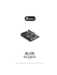
HSM/320 & /520
SYSTRONIX®
Dallas High Speed Microcontroller
Development System
801-534-1017
www.systronix.com
Prototype quickly
using the new
Dallas High Speed
Microcontroller
Family with the
HSM/320 & /520
from Systronix.
July1999 version
now supports
DS87C520 at 33
MHz. Includes
enhanced firmware
plus new RAD51
IDE& assembler!
The hot new
HSM/320 & /520.
8.3 MIPs. 128 KBytes
NVRAM. 2 UARTs.
Windows RAD51
assembler & IDE.
Only $99-$179.
ion
s
r
e
V
New
1999
y
l
u
J
ng
Shippi
What are you waiting for? Kick
your 8051 application into warp
drive. HSM/320 was designed
with a clean sheet approach to
maximize performance from the
radical new Dallas High Speed
Micros. It delivers true zero waitstate 33 MHz performance.
Easy program loading from a PC
serial port. No jumpers to change
or chips to unplug.
Use our BCI51PRO BASIC
compiler - or new RAD51
assembler and IDE.
Accept no substitutes. Take no
prisoners.
• 5-13VDC power input, on-board
voltage regulator
• All processor ports brought out to
clearly labelled headers
• Dual UARTs, dual RS232 ports
• 2 test pushbuttons (high & low) and 2
test LEDs need only 1 mA drive
• Generous prototyping area for SMT
SOIC (wide and narrow), and
through-hole DIP, SIP & ZIP
• 128 KBytes NVRAM, true zero waitstate 33 MHz performance.
• Powerful serial loader& utility EPROM.
• Assembler and example programs.
• Standard 100mm by 160mm size
• Technical data and secure on-line
ordering at www.systronix.com
What are Dallas High-Speed Microcontrollers?
Dallas High Speed Microcontrollers (HSMs) are high performance, low power,
CMOS 8051 code-compatibles with a radical new processor core. Instead of a
generic 8051's 12 clocks per instruction cycle, the HSMs complete an instruction
cycle in only 4 clock periods. Combine that 3X performance boost with clock
speeds up to 33 MHz and you've got an 8.3 MIP CMOS controller!
Other unique features include five external interrupts, an on-board watchdog timer,
power-fail interrupt, dual UARTs, dual data pointers, and flexible powerconservation options. For data, contact Dallas Semiconductor at 972-371-4000 or
www.dalsemi.com, or follow the links from www.systronix.com.
True 33 MHz Zero Wait-State Performance
The High Speed Micros have improved I/O Port capacitive load drive capability,
especially on Port 0. This is different enough from generic 12- and 16- MHz 8051s
to merit careful system design. Add the timing requirements of 25- and 33- MHz
memory access and it's clear that just stuffing an HSM controller into an old, slow
8051 board will only deliver part of the performance you could have. HSM/320 is
rigorously designed to meet all manufacturer's timing requirements over worst case
temperature and power variations, with no wait states. Accept no substitutes.
Full 128 KBytes of Code and Data NVRAM
The High Speed Micros have the same 16-bit address space as 8051s, for up to 64
KBytes each of code and data. HSM/320 delivers with a full complement of
memory. Systronix proprietary memory interface circuitry combines a 128Kx8
SRAM, a CMOS PLD, a MaxCap, and a power-control supervisor chip. The
result is 60 KBytes each of code and data (both are nonvolatile), and a 4 KByte
memory mapped I/O space.
Smart Loader/Demonstrator EPROM
The powerful Systronix auto-bauding loader does much more than program HEX
files into the development board's NVRAM. You can read and write all controller
registers, internal data and external data memory, set stretch cycles,test interrupts,
and more. You can peek and poke all memory-mapped I/O space - very handy for
testing peripherals you've added. All of this can be done manually or via script files
sent from an RS232 serial port of ANY computer - Wintel, Mac, Linux, SUN,
whatever. All you need is a basic communications program.
Includes new Systronix RAD51 IDE and 8051 Assembler
HSM/320 & /520 include the new Systronix RAD51 Integrated Development
Environment (IDE) and 8051-family assembler. Requires Windows 95/98/NT. 16bit Windows and DOS tools are also included.
DETAILED DESCRIPTION
Processor socket & support DIP40 for any 5-volt
DS80C320 family member including DS87C520. Code can
be located in the internal EPROM of applicable family
members by changing a board jumper. Internal 1 KBye of
data memory of DS87C520 can be used seamlessly in
conjunction with 60 KBytes of on-board data memory.
Memory 128 KByte NVRAM (120 KBytes usable)
divided into 60 KBytes of code and 60 KBytes of data.
NVRAM is backed up with a MaxCap for 3-4 week
typical power-off nonvolatility.
Power Unregulated 6-13 VDC or 5 VDC regulated. 5.5x2.5
mm unregulated input power jack. Regulator is reversepolarity, short-circuit and over-temperature protected.
Serial I/O Two RS232 serial I/O (DB9M), one for each
UART in the 80C320/520. The RS232 buffers can be
disconnected if you wish to add your own buffer for
RS485, RS422, etc.
Prototype Area Generous 5.3 x 1.4 inch prototype area.
Dual strips of SOIC-to-through hole pads on front and rear
of board. Perfect for prototyping with surface mount
devices. Heavy power and ground busses on .025" headers.
Every pad is surrounded by ground plane - perfect for lownoise analog circuitry. Front of proto area plane is VCC,
back is GND, with exposed diamonds in the solder mask
for easy power and ground connection.
Expansion Memory mapped I/O space at FXXXH is
decoded and brought out to a .025" post. A 16V8 DIP20
PLD fits perfectly below the A0-A15 bus headers to
simplify additional decoding or strobe generation.
Easy Program Loading Serial program loading can be
initiated by on-card pushbutton. No special software is
needed - use any terminal communication program on any
brand of computer. LEDs indicate RUN and LOAD
modes. The serial loader is only active in LOAD mode. In
RUN mode it is inactive, giving your program complete
control of all controller memory and resources.
Size Standard 100x160 mm single Eurocard size, hundreds
of enclosures available (some stocked by Systronix)
including RF shielded, NEMA rated, etc.
Related Products
Environmental Commercial temperature 0 to 70 deg C.
Systronix now also supports the Dallas DS87C530 with an adapter which plugs
onto the basic HSM/320 board. HSM/550 supports the new Dallas DS87C550
EPROM/ADC/PWM High Speed Processor.
Support & Warranty Unlimited friendly technical
support. One year warranty against defects.
HSM/320: $see website or call
33 MHz HSM/320 with 33.0000 and 22.1184 MHz crystals. Complete
system with manual, power cube, and software.
HSM/520: $see website or call
All systems include:
33 MHz HSM/520 board with DS87C520 controller, either plastic OTP or
ceramic window erasable. Includes same crystals and accessories as HSM/320.
· Printed user manual (on disk in Lite version)
Lite: $see website or call
· Schematics (on disk in Lite version)
22 MHz system, without controller or power cube, and with manual on disk.
· Sample programs in RAD51 assembly code and Systronix
BCI51 Real-time Compiled BASIC
rev 2009 Jun 11 bab
Systronix Inc.
®
939 Edison Street Salt Lake City, Utah, USA 84111
Tel:(801)-534-1017 www.systronix.com
HSM/320 & HSM/520 Technical Reference 2.0 - October 6, 1999 - © Systronix®
HSM/320 & HSM/520- READ THIS FIRST
Thank you for purchasing the High Speed Microcontroller/DS80C320 (HSM/320) or the
HSM/520 Development System! If you really hate reading manuals, then go ahead and hook up
the board - COM1 is used for program loading. The loader will auto-baud to a carriage return
sent from your PC. Follow the rest of the instructions on the back of the board. If you get stuck,
come back here.
It's tempting to jump into a complex application right off the bat, but please run one of the
supplied sample programs first. This will verify that your PC, cable, hardware and installed
software are all working together, and that you understand the complete assemble- or compileand-download process.
Most of the problems people have getting started are serial cable or PC serial communications
related. So be sure your PC serial port is properly connected and configured. We test every
HSM/320, and its serial port is quite rugged, so it is highly unlikely that the HSM/320 serial port
is the problem. Refer to the troubleshooting section for more tips.
Remember: use a straight through serial cable (not a null modem cable), and connect to the
board’s COM1, not COM0. Then send the loader a carriage return (^M, 13 decimal, 0D
Hex, or 0x0D, usually the ‘enter’ key). More than half of the support calls we receive are
related to these simple issues, usually because a new user didn’t even read the “quick start”
section of this manual. Obviously, you’re not making that mistake - give yourself two points.
HSM/520 as an EPROM-based OEM Controller
Perhaps the HSM/320 is ideal for your development, but you want to install your finished
system and never have to worry about losing the program, even after several weeks without
power. There is a way to do this - if 16 Kbytes of code is enough for you. The DS87C520
controller has 16 Kbytes of EPROM and 1 Kbyte of SRAM, so it makes a very capable
single-chip controller. Systronix stocks both OTP and erasable versions of the DS87C520.
Here’s how to do it. Develop with a DS80C320 installed, or with a DS87C520, as long as
JP5 is in the ‘EXT’ position (so that the loader is active). When development is done, burn
your code into a DS87C520 and set jumper JP5 to the ‘INT’ position. Now after any reset or
power-up condition, the DS87C520 will execute code out of its internal EPROM. Your
application will still have access to all the external data space of the board, plus code above
1
HSM/320 & HSM/520 Technical Reference 2.0 - October 6, 1999 - © Systronix®
16 Kbytes (4000H and above). To go back to development, just move JP5 to the ‘EXT’
position and the DS87C520 internal EPROM is ignored.
Versions
HSM/320 was developed in conjunction with Dallas Semiconductor to be a simple, low cost
80C320 family development board. The current revision of the circuit board is “C”.
HSM/320 is specifically designed to support the entire Dallas High-Speed Microcontroller
family in the DIP40 package.
Formerly called “HSM/KISS”, we changed the name in summer of 1999 when we added two
important new capabilities. First, the new loader/demonstrator is now auto-bauding
regardless of controller crystal, and has many new features. We changed to faster PLDs,
SRAM, and EPROM to support the timing of the DS87C520 controller (yes - the DS87C520
has different memory timing than the DS80C320).
The silkscreen on HSM/320 boards still identifies them as “HSM/KISS”. This will be
changed the next time we run bare boards. You can be sure you have the newer board if the
label on the loader is “HSM UNI”. These boards have 10 nsec PLDs, 55 nsec SRAM, and 45
nsec EPROM to support the 87C520 timing.
HSM/320 is available in two versions: 33 MHz, fully populated, and a 22 Mhz Lite version.
HSM/520 is available only in a 33 MHz, fully populated version. You can convert a later
version of HSM/320 to HSM/520 by plugging in a DS87C520 controller.
The HSM UNI rev D or later loader/demonstrator is 87C520-aware, earlier versions are not.
For simplicity, we refer to the current version of the board with the rev D or later
loader/demonstrator as the HSM/320, recognizing that simply adding a DS87C520 controller
makes it an HSM/520.
Errata
The silkscreen on HSM/320 boards still identifies them as “HSM/KISS”. This will be
changed the next time we run bare boards.
On revision B and some revision C boards, the silkscreen legend for test points T1 and T4 is
incorrect. T1 is FXXX(L) and T4 is RUN(L). The function of the pins is correct, just the
silkscreen got swapped. This was corrected in a later run of Rev C boards.
We are in the slow process of adding special support for the Dallas High Speed Micros to the
BCI51 Pro real-time BASIC compiler. At the moment, you must treat the HSM family like
80C32s running faster. Please see the section “Using BCI51 Pro with HSM/320” for more
information. Check into our Web site for the latest news on the HSM support in BCI51 PRO.
2
HSM/320 & HSM/520 Technical Reference 2.0 - October 6, 1999 - © Systronix®
This is not exactly errata, it’s more of an unavoidable quirk, but here it is. The loader W
command writes to memory or I/O space using the movx instruction. It also attempts to verify
what was written by reading at the same address. This will find memory problems or some
memory mapped I/O register problems. However, some memory mapped devices are writeonly, or for other reasons don’t allow you to read the same data you wrote. In that case you’ll
see a loader warning about a verify failure. That’s the quirk - the verify failure may not be
real for your specific I/O device.
Terminology in This Manual
We use a fixed pitch font to represent what you see or type on your PC:
C:\HSMK\ASM BLINK
F
We use the pointing hand to call attention to something worthy of special note, such as a
common pitfall or interesting feature of HSM/320.
What You Need to Use HSM/320
4
To power up the HSM/320 board, you need a 6-12 VDC unregulated source such as the
Systronix #5003 6VDC 800mA power cube shipped with all but the lite version of HSM/320.
If you use your own cube, be sure the center terminal of the 5.5 x 2.5 mm jack is positive 6 to
12 volts DC. The sleeve is negative. An AC power cube could damage HSM/320.
4
To connect HSM/320 to your PC serial port, you need a straight-through cable from your PC
to a DB9 female, to mate with the DB9 male on HSM/320. Systronix #9210 serial adapter kit
contains a 6 foot/ 2 meter DB9 extension cable, a DB9 to DB25 adapter, and DB25 and DB9
gender changers.
4
To download a program to HSM/320, and communicate with the HSM/320 serial loader, you
need any serial communications program such as Windows Terminal or Windows 95
Hyperterminal. You can use any computer, not just a PC-compatible, as long as it supports
RS232 communication.
4
To assemble a program for use on HSM/320, you need an 8051 assembler such as the
Systronix Windows RAD51 assembler, or the older DOS A51 assembler, both included with
HSM/320. Or you can use any 8051 family development tool, running on any computer
platform of your choice, as long as it generates a standard Intel HEX file. Binary file loading
is not supported by HSM/320.
4
To understand the High Speed Microcontroller family, you need the Dallas High Speed
Microcontroller data sheets and application notes, available from www.dalsemi.com, or by
calling Dallas Semiconductor at 972-371-4000. We’ve include the 80C320 data sheet in PDF
format on your HSM/320 disk.
3
HSM/320 & HSM/520 Technical Reference 2.0 - October 6, 1999 - © Systronix®
4
The HSM/520 version of the board of course
requires a DS87C520 controller. The setting of the
ROM jumper JP5 (adjacent to pin 40 of the
controller) selects INT or EXT. In the INT position,
code memory in the DS87C520 internal EPROM is
enabled. In RUN mode, whatever program is in the
DS87C520 EPROM will boot up following a reset.
Quick Start - Step by Step
1) HSM/320 example files are part of the Systronix
CDROM. If your CDROM is more than a few
weeks old, the quickest way to get new files is to
load a new copy from the HSM files area of our
web site at www.systronix.com, or FTP it from
ftp.systronix.com. The CDROM will autorun under Windows 95/98. Follow the InstallShield
prompts to install the examples on your computer.
2) Connect the power cube to the HSM/320 J3 power jack. After application of power, the green
RUN LED will be lit. Press the LOAD switch and hold it for more about half a second. The
red LOAD LED should be on. If neither LED is lit, the board is not receiving power. Check
for proper power polarity - the center of the J3 power jack is positive.
3) Connect a DB9 female straight (not null modem) cable from your PC serial port to HSM/320
COM1 (near the prototype area). HSM/320 expects TXD on pin 2 and RXD on pin 3 of the
serial port cable. This sets up the PC as “DTE” (Data Teminal Equipment) and HSM/320 as
“DCE” (Data Communications Equipment) in RS232 parlance. A kit of adapters and a DB9
extension cable is available from Systronix at 801-534-1017 or www.systronix.com.
HSM/320 COM1 is the added UART of the Dallas 80C320, and is used by the serial loader
for program loading. HSM/320 COM0 is the normal UART available in most every 8051,
and is not used at all by the serial loader. HSM/320 must use COM1 for loading but you can
use any available PC COM port.
4) Start a terminal program such as Hyperterminal, set the communication parameters to your
desired baud rate (start with 9600 or 19.2 kbaud). Set other communication parameters to
“direct” connection (not through a modem), 8 data bits, no parity, 1 stop bit, Xon/Xoff flow
control. A Hyperterminal dialog box is shown to the right. Be sure to set the terminal
software COM port to the correct port on your PC. Save these settings. Now open a
connection in the terminal software, usually with a “connect” command or button.
5) Wait a second, to give the terminal program time to establish the connection to HSM/320.
Now press and hold the LOAD button for more than half a second. The LOAD button is next
to the red LED. When you release the button, the red LED should remain lit. If, instead, the
green LED lights, you need to hold the LOAD button longer before releasing it.
4
HSM/320 & HSM/520 Technical Reference 2.0 - October 6, 1999 - © Systronix®
F
Note that your board may have a factory test program left in it, so don’t be alarmed if it emits
serial output in RUN mode, even before you load any program of your own. We’ve seen
boards hold a program for more than a month, proof that the MaxCap backup circuitry
typically performs much better than its worst-case design minimums.
If your PC serial port is connected through a straight cable (TXD and RXD are not swapped),
and you press the LOAD button, and then press the ENTER key on your PC, you should
see the loader sign-on message. The loader must receive a carriage return in order to
synchronize itself to your PC’s baud rate. The message will look something like this. (The
exact appearance may vary with your specific loader version).
Unified HSM HEX LOADER Rev D.04 (08/31/99)
(C)1996-1999 SYSTRONIX, INC.
Type "?" for command help
6) If you enter a question mark for help, you should see something like this (again, the exact
appearance will depend on your loader version):
520> ?
---------- Loader Commands ----------------------------------------L
;load intel HEX file
D [start [end]]
;dump HEX file
V
;verify HEX file w/memory
T
;toggle HEX file echo
I
;toggle all external interrupt enables
C [start [end]]
;calc CRC-16
E
;erase xdata to 0FFH
F value [start [end]]
;fill xdata with value
G
;get port values
P val0 val1 val2 val3
;put valx to portx...
;...except TXD1, RXD1, RD, WR of P1 & P3
WX adr val
;write val to adr in xdata or I/O space
WI adr val
;write val to adr in internal data space
WR adr val
;write val to adr in SFR space
RX adr
;read at adr in xdata or I/O space
RI adr
;read at adr in internal data space
RR adr
;read at adr in SFR space
M
;Memory test with exhaustive patterns
A
;Address line test
X value
;show/change movx stretch value (0-7)
-------------------------------------------------------------------Press any key to continue . . .
WD val
;write val to system DAC (550 only)
Memory: code=0000-EFFFH, xdata=0000-EFFFH, I/O=F000-FFFFH
All values are entered and displayed in hexadecimal format
memory errors display as {address}:{should be}/{actual}
Loader has detected DS87C520 processor
520>
7) Try sending one of the sample HEX files to HSM/320. To send a HEX file to HSM/320, type
an “L” for LOAD followed by a carriage return (Enter key), and then send the HEX file from
your terminal software. If the loader receives the file with correct checksums, you will get an
“OK” response. If there are load errors, the loader will tell you as they occur.
5
HSM/320 & HSM/520 Technical Reference 2.0 - October 6, 1999 - © Systronix®
It's tempting to jump into a complex application right off the bat, but please run one of the
supplied sample programs first. This will verify that your PC, cable, hardware and installed
software are all working together
If you are using assembly code, we’ve included example files “HELLOXX.ASM” and
HELLOXX.HEX where XX is a code for the crystal of your HSM/320. The XX is 22 for
22.1184 Mhz, and 33 for 33 Mhz. For a quick test of your system, load the appropriate
HELLO hex file.
If you are using BCI51 Pro compiled BASIC, compile the file HELLO.BAS, making sure that
the #XTAL declaration matches the crystal of your board. There are comments about this in
the file HELLO.BAS.
8) To run your loaded file, move the HSM serial cable to COM0 (the default HSM/320 “user”
serial port). You may need to use different communication settings if your test program and
loader baud rate are different. Now press and release the HSM/320 RESET button. The
green RUN LED should light, and your sample program will emit a repeating message to
your terminal software screen. Since the serial loader always uses HSM/320 COM1 and
generic 8051 code will always use HSM/320 COM0 for serial I/O, you can leave both serial
ports connected - COM1 to your PC, to load the program to be tested, and COM0 to another
PC, modem, or other serial device which you are controlling.
If your PC is capable, you can keep two communication software windows open - one to the
loader COM1 and another to your application’s COM0. They can be different baud rates if
you wish.
9) That’s it! You should be up and running. If you had problems, check your PC serial port
connection and refer to the troubleshooting portion of this technical reference.
HSM/520 Differences and Considerations
The DS87C520 is very similar to the DS80C320. The C520 has 16 KBytes of internal code
EPROM, and 1 KByte of so-called ‘movx’ or ‘xdata’ SRAM. There are additional memory
control registers in the C520. Memory timing is also different from the C320. Otherwise, the
controllers are identical.
DS87C520 controllers are available in erasable or one-time-programmable (OTP) versions.
They must be programmed in a device programmer. You cannot program the DS87C520 in
the HSM/520 board.
DS87C520 Code Memory Selection
The HSM/520 version of the board implies that you do have a DS87C520 controller installed.
The setting of the ROM jumper JP5 (adjacent to pin 40 of the controller) selects INT or EXT.
6
HSM/320 & HSM/520 Technical Reference 2.0 - October 6, 1999 - © Systronix®
In the EXT position, the 87C520's internal CODE memory is disabled, so it functions much
like a no-EPROM C320. In LOAD mode the DS87C520 executes code from the HSM/320
loader EPROM. In RUN mode it will attempt to execute code from the NVRAM code page.
In the INT position, code memory in the DS87C520 internal EPROM is enabled. In RUN
mode, whatever program is in the DS87C520 EPROM will boot up following a reset. In
LOAD mode, the same is true. In both modes, then, the HSM/320 loader is not accessed.
DS87C520 Data Memory Selection
The DS87C520 has 1 Kbyte of on-board ‘movx’ or ‘xdata’ SRAM. This SRAM must be
explicitly enabled to be accessed. The C520 data sheet describes this. If enabled, then that
portion of the HSM/320 board’s data SRAM will not be accessed. All xdata accesses which
lie outside of the address range of the active internal xdata SRAM automatically go to boardmounted HSM/320 SRAM.
Confused? The 1 Kbyte of SRAM which is physically internal to the DS87C520 is
nevertheless accessed with ‘movx’ instructions, so it is treated by the controller as ‘external’
data memory. Application code can’t tell any difference between the DS87C520 SRAM and
physically external SRAM.
The total xdata address range is still 64 Kbytes, you don’t get the 64 Kbytes of external
SRAM plus the internal 1 KByte. However, you could turn on the internal SRAM, write to it,
disable it, and use the external SRAM. When you need to access the internal xdata memory,
just enable it again.
With the internal xdata memory and the 16 Kbytes of EPROM, the 87C520 is capable of
storing and executing fairly large applications in “single chip” mode, with no external
memory.
BCI51 and DS87C520 as a Single Chip Design
If you are using BCI51 Pro to compile a BASIC program for the DS87C520 in single chip
mode, you will need to modify the BCI51 startup code to enable the internal xdata SRAM. 1
Kbyte is enough for the BCI51 serial I/O buffers plus several hundred BASIC variables. If
you don’t find this information on our web site, email us ([email protected]) for the
details.
7
HSM/320 & HSM/520 Technical Reference 2.0 - October 6, 1999 - © Systronix®
8
HSM/320 & HSM/520 Technical Reference 2.0 - October 6, 1999 - © Systronix®
HSM/320 DETAILED DESCRIPTION
Philosophy and Purpose of HSM/320
There are a lot of 8051 development boards on the market, so why did we develop
HSM/320? First of all, it is designed from the ground up to be optimal for the Dallas High
Speed Microcontroller (HSM) family. There are some differences between generic 8051s and
the HSMs. Just plopping an HSM into an 8051 socket will probably not give you the best
performance, and will probably not even work at 22 Mhz or above. These differences are
detailed in a separate section of this manual.
a. Easy to use demo/development board for the Dallas High Speed Micros.
b. LOW COST - even though complete with 60 KBytes each of code and data memory
(we sell no boards with empty sockets as some vendors do to advertise a low price).
c. Simple development and experimentation board. No dedicated I/O devices, so all I/O
pins are available for your use. HSM/320 does decode the upper 4 Kbytes of xdata
for your use as I/O space.
d. Designed for prototyping and development - generous through-hole and surface
mount prototype areas, clearly labeled access to all controller pins.
e. Easy to use - all you need to load a program is a PC with a serial port.
f. Built in serial loader for easy program loading and testing. Loader is non-intrusive in
RUN mode, meaning it uses no memory or processor resources.
g. High Speed - designed for use at up to 33 MHz with no data “stretch” cycles. In order
to run at full speed, HSM have special needs compared to generic 16 MHz 8051s.
HSM/320 has been designed specifically for the HSM family. “Accept no
substitutes”.
HSM/320 Versions
HSM/320 is available in 25 and 33 MHz versions as shown in this table. These prices are in
$US and are subject to change at any time. Check our web site, online store, or call for
current pricing. To create an erasable HSM/520 system please order a DS87C520 controller
in addition to the HSM/320 Pro or HSM/520 development systems.
9
HSM/320 & HSM/520 Technical Reference 2.0 - October 6, 1999 - © Systronix®
HSM/320 & /520 VERSIONS
Version:
Crystal
MCU
HSM/320
25 MHz
Lite
HSM/320
33 MHz
Pro
22.1184
none
33.0000
33.0000
HSM/520
(33 MHz
only)
Loader
PROM
70 nsec
128Kx8
NVRAM
70 or 55 nsec
control
PLD
15 nsec
Power
Cube?
none
Docs
Price
on disk
$99
80C320
33 MHz
45 nsec
55 nsec
10 nsec
6V 800 mA
printed
$149
87C520
OTP
33 MHz
45 nsec
55 nsec
10 nsec
6V 800 mA
printed
$165
HSM/320 Features
DIP40 socket for 80C320-family High Speed Microcontrollers.
a. 128Kx8 NVRAM with MaxCap backup, divided into a 64 Kbyte code page and a 64
Kbyte data page. Backup retains code and data for two months (typical at room
temperature) without system power. On board circuitry protects the NVRAM from
invalid write cycles during power up and power failure conditions. 4 Kbytes of each
are unusable since that is mapped as I/O space.
b. On-board serial loader accepts a HEX file from UART1. Leaves UART0 untouched.
Use any terminal program to transfer the file. Does not use DTR to trigger load mode.
c. Serial I/O: RS232 on UART0 and UART1. RS232 I/O can be cut from the processor
to enable wiring to a custom I/O chip in the prototype area.
d. Early power fail interrupt provides time for orderly system shutdown.
e. On-board regulator with heatsink, 6-12 VDC input, 5.5x2.5 mm power jack.
f. Push-button high drives one or more of Int2 or Int4 (jumpers select).
g. Push-button low drives one or more of INT0,1,3,5 (jumpers select).
h. LEDs to indicate load (red) or run (green) status.
i. Two LED test points - LED lights when point is driven low. Requires less than 1 mA
of low sink capability on the driving source, so can be driven by any port pin.
j. Microcontroller supervisor and reset circuitry, with early Power Fail Warning
interrupt to INT0 (can be isolated if you don’t want PFW driving INTO).
k. Generous prototyping area for DIPs and also an SMT proto area! Proto area has a
power plane on the front side of the board and a ground plane on the back. Multiple
solder pads for power on the front and ground on the back make connecting your own
chips quick and easy.
l. All processor signals brought out to headers, labeled on both sides of the board for
easy wiring and probing.
m. Serial loader accepts Intel Hex files from any terminal communication program. The
serial loader is active only in LOAD mode. In RUN mode it is mapped out of
processor memory and does not use any processor resources. Our serial loader is
completely non-intrusive.
10
HSM/320 & HSM/520 Technical Reference 2.0 - October 6, 1999 - © Systronix®
n. Standard Euroboard 160x100 mm size, conforms to ANSI/IEEE Std 1101/1987, IEC
297-3-1984, and other international standards. HSM/320 fits Systronix enclosures and
many others.
Loader and PLD Options and Updates
The HSM/320 serial loader and control PLD have no known bugs. If you do discover a bug
and we can duplicate it, we’ll ship you a new loader PROM or PLD at no charge.
We are planning to add additional features in future releases, and we welcome your input.
Revised versions of the serial loader and PLD will be available at a nominal charge (please
refer to the High Speed Micro Price List, available soon at www.systronix.com, for current
pricing). Please contact us if you would like a special version of either device.
The serial loader and memory control PLD, and their associated circuitry are copyrighted by
Systronix, Inc, with all rights reserved. Purchasing HSM/320 does not give you the right to
duplicate either device. If you wish to use the loader or PLD in your own products, we can
provide programmed parts or a license to create your own, at a very reasonable price.
Systronix Web Site & Forum
Our web site (www.systronix.com) is the main repository for new HSM/320 example code
and documentation. You can also join a forum of Systronix users. Our web site has
information about the forum.
Getting Technical Support
Our technical support is included with your purchase of HSM/320. We believe good support
begins with good written documentation (starting with what you’re reading right now). If you
can’t find the answer in our documentation, then try the FAQ on the web at
www.systronix.com, send e-mail to [email protected], call us at 801-534-1017, or Fax
us at 801-534-1019. When you contact us, please tell us about any errors or weaknesses in the
documentation so that we can improve it in the next revision.
If you can, please contact us by e-mail first. You can attach a file of source code and captured
output (use MIME encoding if possible) to your message. If you send us an example of a
problem please make the example as simple as possible, and include any necessary I/O driver
“include” files if you have modified them. We try to answer all e-mail within one or two
business days. Our web site is the main repository for new example code, application notes,
and I/O drivers.
Please feel free to contact us with any unusual questions about programming HSM/320. We
can probably help you approach your needs in the most efficient way. That's why we're here!
11
HSM/320 & HSM/520 Technical Reference 2.0 - October 6, 1999 - © Systronix®
Customers consistently give us high marks for our technical support. Tell us how well we're
doing for you.
Installing and Using the BCI51-Pro Basic Compiler
BCI51 Pro and the HSM Family
If you purchased BCI51-PRO, install it now, according to the instructions provided with it.
Please note that the A51 assembler is always provided with BCI51 Pro. The BCI51 compiler
invokes the assembler automatically, and you can also use A51 independently of the
compiler.
At this time there is no explicit support for the High Speed Micros in BCI51 Pro. Use an
8032 or 80C32 as the target. We will be adding support for the HSM special capabilities as
soon as we can. Please email us if you would like to be on the HSM/BCI51 tester list. You
must have email with MIME-encoded file attachment support to be on this list (Eudora and
most other popular email programs support MIME encoding).
At the moment, the following special features of the HSM family are not supported by
BCI51:
Baud rate is 19.2 kbaud max
The extra serial UART is not supported by BCI51 (the HSM/320 serial loader does use it)
The on-chip 1KByte of xdata RAM of the DS80C520 is not supported
Data stretch uses the default value.
The console auto baud option does not work properly in the HSM family, because the
instruction timing is different.
HSM/320 Example Program Files
HSM/320 example files are in the self-extracting archive HSMK_XMP.EXE. Some of the
example files will overwrite BCI51-Pro files. This is OK.
File Extensions .SRL and .INC
The file extension .SRL stands for “Source Library”. SRL files contain serial I/O drivers,
math operations, and other library support code to implement the BASIC-language syntax in
BCI51 programs. Include files with an extension “.INC” are used to implement functions
which are not part of BCI51 BASIC such as LCD access, analog-to-digital conversion,
keypad input, and so forth. Sample I/O drivers are included. You can modify them to support
similar I/O devices which you add to HSM/320.
First Program
Try the example program “hello.bas” provided in the file HSMK_XMP.EXE as your first use
of HSM/320 and BCI51.Open the .BAS program file with any text editor and make sure your
12
HSM/320 & HSM/520 Technical Reference 2.0 - October 6, 1999 - © Systronix®
target is an 80C32 and code start and data start are both 0. XTAL should be 22118400 for 25
MHz boards (the crystal package is printed with “22.1", or 33000000 for 33 MHz boards.
Save the file as plain ASCII text. Your HELLO.BAS should look something like this:
;Simple Hello program for HSM/320
#target 80C32
#xtal 22118400
#code start 0
#data start 0
#console mode=19200
#check math off
; 22.1184 MHz
; 19.2 kbaud
unsigned integer X
main:
ph1. "HSM/320 COM0 at 19.2 kbaud, X=", X
x = x+1
goto main
END
Compile your program by invoking BCI51 on it. For example, at the DOS command line, or
in DOS window, type (commands are not case sensitive)
bci51 hello -o
The switch “-o” (the letter o, not the numeral 0) invokes the BCI51 optimization option.
After the compilation is complete, this will create a file HELLO.HEX.
Connect a standard (all pins wired straight through) serial cable from your PC to HSM/320
COM1. Do not use a null modem cable (pin 2-TXD and pin3-RXD swapped). Start a
communications program such as Windows Terminal, Procomm, or similar, on your PC. Set
the baud rate to 19,200 with a data format of 8/N/1, simple ASCII terminal emulation.
Connect the power cube to HSM/320. Press the LOAD switch for about one second and the
red LOAD LED should turn on, and you will see a sign-on message on the PC similar to this
(yours may vary with new loader versions):
320>
Unified HSM HEX LOADER & DEMONSTRATOR Rev xE.00
(C)1996-1999 SYSTRONIX, INC.
Type "?" for command help
320>
If you enter a question mark for help, you should something like this (the exact appearance
will depend on your loader version). Loader commands are described in detail in another
section of this manual.
13
HSM/320 & HSM/520 Technical Reference 2.0 - October 6, 1999 - © Systronix®
?
---------- Loader Commands ----------------------------------------L
;load intel HEX file
D{I|R}
;display content of idata or SFRs
DX [start [end]]
;display content of xdata
V
;verify HEX file w/memory
T
;toggle HEX file echo
I
;toggle all external interrupt enables
C [start [end]]
;calc CRC-16
E
;erase xdata to 0FFH
F value [start [end]]
;fill xdata with value
W{I|R} adr val
;write val to adr in idata or SFR space
WP port val
;write val to port
WX adr val
;write val to adr in xdata or I/O space
R{I|R} adr
;read at adr in idata or SFR space
RP port
;read port
RX adr
;read at adr in xdata or I/O space
M
;Memory test with exhaustive patterns
A
;Address line test
X value
;show/change movx stretch value (0-7)
-------------------------------------------------------------------Press any key to continue . . .
To send the file HELLO.HEX to HSM/320, enter L at the loader prompt. The loader then
waits for a HEX file. In Terminal, use the “send text file” menu option and specify
HELLO.HEX as the file.
To run HELLO, switch the serial port cable to HSM/320 COM0, and press the reset&run
button. The green RUN LED should turn on and your program should display something like
this:
HSM/320
HSM/320
HSM/320
HSM/320
HSM/320
COM0
COM0
COM0
COM0
COM0
at
at
at
at
at
19.2
19.2
19.2
19.2
19.2
kbaud,
kbaud,
kbaud,
kbaud,
kbaud,
X=0000H
X=0001H
X=0002H
X=0003H
X=0004H
and so forth.
If this all worked correctly, you’re on your way and ready to write your own program. If not,
please refer to the troubleshooting section before contacting us.
Installing and Using the Windows RAD51 IDE & Assembler
RAD51 requires 32-bit Windows such as Windows 95, 98 or NT 4.0 or later. It is not
compatible with Windows 3.X and also may not work correctly with NT 3.X. RAD51 installs
with its own “setup.exe” install program. Online documentation for the assembler is
included. The assembler syntax is the same as the DOS A51 assembler.
14
HSM/320 & HSM/520 Technical Reference 2.0 - October 6, 1999 - © Systronix®
Installing and Using the DOS A51 Assembler
We recommend you use the new RAD51 Windows IDE and Assembler. However, if you will
be using the A51 DOS assembler, install it now. Just copy the file A51.EXE from the diskette
into the desired directory on your hard disk.
Invoke A51 With a Batch File
Instead of typing a long command line to invoke A51, use our batch file ASM.BAT. Just
invoke the batch file followed by the .ASM file which you wish to assemble:
C:\HSM\A51 HELLO
Here’s the contents of ASM.BAT. “%1" is the filename you pass to the batch file on the
command line.
Echo off
Echo assembling %1.asm with A51
a51 %1.asm -o %1.hex -l %1.prn
Detailed documentation for the DOS assembler A51 is available in a PDF file on your
installation disk.
HSM/320 Memory
HSM/320 Memory Map in Load and Run Mode
HSM/320 uses a single 128Kx8 SRAM with nonvolatile control logic and a capacitor backup
to make this a 128Kx8 NVRAM (nonvolatile RAM) device. The PLD in location U7 splits
the NVRAM into two pages. Page0 is the lower 64 Kbytes and Page1 is the upper 64 Kbytes.
The 4 Kbyte memory-mapped I/O space disables the upper 4 Kbytes of each page.
While executing out of the serial loader, the code page of the NVRAM is mapped into the
data space of the controller. This enables the loader to write to what will be the code page (in
RUN mode) of the NVRAM. It also prevents the controller from accessing any external data
memory while in LOAD mode. Therefore the loader firmware is written to use only internal
data memory. The table HSM/320 Serial Loader Modes and NVRAM Memory Access
describes the relationship between load and run modes and NVRAM page access.
15
HSM/320 & HSM/520 Technical Reference 2.0 - October 6, 1999 - © Systronix®
HSM/320 Serial Loader Modes and NVRAM Memory Access
Reset Type:
Power-On
Reset
Reset/Run
Pushbutton
Load
Pushbutton
Code Space
NVRAM page0
(user program)
NVRAM page0
(user program)
Data Space
NVRAM page1
(user data)
NVRAM
(user data)
LED
green
Controller Hardware
hard reset hard reset
green
hard reset
hard reset
Serial loader in
ROM
NVRAM page0
(temporarily
mapped into
data space for
program load &
verify)
red
hard reset
hard reset
Reset/Run Mode: Power on reset resets the controller and causes execution to begin in the
code page of the NVRAM. The RESET push-button also resets the controller and causes
execution to begin in the code page of the NVRAM.
Load/Program Mode: Pressing and holding the LOAD push-button resets the controller as
the reset button does. But if you continue to hold the load button down for a half second or
so, execution starts in the serial loader.
Serial Loader 100% Non-intrusive in RUN Mode
The serial loader is active only in LOAD mode. Our proprietary memory control PLD
provides this function. In RUN mode, the serial loader is mapped out of processor memory
and does not use any processor resources. In RUN mode the serial loader EPROM is placed
in a low-power, inactive state. In RUN mode our serial loader is completely non-intrusive and
will not interfere with your application program in any way. This is a very important
capability, and one of the nicest features of HSM/320.
The serial loader includes other functions such as memory test, reading and writing to
controller ports, SFRs, and so forth. It is not a monitor, so it cannot be accessed from your
application program, and cannot set breakpoints, single-step your program, and other typical
monitor functions.
16
HSM/320 & HSM/520 Technical Reference 2.0 - October 6, 1999 - © Systronix®
THE SERIAL LOADER & DEMONSTRATOR
Description
What is the “Smart Autobauding Loader/Demonstrator”?
That’s a rather ungainly name, but it was the best we could think of. (We’re not an ad agency,
just a bunch of acronym- and technology- loving engineers). The loader provides Intel HEX
file transfer, memory fill, HSM Port read and write, SFR access, I/O space peek and poke,
and much more. I/O space “peek and poke” is really just I/O space “read and write” but
“peek and poke” sounds like more fun, doesn’t it? You can use any terminal emulator or
communications program which supports standard RS232 serial I/O. You don’t need a
“Wintel” PC.
Tips & Tricks
Automate Your Testing with ‘Script’ Files
In load mode, you can of course send a series of keyboard commands to the loader. This
could include erasing memory, writing and reading memory-mapped I/O space, sending a
HEX file and so forth. “OK”, you say, “maybe that’s cool but where’s the tricky part?”
Here it is: you can prepare an ASCII text file with these commands, one per line. Then send
the file to HSM. In Hyperterminal it’s Transfer->Send Text File. You will need to set the
File->Properties->Settings->ASCII Setup->Line Delay to 500 or 1000 msec, to give the
loader time to process the command. If your communications software supports macros or
scripts, so much the better. We’ve included some sample files we use with Hyperterminal.
More are on the web site.
This is a simple and powerful way to test register settings before you take the time to create a
program. It’s much easier to debug a configuration problem at the loader command line, than
within a program. We use this approach a lot in our own test and debug work here. That’s
17
HSM/320 & HSM/520 Technical Reference 2.0 - October 6, 1999 - © Systronix®
why we took the trouble to add these features to the loader - we thought you’d find them
useful too.
Supported Baud Rates
The Loader/Demonstrator syncs to many standard baud rates from 600 to 57,600 baud
depending on the controller crystal. Note that with a 33 MHz crystal, 38,400 baud error is
greater than 3% and may not be reliable. Crystals on the HSM board and in your PC are not
perfect, especially at temperature extremes, so you may find that your PC does better or
worse than the table indicates. For example, one new NT workstation here at Systronix
World HeadQuarters (WHQ) does fine with a 33 MHz HSM at 38400 baud, while another
identical workstation occasionally receives garbled characters.
HSM Loader/Demonstrator Baud Rates
Crystal
33.000
MHz
22.1184
MHz
14.7456
MHz
11.0592
MHz
10.000
MHz
20.000
MHz
40.000
MHz
60
0
Y
120
0
Y
240
0
480
0
960
0
1920
0
3840
0
57600
Y
Y
Y
Y
error
>3%
Y
300
Y
Y
Y
Y
Y
Y
N
150
Y
Y
Y
Y
Y
?
N
150
Y
Y
Y
Y
Y
N
N
Y
Y
Y
Y
Y
Y
Y
N
Y
Y
Y
Y
Y
Y
Y
N
Y
Y
Y
Y
Y
Y
Y
Y
Starting and Connecting to the Loader/Demostrator
The HSM serial loader/demonstrator uses the HSM second serial port (COM1 on the HSM
board). If your board uses an external EPROM for the loader, it typically resides in a 27C256
EPROM or equivalent. Your board’s ROM select jumper must be in the “EXT” position to
drive the HSM’s EA (External Access) pin low. Normally, we ship all boards with this
jumper in the EXT position (so we can test the loader). If your board has the loader in
internal EPROM, then the ROM select jumper must be in the INT position.
Connect your computer or terminal to the development board with the appropriate cable,
connected to the correct development board serial port. Set up your PC communications for
RS232, XON-XOFF, 8/N/1, and 19200 baud (you can increase the baud rate later). Put your
18
HSM/320 & HSM/520 Technical Reference 2.0 - October 6, 1999 - © Systronix®
board into LOAD mode (usually by pressing and holding the LOAD pushbutton for a
second), and you will see a sign-on message on your PC similar to this:
Unified HSM HEX LOADER Rev D.04 (08/31/99)
(C)1996-1999 SYSTRONIX, INC.
Type "?" for command help
If you enter a question mark for help, you should something like this (the exact appearance
will depend on your loader version). (Loader commands are described in detail later in this
section.)
?
---------- Loader Commands ----------------------------------------L
;load intel HEX file
D{I|R}
;display content of idata or SFRs
DX [start [end]]
;display content of xdata
V
;verify HEX file w/memory
T
;toggle HEX file echo
I
;toggle all external interrupt enables
C [start [end]]
;calc CRC-16
E
;erase xdata to 0FFH
F value [start [end]]
;fill xdata with value
W{I|R} adr val
;write val to adr in idata or SFR space
WP port val
;write val to port
WX adr val
;write val to adr in xdata or I/O space
R{I|R} adr
;read at adr in idata or SFR space
RP port
;read port
RX adr
;read at adr in xdata or I/O space
M
;Memory test with exhaustive patterns
A
;Address line test
X value
;show/change movx stretch value (0-7)
-------------------------------------------------------------------Memory: code=0000-EFFFH, xdata=0000-EFFFH, I/O=F000-FFFFH
All values are entered and displayed in hexadecimal format
memory errors display as {address}->{should be}/{actual}
Communicating with the Serial Loader
Command Syntax
All loader values (adresses, data, and all parameters) must be provided in hexadecimal
format, without any special characters. For example, 0ff , ff, FF, and 0FF are valid values.
0xff and 0FFH will be considered errors by the loader.
All commands are single characters with optional arguments. Arguments must be separated by one or
more tab or space characters. The entire command line must be completed with a carriage return.
D{I|R}
means that commands DI and DR are both legal.
F value [start [end]]
19
HSM/320 & HSM/520 Technical Reference 2.0 - October 6, 1999 - © Systronix®
Parameters not in square brackets are required. Parameters in square brackets are optional. In
the example above, the Fill xdata command, the fill value must be provided. Start and end
memory locations are optional.
Addresses and Extended Addresses
Addresses given to the loader are interpreted in light of the target controller and its
development board. Some boards support extended addressing - i.e., paged memory. Boards
which do not support extended addressing will ignore any extended address records in Hex
files, and emit an error message if you manually enter a page address as a command
parameter.
To save retyping the page value in extended addresses, there are some shorthand techniques
you can use. Addresses are entered as
page:address
where a value followed by a colon is assumed to be the page. If not followed by an address,
then the entire page is assumed, starting with location 0. For example,
page:
is equivalent to
page:0000
Some examples:
F 55 05:
fills page 05 from 0000 through FFFF (excluding any I/O space) with the value 55.
DX 0:100 2:200
will dump xdata from page 0, address 100 through page 2, address 200. The page value is not
needed if you are assuming the current default page, so if the current page is page 0, then the
above DX command is equivalent to:
DX 100 2:200
Special Characters
Control-C (^C, 03 hex) will restart the loader. A backspace key (08 hex) causes a destructive
backspace. The loader always uses xon (^Q - 11 hex) and xoff (^S - 13 hex) flow control.
The flow control is accepted as input from the host PC - in other words the PC can pause the
loader’s output. The loader does not emit flow control characters to the PC, so the PC can
send a stream of data at the selected baud rate and the loader is guaranteed to keep up. As you
use a slower and slower crystal, the fastest baud rate supported also decreases (9600 baud
max at 1.8432 MHz for example), so the maximum incoming data rate is self-limiting.
The loader uses XON-XOFF to emit warning or error messages during hex load operations.
20
HSM/320 & HSM/520 Technical Reference 2.0 - October 6, 1999 - © Systronix®
Hex File Record Types Supported
Hex file record type 00 is a data record. Record type 01 is end of file. These both occur in
every typical Hex file which you will generate with any standard 8051 assembler or compiler.
Hex file record type 02 is an extended address record, used to set the high address byte (either
the page value or the upper byte of the address on controllers such as the DS80C390). On
boards which do not support extended addressing, this record type is ignored. A warning is
emitted but the HEX file continues to load. Subsequent data records can overwrite previous
data. It’s up to you to be sure your HEX file is correct, the loader won’t prevent you from
doing something unusual.
Hex file record type 03 is a start address record. Some compilers (BSO Tasking for example)
generate this record. It’s intended to be used to relocate code, perhaps in an EPROM
programmer. It’s not clear to us what purpose this could have in an 8051 system loader, so
the loader ignores it.
Serial Loader Command Reference
? - loader on-line help
This command causes the loader to emit several lines of command help.
L - Load Intel HEX file
This command tells the loader to await reception of an Intel HEX file, and upon its reception,
to load it into what will be the user code memory. On some targets, code memory is mapped
as data in LOAD mode, in order to make it writeable. In RUN mode, the successfully loaded
Hex file should execute as code.
While loading, the code byte is written and then immediately read. Errors are reported as they
occur. The incoming file is not echoed to the serial port unless the T command has been
given prior to the L command. If the load is error-free, the loader will issue an “OK”
response. The loader recognizes x-on/x-off flow control coming from the Hex file sender (i.e.
your sending PC can pace the output from the loader). Extended address records are ignored
if the target is a development board which does not support paged memory.
Give the loader the L command, then send a HEX file as standard ASCII text - do not use
protocols such as zmodem. In HyperTerminal this means using the “Transfer->Send Text
File” menus. To be sure your entire Hex file was loaded correctly and that portions of it did
not overwrite itself, use the Verify command after loading.
D{I|R} - dump internal data or SFRs
Send the contents of idata or SFR space to the serial port, in HEX file format. Only useful if
you are familiar with these portions of the controller. These are not generally useful as
debugging aids since the loader uses idata and the SFRs, so their contents may have changed
from the time your application program was running.
21
HSM/320 & HSM/520 Technical Reference 2.0 - October 6, 1999 - © Systronix®
DX [start [end]] - dump intel HEX file
Send the contents of xdata space to the serial port, in HEX file format, beginning at address
{start} and proceeding through address {end}. If no addresses are provided, dumps the
current page. On systems which map code into data in LOAD mode, DX is actually dumping
what will become code space in RUN mode.
V - verify Intel HEX file
Tells the loader to await reception of an Intel HEX file to be compared to those addresses in
the development board’s memory. After you enter the V command, send a HEX file just as if
you were using the load command.
T - toggle Intel HEX file echo
Causes the loader to echo all incoming HEX files back out the serial port so that you can see
it as it’s being received. The echo persists until you enter the T command again or reset the
loader.
I - toggle interrupt test
This is not just a loader command, it is also interrupt vector code contained within the loader.
If you trigger an external interrupt while the loader is active, and interrupt test is enabled, the
loader will emit a message to HSM’s COM1. This is useful for verifying that your interrupt
hardware is working correctly, or for testing the pushbuttons on your board. All interrupts are
assigned the same priority level. This feature is only available in LOAD mode and does not in
any way affect your program’s interrupts in RUN mode.
F
An interesting test is to jumper-enable multiple interrupts. When you press the button, all
jumpered interrupts will be asserted at the exact same time. This is a good test case for
interrupt handling code. Serial loader interrupt code handles each interrupt in order of its
priority. No interrupts are lost. Try it! Then change the interrupt priority with an appropriate
WR command and try it again.
C [start [end]] - calculate CRC-16
Calculate a 16-bit Cyclic Redundancy Code. If no addresses are provided, calculates over the
default page. The addresses can span multiple pages.
E - erase xdata to 0FFH
Erase all of xdata to the value FF, except for I/O space. On systems with multiple memory
pages, all pages will be erased.
F value [start [end]] - fill xdata with value
Fill all of xdata with the value provided, except for I/O space. If no addresses are provided,
fills just the default page. (The default page value is displayed in the loader prompt.)
P value - set default page
Available only on systems with extended addressing.
W{I|R} address value - write value to address in idata or SFR space
Write the value to idata or SFR space. You must use the SFR address, not its assembly code
label. For example, TMOD is at address 89H. The WR command lets you write any Special
22
HSM/320 & HSM/520 Technical Reference 2.0 - October 6, 1999 - © Systronix®
Function Register. Timed Access Registers are supported, and the loader performs that
special access for you. There are no restrictions, so you can, if you wish, clobber the serial
I/O used to access the loader. If this happens just reset the board.
WP val port - put value to microcontroller port
Puts the value you provide to the port, except for port pins which are used for TXD1, RXD1,
RD, WR of Port1 & Port3.
WX address value - write the byte to the address in xdata space
This command lets you set individual bytes of xdata space, and write to any location in
memory-mapped I/O space. Xdata space typically includes I/O space at F000 and above. On
many development systems, xdata space in LOAD mode becomes code space in RUN mode.
F
This command gives you the ability to manually write to any peripherals you’ve installed in
the prototype area as memory-mapped I/O. This is very useful in debugging your hardware.
R{I|R} address - read at address in idata or SFR space
Read the value in idata or SFR space at the given address. You must use the SFR address, not
its assembly code label. For example, RR 89H reads the TMOD SFR. Timed Access
Registers are supported, and the loader performs that special access for you.
RP port - get microcontroller port value and display it
If you use the board’s pushbuttons to drive some of the Interrupt pins, you should see the
change in values with the RP command. For example, HSM/320 INT0 (P3.2) driven low
causes RP 3 to return FB, undriven, port 3 is FF.
RX address - read the byte from the address in xdata space
This command lets you read individual bytes of xdata space, including any location in I/O
space.
F
This command gives you the ability to manually read any peripherals you’ve installed in the
prototype area as memory-mapped I/O. In combination with the W command, you can
manually configure and test all your I/O devices.
M - exhaustive memory test
This command does not access I/O space. This command writes a series of patterns to
memory and reads them back. Errors are reported as they occur. This tests all bits of memory
with ones and zeros, and will detect shorted address or data lines. It doesn’t help you find
which lines are shorted, however. On many development systems, xdata space in LOAD
mode becomes code space in RUN mode - on such systems this command tests what will be
code space.
On systems with multiple memory pages, all pages will be tested. This can take a few
minutes, during which time the loader emits a series of periods, two per page, to indicate that
the test is running.
23
HSM/320 & HSM/520 Technical Reference 2.0 - October 6, 1999 - © Systronix®
A - address line test
This command does not access I/O space. This command writes a series of patterns to
memory and reads them back at locations calculated by walking a 1 across the value of the
memory address. Errors are reported as they occur. This test is good for detecting shorted
address lines. For example, if you get errors at locations 1000 and 4000, then A12 and A14
are shorted together.
X {value} - change movx stretch cycle value
This command changes the value of the controller’s movx stretch cycle register. The movx
stretch cycle is similar to “wait states” in a microprocessor memory cycle. After a reset, the
value defaults to 1. It can be anything from 0 (no stretch cycles) to 7 (for the slowest write
cycle).
Any change to the value persists until the next board reset. It applies to all movx cycles,
including memory test and I/O access. All our development boards are designed to support a
stretch cycle value of 0 in all write accesses to on-board data memory. If you add peripherals
to the prototype area, you may need to use a slower write cycle when you access them.
F
Connect an oscilloscope to the WR strobe (P3.6, on the Port3 header). Run the A (address
line) test or M (memory) test. Adjust the ‘scope for a convenient display of pulse width. Now
enter the command “X 0" to change the stretch cycles to zero. Run the memory test again,
watch the oscilloscope, and you can immediately observe the difference in write pulse width.
WD - write value to DAC (HSM/550 only)
This command is only available on systems which have a DAC, the HSM/550. Meaningful
values are 0-FFF (12 bits, 0-4095 decimal).
S - signature
If you don’t read this manual, you won’t learn about this command, since it’s not in the online loader help. This command emits the signature of the authors of the serial loader. It is
located at the top of code memory in the serial loader, so it is a good test of the integrity of
the loader upper address lines.
Other new features
See the readme file on disk, or the loader help screen for information on new features which
your loader may contain.
24
HSM/320 & HSM/520 Technical Reference 2.0 - October 6, 1999 - © Systronix®
HSM/320 HARDWARE
Controller Installation
A 40-pin DIP part has pin 1 located on the notched end of the socket, closest to the serial port
connectors. The DIP40 parts have relatively fragile leads so be careful to line up the part in
the socket precisely before pressing it in place. Refer to the schematics and the Dallas data
sheets for processor pinout details and signal names.
Power Supply
The power input jack is 5.5 x 2.5 mm, with center terminal positive and the sleeve negative.
The voltage regulator will run cool if your supply is in the 6 to 12 volt range.
If you provide your own power supply be sure it is a DC voltage of 6 to 13 volts. Some wall
cube power supplies are actually AC transformers and may damage the board. A 6V 800 mA
supply is typically included with our boards.
Higher power supply input voltages will work, but will cause the regulator to dissipate any
wasted power. The regulator will simply shut down if it overheats and will turn on again
when it cools off.
If you will be driving the board from a 12 VDC vehicle electrical system, the input voltage
will typically be 13.8 VDC. If you have a lot of high-current devices in the prototype area,
you may wish to add series diodes or a dropping resistor to avoid overheating the regulator.
I/O Mapping
HSM/320 uses no memory-mapped I/O, since it doesn’t have any memory-mapped
peripherals. However, since you might want to add your own in the prototype area, the serial
loader and memory mapping PLD do support memory mapped I/O. 8051 systems typically
reserve space for memory-mapped I/O at address FXXXH and above, a 4 Kbyte I/O space.
The serial loader erase and fill commands, and memory and address tests will not write into
this reserved I/O space.
25
HSM/320 & HSM/520 Technical Reference 2.0 - October 6, 1999 - © Systronix®
The HSM/320 PLD provides a decode of FXXXH asserted low. You can use this FXXXH
signal as an input into an additional PLD which will decode the I/O space further. A PLD
which decodes into 8 blocks of 256 bytes each at FF00H, FE00H, ... through F800H is
available from Systronix. Alternatively, you can use the FXXXH decode as the input into a
decoder chip such as a ‘138. The prototyping area has a space for a DIP20 16V8 directly
under the address line headers, between the two surface mount prototype areas.
External Memory or Peripheral Devices
The demultiplexed low-order address lines A0-A7 are brought out to JP15, and the
multiplexed low-order address/data lines AD0-AD7 (MCU Port 0) are on header JP13. The
un-multiplexed high order address lines A8-A15(MCU Port 2) are on header JP12. These
signals are all used to access memory on HSM/320. You can easily add external memory or
peripheral devices to the prototype area, address them with A0-A15, and strobe them with
WR, RD and PSEN. You will want to decode their chip select into the address space at
F000H - FFFFH to avoid conflicts with the HSM/320 NVRAM. We’ve provided a decode of
this range for you on test point T1, between U7 and the voltage regulator U5. Note that some
revision C and earlier HSM/320 boards incorrectly labeled T1 as RUN, it is actually
FXXX(L) and T4 is RUN(L).
Recommended Peripheral Addressing
Many peripheral devices use 8 address/data lines plus chip select and read and write strobes.
If all eight address lines are used inside the peripheral, it will have a 256-byte address space.
Therefore, it’s convenient to only decode the upper byte of the HSM’s address, into 256-byte
I/O blocks at F0XX, F1XX, F2XX,... FFXX. You can do this within a low-cost 16V8 type
PLD with 8 address inputs, A15..A8.
A PLD is available from Systronix with 8 256-byte decodes at F8XX, F9XX, FAXX, ..
FFXX.
Protecting Processor Pins from Static or Under-voltage
If you will be accessing machinery or equipment attached by cables to the address and data
busses of the HSM controller, you will need to buffer them or at least protect them against
static or under voltage conditions before they leave HSM/320. Do not wire controller pins
directly to a cable which drives a printer or other device. Page 60 of the 1993 Dallas Soft
Microcontroller Data Book shows a combination of schottky diodes and 1K ohm resistors to
protect processor port pins from negative voltages. Other application notes on pin protection
are available from Dallas Semiconductor and Systronix.
Alternatively, ICs are available with active clamping and current limiting. One such device is
the Texas Instruments TL7726 hex clamp. As the name implies, it has six inputs which
provide protection for six I/O lines. It is intended to be used with an external current limiting
resistor on each input. Data sheets and application notes are available at the Texas
26
HSM/320 & HSM/520 Technical Reference 2.0 - October 6, 1999 - © Systronix®
Instruments web site, www.ti.com. Systronix stocks the TL7726 in both DIP8 and SOIC8
packages.
Testing HSM/320 After Adding Peripherals
The loader M and A commands provide memory and address line tests, respectively. It’s a
good idea to run these after you add peripherals to your HSM/320 to verify that you haven’t
shorted address or data lines to power, ground, or each other.
HSM/320 Voltage Monitor, Reset and NVRAM Control
On board circuitry protects the NVRAM from invalid write cycles during power up and
power failure conditions. Board reset occurs at Vcc-10% or 4.50 volts nominal. An early
Power Fail Warning interrupt occurs when the unregulated power input drops below 6 volts.
The NVRAM is forced into low-power data retention mode when Vcc drops by 5% and the
controller is reset. It is necessary that the system software not write to SRAM after the PFW
interrupt. The NVRAM data is maintained until its backup supply drops below 2 volts. The
0.22 farad backup source is sized to provide two months of typical backup at room
temperature, and several days worst case at 70 degrees C, with worst case memory chip
standby current consumption.
Voltage Monitors
The DS80C320 specifies minimum operating Vcc of 4.00/4.10/4.25 V min/typ/max,
respectively. The 80C320 (and DS5000 family) power fail warning occurs at 4.25/4.38/4.50
min/typ/max. Typical 5V components such as SRAMs are specified with 10% Vcc tolerance,
or 4.50 to 5.50 volts operating voltage. The LM2940 regulator has an output range of 4.85 to
5.15 volts (3% tolerance). Typical supervisor chips such as the Maxim 69X family and Dallas
DS1707 are available in 5% and 10% Vcc thresholds. A close look at the data sheet shows
that a 5% reset threshold is actually 4.50/4.65/4.75 min/typ/max, and a 10% reset threshold is
4.25/4.40/4.50 min/typ/max.
In order for HSM/320 to function reliably, all of its components must be operating properly,
not just the controller. Therefore, system operation must stop when Vcc is less than 4.5 volts.
We require a “5%” supervisor chip whose reset threshold is 4.50 volts minimum. A 5%
supervisor resets the entire HSM/320 system at 4.50/4.65/4.75 volts min/typ/max. A 10%
Vcc reset supervisor gives us more time to operate as power is failing but marginally violates
the specification of the SRAM and other chips. HSM-320 write-protects the NVRAM and
resets the controller when Vcc drops to the reset threshhold of the supervisor chip. To prevent
a reset during a NVRAM write cycle, the controller must stop writing to NVRAM before Vcc
decreases to the reset threshhold. Note that read cycles while power is failing are OK.
PFW Interrupt and System Shutdown Time
To provide time for system shutdown, we would like an early power failure interrupt. Ideally
we should monitor the voltage prior to the on-board regulator. The power failure warning
interrupt built into the 80C320 may never be triggered since its threshold (4.25/4.38/4.50
min/typ/max) is below a 5% Vcc reset threshold and identical to a 10% threshold. The
27
HSM/320 & HSM/520 Technical Reference 2.0 - October 6, 1999 - © Systronix®
controller’s built-in PFW interrupt has another limitation - it can only monitor Vcc since it is
internally connected to the controller’s power pin. The supervisor used in HSM-320 monitors
the unregulated DC input and emits a PFW interrupt when the unregulated power input falls
below 6 volts. With a 6V 800 mA power cube, the unregulated input is typically 8 volts or
higher, so a drop to less than 6 volts indicates a probable power failure. This provides plenty
of time for shutdown, since at this early state, regulated Vcc is still at its nominal 5 volt
value. If you are supplying regulated 5 volts to HSM-320 you will need to connect the early
PFW interrupt in some other fashion, since it is essential to prevent SRAM writes while Vcc
is out of tolerance.
PFW Interrupt Routine Tips
The exact amount of time available between the PFW interrupt and a controller reset depends
on several factors: component tolerances, temperature, power supply capacitance (both preand post- regulator), and the total current consumption of your system. To be absolutely safe,
your PFW interrupt code should not perform any critical writes to the NVRAM. Finally,
verify that your routine completes well before the worst-case Vcc reset threshold. You can
use an oscilloscope to monitor the time at which your PFW routine drives an I/O device and
the time at which the controller reset signal occurs.
Interrupts and Timer/Counter Inputs
The Dallas High Speed Microcontrollers feature six external interrupts. Interrupt 0 is the
highest priority. When these pins are not being used in their special modes, they can be used
as general purpose I/O pins.
Interrupt Pins
INT0/P3.2
(low, input) Power Failure Warning when unregulated power input drops below
approximately 6 volts. This should be the highest priority interrupt in your program. Jumper
JP10 is provided to control the PFW-to-INT0 connection. By default, they are connected
whether a jumper is present or not. This is because there is a trace on the back side of the
board under the jumper. To isolate INT0, cut the trace on the back side of the HSM/320
circuit board. Then you can use a jumper on the front of the board to re-connect PFW to
INT0.
INT0/1/3/5
(low, input) are all tied to jumper block JP9. By default, none of these inputs are connected to
the Low Level pushbutton switch S4. By placing jumpers on JP9 you can connect one or
more of the interrupt inputs to the Low Level pushbutton. The ability to drive more than one
interrupt input simultaneously helps debug interrupt conflicts.
INT2/4
(high, input) are tied to jumper block JP8. By default, none of these inputs are connected to
the High Level pushbutton switch S3. By placing jumpers on JP8 you can connect one or
28
HSM/320 & HSM/520 Technical Reference 2.0 - October 6, 1999 - © Systronix®
more of the interrupt inputs to the pushbutton. The ability to drive more than one interrupt
input simultaneously helps debug interrupt conflicts.
Using and Modifying HSM/320 I/O and the Prototype Area
HSM/320 is designed to have no built-in limits in terms of its I/O. We’ve provided some
useful basic I/O such as dual RS232 ports, but you can easily modify some or all of these to
suit your needs.
LED Test Points
T2 and T3, if driven low, will cause LEDs D5 and D6, respectively, to light. Only 1 mA of
sink capability is needed, so these test points can be driven by a controller port pin.
Serial I/O
All serial I/O connections can be cut on the bottom of the board. RX0, TX0, RX1, and TX1
are all labelled. You can cut the trace between the pins and rewire these signals to the device
of your choice in the prototype area. For example, you could connect COM0 to an RS485
transceiver, and leave COM1 for serial loader use. Use the jumper block on top of the board
to easily reconnect the cut traces at any time.
Interrupts
All interrupts are disconnected from the pushbuttons unless the JP8 or JP9 jumpers have
shorting blocks installed. If you aren’t using the switches S3 and S4 for interrupts you can
connect them to devices in the prototype area.
The PFW interrupt is tied to controller INT0, but this can be cut on the back of the board,
between the pins of jumper JP10. Use the jumper block on top of the board to easily
reconnect the cut trace at any time.
VCC and GND in Prototype Area
We’ve provided marked headers adjacent to the prototype area for easy VCC (5 volts) and
ground access. In addition, the top board layer in the prototype area is VCC. All the exposed
shiny diamonds on the top of the board in the prototype area are solder-plated VCC
attachment points.
The bottom board layer in the prototype area is ground. All the exposed shiny diamonds on
the bottom of the board in the prototype area are solder-plated ground attachment points.
T1 - FXXX(L) Decode
Test point T1 provides a low-active decode of address FXXX. It is not qualified with any
other strobes. Do not tie this decode directly to an output enable or clock input of a register or
29
HSM/320 & HSM/520 Technical Reference 2.0 - October 6, 1999 - © Systronix®
latch. This decode is suitable for a chip select or as an input to an additional I/O space
decoder. You must further qualify it with RD or WR strobes, depending on your application.
T4 - RUN(L) Decode
Test point T4 provides a low-active signal which indicates that HSM/320 is in RUN, rather
than LOAD mode. This is useful in preventing peripherals from being active during program
loading.
30
HSM/320 & HSM/520 Technical Reference 2.0 - October 6, 1999 - © Systronix®
DALLAS HIGH SPEED MICROCONTROLLERS
The Dallas High Speed Microcontrollers (HSMs) are supersets of the venerable 8051
microcontroller. Well over 100 million 8051s have been shipped, and they are in use in
everything from DNA replicators to blood glucose meters. The HSM family is codecompatible with the 8051 instruction set. The HSM core architecture has been redesigned to
offer faster execution while consuming less power.
High Speed Microcontroller Data Sheets
A data book and CDROM are available from Dallas Semiconductor. Call them at 972-3714000, or get the data sheets today at www.dalsemi.com. There are data sheet and application
note links from our web site at www.systronix.com.
What’s Different About the HSM Family
Port 0
No Port 0 pullups are required or advised with the High Speed Microcontroller Family. Port0
has special drivers which can tolerate up to 100 pF and meet the required high speed timing
when Port 0 is used and the multiplexed address/data bus. In the case of address to ALE
setup, this means charging or discharging this much capacitance in 11 nsec at 22.1184 Mhz.
Adding Port 0 pullups significantly degrades signal integrity on Port 0, causing more
overshoot and undershoot, and more noise during ALE transitions.
Memory Timing
There is more to memory timing than this manual has space to discuss. Overall memory
system timing is a combination of memory device (both SRAM and EPROM), processor
speed, bus loading, address latch, and decode circuit timing. These calculations can be quite
complex and can trade off component speed versus cost and availability.
Memory timing application notes are available at the Dallas Semiconductor web site at
www.dalsemi.com, and there are also links to these from www.systronix.com. Suffice it to
say that at frequencies above 16 Mhz, a faster Port 0 demultiplexing latch is required.
HSM/320 uses an AC573. This device can produce large switching currents into capacitive
31
HSM/320 & HSM/520 Technical Reference 2.0 - October 6, 1999 - © Systronix®
loads. Low-value series termination resistors are advisable on its outputs to avoid excessive
overshoot. For noise immunity, this latch should use CMOS input thresholds, never TTL.
To provide code access which complies with data sheet specifications, fast memory devices
and fast control circuitry are also required. There is no provision to add wait states or stretch
cycles to code access in the 80C320 family. HSM/320 uses a fast 15 or 10 nsec PLD to
control memory access. All HSM/320 circuitry has been designed to provide reliable worstcase performance at full operating speeds.
The DS87C520 has more stringent external memory timing than the 80C320. The data sheets
for each part hold the details. HSM/520 differs from HSM/KISS in that it uses faster
components which meet the timing requirements of the DS87C520. If you have an older
HSM/KISS board, it does not meet the worst case timing of the DS87C520 at speeds above
22.1184 MHz.
Data access (both memory and I/O devices) can be slowed down with stretch cycles. All
HSM/320 circuitry has been designed to provide reliable worst-case data access at full
operating speeds with no stretch cycles added.
Strobes
Due to the fast transitions on strobes, termination may be required, depending on your design
particulars. HSM/320 provides special termination of ALE for low emitted noise and reliable
operation during Port 0 transitions. We also use series damping resistors on other critical high
speed lines.
Instruction Timing
The High Speed Microcontroller Family owes its performance improvements to a redesigned
8051 core. This core maintains code compatibility with the 8051 family while cutting the
number of clock cycles per instruction cycle from 12 to 4. This gives a 3X increase in
instruction cycles executed per second, assuming all instructions take the same number of
instruction cycles. But they don’t, so the performance difference is really between 2X and 3X
for a typical instruction mix. Detailed instruction timing is available in the 80C320 family
data book.
Power Supply and Reset Circuitry
Never, ever use a capacitor and resistor for reset of an 80C320 family processor. It’s not
even a good idea on a generic 8051. HSM/320 uses a precision reset control chip with
proprietary Systronix circuitry to provide reliable reset control, NVRAM protection during
power-up and power-down, and Power Failure Warning (PFW) interrupt generation.
Power supply accuracy and regulation with temperature and load variation is also critical.
Low cost regulators with 2% or better tolerance are widely available, and are used in all
Systronix products. We also use high-quality low-ESR electrolytic capacitors for bulk power
supply bypassing. Bypass capacitors at the processor, memory, and high-speed support chips
must be high-quality tantalum and multi-layer ceramic devices.
32
HSM/320 & HSM/520 Technical Reference 2.0 - October 6, 1999 - © Systronix®
Additional Features
The High Speed Microcontroller Family has additional peripherals or memory, depending on
the family member. Most members include a second UART, watchdog timer, and additional
external interrupts. Some include 1 KByte of on-board movx memory.
33
HSM/320 & HSM/520 Technical Reference 2.0 - October 6, 1999 - © Systronix®
34
HSM/320 & HSM/520 Technical Reference 2.0 - October 6, 1999 - © Systronix®
TROUBLESHOOTING & DEVELOPMENT TIPS
No Serial Communication between PC and HSM/320
This is the most common problem. The serial port on HSM/320 is very simple and robust it’s hard to damage it. If your PC isn’t talking to HSM/320, it’s most likely that the problem
is in your PC or the cable between your PC and HSM/320. The serial port on HSM/320 does
not use hardware flow control, so presence or absence of handshaking signals from your PC
has no effect on HSM/320.
1. Often, people connect HSM/320 to a previously unused serial port on their PC.
a. If possible, use a PC COM port which you know has recently been operating correctly
with another known good serial device such as a modem or printer.
b. If you have a serial mouse or pointing device and you know it works, swap your
mouse COM port to the unused port, and put HSM/320 on the former mouse port.
You will have to change your PC’s configuration in order to do this.
c. Some notebook PCs ship with one or both COM ports disabled in the BIOS setup.
This increases battery life but prevents serial communication until the ports are
enabled.
2. On a DOS or Windows 3.X PC, another I/O driver may be loading and interfering with
the PC serial port you’re trying to use.
a. Check your PC’s setup
b. Try another PC
c. Try using another, known good COM port on your PC.
3. You must use a straight-through cable (not a null modem cable).
a. This means pin 2 is your PC’s RXD (HSM/320 TXD) and pin 3 is the PC’s TXD
(HSM/320 RXD). Ground is pin 5. The pins are usually numbered, molded into the
plastic inside the DB9 shell (it’s very tiny print!). The schematics contain a detailed
pinout of the serial connector.
b. A null modem cable has TXD and RXD swapped within the cable to permit
connecting 2 PCs together, as if there were a modem between them (hence the name
“null modem”). You can’t use a null modem cable with HSM/320.
4. If you have an oscilloscope or logic probe, connect it to TX1, Port0.3 This is labeled on
the header JP6. This signal is the output from the 80C320, CMOS levels, and is not the
RS232 voltage levels. At 19.2 kbaud, bits are 52 usec wide, so set the oscilloscope time
base to 50 to 100 usec per division. Now when you press and hold the LOAD pushbutton,
you should see a brief burst of characters on TX1. This is the loader printing the opening
prompt to HSM/320 COM1. This verifies that the loader is sending serial information
from the controller to the RS232 level translator.
35
HSM/320 & HSM/520 Technical Reference 2.0 - October 6, 1999 - © Systronix®
a. You must push the load pushbutton and hold it for more than 500 msec to trigger load
mode. Each time you push the button in this manner, the loader should emit a brief
burst of serial characters, the opening prompt. If TX1 stays high, then for some reason
the loader is not starting up.
i. Check the board power at a VCC and GND test point. Is it getting 5 volts +/- 5%
(4.75 to 5.25 volts DC)?
ii. Is the ALE strobe oscillating? This indicates the processor is operating. If not, is
the crystal seated in its socket? Absence of ALE indicates an inoperative
controller chip, most likely due to a power or crystal problem.
5. Next check the RS232 level translator: carefully probe pin 7 of U12, the Max232. BE
CAREFUL! If you short pin 6 to pin 7 or to other pins of the Max232 with a scope probe,
you could permanently damage the Max232 device and/or the HSM/320 controller. This
is because RS232 voltage levels exceed safe CMOS or TTL levels.
a. If the PC’s TXD pin seems to be stuck constantly high or low, try disconnecting the
cable from your PC. If you press keys on the PC or send a large file from the PC and
see transitions on the cable, while it is not connected to HSM/320 COM1, then your
PC cable is incorrectly wired, and it is trying to drive HSM/320’s TXD line.
b. If TXD is toggling between at least +5V and -5V with the cable connected, then
RS232 serial data is getting out of the HSM/320 board and the problem is in your
PC’s serial cable or serial port, or the configuration of your PC terminal software.
c. If TX1 was toggling and TXD is not, even without a cable connected to your PC, then
the Max232 is damaged. Contact us about return of your board for repair.
6. Test the receipt of characters from your PC to HSM/320:
a. Connect a scope probe or logic probe to RX1, Port0.2. In your terminal software,
open a connection to HSM/320 and hold down your PC’s enter key. You should see
transitions on the RX1 pin. Your PC serial cable needs to be connected, of course.
b. If there are transitions then HSM/320 is probably receiving serial data OK. Check that
the baud rate and configuration (usually 19.2 kbaud, 8 data bits, 1 stop bit,
XON/XOFF flow control) of your terminal software is correct.
c. If there are no transitions on RX1 (this is after the RS232 level translator), check the
TXD signal before it passes through the Max232. Carefully probe pin 8 - CAUTION if you short Max232 pins together with a scope probe you could permanently damage
the Max232 device and/or the HSM/320 controller. This is because RS232 voltage
levels exceed safe CMOS or TTL levels. If incoming characters are present on RXD
but not RX1, then the Max232 appears to be damaged. Contact us about return of
your board for repair.
In any case, PLEASE CONTACT US before you return your board. We have about a
90% success rate in solving problems like this over the phone. We do charge a
minimum service fee on boards which are returned without authorization and check
out to be operating fine. So please save us both some time and aggravation and call us
first. We’ll do our best to get you up and running right away. If you need to return your
board, you need an RMA (return merchandise authorization). If you have a major credit
card we can ship a replacement board at once without first receiving your old board back for
evaluation.
36
HSM/320 & HSM/520 Technical Reference 2.0 - October 6, 1999 - © Systronix®
Internet FAQ
There is a FAQ (Frequently Asked Questions) area on our web site. It is updated on a regular
basis.
Application Notes
Dallas application engineers have written many excellent application notes on memory
timing, crystal behavior, and other topics related to successful HSM designs. These
application notes can save you a lot of headaches. Links are on our web site.
Start Simple
Start with a simple program, get it working, and then add complexity in modules. Try to add
new functions as subroutines which you can call or not call to easily isolate suspected
problems.
Learning Assembly Code and Embedded Programming
If you find a simple way to learn assembly code or embedded programming, let us know! We
get asked “how do I learn ...” quite frequently. Maybe in a few years there will really be such
a science as Computer Science, but at the moment, starting a discussion about “good design”
is a good way to start an argument. This manual is not intended to teach you assembly code
or good programming principles. Here a few good books. Some of these may be hard to find good luck - we don’t stock them for that reason. If your local big chain bookstore won’t order
them, try a college bookstore or a smaller, independently owned bookstore, or search for the
title on the Internet.
The Art of Embedded System Programming by Jack Ganssle, published by Academic Press.
This one should be easy to order at your local bookstore. This book focuses on philosophy
and general good programming hygiene. It’s not specific to any processor. Lots of true and
humorous anecdotes, very readable.
The Microcontroller Idea Book by Jan Axelson. YES we do stock this one. It’s a good
overview of microntroller interfacing ideas, intended for hobbyists or those who are new to
embedded systems. Lots of schematics and sample code (available on disk) for BASIC-52
controllers.
Exception Handling
All embedded applications should have run-time exception handling. Good exception
handling is one hallmark of a good programmer. Exception handling is a difficult topic, and
highly application dependent, so it is hard to make specific recommendations. The serial
loader uses exception handling to deal with bad command lines, bad hex files, and similar
situations.
37
HSM/320 & HSM/520 Technical Reference 2.0 - October 6, 1999 - © Systronix®
If you are using BCI51 Pro, please, please take advantage of the BCI51 ONERR instruction
to provide run-time error handling. Print the error code to the serial port so that you at least
know what error occurred.
Quick Diagnosis Table
QUICK DIAGNOSIS TABLE
(for all systems with “HSM Uni” auto-bauding loaders)
SYMPTOM
EXPLANATION
SOLUTION
RUN and LOAD LEDs are both
off
no power to the
development board
check power cube - center is positive
VCC-GND short in prototype area could be
causing regulator shutdown.
Board appears dead, although
RUN and LOAD LEDs work
no crystal on the
microcontroller
Check that a crystal is both present and properly
seated in the crystal socket. Sometimes they
work loose in shipping. If the crystal is installed,
ALE will pulse, even without any code to
execute.
No sign-on message from loader
on PC
no serial
communications from
the development board
to your PC
press and hold LOAD button, RED LOAD LED
should be lit to confirm LOAD mode.
serial cable must be straight-through
is PC serial comm software properly configured?
Send the HSM board a carriage return (enter key
on PCs) for the HSM loader to synch its baud
rate to. Start at 9600 or 19200 baud with a
common crystal.
I added parts to prototype area,
now operation of the loader is
erratic
Overloaded or shorted
address or data lines
If loader won’t even run, beep out address and
data lines - look for shorts to each other or to
power or ground in the circuitry you’ve added.
I put in a faster crystal, now the
board doesn’t work reliably
Trying to run a 25 Mhz
board at more than 25
MHz
Don’t do this! Order a true 33 Mhz version of the
board which has faster memory and PLD.
I changed the crystal, now my
application just emits scrambled
characters
Your application is
programmed for one
crystal only.
Change your program’s UART setup to operate
with the crystal which is currently installed. Also
see next item below.
I changed the crystal, now the
board seems to work but serial
I/O is erratic.
You used the wrong
crystal type.
The crystal must be parallel resonant,
fundamental mode, and designed for 17-20 pF
capacitors.
Loader starts up, displays help,
but I get HEX file load errors
Loader EPROM
address and data lines
are OK, but not NVRAM
address and data lines
Run loader M and A commands to test memory
and address lines. If M command fails, run A
command and beep out the address or data lines
of circuitry you’ve added.
My BCI51 compiled BASIC
program starts but all the serial
I/O is a single character such as
"UUUUUUUUU"
Serial buffers in RAM
are accessing data
memory which is not
properly enabled
Code Start and Data Start do not match the
configuration of the board’s memory. Are you
using an old HEX file which was compiled for a
different memory map? BCI51 Code start and
Data start should both be 0000H.
38
HSM/320 & HSM/520 Technical Reference 2.0 - October 6, 1999 - © Systronix®
QUICK DIAGNOSIS TABLE
(for all systems with “HSM Uni” auto-bauding loaders)
SYMPTOM
EXPLANATION
SOLUTION
Serial I/O is garbled
Baud rate mismatch or
PC serial comm
program got “out of
sync”
HyperTerminal in particular seems prone to lose
sync with incoming data if it ever gets a partial
character or data at the wrong speed. Close
HyperTerminal and restart it. Get the latest
version (5.0 or later) which is much improved.
My large BCI51 program ran OK,
then I added more code to it, now
it doesn't run.
You may have run out
of code space
Compile with the -l option and look at the .PRN
file to see the highest code address. Or look at
your HEX file to determine the highest code
address.
My program HEX file loads okay,
but my movx memory (xdata
space) is corrupted
NVRAM page 0 (code)
is OK, but page 1 isn’t
Load the memory test programs provided, then
reset into RUN mode and execute them to test
NVRAM page 0.
I didn’t use the board for several
weeks and my program is no
longer in memory
MaxCap ran down and
you lost your program in
NVRAM
The MaxCap will hold a program in HSM/320 for
at least a week, typically 2 months. Leave
HSM/320 connected to a power cube if you need
to save your program for longer, or just reload it.
BCI51 program runs then
appears to hang
Run time error may
have occurred (divide
by zero, math overflow,
etc)
Use ONERR to print the error value to the serial
port, or blink an LED with a pattern so that you
know when a runtime error occurred.
Warranty
HSM/320 is warranteed against defects in manufacturing for a period of one year. This does
not include damage due to static, driving controller I/O pins beyond their design limits (see
the DS80C320 data sheet for pin specifications) or other damage caused by improper use.
Systronix is not liable for latent bugs, if any, in micro-controllers. In the case of a defective
controller or processor we will honor all manufacturer’s warranties and make every
reasonable effort to keep your system up and running.
PLEASE CONTACT US before you return your board. We can diagnose and fix most firsttime problems over the phone. We do charge a minimum service fee on boards which are
returned without authorization and check out to be operating fine. (It could be something as
simple as a crystal loose in its socket.) So please save us both some possible aggravation and
contact us first. We’ll do our best to get you up and running right away. If you need to return
your board, you need an RMA (return merchandise authorization). If you have a major credit
card we can ship a replacement board at once without first receiving your old board back for
evaluation.
39
HSM/320 & HSM/520 Technical Reference 2.0 - October 6, 1999 - © Systronix®
40
1
2
REV
4
ECO#
0.1
0.2
0.3
B
A
3
5
6
DESCRIPTION
7
BY
START, FROM DPB2 AND HP4
SIMPLIFIED VERSION, NO I/O DEVICES ON BOARD
ADDING SERIES R TO '573 OUTPUTS
SMT RPACKS
BAB
BAB
BAB
BAB
8
DATE
96-JUL-11
96-JUL-30
96-SEP-26
96-SEP-30
A
B
B
IMPORTANT NOTES
POWER INPUT JACK CENTER IS +, SLEEVE IS GND
C
C
HSM/KISS SCHEMATICS
REVISION CONTROL
SYSTRONIX, INC
555 SOUTH 300 EAST #21
SALT LAKE CITY, UT 84111
TEL: 801-534-1017 FAX: 801-534-1019
HTTP://WWW>SYSTRONIX.COM
D
D
Title
HSMK.SCH
HSM/KISS DEVELOPMENT BOARD
1
2
3
4
5
Size
A
Document Number
HSM_KISS.SCH
Date:
Monday, October 28, 1996
6
Rev
B
Sheet
7
1
of
8
8
1
2
3
4
5
6
7
8
CPU
RST(H)
AD[0..7]
SERIAL I/O
A
A
A[0..7]
RXD1
TXD1
RXD0
TXD0
RXD1
TXD1
RXD0
TXD0
A[8..15]
PROTOTYPE AREA
ALE
RD(L)
WR(L)
PSEN
HSMK_SER.SCH
ALE
PSEN
AD[0..7]
PFW(L)
A[0..7]
A[8..15]
HSMK_CPU.SCH
B
B
RST(L)
RST(H)
HSMK_PRO.SCH
RESET AND SUPERVISOR
RST(L)
PFW(L)
MEMORY
RST(L)
LOAD_PB(L)
LOAD_PB(L)
VBU
AD[0..7]
VBU
A[0..7]
DCINP_RAW
C
A[8..15]
RST(H)
HSMK_RST.SCH
C
RD(L)
WR(L)
PSEN
POWER SUPPLY
DCINP_RAW
HSMK_PWR.SCH
HSMK_MEM.SCH
SYSTRONIX, INC
555 SOUTH 300 EAST #21
SALT LAKE CITY, UT 84111
TEL: 801-534-1017 FAX: 801-534-1019
HTTP://WWW>SYSTRONIX.COM
D
D
Title
HSM/KISS TOP LEVEL
1
2
3
4
5
Size
A
Document Number
HSMK.SCH
Date:
Monday, October 28, 1996
6
Rev
B
Sheet
7
2
of
8
8
1
2
EXT
3
JP5
JMP3
1
C17
3
2
19
X1
14.7456 MHZ
XTAL2
18
EA/VP
P0.0/AD0
P0.1
P0.2
P0.3
P0.4
P0.5
P0.6
P0.7/AD7
X1
X2
18 PF
INT0
INT1
RXD1
RXD1
INT2
INT3
INT4
INT5
B
9
RST(H)
P3.2
P3.3
P3.4
P3.5
12
13
14
15
P1.0
P1.1
P1.2
P1.3
P1.4
P1.5
P1.6
P1.7
1
2
3
4
5
6
7
8
RESET
P2.0/A8
P2.1
P2.2
P2.3
P2.4
P2.5
P2.6
P2.7/A15
P3.2/INT0
P3.3/INT1
P3.4/T0
P3.5/T1
P1.0/T2
P1.1/T2EX
P1.2/RXD1
P1.3/TXD1
P1.4/INT2
P1.5/INT3
P1.6/INT4
P1.7/INT5
P3.7/RD
P3.6/WR
PSEN
ALE/P
P3.1/TXD0
P3.0/RXD0
80C320 DIP
TXD1
39
38
37
36
35
34
33
32
AD0
AD1
AD2
AD3
AD4
AD5
AD6
AD7
21
22
23
24
25
26
27
28
A8
A9
A10
A11
A12
A13
A14
A15
17
16
29
30
11
10
RD(L)
WR(L)
PSEN(L)
ALE_CPU
TXD0
RXD0
A[0..7]
2
3
4
5
6
7
8
9
ALE
11
1
D1
D2
D3
D4
D5
D6
D7
D8
WR(L)
RD(L)
C
P3.0
P3.1
P3.2
P3.3
P3.4
P3.5
P3.6
P3.7
BA[0..7]
RD(L)
WR(L)
PSEN
ALE
ALE
50
R8
BA6
TXD0
HEADER 8
S3
NOTES
JP8
VCC
1
3
RP3D
5
PUSHBUTTON HIGH
INT2
INT4
2
4
JMP 2X2
742-083-10K
S4
JP9
KSR211G
1
3
5
7
PUSHBUTTON LOW
7
A6
RP6C
BA5 3
6
A5
BA4
RP6D
4
5
A4
BA3
RP7A
1
8
A3
BA2
RP7B
2
7
A2
BA1
RP7C
3
6
A1
RP7D
BA0 4
5
A0
RP6A
BA7 1
8
A7
C16
18 PF
NOTE 1
RP6B
2
B
1
2
3
4
5
6
7
8
HEADER 8
D
A
JP6
P1.0
P1.1
P1.2
P1.3
P1.4
P1.5
P1.6
P1.7
4
BA7
BA6
BA5
BA4
BA3
BA2
BA1
BA0
C
OC
TXD1
1
2
3
4
5
6
7
8
KSR211G
19
18
17
16
15
14
13
12
Q1
Q2
Q3
Q4
Q5
Q6
Q7
Q8
74AC573
RXD0
JP7
A[0..7]
U11
AD7
AD6
AD5
AD4
AD3
AD2
AD1
AD0
PROTO AREA HEADERS
RXD0
TXD0
8
A[8..15]
U10
31
7
AD[0..7]
A[8..15]
XTAL1
RST(H)
6
AD[0..7]
VCC
18 PF
C18
5
INT
ROM
A
4
C
742-083-100
1
RES CLOSE TO CONTROLLER, CAP AT END OF NET
2
DO NOT INSTALL PORT0 PULLUPS WITH 80C320
FAMILY
SYSTRONIX, INC
INT0
INT1
INT3
INT5
2
4
6
8
555 SOUTH 300 EAST #21
PO BOX 526398
SALT LAKE CITY, UT 84152-6398
TEL: 801-534-1017 FAX: 801-534-1019
D
JMP 4X2
Title
HSM/KISS - CPU
JP10
1
PFW(L)
2
INT0
JMP2
1
2
3
4
5
Size
A
Document Number
HSMK_CPU.SCH
Date:
Monday, November 03, 1997
6
Rev
B
Sheet
7
8
of
8
8
1
2
A[8..15]
3
4
5
6
7
8
A[8..15]
A
A
A[0..7]
AD[0..7]
A[0..7]
AD[0..7]
U6
VCC
PSEN
6
RD(L)
LOAD_PB(L)
U7
PSEN
RD(L)
WR(L)
A11
A12
A13
A14
A15
LOAD_PB(L)
1
2
3
4
5
6
7
8
9
11
I0/CLK
I1
I2
I3
I4
I5
I6
I7
I8
I9/OE
F0
F1
F2
F3
F4
F5
F6
F7
12
13
14
15
16
17
18
19
3
B
RP1C
742-083-10K
RESET/LOAD CONTROL PLD
WR(L)
RST(H)
RST(H)
FXXX(L)
12
11
10
9
8
7
6
5
27
26
23
25
4
28
3
31
2
A0
A1
A2
A3
A4
A5
A6
A7
A8
A9
A10
A11
A12
A13
A14
A15
RUN SR LATCH OUTPUT
LOAD SR LATCH OUTPUT
BOOT_CS(L)
BOOT_OE(L)
SRAM_A16
SRAM_RD(L)
SRAM_WR(L)
29
24
22
30
16V8Q-15 PLCC
RST(L)
RST(L)
U9
A0
A1
A2
A3
A4
A5
A6
A7
A8
A9
A10
A11
A12
A13
A14
A15
A16
D0
D1
D2
D3
D4
D5
D6
D7
NC
13
14
15
17
18
19
20
21
AD0
AD1
AD2
AD3
AD4
AD5
AD6
AD7
1
A8
A9
A10
A11
A12
A13
A14
4.7 UF
C24
WE
OE
CS1
CS2
VCC
GND
11
10
9
8
7
6
5
4
29
28
24
27
3
30
31
A0
A1
A2
A3
A4
A5
A6
A7
32
23
25
2
VBU
C14
100 NF
16
3.3 K
D3
R10
LED GRN
2.2 K
T2
D5
R11
TP
LED RED
3.3 K
T3
D6
R12
TP
LED RED
3.3 K
VCC
GND
BOOT EPROM
AD0
AD1
AD2
AD3
AD4
AD5
AD6
AD7
1
12
17
26
32
VCC VCC
B
C15
100 NF
16
-70 NSEC
CS CONTROL REDUCES POWER
128K X 8 SRAM
55 NSEC VERY LOW POWER
IDR 10 UA MAX, TYP 500 NA
R9
NC
NC
NC
NC
13
14
15
18
19
20
21
22
AT27C256R-J
KM681000BLG-5L
LED RED
CE
OE
VPP
O0
O1
O2
O3
O4
O5
O6
O7
VCC
R7
100 K
D4
A0
A1
A2
A3
A4
A5
A6
A7
A8
A9
A10
A11
A12
A13
A14
VCC
C
LOAD
C
RUN(L)
VCC
VCC
VCC
TP T4
RUN(L)
RUN(L) FOR USE WITH USER I/O DECODE DEVICE
SYSTRONIX, INC
TP T1
D
FXXX(L)
555 SOUTH 300 EAST #21
PO BOX 526398
SALT LAKE CITY, UT 84152-6398
TEL: 801-534-1017 FAX: 801-534-1019
FXXX(L) DECODE FOR I/O SPACE
D
Title
HSM-KISS MEMORY
1
2
3
4
5
6
Size
B
Document Number
HSMK_MEM.SCH
Date:
Monday, January 06, 1997
7
Rev
B
Sheet
6
of
8
8
1
2
3
4
5
6
7
8
AD[0..7]
AD[0..7]
JP16
A
PSEN
ALE
RST(L)
RST(H)
PSEN
ALE
RST(L)
RST(H)
JP13
1
2
3
4
AD0
AD1
AD2
AD3
AD4
AD5
AD6
AD7
1
2
3
4
5
6
7
8
HEADER 4
A
HEADER 8
A[0..7]
A[0..7]
JP15
VCC
JP14
B
1
3
5
7
A0
A1
A2
A3
A4
A5
A6
A7
1
2
3
4
5
6
7
8
2
4
6
8
B
HEADER 8
JMP 4X2
VCC
A[8..15]
A[8..15]
JP12
C19
4.7 UF
C20
4.7 UF
C21
100 UF
C22
100 NF
1
2
3
4
5
6
7
8
C23
100 NF
C
PROTOTYPE AREA BYPASS CAPS
A8
A9
A10
A11
A12
A13
A14
A15
C
HEADER 8
PROTOTYPE POWER
SYSTRONIX, INC
555 SOUTH 300 EAST #21
SALT LAKE CITY, UT 84111
TEL: 801-534-1017 FAX: 801-534-1019
HTTP://WWW.SYSTRONIX.COM
D
D
Title
HSM-KISS PROTOTYPE AREA
1
2
3
4
5
Size
A
Document Number
HSMK-PRO
Date:
Monday, October 28, 1996
6
Rev
0.1
Sheet
7
5
of
8
8
1
2
3
4
5
6
7
8
A
A
ACCEPTS 6-12 VDC UNREG
EXTERNAL POWER JACK
5.5 X 2.5 MM
U5
LM2940T-5.0
J3
B
B
1
2
C11
100 UF
VCC
3
C12
22 UF
C13
100 NF
DJ-005-B
TO-220, WITH THERMAL GREASE & HEATSINK, HEATSINK GLUED TO C ARD
TAB IS GROUND
J2
1
2
DCINP_RAW
DCINP_RAW
UNREG DC INPUT OR OUTPUT FROM I/O HEADER
HEADER 2
1X2 POWER HEADER
SYSTEM CAN BE POWERED BY JP15 HEADER OR BY P2/JP1 AND SUPPLY POWER TO JP15
C
C
VSS
SYSTRONIX, INC
555 SOUTH 300 EAST #21
SALT LAKE CITY, UT 84111
TEL: 801-534-1017 FAX: 801-534-1019
HTTP://WWW.SYSTRONIX.COM
D
D
Title
HSM/KISS POWER SUPPLY
1
2
3
4
5
Size
A
Document Number
HSMK_PWR
Date:
Monday, October 28, 1996
6
Rev
B
Sheet
7
4
of
8
8
1
2
3
4
5
6
7
8
SUPERCAP
D1
VCC
VCC
4.65V RESET
ICCBAT 5 UA MAX, TYP 50 NA
1N914
C1
220 MF
C2
100 NF
U1
2
A
VCC
8
R1
4
DCINP_RAW
4
39 K
6
RP1D
742-083-10K
VOUT
VBAT
RST
PFI
PFO
MR
C3
100 NF
GND
1
VBU
7
A
RST(L)
RST(L)
5
PFW(L)
3
MAX703CSA
5
R2
390 K
S2
RESET
SWITCH
NOTE 2
KSR211G
VBAT
B
B
2
VCC
8
RP1B
742-083-10K
RP1A
742-083-10K
LOAD
SWITCH
7
1
S1
KSR211G
C4
D2
100 NF
1N914
NOTE 1
NOTES
C
C
LOAD_PB(L)
1
LOAD SW CAN CAUSE BRIEF RESET PULSE
WHICH REBOOTS THE CONTROLLER, AND A
LONGER LOAD PULSE WHICH TRIGGERS LOAD MODE
2
MR INPUT IS AT VBU DURING BACKUP MODE
SYSTRONIX, INC
555 SOUTH 300 EAST #21
SALT LAKE CITY, UT 84111
TEL: 801-534-1017 FAX: 801-534-1019
HTTP://WWW.SYSTRONIX.COM
D
D
Title
HSM-KISS CONTROLLER SUPERVISOR & RESET
1
2
3
4
5
Size
A
Document Number
HSMK_RST
Date:
Monday, October 28, 1996
6
Rev
B
Sheet
7
3
of
8
8
1
2
3
4
5
6
7
8
RP3C
3
6
742-083-10K
A
VCC
C6
U12
1
100 NF
C7
3
4
100 NF
1
5
C1+
VCC
C1-
GND
C2+
+10
C2-
-10
A
4.7 UF
VCC
16
15
C8
100 NF
RP3B
2
P1
2
7
C9
6
2
NOTE 2
B
232_TX0
11
742-083-10K
232_TX1
10
232_RX0
12
232_RX1
9
T1I
T1O
T2I
T2O
R1O
R1I
R2O
R2I
14
232_TXD0
7
232_TXD1
13
232_RXD0
8
232_RXD1
1
6
2
7
3
8
4
9
5
CD0
DSR0
232_TXD0
RTS
100 NF
JMP2
JP19
TXD1
C10
232_RXD0
CTS0
DTR(H)
RI
RS232
2
1
MAX232A
B
P2
8
1
1
6
2
7
3
8
4
9
5
CD1
DSR1
232_TXD1
742-083-10K
RTS
232_RXD1
CTS1
RXD1
DTR(H)
RI
JMP2
JP3
1
TXD0
JP2
2
NOTE 2
2
NOTE 1
DB9 MALE
RP3A
JP18
JMP2
COM0
COM1
NOTE 1
DB9 MALE
1
NOTES
RXD0
JMP2
C
1
STRAIGHT CABLE TO PC-COMPATIBLES
2
TRACE ON BOTTOM OF BOARD CONNECTS RS232
CAN BE CUT TO USE OTHER I/O DEVICE
NOTE: COM1 USED FOR PROGRAM LOAD
C
SYSTRONIX, INC
555 SOUTH 300 EAST #21
SALT LAKE CITY, UT 84111
TEL: 801-534-1017 FAX: 801-534-1019
HTTP://WWW.SYSTRONIX.COM
D
D
Title
HSM-KISS SERIAL I/O
1
2
3
4
5
Size
A
Document Number
HSMK-
Date:
Monday, October 28, 1996
6
Rev
B
Sheet
7
7
of
8
8